EP2684423B1 - Circuit de compatibilité triac à auto-commutation avec auto-nivellement et protection contre les surtensions - Google Patents
Circuit de compatibilité triac à auto-commutation avec auto-nivellement et protection contre les surtensions Download PDFInfo
- Publication number
- EP2684423B1 EP2684423B1 EP12712162.2A EP12712162A EP2684423B1 EP 2684423 B1 EP2684423 B1 EP 2684423B1 EP 12712162 A EP12712162 A EP 12712162A EP 2684423 B1 EP2684423 B1 EP 2684423B1
- Authority
- EP
- European Patent Office
- Prior art keywords
- circuit
- terminal
- coupled
- auto
- voltage
- Prior art date
- Legal status (The legal status is an assumption and is not a legal conclusion. Google has not performed a legal analysis and makes no representation as to the accuracy of the status listed.)
- Not-in-force
Links
Images


Classifications
-
- H—ELECTRICITY
- H05—ELECTRIC TECHNIQUES NOT OTHERWISE PROVIDED FOR
- H05B—ELECTRIC HEATING; ELECTRIC LIGHT SOURCES NOT OTHERWISE PROVIDED FOR; CIRCUIT ARRANGEMENTS FOR ELECTRIC LIGHT SOURCES, IN GENERAL
- H05B45/00—Circuit arrangements for operating light-emitting diodes [LED]
- H05B45/30—Driver circuits
- H05B45/37—Converter circuits
- H05B45/3725—Switched mode power supply [SMPS]
- H05B45/38—Switched mode power supply [SMPS] using boost topology
-
- H—ELECTRICITY
- H05—ELECTRIC TECHNIQUES NOT OTHERWISE PROVIDED FOR
- H05B—ELECTRIC HEATING; ELECTRIC LIGHT SOURCES NOT OTHERWISE PROVIDED FOR; CIRCUIT ARRANGEMENTS FOR ELECTRIC LIGHT SOURCES, IN GENERAL
- H05B45/00—Circuit arrangements for operating light-emitting diodes [LED]
- H05B45/30—Driver circuits
- H05B45/37—Converter circuits
- H05B45/3725—Switched mode power supply [SMPS]
- H05B45/375—Switched mode power supply [SMPS] using buck topology
-
- Y—GENERAL TAGGING OF NEW TECHNOLOGICAL DEVELOPMENTS; GENERAL TAGGING OF CROSS-SECTIONAL TECHNOLOGIES SPANNING OVER SEVERAL SECTIONS OF THE IPC; TECHNICAL SUBJECTS COVERED BY FORMER USPC CROSS-REFERENCE ART COLLECTIONS [XRACs] AND DIGESTS
- Y02—TECHNOLOGIES OR APPLICATIONS FOR MITIGATION OR ADAPTATION AGAINST CLIMATE CHANGE
- Y02B—CLIMATE CHANGE MITIGATION TECHNOLOGIES RELATED TO BUILDINGS, e.g. HOUSING, HOUSE APPLIANCES OR RELATED END-USER APPLICATIONS
- Y02B20/00—Energy efficient lighting technologies, e.g. halogen lamps or gas discharge lamps
- Y02B20/30—Semiconductor lamps, e.g. solid state lamps [SSL] light emitting diodes [LED] or organic LED [OLED]
Definitions
- Continuous dimming of incandescent lamps is typically accomplished using triac-equipped wall or table-top dimmer circuits connected in line with the lamp bulb, using so-called "phase cut” dimming where a portion of the line AC waveform is essentially removed in each AC cycle to reduce the light output.
- Integral electronic lamps such as compact fluorescent designs (CFLs) and LED lamps have recently become more popular in which the lamp includes electronic driver circuitry to generate high frequency AC power to drive a fluorescent light source or DC to drive one or more LEDs.
- CFLs compact fluorescent designs
- LED lamps have recently become more popular in which the lamp includes electronic driver circuitry to generate high frequency AC power to drive a fluorescent light source or DC to drive one or more LEDs.
- These devices can be used in conventional lamps designed for incandescent bulbs and may include dimming circuitry allowing the light output to be adjusted by phase-cut dimming (triac control).
- Phase cut wall dimming circuits use triac that require a minimum amplitude of latching current and holding current to remain conductive until the completion of the line power half-cycle.
- WO2010/146529A1 discloses a power interface, which keeps an adjustable power supply circuit in a conducting state even if the average current consumption of an attached load is below the adjustable power supply circuit's holding current requirement.
- the present disclosure provides power circuits for lighting systems such as LED drivers or AC driven light sources with boost converter stages having circuitry to accommodate connection to triac based dimmers.
- a triac compatibility circuit provides steady current flow to meet holding current requirements of the dimming triac to avoid or mitigate flicker problems by maintaining the triac conduction from the firing point until the end of the power line half cycle.
- Various aspects of the disclosed compatibility circuits include auto switching driver circuitry, overvoltage protection, and/or auto leveling circuitry to regulate against changing temperature and/or loading conditions.
- a light source power circuit which includes a rectifier having AC input terminals to receive AC input power and first and second DC output terminals to provide rectified DC power;
- Certain embodiments may include an over-voltage protection circuit which selectively adjusts the current flow to limit the voltage across the bus capacitance, where the protection circuit may include a zener diode with a cathode coupled to the bus capacitance and a resistor coupled between the zener diode anode and the driver circuit switch control terminal to provide a signal from the zener diode to selectively adjust the current flow in the boost converter according to the bus voltage.
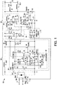
- Figs. 1 , 6 and 7 illustrate an exemplary LED driver or ballast circuit 100, which includes an AC input stage, a rectifier BR1, and an auto switching boost converter circuit 104 with a first switching device M1 that converts input power to a provide a DC bus.
- the circuit 100 also includes a buck DC-DC converter circuit 106 with a pulse width modulated switch M2 switching DC bus power via a transformer winding T1 and a diode D8 to drive an LED output load 108 in driver implementations ( Fig. 6 ).
- DC driver applications can include an inverter receiving the DC output of the boost converter 104 and driving an isolation transformer with an output rectifier for powering one or more LEDs.
- the illustrated circuit 100 can be used in ballast applications with the boost converter 104 (including the disclosed triac compatibility circuit 102) preceding an inverter 107 to drive AC powered light sources, such as fluorescent lamps 108.
- the driver 100 may be powered from a single-phase AC source 101 with dimming control via a phase-cut dimmer 200 coupled in series with the source 101 and the driver 100.
- the dimmer control 200 selectively cuts or interrupts current flow in portions of each cycle of the AC source 101 (phase cutting) using a triac T201 to dim the light output according to a user-adjustable resistance R201.
- the driver circuitry 100 is housed in a structure having an Edison base with AC input terminals.
- the driver 100 receives AC power from a single-phase input source and provides dimming functionality by operation of the phase-cut dimmer 200.
- a four-element rectifier bridge BR1 rectifies AC input power applied to the input terminals to provide a DC bus voltage across a capacitance C2, with a series inductance L1 and a diode D4 provided in an upper DC bus path following the capacitance C2, and an electrolytic capacitor C24 is coupled across the DC bus after the diode D4.
- a boost converter circuit 104 is thus provided, which includes a triac compatibility circuit 102 with an auto-switching (self-oscillating) driver circuit 103 operating the boost converter switch M1 to provide a boosted DC bus voltage across the electrolytic capacitor C4 using current provided by the inductor L1.
- the circuit 104 forms a continuous conduction boost converter that provides compatibility with triac-based dimmers by maintaining a constant current flowing through the input rectifier BR1 and any attached phase cut dimmer 200, independent of the instantaneous value of power line voltage.
- the minimum current level of the circuit 102 is determined by the minimum holding current of the triac of the phase-cut dimmer 200.
- the dimmer triacs typically have a holding current of 50ma or less.
- the illustrated circuit is designed to ensure at least 50ma flow to make sure that once the triac latches, it stays on and conducts for the rest of the power line half-cycle (until the next zero crossing). In this manner, the compatibility circuit 102 provides a load to the power line (whether interrupted by a phase-cutting triac or not) and embodiments can achieve high power factor, such as about 0.93 to 0.94.
- the regulated current level of the compatibility circuit 102 is set by the value of a sense resistor R8 of the self-oscillating circuit 103 to maintain a current flow slightly greater than the holding current of the external triac T201.
- a transorb D2 is connected across R8 for handling high bursts of energy, such as when line transients occur or during the initial power up where there may be an inrush of current to charge of the electrolytic capacitor C4.
- D2 is coupled across R8 to protect against large transients in the sensed current.
- a small input capacitor, C2 (15 nF in one embodiment) ensures that the triac T201 will latch without excessive ringing of the input current, and the self-oscillating circuit 103 of the boost converter thereafter maintains conduction of the triac.
- R8 is set so as to maintain at least 50mA triac holding current and input power as low as 6 Watts is possible.
- the illustrated circuit 106 thus facilitates flicker free light source operation when dimmed using wall dimmers, provides high power factor and complies with FCC Class B consumer requirements.
- the triac compatibility circuit 102 in Fig. 1 has an auto switching driver circuit 103 including a four layer switch configuration including PNP and NPN transistors Q1 and Q2, respectively, biased to an upper DC supply (VCC 15V provided by a power circuit 130 of the buck converter stage 106 in one example) via resistors R3 and R4, with a capacitor C1 stabilizing the supply VCC.
- the collector of Q1 is connected to the base of Q2 for SCR type operation and the base of Q1 operates as a trigger control terminal actuated by provision of sufficient base-emitter voltage via base resistor R7 according to the current flowing in the sense resistor R8.
- Q1 and Q2 turn on and off together, and the pair provides a signal through resistor R5 to a buffer formed by Q3 and Q4 (MBT3946DW in one implementation).
- the collector of the PNP transistor Q3 is connected to the supply line VCC by a resistor R9 and the collector of the NPN transistor Q4 is coupled to the ground terminal of M1 by a resistor R10.
- the pair Q3, Q4 operates as a buffer with the emitters connected to drive the gate of M1 high or low based on the trigger signal from Q1 and Q2 which is connected by resistor R5 to the bases of Q3 and Q4.
- the circuit 102 operates as an auto-switching or self-oscillating boost converter in conjunction with the switch M1, the inductor L1 and the diode D4, which self starts upon powerup.
- the circuit 102 moreover, optionally includes an overvoltage protection feature via a zener diode D3 and resistor R6, as well as an auto leveling circuit 120 formed by a capacitor C10, diode D9, and a resistor R11.
- the compatibility circuit 102 is auto-switching (self-oscillating) and thus the frequency is variable.
- the base circuit of Q1 senses the voltage across R8 via base resistor R7, and when the current through R8 is high enough, Q1 turns on to pull the base of Q2 low. This turns PNP transistor Q2 on, which operates the buffer formed by Q3 and Q4 to turn off the MOSFET switch M1 by Q3 turning off and Q4 turning on to pull the gate of M1 low.
- the reduced flow of current through M1 lowers the voltage across the sense resistor R8, thus turning Q1 and Q2 off. This allows the base of NPN transistor Q3 to rise thereby turning Q3 on and turning Q4 off.
- the triac compatibility circuit 102 thus provides a hysteretic auto-switching configuration that self-oscillates from power up and provides a continuous load to the power line during phase-cut dimming operation and otherwise.
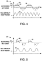
- the oscillation frequency 310 in Fig. 3 is a function of the inductance of L1 (e.g., 25mH in one embodiment) and the current sense resistor R8 (approximately 6 ⁇ in the example of Fig. 1 ).
- Fig. 3 illustrates a graph 300 showing the rectifier bridge input current 101 and the current 302 thereof which is conducted by the triac compatibility circuit 102, and graph 500 in Fig. 5 shows operation during phase-cut dimming.
- the compatibility circuit oscillation frequency 310 goes from zero at the power line zero crossings and increases to a point near the middle of the power line half-cycle where the electrolytic capacitor C4 charges through peak charging. This causes a current bump 304, after which the frequency 310 decreases back to zero at the next line power zero-crossing, and the process repeats.
- the hysteretic current 302 in the circuit 102 is a function of the boost converter configuration formed by the FET M1, the inductor L1 and the diode D4.
- the circuit 100 thus forms an auto-switching boost converter with the output capacitor C4 providing a DC bus for the subsequent converter stage 106, where the current is in the general form of a square wave 302 with small high frequency variations and the peak charging bumps 304 as shown in Fig. 3 , rather than following a sine wave.
- the auto leveling circuit 120 includes a capacitor C10, a diode D9, and a resistor R11 that connects to the base circuit of Q1.
- Resistor R11 has the same resistance value as the other base resistor R7 (510 ⁇ )
- D9 is an ordinary diode such as a 1N4148
- C10 is a 47uF capacitor in the illustrated embodiment.
- the circuit 120 performs temperature compensation and load regulation, for example to accommodate changes in the temperature of the base-emitter junction of Q1 and/or changing load conditions (e.g., load current increasing or decreasing). Such variations cause the voltage on the electrolytic capacitor C4 to change.
- the auto leveling circuit 120 compensates for these changes by essentially regulating the extent of the peak charging pulses (bumps 304) of the electrolytic bus capacitor C4. Circuit 120 measures the peak current flowing through the electrolytic capacitor C4 which supports the DC bus. If the current is too high, corresponding to a deficiency in the boost converter current, the driver circuit 103 will raise this current until the peak electrolytic current reduces to an acceptable level that maintains high power factor and low THD (e.g., less than about 35% in the illustrated embodiment). Conversely, if the peak current of C4 is too low, the circuit 120 will lower the current of the boost converter 104, thereby maintaining high power factor.
- THD e.g., less than about 35% in the illustrated embodiment
- the normal current 302 consumed by the compatibility circuit 102 is generally a square wave, with high frequency components along a nominal current level 306 and bumps or pulses 304 occurring during charging of C4.
- the switching frequency 310 of M1 by the self-oscillating circuit of Q1 and Q2 is zero at the start of the cycle, and is also zero at the bump 304. Between these points, the frequency 310 ramps up and then ramps down depending on the power line voltage.
- the maximum frequency points in Fig. 3 correspond to about 45 degrees, 135 degrees, 225 degrees, and 315 degrees.
- the bump 304 corresponds to the electrolytic capacitor C4 charging, because there is low FET switching frequency, so the capacitor C4 charges slightly.
- the triac compatibility circuit 102 also operates to provide steady current loading to meet the holding current requirements of a triac dimmer 200 during phase cutting.
- the compatibility circuit 102 also provides over-voltage protection. If the load increases, the nominal current level 306 will tend to decrease, but the duration and magnitude of the electrolytic capacitor peak-charging bump or spike 304 will increase. This is due to the sensed current through R8 (indicative of the load current) increasing, thereby forcing the FET M1 to stay off for longer at the charging occurrences 304. As the voltage across the sense resistor R8 increases, the capacitor C4 charges to a higher DC level. The increased voltage across R8 also causes an increase in the amount of charging of the auto-leveling circuit capacitor C10.
- a negative bias is applied to the base of Q1 by conduction of current from the auto-leveling capacitor C10 through resistor R11.
- This negative offset to the Q1 base voltage causes a delay in the turn-on of Q1 because the normal actuation via resistors R8 and R7 must counteract that bias to achieve the required base-emitter voltage to turn Q1 on.
- This delay allows the FET M1 to remain on for a longer time, thus raising the nominal current level to a higher value 308 seen in Fig. 4 , thereby counteracting the increased output load. Assuming the increased loading persists, the circuit will reach equilibrium at the higher nominal current level 308 at which the bump magnitude 304 is approximately what it was before the load change.
- the converse operation is provided for load decreases, with the circuit 120 reacting to reductions in the magnitude of the peak-charging bump 304 to provide offsetting positive bias to the Q1 base via capacitor C10 and resistor R11. Moreover, the circuit 120 counteracts thermal drift effects in the circuit components, such as changes to the base-emitter junctions of the transistor Q1, etc. Thus, the auto-leveling circuit 120 provides stability in regulating against load fluctuations, temperature variations, etc.
- the circuit 102 also includes over-voltage protection components D3 and R6. When the output of the system 100 is unloaded, this circuitry prevents the DC bus from climbing beyond the design target.
- this transient voltage suppressor TVS senses the DC bus of the boost converter by connection of the zener diode D3 to the positive terminal of the bus capacitor C4.
- the zener D3 is connected in series with a resistor R6 that is connected to the base of Q1. If the output load is removed or its impedance increases significantly, the closed loop operation of the boost converter will cause the voltage of the electrolytic capacitor C4 to increase.
- the over-voltage protection zener diode D3 (e.g., SMF170A with a 170 volt Vz in one example) starts to conduct.
- current is provided through the resistor R6 to the base of Q1, which turns on Q1 and Q2, and the buffer formed by Q3 and Q4 will turn off the FET M1, essentially providing a positive bias to the Q1 base circuit to cause the M1 shutoff to occur sooner.
- the voltage across C4 continues to rise, a point can be reached where the operation of the Q1 base circuit biasing via zener D3 and resistor R6 will cause M1 to significantly reduce the current flow by going to a high frequency operating state.
- the circuit will stabilize with the voltage across C4 slightly above the rectified line voltage level with M1 being switched at a high frequency to effectively limit the amount of current flowing through M1.
- the triac compatibility circuit 102 provides auto-switching functionality in combination with over-voltage protection.
- the circuit 100 can be used as a DC driver for an LED array type light source load 108, or can be used as an initial stage followed by an inverter 107 for powering a fluorescent lamp light source 108 in a ballast configuration.
- a pulse width modulated buck type power circuit 106 receives the DC bus voltage across C4 and includes a second power switch (e.g., MOSFET) M2.
- M2 operates according to a pulse width modulated control input signal applied by a PWM controller or driver U1 to the gate of M2 to control application of DC power to an output load 108, such as an LED array or a subsequent inverter stage 107.
- the controller U1 in certain embodiments can be a transition mode power factor correction (PFC) controller L6562 IC available from Intersil and STMicroelectronics.
- U1 has an amplifier input INV coupled with an internal error amplifier, as well as a gain input MULT and an internal pulse width modulator with a drive output GD providing the PWM control signal to the gate of M2 to set the output power level based at least in part on the amplifier input INV and the gain input MULT.
- PFC transition mode power factor correction
- the switch M2 is thus connected in series between the winding TIC and the circuit ground GND along with a series-connected sense resistor R19. As primary current flows through the series circuit, the current through R19 provides a corresponding voltage at a comparator input terminal CS of the controller U1 for cycle-to-cycle control of the primary current.
- the drive output GD provides a pulse width modulated control signal via resistor R18 to the gate of M2 at least partially according to the sensed load current, the amplifier input INV, and the gain input MULT.
- U1 includes an on-board error amplifier with an inverting input INV and an output COMP to allow external connection of a compensation network between the INV and COMP pins.
- resistor R16 and capacitor C6 are connected as shown in Fig.
- the illustrated embodiment uses the multiplier input MULT as a dimming control input to change the duty cycle of the gate drive signal GS and thus the level of the output current.
- the input to the input MULT is a DC voltage proportional to the rectified average of the power line voltage. A triac will reduce this voltage as it reduces the angle during which current can flow.
- the current flowing in M2 is sensed via the resistor R19, and the resulting voltage V S is applied to the CS pin and compared with a reference generated by the multiplier to determine the MOSFET's turn-off.
- the gate drive output GD is selectively disabled according to the ZCD input signal status for transition-mode operation, where a negative-going edge triggers the MOSFET's turn-on. This advantageously allows connection to an optional zero current detection circuit 140 such that the switch M2 will turn on when the current through the primary winding T1C is zero.
- the ground pin GND provides a current return path for both the signal part and the gate driver circuitry of U1.
- a zero crossing detection circuit 140 which includes sense windings T1A and T1B wound on the core of transformer T1 and magnetically coupled with the primary winding TIC.
- Circuit 140 also includes a center node connecting T1A and TIB with capacitor C8. The lower terminal of C8 is coupled to VCC through diode D6 and to ground through diode D7, and a bypass capacitor C7 is connected from VCC to ground GND.
- the zero crossing circuit 140 senses a zero crossing condition of the primary winding TIC using the sense windings T1A and TIB and selectively provides a signal to the zero crossing detect input ZCD of the PWM controller U1 via resistor R14 indicating a sensed zero crossing condition of the primary winding TIC.
- the illustrated circuit also includes a power circuit 130 providing the control voltage VCC (e.g., 15 volts in one embodiment) for use by both the controller U1 and the triac compatibility circuit 102.
- the power circuit 130 includes a PNP transistor Q5 with a collector coupled to the upper DC bus line via resistor R13 and a gate coupled to the upper DC bus by resistor R12 and to the circuit ground GND via a 14V zener diode D5.
- a sensing circuit 110 ( Fig. 1 ) is coupled with the input terminals to provide a sensor signal to the gain input MULT of U1.
- the sensing circuit 110 in the illustrated embodiment generates the sensor signal via a resistor R1 coupled between a first AC input terminal and the gain input MULT and a second resistor R2 coupled between the second AC input terminal and the gain input MULT, with the resistors R1 and R2 forming a voltage divider with a resistor R15 coupled from the MULT terminal to ground GND, and a filter capacitor C5 connected in parallel across R15.
- the sensing circuit 110 provides the sensor signal to the gain input MULT as a full-wave rectified waveform with a DC level corresponding to the applied input voltage.
- the MULT input signal value will be reduced when a phase-cutting dimmer 200 is operated for dimming the light source output.
- the controller U1 modifies the pulse width modulated output at the GD terminal according to the MULT input signal value to selectively reduce the DC output power provided to the load.
Landscapes
- Circuit Arrangement For Electric Light Sources In General (AREA)
- Rectifiers (AREA)
- Dc-Dc Converters (AREA)
Claims (9)
- Circuit (100) pour alimenter en énergie au moins une source de lumière, comprenant :un redresseur ayant des bornes d'entrée en courant alternatif CA pour recevoir une énergie d'entrée CA et des première et seconde bornes de sortie en courant continu CC pour fournir de l'énergie redressée CC ;un convertisseur d'amplification recevant l'énergie CC redressée en provenance du redresseur et fournissant une première sortie CC, le convertisseur d'amplification comprenant :une inductance ayant une première borne couplée à la première borne de sortie CC du redresseur et une seconde borne,une diode avec une anode couplée à la seconde borne de l'inductance et une cathode,une capacité de bus avec une première borne couplée à la cathode de la diode et une seconde borne couplée à un noeud de masse de circuit, etun circuit de compatibilité de triac (102), comprenant :un dispositif de commutation couplé entre l'anode de la diode et la masse de circuit et incluant une borne de commande, le dispositif de commutation étant opérationnel pour coupler de manière sélective électriquement l'anode de la diode et la masse de circuit ou pour déconnecter l'anode de la diode depuis la masse de circuit selon un signal reçu au niveau de la borne de commande, etun circuit de pilotage de commutation auto (103) incluant une résistance de détection (R8) couplée entre la masse de circuit et la seconde borne de sortie CC du redresseur pour détecter un courant s'écoulant dans le dispositif de commutation, le circuit de pilotage de commutation auto étant opérationnel pour fournir un signal de commande de commutation alternatif de fréquence variable à la borne de commande du dispositif de commutation sur la base au moins en partie d'une tension aux bornes de la résistance de détection pour fournir un flux de courant régulé dans le convertisseur d'amplification indépendant d'une coupure de phase au niveau des bornes d'entrée CA du redresseur ; caractérisé en ce que :un circuit convertisseur CC-CC (106) avec des bornes d'entrée CC couplées aux première et seconde bornes de la capacité de bus, et des bornes de sortie CC fournissant une seconde sortie CC pour fournir directement ou indirectement de l'énergie à au moins une source de lumière,où le circuit de compatibilité de triac (102) comprend un circuit de mise à niveau auto couplé de manière opérationnelle au circuit de pilotage de commutation auto (103) pour ajuster de manière sélective le flux de courant dans le convertisseur d'amplification sur la base d'au moins un de changements de température dans le circuit et de changements de charge dans le circuit ; etoù le circuit de mise à niveau auto comprend :un condensateur avec une première borne connectée à la masse de circuit et une seconde borne ;une diode avec une anode connectée à la seconde borne du condensateur et une cathode connectée à la seconde borne de sortie CC du redresseur ; etune résistance couplée entre l'anode de la diode et une borne de commande de commutateur du circuit de pilotage de commutation auto pour fournir un signal provenant du condensateur pour ajuster de manière sélective le flux de courant dans le convertisseur d'amplification.
- Circuit (100) selon la revendication 1, où le circuit convertisseur CC-CC (106) est un convertisseur abaisseur de tension fournissant une sortie pour piloter au moins une source de lumière LED.
- Circuit (100) selon la revendication 1, comprenant un onduleur recevant la seconde sortie CC en provenance du circuit convertisseur CC-CC (106) et fournissant une sortie CA pour alimenter en énergie au moins une lampe fluorescente.
- Circuit (100) selon la revendication 1, où le circuit de compatibilité de triac (102) comprend un circuit de protection contre les surtensions couplé de manière opérationnelle au circuit de pilotage de commutation auto (103) pour ajuster de manière sélective le flux de courant dans le convertisseur d'amplification pour limiter une tension aux bornes de la capacité de bus.
- Circuit (100) selon la revendication 4, où le circuit de protection contre les surtensions comprend :une diode Zener avec une cathode couplée à la première borne de la capacité de bus et une anode ; etune résistance couplée entre l'anode de la diode Zener et la borne de commande de commutateur du circuit de pilotage de commutation auto (103) pour fournir un signal en provenance de la diode Zener pour ajuster de manière sélective le flux de courant dans le convertisseur d'amplification sur la base au moins partiellement de la tension aux bornes de la capacité de bus.
- Circuit (100) selon la revendication 1, où le circuit de compatibilité de triac (102) comprend un circuit de protection contre les surtensions couplé de manière opérationnelle au circuit de pilotage de commutation auto pour ajuster de manière sélective le flux de courant dans le convertisseur d'amplification pour limiter une tension aux bornes de la capacité de bus.
- Circuit (100) selon la revendication 6, où le circuit de protection contre les surtensions comprend :une diode Zener avec une cathode couplée à la première borne de la capacité de bus et une anode ; etune résistance couplée entre l'anode de la diode Zener et une borne de commande de commutateur du circuit de pilotage de commutation auto (103) pour fournir un signal en provenance de la diode Zener pour ajuster de manière sélective le flux de courant dans le convertisseur d'amplification sur la base au moins partiellement de la tension aux bornes de la capacité de bus.
- Circuit (100) selon la revendication 1, où le circuit de compatibilité de triac (102) comprend un circuit de protection contre les surtensions couplé de manière opérationnelle au circuit de pilotage de commutation auto (103) pour ajuster de manière sélective le flux de courant dans le convertisseur d'amplification pour limiter une tension aux bornes de la capacité de bus.
- Circuit (100) selon la revendication 8, où le circuit de protection contre les surtensions comprend :une diode Zener avec une cathode couplée à la première borne de la capacité de bus et une anode ; etune résistance couplée entre l'anode de la diode Zener et une borne de commande de commutateur du circuit de pilotage de commutation auto (103) pour fournir un signal en provenance de la diode Zener pour ajuster de manière sélective le flux de courant dans le convertisseur d'amplification sur la base au moins partiellement de la tension aux bornes de la capacité de bus.
Applications Claiming Priority (2)
| Application Number | Priority Date | Filing Date | Title |
|---|---|---|---|
| US13/045,921 US8497636B2 (en) | 2011-03-11 | 2011-03-11 | Auto-switching triac compatibility circuit with auto-leveling and overvoltage protection |
| PCT/US2012/025839 WO2012125260A1 (fr) | 2011-03-11 | 2012-02-21 | Circuit de compatibilité triac à auto-commutation avec auto-nivellement et protection contre les surtensions |
Publications (2)
| Publication Number | Publication Date |
|---|---|
| EP2684423A1 EP2684423A1 (fr) | 2014-01-15 |
| EP2684423B1 true EP2684423B1 (fr) | 2018-11-28 |
Family
ID=45929594
Family Applications (1)
| Application Number | Title | Priority Date | Filing Date |
|---|---|---|---|
| EP12712162.2A Not-in-force EP2684423B1 (fr) | 2011-03-11 | 2012-02-21 | Circuit de compatibilité triac à auto-commutation avec auto-nivellement et protection contre les surtensions |
Country Status (5)
| Country | Link |
|---|---|
| US (1) | US8497636B2 (fr) |
| EP (1) | EP2684423B1 (fr) |
| CN (1) | CN103430623B (fr) |
| MX (1) | MX2013010432A (fr) |
| WO (1) | WO2012125260A1 (fr) |
Families Citing this family (21)
| Publication number | Priority date | Publication date | Assignee | Title |
|---|---|---|---|---|
| US8866403B2 (en) * | 2010-12-09 | 2014-10-21 | General Electric Company | 3-way, phase-cut dimmable LED driver |
| US9060397B2 (en) * | 2011-07-15 | 2015-06-16 | General Electric Company | High voltage LED and driver |
| US8704451B2 (en) * | 2011-10-07 | 2014-04-22 | Excelliance Mos Corporation | Driving circuit of light emitting diode |
| JP2013118132A (ja) * | 2011-12-05 | 2013-06-13 | Panasonic Corp | 点灯装置およびそれを備えた照明器具 |
| GB2507308A (en) * | 2012-10-25 | 2014-04-30 | Spled Ltd | LED module driver |
| EP2958404B1 (fr) * | 2013-02-13 | 2017-09-06 | Shindengen Electric Manufacturing Co., Ltd. | Circuit de commande de gradation d'intensité lumineuse d'éclairage à diodes électroluminescentes et procédé de gradation d'intensité lumineuse d'éclairage à diodes électroluminescentes |
| US9204505B2 (en) * | 2013-04-29 | 2015-12-01 | Stmicroelectronics, Inc. | Power converter for interfacing a fluorescent lighting ballast to a light emitting diode lamp |
| WO2014188228A1 (fr) * | 2013-05-22 | 2014-11-27 | Lau Chun To | Réamorçage de mise sous tension pour gradateur à led |
| US9368073B2 (en) * | 2013-08-12 | 2016-06-14 | Shenzhen China Star Optoelectronics Technology Co., Ltd. | LED backlight driving circuit and LCD |
| US9661711B2 (en) * | 2013-08-19 | 2017-05-23 | Infineon Technologies Austria Ag | Multi-function pin for light emitting diode (LED) driver |
| US9332602B2 (en) * | 2013-12-12 | 2016-05-03 | Genereal Electric Company | LED driver with transformerless hysteretic boost |
| US9468054B2 (en) | 2014-06-10 | 2016-10-11 | Lunera Lighting, Inc. | Retrofit LED lighting system with circuit level enhancement |
| US9237621B1 (en) * | 2014-08-22 | 2016-01-12 | Universal Lighting Technologies, Inc. | Current control circuit and method for floating IC driven buck-boost converter |
| US9927821B2 (en) | 2016-05-25 | 2018-03-27 | Innovative Building Energy Control | Building energy control systems and methods |
| US10806008B2 (en) * | 2016-05-25 | 2020-10-13 | Innovative Building Energy Control | Building energy control systems and methods |
| US10360485B2 (en) * | 2016-08-29 | 2019-07-23 | Integrated Device Technology, Inc. | Circuits and systems for low power magnetic secure transmission |
| JP6800723B2 (ja) * | 2016-12-05 | 2020-12-16 | 株式会社ミツトヨ | エンコーダ及びエンコーダの光源 |
| US11387743B2 (en) * | 2017-07-20 | 2022-07-12 | Panasonic Intellectual Property Management Co., Ltd. | Power supply device and control method for stably operating a device when a frequency of an input power supply fluctuates |
| CN107658843B (zh) * | 2017-10-23 | 2023-11-14 | 美智光电科技股份有限公司 | 过压保护电路和灯具 |
| CA3089368C (fr) * | 2018-01-23 | 2021-06-15 | DMF, Inc. | Procedes et appareil de gradation de del a base de triac |
| WO2022056180A1 (fr) | 2020-09-09 | 2022-03-17 | DMF, Inc. | Appareil et procédés de communication d'informations et de puissance par l'intermédiaire de formes d'onde ca à coupure de phase |
Citations (4)
| Publication number | Priority date | Publication date | Assignee | Title |
|---|---|---|---|---|
| US6150771A (en) * | 1997-06-11 | 2000-11-21 | Precision Solar Controls Inc. | Circuit for interfacing between a conventional traffic signal conflict monitor and light emitting diodes replacing a conventional incandescent bulb in the signal |
| US6181075B1 (en) * | 1989-10-16 | 2001-01-30 | Everbrite Electronics, Inc. | Power supply circuit for gas discharge tube |
| WO2009011898A2 (fr) * | 2007-07-17 | 2009-01-22 | I/O Controls Corporation | Réseau de commande pour système d'éclairage à base de diodes électroluminescentes dans un véhicule de transport en commun |
| WO2010146529A1 (fr) * | 2009-06-18 | 2010-12-23 | Koninklijke Philips Electronics N.V. | Interface d'alimentation à del pour gradateur à triac |
Family Cites Families (6)
| Publication number | Priority date | Publication date | Assignee | Title |
|---|---|---|---|---|
| US5430356A (en) * | 1993-10-05 | 1995-07-04 | Lutron Electronics Co., Inc. | Programmable lighting control system with normalized dimming for different light sources |
| US6373200B1 (en) | 2000-07-31 | 2002-04-16 | General Electric Company | Interface circuit and method |
| US8547035B2 (en) * | 2009-07-15 | 2013-10-01 | Crestron Electronics Inc. | Dimmer adaptable to either two or three active wires |
| US8294379B2 (en) * | 2009-11-10 | 2012-10-23 | Green Mark Technology Inc. | Dimmable LED lamp and dimmable LED lighting apparatus |
| US8111017B2 (en) * | 2010-07-12 | 2012-02-07 | O2Micro, Inc | Circuits and methods for controlling dimming of a light source |
| US8446099B2 (en) * | 2010-10-04 | 2013-05-21 | Earl W. McCune, Jr. | Power conversion and control systems and methods for solid-state lighting |
-
2011
- 2011-03-11 US US13/045,921 patent/US8497636B2/en active Active
-
2012
- 2012-02-21 EP EP12712162.2A patent/EP2684423B1/fr not_active Not-in-force
- 2012-02-21 WO PCT/US2012/025839 patent/WO2012125260A1/fr active Application Filing
- 2012-02-21 CN CN201280012770.7A patent/CN103430623B/zh active Active
- 2012-02-21 MX MX2013010432A patent/MX2013010432A/es active IP Right Grant
Patent Citations (4)
| Publication number | Priority date | Publication date | Assignee | Title |
|---|---|---|---|---|
| US6181075B1 (en) * | 1989-10-16 | 2001-01-30 | Everbrite Electronics, Inc. | Power supply circuit for gas discharge tube |
| US6150771A (en) * | 1997-06-11 | 2000-11-21 | Precision Solar Controls Inc. | Circuit for interfacing between a conventional traffic signal conflict monitor and light emitting diodes replacing a conventional incandescent bulb in the signal |
| WO2009011898A2 (fr) * | 2007-07-17 | 2009-01-22 | I/O Controls Corporation | Réseau de commande pour système d'éclairage à base de diodes électroluminescentes dans un véhicule de transport en commun |
| WO2010146529A1 (fr) * | 2009-06-18 | 2010-12-23 | Koninklijke Philips Electronics N.V. | Interface d'alimentation à del pour gradateur à triac |
Also Published As
| Publication number | Publication date |
|---|---|
| US20120229044A1 (en) | 2012-09-13 |
| MX2013010432A (es) | 2013-10-03 |
| WO2012125260A1 (fr) | 2012-09-20 |
| CN103430623B (zh) | 2016-08-24 |
| US8497636B2 (en) | 2013-07-30 |
| EP2684423A1 (fr) | 2014-01-15 |
| CN103430623A (zh) | 2013-12-04 |
Similar Documents
| Publication | Publication Date | Title |
|---|---|---|
| EP2684423B1 (fr) | Circuit de compatibilité triac à auto-commutation avec auto-nivellement et protection contre les surtensions | |
| US9148922B2 (en) | Power conversion apparatus and system for solid state lighting | |
| US8704462B2 (en) | Adaptive current regulation for solid state lighting | |
| US8558470B2 (en) | Adaptive current regulation for solid state lighting | |
| US8698407B1 (en) | Highly integrated non-inductive LED driver | |
| EP2567596B1 (fr) | Unité d'alimentation de del pourvue d'une commande de gradation à triac | |
| US10149362B2 (en) | Solid state lighting control with dimmer interface to control brightness | |
| US8847515B2 (en) | Multi-mode dimmer interfacing including attach state control | |
| JP6103478B2 (ja) | 電源回路及び照明装置 | |
| CN107071955B (zh) | 用于固态光源的可调光多通道驱动器 | |
| US8575850B2 (en) | System and method for supplying constant power to luminuous loads with power factor correction | |
| JP6617136B2 (ja) | Ledドライバ回路、led回路、及び駆動方法 | |
| US8575853B2 (en) | System and method for supplying constant power to luminuous loads | |
| JP2015503193A (ja) | 高電圧ledコンポーネントを含む固体照明装置のための駆動回路及び関連方法 | |
| EP3155715B1 (fr) | Circuits d'alimentation électrique | |
| US20140285099A1 (en) | Power Supply Circuit and Illumination Apparatus | |
| US11452189B2 (en) | External zero-crossing detection circuit for LED drivers | |
| KR102207025B1 (ko) | 디밍 led 회로 증강 dc/dc 제어기 집적 회로 | |
| JP2020194744A (ja) | 照明装置 |
Legal Events
| Date | Code | Title | Description |
|---|---|---|---|
| PUAI | Public reference made under article 153(3) epc to a published international application that has entered the european phase |
Free format text: ORIGINAL CODE: 0009012 |
|
| 17P | Request for examination filed |
Effective date: 20131011 |
|
| AK | Designated contracting states |
Kind code of ref document: A1 Designated state(s): AL AT BE BG CH CY CZ DE DK EE ES FI FR GB GR HR HU IE IS IT LI LT LU LV MC MK MT NL NO PL PT RO RS SE SI SK SM TR |
|
| DAX | Request for extension of the european patent (deleted) | ||
| STAA | Information on the status of an ep patent application or granted ep patent |
Free format text: STATUS: EXAMINATION IS IN PROGRESS |
|
| 17Q | First examination report despatched |
Effective date: 20170228 |
|
| GRAP | Despatch of communication of intention to grant a patent |
Free format text: ORIGINAL CODE: EPIDOSNIGR1 |
|
| STAA | Information on the status of an ep patent application or granted ep patent |
Free format text: STATUS: GRANT OF PATENT IS INTENDED |
|
| INTG | Intention to grant announced |
Effective date: 20180730 |
|
| GRAS | Grant fee paid |
Free format text: ORIGINAL CODE: EPIDOSNIGR3 |
|
| GRAA | (expected) grant |
Free format text: ORIGINAL CODE: 0009210 |
|
| STAA | Information on the status of an ep patent application or granted ep patent |
Free format text: STATUS: THE PATENT HAS BEEN GRANTED |
|
| AK | Designated contracting states |
Kind code of ref document: B1 Designated state(s): AL AT BE BG CH CY CZ DE DK EE ES FI FR GB GR HR HU IE IS IT LI LT LU LV MC MK MT NL NO PL PT RO RS SE SI SK SM TR |
|
| REG | Reference to a national code |
Ref country code: GB Ref legal event code: FG4D |
|
| REG | Reference to a national code |
Ref country code: CH Ref legal event code: EP |
|
| REG | Reference to a national code |
Ref country code: AT Ref legal event code: REF Ref document number: 1071827 Country of ref document: AT Kind code of ref document: T Effective date: 20181215 |
|
| REG | Reference to a national code |
Ref country code: DE Ref legal event code: R096 Ref document number: 602012054033 Country of ref document: DE |
|
| REG | Reference to a national code |
Ref country code: IE Ref legal event code: FG4D |
|
| REG | Reference to a national code |
Ref country code: NL Ref legal event code: MP Effective date: 20181128 |
|
| REG | Reference to a national code |
Ref country code: LT Ref legal event code: MG4D |
|
| REG | Reference to a national code |
Ref country code: AT Ref legal event code: MK05 Ref document number: 1071827 Country of ref document: AT Kind code of ref document: T Effective date: 20181128 |
|
| PG25 | Lapsed in a contracting state [announced via postgrant information from national office to epo] |
Ref country code: BG Free format text: LAPSE BECAUSE OF FAILURE TO SUBMIT A TRANSLATION OF THE DESCRIPTION OR TO PAY THE FEE WITHIN THE PRESCRIBED TIME-LIMIT Effective date: 20190228 Ref country code: FI Free format text: LAPSE BECAUSE OF FAILURE TO SUBMIT A TRANSLATION OF THE DESCRIPTION OR TO PAY THE FEE WITHIN THE PRESCRIBED TIME-LIMIT Effective date: 20181128 Ref country code: LV Free format text: LAPSE BECAUSE OF FAILURE TO SUBMIT A TRANSLATION OF THE DESCRIPTION OR TO PAY THE FEE WITHIN THE PRESCRIBED TIME-LIMIT Effective date: 20181128 Ref country code: HR Free format text: LAPSE BECAUSE OF FAILURE TO SUBMIT A TRANSLATION OF THE DESCRIPTION OR TO PAY THE FEE WITHIN THE PRESCRIBED TIME-LIMIT Effective date: 20181128 Ref country code: AT Free format text: LAPSE BECAUSE OF FAILURE TO SUBMIT A TRANSLATION OF THE DESCRIPTION OR TO PAY THE FEE WITHIN THE PRESCRIBED TIME-LIMIT Effective date: 20181128 Ref country code: LT Free format text: LAPSE BECAUSE OF FAILURE TO SUBMIT A TRANSLATION OF THE DESCRIPTION OR TO PAY THE FEE WITHIN THE PRESCRIBED TIME-LIMIT Effective date: 20181128 Ref country code: ES Free format text: LAPSE BECAUSE OF FAILURE TO SUBMIT A TRANSLATION OF THE DESCRIPTION OR TO PAY THE FEE WITHIN THE PRESCRIBED TIME-LIMIT Effective date: 20181128 Ref country code: IS Free format text: LAPSE BECAUSE OF FAILURE TO SUBMIT A TRANSLATION OF THE DESCRIPTION OR TO PAY THE FEE WITHIN THE PRESCRIBED TIME-LIMIT Effective date: 20190328 Ref country code: NO Free format text: LAPSE BECAUSE OF FAILURE TO SUBMIT A TRANSLATION OF THE DESCRIPTION OR TO PAY THE FEE WITHIN THE PRESCRIBED TIME-LIMIT Effective date: 20190228 |
|
| PG25 | Lapsed in a contracting state [announced via postgrant information from national office to epo] |
Ref country code: AL Free format text: LAPSE BECAUSE OF FAILURE TO SUBMIT A TRANSLATION OF THE DESCRIPTION OR TO PAY THE FEE WITHIN THE PRESCRIBED TIME-LIMIT Effective date: 20181128 Ref country code: GR Free format text: LAPSE BECAUSE OF FAILURE TO SUBMIT A TRANSLATION OF THE DESCRIPTION OR TO PAY THE FEE WITHIN THE PRESCRIBED TIME-LIMIT Effective date: 20190301 Ref country code: PT Free format text: LAPSE BECAUSE OF FAILURE TO SUBMIT A TRANSLATION OF THE DESCRIPTION OR TO PAY THE FEE WITHIN THE PRESCRIBED TIME-LIMIT Effective date: 20190328 Ref country code: RS Free format text: LAPSE BECAUSE OF FAILURE TO SUBMIT A TRANSLATION OF THE DESCRIPTION OR TO PAY THE FEE WITHIN THE PRESCRIBED TIME-LIMIT Effective date: 20181128 Ref country code: SE Free format text: LAPSE BECAUSE OF FAILURE TO SUBMIT A TRANSLATION OF THE DESCRIPTION OR TO PAY THE FEE WITHIN THE PRESCRIBED TIME-LIMIT Effective date: 20181128 |
|
| PG25 | Lapsed in a contracting state [announced via postgrant information from national office to epo] |
Ref country code: NL Free format text: LAPSE BECAUSE OF FAILURE TO SUBMIT A TRANSLATION OF THE DESCRIPTION OR TO PAY THE FEE WITHIN THE PRESCRIBED TIME-LIMIT Effective date: 20181128 |
|
| PG25 | Lapsed in a contracting state [announced via postgrant information from national office to epo] |
Ref country code: CZ Free format text: LAPSE BECAUSE OF FAILURE TO SUBMIT A TRANSLATION OF THE DESCRIPTION OR TO PAY THE FEE WITHIN THE PRESCRIBED TIME-LIMIT Effective date: 20181128 Ref country code: IT Free format text: LAPSE BECAUSE OF FAILURE TO SUBMIT A TRANSLATION OF THE DESCRIPTION OR TO PAY THE FEE WITHIN THE PRESCRIBED TIME-LIMIT Effective date: 20181128 Ref country code: PL Free format text: LAPSE BECAUSE OF FAILURE TO SUBMIT A TRANSLATION OF THE DESCRIPTION OR TO PAY THE FEE WITHIN THE PRESCRIBED TIME-LIMIT Effective date: 20181128 Ref country code: DK Free format text: LAPSE BECAUSE OF FAILURE TO SUBMIT A TRANSLATION OF THE DESCRIPTION OR TO PAY THE FEE WITHIN THE PRESCRIBED TIME-LIMIT Effective date: 20181128 |
|
| REG | Reference to a national code |
Ref country code: DE Ref legal event code: R097 Ref document number: 602012054033 Country of ref document: DE |
|
| PG25 | Lapsed in a contracting state [announced via postgrant information from national office to epo] |
Ref country code: EE Free format text: LAPSE BECAUSE OF FAILURE TO SUBMIT A TRANSLATION OF THE DESCRIPTION OR TO PAY THE FEE WITHIN THE PRESCRIBED TIME-LIMIT Effective date: 20181128 Ref country code: SM Free format text: LAPSE BECAUSE OF FAILURE TO SUBMIT A TRANSLATION OF THE DESCRIPTION OR TO PAY THE FEE WITHIN THE PRESCRIBED TIME-LIMIT Effective date: 20181128 Ref country code: SK Free format text: LAPSE BECAUSE OF FAILURE TO SUBMIT A TRANSLATION OF THE DESCRIPTION OR TO PAY THE FEE WITHIN THE PRESCRIBED TIME-LIMIT Effective date: 20181128 Ref country code: RO Free format text: LAPSE BECAUSE OF FAILURE TO SUBMIT A TRANSLATION OF THE DESCRIPTION OR TO PAY THE FEE WITHIN THE PRESCRIBED TIME-LIMIT Effective date: 20181128 |
|
| REG | Reference to a national code |
Ref country code: DE Ref legal event code: R119 Ref document number: 602012054033 Country of ref document: DE |
|
| REG | Reference to a national code |
Ref country code: CH Ref legal event code: PL |
|
| PLBE | No opposition filed within time limit |
Free format text: ORIGINAL CODE: 0009261 |
|
| STAA | Information on the status of an ep patent application or granted ep patent |
Free format text: STATUS: NO OPPOSITION FILED WITHIN TIME LIMIT |
|
| GBPC | Gb: european patent ceased through non-payment of renewal fee |
Effective date: 20190228 |
|
| PG25 | Lapsed in a contracting state [announced via postgrant information from national office to epo] |
Ref country code: LU Free format text: LAPSE BECAUSE OF NON-PAYMENT OF DUE FEES Effective date: 20190221 Ref country code: SI Free format text: LAPSE BECAUSE OF FAILURE TO SUBMIT A TRANSLATION OF THE DESCRIPTION OR TO PAY THE FEE WITHIN THE PRESCRIBED TIME-LIMIT Effective date: 20181128 Ref country code: MC Free format text: LAPSE BECAUSE OF FAILURE TO SUBMIT A TRANSLATION OF THE DESCRIPTION OR TO PAY THE FEE WITHIN THE PRESCRIBED TIME-LIMIT Effective date: 20181128 |
|
| 26N | No opposition filed |
Effective date: 20190829 |
|
| REG | Reference to a national code |
Ref country code: BE Ref legal event code: MM Effective date: 20190228 |
|
| REG | Reference to a national code |
Ref country code: IE Ref legal event code: MM4A |
|
| PG25 | Lapsed in a contracting state [announced via postgrant information from national office to epo] |
Ref country code: CH Free format text: LAPSE BECAUSE OF NON-PAYMENT OF DUE FEES Effective date: 20190228 Ref country code: LI Free format text: LAPSE BECAUSE OF NON-PAYMENT OF DUE FEES Effective date: 20190228 |
|
| PG25 | Lapsed in a contracting state [announced via postgrant information from national office to epo] |
Ref country code: DE Free format text: LAPSE BECAUSE OF NON-PAYMENT OF DUE FEES Effective date: 20190903 Ref country code: IE Free format text: LAPSE BECAUSE OF NON-PAYMENT OF DUE FEES Effective date: 20190221 Ref country code: GB Free format text: LAPSE BECAUSE OF NON-PAYMENT OF DUE FEES Effective date: 20190228 |
|
| PG25 | Lapsed in a contracting state [announced via postgrant information from national office to epo] |
Ref country code: FR Free format text: LAPSE BECAUSE OF NON-PAYMENT OF DUE FEES Effective date: 20190228 Ref country code: BE Free format text: LAPSE BECAUSE OF NON-PAYMENT OF DUE FEES Effective date: 20190228 |
|
| PG25 | Lapsed in a contracting state [announced via postgrant information from national office to epo] |
Ref country code: TR Free format text: LAPSE BECAUSE OF FAILURE TO SUBMIT A TRANSLATION OF THE DESCRIPTION OR TO PAY THE FEE WITHIN THE PRESCRIBED TIME-LIMIT Effective date: 20181128 |
|
| PG25 | Lapsed in a contracting state [announced via postgrant information from national office to epo] |
Ref country code: MT Free format text: LAPSE BECAUSE OF NON-PAYMENT OF DUE FEES Effective date: 20190221 |
|
| PG25 | Lapsed in a contracting state [announced via postgrant information from national office to epo] |
Ref country code: CY Free format text: LAPSE BECAUSE OF FAILURE TO SUBMIT A TRANSLATION OF THE DESCRIPTION OR TO PAY THE FEE WITHIN THE PRESCRIBED TIME-LIMIT Effective date: 20181128 |
|
| PG25 | Lapsed in a contracting state [announced via postgrant information from national office to epo] |
Ref country code: HU Free format text: LAPSE BECAUSE OF FAILURE TO SUBMIT A TRANSLATION OF THE DESCRIPTION OR TO PAY THE FEE WITHIN THE PRESCRIBED TIME-LIMIT; INVALID AB INITIO Effective date: 20120221 |
|
| PG25 | Lapsed in a contracting state [announced via postgrant information from national office to epo] |
Ref country code: MK Free format text: LAPSE BECAUSE OF FAILURE TO SUBMIT A TRANSLATION OF THE DESCRIPTION OR TO PAY THE FEE WITHIN THE PRESCRIBED TIME-LIMIT Effective date: 20181128 |