EP2681780B1 - Method of tuning work function of metal nanostructure-based transparent conductor - Google Patents
Method of tuning work function of metal nanostructure-based transparent conductor Download PDFInfo
- Publication number
- EP2681780B1 EP2681780B1 EP12710827.2A EP12710827A EP2681780B1 EP 2681780 B1 EP2681780 B1 EP 2681780B1 EP 12710827 A EP12710827 A EP 12710827A EP 2681780 B1 EP2681780 B1 EP 2681780B1
- Authority
- EP
- European Patent Office
- Prior art keywords
- dipole
- metal
- metal nanostructure
- work function
- nanostructures
- Prior art date
- Legal status (The legal status is an assumption and is not a legal conclusion. Google has not performed a legal analysis and makes no representation as to the accuracy of the status listed.)
- Not-in-force
Links
- 239000002086 nanomaterial Substances 0.000 title claims description 95
- 229910052751 metal Inorganic materials 0.000 title claims description 81
- 239000002184 metal Substances 0.000 title claims description 81
- 238000000034 method Methods 0.000 title claims description 24
- 239000004020 conductor Substances 0.000 title description 10
- 239000003446 ligand Substances 0.000 claims description 56
- 239000000203 mixture Substances 0.000 claims description 24
- 239000000758 substrate Substances 0.000 claims description 24
- 239000002344 surface layer Substances 0.000 claims description 24
- 239000004094 surface-active agent Substances 0.000 claims description 23
- 238000000576 coating method Methods 0.000 claims description 16
- 239000011248 coating agent Substances 0.000 claims description 15
- 230000001965 increasing effect Effects 0.000 claims description 9
- 125000000129 anionic group Chemical group 0.000 claims description 6
- 229910052744 lithium Inorganic materials 0.000 claims description 4
- 230000006870 function Effects 0.000 description 40
- 239000010408 film Substances 0.000 description 35
- 239000002070 nanowire Substances 0.000 description 19
- 239000010410 layer Substances 0.000 description 17
- BQCADISMDOOEFD-UHFFFAOYSA-N Silver Chemical compound [Ag] BQCADISMDOOEFD-UHFFFAOYSA-N 0.000 description 13
- 239000002042 Silver nanowire Substances 0.000 description 11
- 238000002347 injection Methods 0.000 description 8
- 239000007924 injection Substances 0.000 description 8
- -1 poly(3-hexylthiophene) Polymers 0.000 description 8
- 239000000126 substance Substances 0.000 description 8
- 239000008199 coating composition Substances 0.000 description 7
- 238000004770 highest occupied molecular orbital Methods 0.000 description 7
- 239000000523 sample Substances 0.000 description 7
- ZWEHNKRNPOVVGH-UHFFFAOYSA-N 2-Butanone Chemical compound CCC(C)=O ZWEHNKRNPOVVGH-UHFFFAOYSA-N 0.000 description 6
- KFZMGEQAYNKOFK-UHFFFAOYSA-N Isopropanol Chemical compound CC(C)O KFZMGEQAYNKOFK-UHFFFAOYSA-N 0.000 description 6
- 239000011230 binding agent Substances 0.000 description 6
- SWXVUIWOUIDPGS-UHFFFAOYSA-N diacetone alcohol Chemical compound CC(=O)CC(C)(C)O SWXVUIWOUIDPGS-UHFFFAOYSA-N 0.000 description 6
- 239000001866 hydroxypropyl methyl cellulose Substances 0.000 description 6
- 229920003088 hydroxypropyl methyl cellulose Polymers 0.000 description 6
- UFVKGYZPFZQRLF-UHFFFAOYSA-N hydroxypropyl methyl cellulose Chemical compound OC1C(O)C(OC)OC(CO)C1OC1C(O)C(O)C(OC2C(C(O)C(OC3C(C(O)C(O)C(CO)O3)O)C(CO)O2)O)C(CO)O1 UFVKGYZPFZQRLF-UHFFFAOYSA-N 0.000 description 6
- 235000010979 hydroxypropyl methyl cellulose Nutrition 0.000 description 6
- 238000004768 lowest unoccupied molecular orbital Methods 0.000 description 5
- 239000013545 self-assembled monolayer Substances 0.000 description 5
- 239000000243 solution Substances 0.000 description 5
- 239000004034 viscosity adjusting agent Substances 0.000 description 5
- 230000004888 barrier function Effects 0.000 description 4
- 230000005540 biological transmission Effects 0.000 description 4
- 238000000151 deposition Methods 0.000 description 4
- 239000002071 nanotube Substances 0.000 description 4
- 239000002736 nonionic surfactant Substances 0.000 description 4
- XNLICIUVMPYHGG-UHFFFAOYSA-N pentan-2-one Chemical compound CCCC(C)=O XNLICIUVMPYHGG-UHFFFAOYSA-N 0.000 description 4
- 239000002094 self assembled monolayer Substances 0.000 description 4
- LFQSCWFLJHTTHZ-UHFFFAOYSA-N Ethanol Chemical compound CCO LFQSCWFLJHTTHZ-UHFFFAOYSA-N 0.000 description 3
- LYCAIKOWRPUZTN-UHFFFAOYSA-N Ethylene glycol Chemical compound OCCO LYCAIKOWRPUZTN-UHFFFAOYSA-N 0.000 description 3
- 230000007423 decrease Effects 0.000 description 3
- 238000010586 diagram Methods 0.000 description 3
- 230000003993 interaction Effects 0.000 description 3
- 239000002563 ionic surfactant Substances 0.000 description 3
- 239000000463 material Substances 0.000 description 3
- 238000005259 measurement Methods 0.000 description 3
- 239000007769 metal material Substances 0.000 description 3
- 150000002739 metals Chemical class 0.000 description 3
- 239000002105 nanoparticle Substances 0.000 description 3
- 229920000642 polymer Polymers 0.000 description 3
- 229910052709 silver Inorganic materials 0.000 description 3
- 239000002356 single layer Substances 0.000 description 3
- 239000007787 solid Substances 0.000 description 3
- 239000010409 thin film Substances 0.000 description 3
- PXHVJJICTQNCMI-UHFFFAOYSA-N Nickel Chemical compound [Ni] PXHVJJICTQNCMI-UHFFFAOYSA-N 0.000 description 2
- XOJVVFBFDXDTEG-UHFFFAOYSA-N Norphytane Natural products CC(C)CCCC(C)CCCC(C)CCCC(C)C XOJVVFBFDXDTEG-UHFFFAOYSA-N 0.000 description 2
- KDLHZDBZIXYQEI-UHFFFAOYSA-N Palladium Chemical compound [Pd] KDLHZDBZIXYQEI-UHFFFAOYSA-N 0.000 description 2
- 150000007942 carboxylates Chemical class 0.000 description 2
- 239000006185 dispersion Substances 0.000 description 2
- 238000009826 distribution Methods 0.000 description 2
- 238000005401 electroluminescence Methods 0.000 description 2
- 230000001747 exhibiting effect Effects 0.000 description 2
- PCHJSUWPFVWCPO-UHFFFAOYSA-N gold Chemical compound [Au] PCHJSUWPFVWCPO-UHFFFAOYSA-N 0.000 description 2
- 229910052737 gold Inorganic materials 0.000 description 2
- 239000010931 gold Substances 0.000 description 2
- 150000002576 ketones Chemical class 0.000 description 2
- 239000007788 liquid Substances 0.000 description 2
- 238000004519 manufacturing process Methods 0.000 description 2
- 238000009828 non-uniform distribution Methods 0.000 description 2
- 150000002894 organic compounds Chemical class 0.000 description 2
- 239000002245 particle Substances 0.000 description 2
- BASFCYQUMIYNBI-UHFFFAOYSA-N platinum Chemical compound [Pt] BASFCYQUMIYNBI-UHFFFAOYSA-N 0.000 description 2
- 229920000515 polycarbonate Polymers 0.000 description 2
- 239000004417 polycarbonate Substances 0.000 description 2
- 229920000728 polyester Polymers 0.000 description 2
- 229920000139 polyethylene terephthalate Polymers 0.000 description 2
- 239000005020 polyethylene terephthalate Substances 0.000 description 2
- 229920005862 polyol Polymers 0.000 description 2
- 229920000098 polyolefin Polymers 0.000 description 2
- 150000003077 polyols Chemical class 0.000 description 2
- 238000007639 printing Methods 0.000 description 2
- 230000008569 process Effects 0.000 description 2
- 230000005855 radiation Effects 0.000 description 2
- 239000004332 silver Substances 0.000 description 2
- SQGYOTSLMSWVJD-UHFFFAOYSA-N silver(1+) nitrate Chemical compound [Ag+].[O-]N(=O)=O SQGYOTSLMSWVJD-UHFFFAOYSA-N 0.000 description 2
- 229920002554 vinyl polymer Polymers 0.000 description 2
- XMWRBQBLMFGWIX-UHFFFAOYSA-N C60 fullerene Chemical compound C12=C3C(C4=C56)=C7C8=C5C5=C9C%10=C6C6=C4C1=C1C4=C6C6=C%10C%10=C9C9=C%11C5=C8C5=C8C7=C3C3=C7C2=C1C1=C2C4=C6C4=C%10C6=C9C9=C%11C5=C5C8=C3C3=C7C1=C1C2=C4C6=C2C9=C5C3=C12 XMWRBQBLMFGWIX-UHFFFAOYSA-N 0.000 description 1
- 229920002134 Carboxymethyl cellulose Polymers 0.000 description 1
- 229920002284 Cellulose triacetate Polymers 0.000 description 1
- RYGMFSIKBFXOCR-UHFFFAOYSA-N Copper Chemical compound [Cu] RYGMFSIKBFXOCR-UHFFFAOYSA-N 0.000 description 1
- 239000004354 Hydroxyethyl cellulose Substances 0.000 description 1
- WHNWPMSKXPGLAX-UHFFFAOYSA-N N-Vinyl-2-pyrrolidone Chemical compound C=CN1CCCC1=O WHNWPMSKXPGLAX-UHFFFAOYSA-N 0.000 description 1
- 239000004642 Polyimide Substances 0.000 description 1
- 239000004793 Polystyrene Substances 0.000 description 1
- 239000004372 Polyvinyl alcohol Substances 0.000 description 1
- 229920001328 Polyvinylidene chloride Polymers 0.000 description 1
- NNLVGZFZQQXQNW-ADJNRHBOSA-N [(2r,3r,4s,5r,6s)-4,5-diacetyloxy-3-[(2s,3r,4s,5r,6r)-3,4,5-triacetyloxy-6-(acetyloxymethyl)oxan-2-yl]oxy-6-[(2r,3r,4s,5r,6s)-4,5,6-triacetyloxy-2-(acetyloxymethyl)oxan-3-yl]oxyoxan-2-yl]methyl acetate Chemical compound O([C@@H]1O[C@@H]([C@H]([C@H](OC(C)=O)[C@H]1OC(C)=O)O[C@H]1[C@@H]([C@@H](OC(C)=O)[C@H](OC(C)=O)[C@@H](COC(C)=O)O1)OC(C)=O)COC(=O)C)[C@@H]1[C@@H](COC(C)=O)O[C@@H](OC(C)=O)[C@H](OC(C)=O)[C@H]1OC(C)=O NNLVGZFZQQXQNW-ADJNRHBOSA-N 0.000 description 1
- MCEWYIDBDVPMES-UHFFFAOYSA-N [60]pcbm Chemical compound C123C(C4=C5C6=C7C8=C9C%10=C%11C%12=C%13C%14=C%15C%16=C%17C%18=C(C=%19C=%20C%18=C%18C%16=C%13C%13=C%11C9=C9C7=C(C=%20C9=C%13%18)C(C7=%19)=C96)C6=C%11C%17=C%15C%13=C%15C%14=C%12C%12=C%10C%10=C85)=C9C7=C6C2=C%11C%13=C2C%15=C%12C%10=C4C23C1(CCCC(=O)OC)C1=CC=CC=C1 MCEWYIDBDVPMES-UHFFFAOYSA-N 0.000 description 1
- 238000010521 absorption reaction Methods 0.000 description 1
- 150000001241 acetals Chemical class 0.000 description 1
- 229920006397 acrylic thermoplastic Polymers 0.000 description 1
- 239000000654 additive Substances 0.000 description 1
- 230000000996 additive effect Effects 0.000 description 1
- 230000002776 aggregation Effects 0.000 description 1
- 238000004220 aggregation Methods 0.000 description 1
- 150000001298 alcohols Chemical class 0.000 description 1
- 229910052782 aluminium Inorganic materials 0.000 description 1
- 239000003945 anionic surfactant Substances 0.000 description 1
- QVGXLLKOCUKJST-UHFFFAOYSA-N atomic oxygen Chemical compound [O] QVGXLLKOCUKJST-UHFFFAOYSA-N 0.000 description 1
- 239000011324 bead Substances 0.000 description 1
- 230000009286 beneficial effect Effects 0.000 description 1
- 230000015572 biosynthetic process Effects 0.000 description 1
- 239000001768 carboxy methyl cellulose Substances 0.000 description 1
- 235000010948 carboxy methyl cellulose Nutrition 0.000 description 1
- 229920003090 carboxymethyl hydroxyethyl cellulose Polymers 0.000 description 1
- 239000008112 carboxymethyl-cellulose Substances 0.000 description 1
- 229940105329 carboxymethylcellulose Drugs 0.000 description 1
- 125000002091 cationic group Chemical group 0.000 description 1
- 229920002678 cellulose Polymers 0.000 description 1
- 229920002301 cellulose acetate Polymers 0.000 description 1
- 230000008859 change Effects 0.000 description 1
- 150000001875 compounds Chemical class 0.000 description 1
- 229920001940 conductive polymer Polymers 0.000 description 1
- 239000000470 constituent Substances 0.000 description 1
- 229910052802 copper Inorganic materials 0.000 description 1
- 239000010949 copper Substances 0.000 description 1
- 125000004122 cyclic group Chemical group 0.000 description 1
- 238000003618 dip coating Methods 0.000 description 1
- NLEBIOOXCVAHBD-QKMCSOCLSA-N dodecyl beta-D-maltoside Chemical compound O[C@@H]1[C@@H](O)[C@H](OCCCCCCCCCCCC)O[C@H](CO)[C@H]1O[C@@H]1[C@H](O)[C@@H](O)[C@H](O)[C@@H](CO)O1 NLEBIOOXCVAHBD-QKMCSOCLSA-N 0.000 description 1
- 230000000694 effects Effects 0.000 description 1
- 230000002708 enhancing effect Effects 0.000 description 1
- 230000005281 excited state Effects 0.000 description 1
- 239000012530 fluid Substances 0.000 description 1
- 238000009472 formulation Methods 0.000 description 1
- 229910003472 fullerene Inorganic materials 0.000 description 1
- 239000011521 glass Substances 0.000 description 1
- 238000007756 gravure coating Methods 0.000 description 1
- 230000005283 ground state Effects 0.000 description 1
- 235000019447 hydroxyethyl cellulose Nutrition 0.000 description 1
- 229940071826 hydroxyethyl cellulose Drugs 0.000 description 1
- AMGQUBHHOARCQH-UHFFFAOYSA-N indium;oxotin Chemical compound [In].[Sn]=O AMGQUBHHOARCQH-UHFFFAOYSA-N 0.000 description 1
- 239000007791 liquid phase Substances 0.000 description 1
- 230000007246 mechanism Effects 0.000 description 1
- 150000002736 metal compounds Chemical class 0.000 description 1
- 229910001092 metal group alloy Inorganic materials 0.000 description 1
- 229910044991 metal oxide Inorganic materials 0.000 description 1
- 150000004706 metal oxides Chemical class 0.000 description 1
- 229920000609 methyl cellulose Polymers 0.000 description 1
- 239000001923 methylcellulose Substances 0.000 description 1
- 235000010981 methylcellulose Nutrition 0.000 description 1
- 229960002900 methylcellulose Drugs 0.000 description 1
- 125000005487 naphthalate group Chemical group 0.000 description 1
- 230000006855 networking Effects 0.000 description 1
- 229910052759 nickel Inorganic materials 0.000 description 1
- 229920000847 nonoxynol Polymers 0.000 description 1
- 229920002113 octoxynol Polymers 0.000 description 1
- 230000005693 optoelectronics Effects 0.000 description 1
- 229910052760 oxygen Inorganic materials 0.000 description 1
- 239000001301 oxygen Substances 0.000 description 1
- 229910052763 palladium Inorganic materials 0.000 description 1
- 238000005325 percolation Methods 0.000 description 1
- 229910052697 platinum Inorganic materials 0.000 description 1
- 229920000301 poly(3-hexylthiophene-2,5-diyl) polymer Polymers 0.000 description 1
- 229920003229 poly(methyl methacrylate) Polymers 0.000 description 1
- 229920002492 poly(sulfone) Polymers 0.000 description 1
- 229920000058 polyacrylate Polymers 0.000 description 1
- 229920001721 polyimide Polymers 0.000 description 1
- 238000004917 polyol method Methods 0.000 description 1
- 229920001296 polysiloxane Polymers 0.000 description 1
- 229920002223 polystyrene Polymers 0.000 description 1
- 229920002451 polyvinyl alcohol Polymers 0.000 description 1
- 229940068984 polyvinyl alcohol Drugs 0.000 description 1
- 235000019422 polyvinyl alcohol Nutrition 0.000 description 1
- 229920000915 polyvinyl chloride Polymers 0.000 description 1
- 239000004800 polyvinyl chloride Substances 0.000 description 1
- 239000005033 polyvinylidene chloride Substances 0.000 description 1
- 238000002360 preparation method Methods 0.000 description 1
- 230000002035 prolonged effect Effects 0.000 description 1
- 239000011541 reaction mixture Substances 0.000 description 1
- 230000006798 recombination Effects 0.000 description 1
- 238000005215 recombination Methods 0.000 description 1
- 230000009467 reduction Effects 0.000 description 1
- 229920005989 resin Polymers 0.000 description 1
- 239000011347 resin Substances 0.000 description 1
- 230000004044 response Effects 0.000 description 1
- 238000000518 rheometry Methods 0.000 description 1
- 238000007650 screen-printing Methods 0.000 description 1
- 238000004062 sedimentation Methods 0.000 description 1
- 229910001961 silver nitrate Inorganic materials 0.000 description 1
- 229910000108 silver(I,III) oxide Inorganic materials 0.000 description 1
- 238000007764 slot die coating Methods 0.000 description 1
- 238000010129 solution processing Methods 0.000 description 1
- 239000002904 solvent Substances 0.000 description 1
- 230000003068 static effect Effects 0.000 description 1
- 238000003786 synthesis reaction Methods 0.000 description 1
- ISXSCDLOGDJUNJ-UHFFFAOYSA-N tert-butyl prop-2-enoate Chemical compound CC(C)(C)OC(=O)C=C ISXSCDLOGDJUNJ-UHFFFAOYSA-N 0.000 description 1
- 229910052723 transition metal Inorganic materials 0.000 description 1
- 150000003624 transition metals Chemical class 0.000 description 1
- XLYOFNOQVPJJNP-UHFFFAOYSA-N water Substances O XLYOFNOQVPJJNP-UHFFFAOYSA-N 0.000 description 1
- 229920003169 water-soluble polymer Polymers 0.000 description 1
- 239000000230 xanthan gum Substances 0.000 description 1
- 229920001285 xanthan gum Polymers 0.000 description 1
- 235000010493 xanthan gum Nutrition 0.000 description 1
- 229940082509 xanthan gum Drugs 0.000 description 1
Images
Classifications
-
- H—ELECTRICITY
- H10—SEMICONDUCTOR DEVICES; ELECTRIC SOLID-STATE DEVICES NOT OTHERWISE PROVIDED FOR
- H10K—ORGANIC ELECTRIC SOLID-STATE DEVICES
- H10K10/00—Organic devices specially adapted for rectifying, amplifying, oscillating or switching; Organic capacitors or resistors having potential barriers
- H10K10/80—Constructional details
- H10K10/82—Electrodes
-
- B—PERFORMING OPERATIONS; TRANSPORTING
- B82—NANOTECHNOLOGY
- B82Y—SPECIFIC USES OR APPLICATIONS OF NANOSTRUCTURES; MEASUREMENT OR ANALYSIS OF NANOSTRUCTURES; MANUFACTURE OR TREATMENT OF NANOSTRUCTURES
- B82Y30/00—Nanotechnology for materials or surface science, e.g. nanocomposites
-
- C—CHEMISTRY; METALLURGY
- C09—DYES; PAINTS; POLISHES; NATURAL RESINS; ADHESIVES; COMPOSITIONS NOT OTHERWISE PROVIDED FOR; APPLICATIONS OF MATERIALS NOT OTHERWISE PROVIDED FOR
- C09D—COATING COMPOSITIONS, e.g. PAINTS, VARNISHES OR LACQUERS; FILLING PASTES; CHEMICAL PAINT OR INK REMOVERS; INKS; CORRECTING FLUIDS; WOODSTAINS; PASTES OR SOLIDS FOR COLOURING OR PRINTING; USE OF MATERIALS THEREFOR
- C09D11/00—Inks
- C09D11/52—Electrically conductive inks
-
- G—PHYSICS
- G01—MEASURING; TESTING
- G01N—INVESTIGATING OR ANALYSING MATERIALS BY DETERMINING THEIR CHEMICAL OR PHYSICAL PROPERTIES
- G01N21/00—Investigating or analysing materials by the use of optical means, i.e. using sub-millimetre waves, infrared, visible or ultraviolet light
- G01N21/75—Systems in which material is subjected to a chemical reaction, the progress or the result of the reaction being investigated
- G01N21/76—Chemiluminescence; Bioluminescence
- G01N21/763—Bioluminescence
-
- H—ELECTRICITY
- H01—ELECTRIC ELEMENTS
- H01B—CABLES; CONDUCTORS; INSULATORS; SELECTION OF MATERIALS FOR THEIR CONDUCTIVE, INSULATING OR DIELECTRIC PROPERTIES
- H01B1/00—Conductors or conductive bodies characterised by the conductive materials; Selection of materials as conductors
- H01B1/20—Conductive material dispersed in non-conductive organic material
- H01B1/22—Conductive material dispersed in non-conductive organic material the conductive material comprising metals or alloys
-
- H—ELECTRICITY
- H10—SEMICONDUCTOR DEVICES; ELECTRIC SOLID-STATE DEVICES NOT OTHERWISE PROVIDED FOR
- H10H—INORGANIC LIGHT-EMITTING SEMICONDUCTOR DEVICES HAVING POTENTIAL BARRIERS
- H10H20/00—Individual inorganic light-emitting semiconductor devices having potential barriers, e.g. light-emitting diodes [LED]
- H10H20/80—Constructional details
- H10H20/85—Packages
- H10H20/857—Interconnections, e.g. lead-frames, bond wires or solder balls
-
- H—ELECTRICITY
- H10—SEMICONDUCTOR DEVICES; ELECTRIC SOLID-STATE DEVICES NOT OTHERWISE PROVIDED FOR
- H10K—ORGANIC ELECTRIC SOLID-STATE DEVICES
- H10K50/00—Organic light-emitting devices
- H10K50/80—Constructional details
- H10K50/805—Electrodes
- H10K50/81—Anodes
-
- H—ELECTRICITY
- H10—SEMICONDUCTOR DEVICES; ELECTRIC SOLID-STATE DEVICES NOT OTHERWISE PROVIDED FOR
- H10K—ORGANIC ELECTRIC SOLID-STATE DEVICES
- H10K50/00—Organic light-emitting devices
- H10K50/80—Constructional details
- H10K50/805—Electrodes
- H10K50/81—Anodes
- H10K50/816—Multilayers, e.g. transparent multilayers
-
- H—ELECTRICITY
- H01—ELECTRIC ELEMENTS
- H01L—SEMICONDUCTOR DEVICES NOT COVERED BY CLASS H10
- H01L2924/00—Indexing scheme for arrangements or methods for connecting or disconnecting semiconductor or solid-state bodies as covered by H01L24/00
- H01L2924/0001—Technical content checked by a classifier
- H01L2924/0002—Not covered by any one of groups H01L24/00, H01L24/00 and H01L2224/00
Definitions
- This disclosure generally relates to tuning the working function of transparent electrode in electroluminescence (EL) devices, in particular, organic light-emitting diodes (OLEDs).
- EL electroluminescence
- OLEDs organic light-emitting diodes
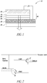
- FIG 1 shows a typical OLED (10) formed on a transparent substrate (20).
- An anode (30) is disposed on the transparent substrate (20) and is also transparent to allow the internally generated light to exit.
- the light-emitting layer takes the form of an organic emissive stack (40), which is disposed between the anode (30) and a cathode (50).
- the organic emissive stack (40) includes a thin film of electroluminescent chemical compounds (60) flanked by two charge injection layers (70 and 80, one for electron injection and one for hole injection).
- metal nanostructure-based transparent conductors represent an emerging class of transparent electrodes. Unlike the ITO, which is vacuum deposited on a substrate, metal nanostructure-based transparent conductors are formed by coating an ink formulation of metal nanowires on a substrate. The process addresses certain production limitations encountered by the ITO, and is particularly suitable for printing or coating on large area and/or flexible substrates.
- WO2010/129604A1 relates to providing reliable and durable conductive films, in particular, to conductive films exhibiting reliable electrical properties under intense and prolonged light exposure and capable of withstanding physical stresses. For this purpose, uniform silver nanowires are synthesized directly by the addition of an ionic additive to a reaction mixture.
- WO2010/082428A1 refers to a transparent electrode with improved surface smoothness, electrical conductivity and transparency.
- the transparent electrode comprises, on a transparent supporting body, a conductive layer that is composed of a metal nanowire layer and a conductive polymer layer, and is characterized in that the metal nanowire layer contains at least one substance selected from among crosslinked products of water-soluble polymers, crosslinked products of polymer latexes and cured products of curable resins.
- Self-assembled-monolayer-modified metals are used as anodes in the fabrication of top-emitting organic light-emitting diodes and an Ag anode modified by perfluoroalkanoate is shown to exhibit a luminous efficiency as high as 18 cdA -1 , superior to that of an Ag 2 O-based device.
- 92, 193313 (2008 ) relates to tuning the interface of a cathode in polymer solar cells by inserting a layer of ZnO/self-assembled monolayer (SAM) between a poly(3-hexylthiophene): [6,6]-phenyl-C61 butyric acid methyl ester bulk-heterojunction film and a metal cathode.
- SAM ZnO/self-assembled monolayer
- the light generation mechanism of the OLED is based on radiative recombination of excitons of electrically excited organic compound(s).
- LUMO lowest unoccupied molecular orbital
- HOMO highest occupied molecular orbital
- the process of withdrawing the electrons from the HOMO may also be described as injecting holes into the HOMO.
- Electrostatic forces bring the electrons and the holes toward each other and they recombine forming an exciton, an excided state of the electron bound to the hole.
- the excited state relaxes to the ground state of the electron, accompanied by emission of radiation, the frequency of which is in the visible region (380-800nm). The frequency of the radiation depends on the difference in energy between the HOMO and LUMO.
- FIG. 2 shows schematically an energy diagram of an OLED.
- the energy difference between the anode and HOMO represents an energy barrier (E h ) for the hole injection.
- the energy difference between the cathode and LUMO represents an energy barrier (E e ) for the electron injection.
- Work function of an anode corresponds to the minimum amount of energy needed to remove an electron from the surface of the anode (or cathode). As shown in Figure 2 , increasing the work function of the anode (e.g ., to the dashed line) decreases the energy barrier (E h ), thereby increasing the efficiency of the hole injection from the anode.
- the work function of a surface is strongly affected by the condition of the surface.
- the work function of ITO can be increased from 4.2eV to 4.8eV by oxygen plasma.
- oxygen plasma See, e.g., Wu, C. C. et al. Appl. Phys. Lett. 70(11):1348 (1997 ).
- Changing the work function of a material by absorption of a thin layer of a substance with an electrostatic dipole has also been reported. See, e.g., Gu, D. et al. J. Appl. Phys. 97:123710 (2005 ).
- a method for adjusting work function of a metal nanostructure-based conductive film comprising: providing a plurality of metal nanostructures, each metal nanostructure having an outer surface; and forming a dipole surface layer on the outer surface of the metal nanostructure, wherein the dipole surface layer includes a plurality of dipole ligands.
- forming the dipole surface layer on the outer surface of the metal nanostructure includes: forming an ink composition that comprises the plurality of metal nanostructures and the plurality of dipole ligand, and coating the ink composition on a substrate to provide the conductive film.
- adjusting work function includes increasing the work function by about 0.8-1.2 eV as compared to a conductive film form of metal nanostructures without a dipole surface layer.
- the dipole ligand is a polar molecule such as a surfactant.
- an anionic fluorosurfactant is used as the dipole ligand.
- the dipole ligand is lithium carboxylate anionic fluorosurfactant.
- an ink composition that comprises: a plurality of metal nanowires, and a dipole ligand, wherein the dipole ligand is present at about 10 -6 to 10 -4 moles per m 2 surface area of the metal nanostructures.
- the dipole ligand is present at about 10 -5 to 10 -4 moles per m 2 surface area of the metal nanostructures.
- the metal nanostructures are silver nanowires.
- the dipole ligand is an anionic fluorosurfactant.
- the anionic fluorosurfactant is a lithium carboxylate anionic fluorosurfactant.
- the ink composition may further comprise a surfactant, wherein a weight ratio of the plurality of the metal nanowires and the surfactant is in a range of 560:1 to 5:1.
- the ink composition may further comprise a viscosity modifier, such as hydroxypropyl methylcellulose (HPMC).
- a viscosity modifier such as hydroxypropyl methylcellulose (HPMC).
- a further embodiment provides an OLED device according to the claims comprising, a cathode, an anode, and an organic emissive stack disposed between the cathode and the anode, wherein the anode includes a conductive film of a plurality of metal nanostructures, each metal nanostructure having an outer surface and a dipole surface layer disposed on the outer surface, and wherein the dipole surface layer includes a plurality of dipole ligands.
- Described herein are methods for adjusting work function of nanostructure-based transparent conductor.
- the methods are directed to increasing the work function of a metal nanostructure-based transparent conductor (anode) in an OLED by modifying the surface of the metal nanostructures.
- anode a metal nanostructure-based transparent conductor
- the energy levels of the organic emissive stack and the anode are better aligned, thereby enhancing the quantum efficiency of the OLED and/or lowering the turn-on voltage.
- the overall power efficiency of the device is increased.
- one embodiment provides a method for adjusting work function of a metal nanostructure-based transparent conductor comprising: providing a plurality of metal nanostructures, each metal nanostructure having an outer surface; forming a dipole surface layer on the outer surface of the metal nanostructure, wherein the dipole surface layer includes a plurality of dipole ligands.
- a "dipole ligand” refers to a molecule or a particle that has a non-uniform distribution of positive and negative charges.
- the dipole ligand may have a permanent dipole.
- a polar molecule such as an ionic surfactant has a permanent dipole, which arises from substantially different electronegativity at one part of the molecule ( e.g. , the polar head of the surfactant) from another part of the molecule (e.g ., the lipophilic tail of the surfactant).
- the dipole ligand may also have an induced dipole (e.g., a polarizable molecule), in which case, the non-uniform distribution of the positive and negative charges are caused by a nearby molecule or particle that has a permanent dipole.
- an induced dipole e.g., a polarizable molecule
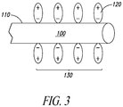
- Figure 3 schematically shows a nanowire (100) with an outer surface (110), on which dipole ligands (120) adsorb.
- Dipole ligands (120) in the surface region are subjected to orienting forces as a result of the anisotropic force field.
- Polar molecules e.g. permanent dipoles
- polarizable molecules may be polarized (induced dipoles) and oriented.
- the dipole ligands (100) are oriented in such a way that the negative end of the dipole ligand adsorbs to the surface (110), whereas the positive end of the dipole ligand points away from the surface (110).
- the preferential orientation causes the dipole ligands to form an array, typically of a single layer of the dipole ligands that are oriented in substantially the same direction.
- Such an array is called a surface dipole layer (130), with which an electric potential drop is associated. It is believed that the electric potential drop causes the increase of the work function of an anode formed by the metal nanowires.
- the dipole ligand may orient in such a way that the positive end of the dipole ligand adsorbs to the surface while the negative end points away from the surface.
- a surface dipole layer thus formed is associated with an electrical potential increase, which decreases the work function.
- forming the dipole surface layer on the outer surface of the metal nanostructure includes first forming an ink composition that comprises the metal nanostructures and the dipole ligand, followed by coating the ink composition on a substrate to provide a conductive film of interconnecting or networking nanostructures.
- the method described herein is therefore compatible with the solution-based approach to forming nanostructure-based conductive film.
- the dipole ligands adsorb to the outer surface of individual metal nanostructures in the liquid phase, and as the ink composition dries or cures on the substrate, a dipole surface layer is formed on each individual metal nanostructure.
- metal nanostructures in the presence of the dipole surface layer, are capable of forming conductive films in which the work function could increase by about 0.8eV-1.2eV as compared to conductive films made of the same metal nanostructures but without the dipole surface layer.
- the dipole ligand is an ionic surfactant molecule, which can be either an anionic (negatively charged) or cationic (positively charged) molecule.
- the surfactant molecule is an anionic fluorosurfactant.
- Non-limiting examples include ZONYL® FSA (lithium carboxylate anionic fluorosurfactant).
- Other dipole ligands with similar properties as ZONYL® FSA can be used, including, e.g., ZONYL® FSN, ZONYL® FSO, ZONYL® FSH (DuPont Chemicals, Wilmington, DE), and NOVECTM (3M, St. Paul, MN).
- the shift in work function is intrinsic to the material depending on the strength of the dipole moment.
- the dipole ligand can be added directly into an ink composition that comprises metal nanostructures. It is important that the dipole ligand is in sufficient amount relative to the metal nanostructures to form a dipole surface layer on each metal nanostructure. In various embodiments, the dipole ligand is present at about 10 -6 to 10 -4 moles per m 2 surface area of the metal nanostructures. In further embodiments, the dipole ligand is present at about 10 -5 to 10 -4 moles per m 2 surface area of the metal nanostructures.
- a surfactant is not necessarily a dipole ligand, as defined. While non-ionic surfactants can function as conventional surfactants by adsorbing on the nanostructures by static interaction (as opposed to ionic interaction), they may not be capable of forming an array or monolayer. Even ionic surfactants, unless reaching a critical concentration threshold in the ink composition, may not be capable of forming an array or monolayer.
- one embodiment provides an ink composition that comprises a plurality of silver nanowires, a surfactant, a viscosity modifier, and a dipole ligand, wherein the dipole ligand is present at about 10 -6 to 10 -4 moles per m 2 surface area of the metal nanostructures. In further embodiments, the dipole ligand is present at about 10 -5 to 10 -4 moles per m 2 surface area of the metal nanostructures.
- the work function of the conductive film increases from a range of about 4.5eV - 4.7eV (without FSA) to a range of about 5.2eV - 5.4eV.
- an OLED device comprising, a cathode, an anode, and an organic emissive stack disposed between the cathode and the anode, wherein the anode includes a conductive film of a plurality of metal nanostructures, each metal nanostructure having an outer surface and a dipole surface layer disposed on the outer surface, and wherein the dipole surface layer includes a plurality of dipole ligands.
- the dipole ligands are present at 10 -6 to 10 -4 moles per m 2 surface area of the metal nanostructures. In further embodiments, the dipole ligand is present at about 10 -5 to 10 -4 moles per m 2 surface area of the metal nanostructures. In further embodiments, the dipole ligands are anionic surfactants. In further embodiments, the anode has a work function of 5.2-5.7 eV.
- metal nanostructures or “nanostructures” generally refer to electrically conductive nano-sized structures, at least one dimension of which is less than 500nm, more preferably, less than 250nm, 100nm, 50nm or 25nm.
- the nanostructures can be of any shape or geometry.
- Typical isotropic nanostructures include nanoparticles.
- the nanostructures are anisotropically shaped ( i.e., aspect ratio ⁇ 1).
- aspect ratio refers to the ratio between the length and the width (or diameter) of the nanostructure.
- the anisotropic nanostructure typically has a longitudinal axis along its length.
- Exemplary anisotropic nanostructures include nanowires and nanotubes, as defined herein.
- the nanostructures can be solid or hollow.
- Solid nanostructures include, for example, nanoparticles and nanowires.
- Nanowires thus refers to solid anisotropic nanostructures.
- each nanowire has an aspect ratio (length:diameter) of greater than 10, preferably greater than 50, and more preferably greater than 100.
- the nanowires are more than 500nm, more than 1 ⁇ m, or more than 10 ⁇ m long.
- Hollow nanostructures include, for example, nanotubes.
- the nanotube has an aspect ratio (length:diameter) of greater than 10, preferably greater than 50, and more preferably greater than 100.
- the nanotubes are more than 500nm, more than 1 ⁇ m, or more than 10 ⁇ m in length.
- the metal nanostructures can be formed of any electrically conductive metallic material.
- the metallic material can be an elemental metal (e.g., transition metals) or a metal compound (e.g ., metal oxide).
- the metallic material can also be a bimetallic material or a metal alloy, which comprises two or more types of metal. Suitable metals include, but are not limited to, silver, gold, copper, nickel, gold-plated silver, platinum and palladium.
- a conductive film is typically in a multi-film configuration, and at least includes a nanostructure layer coated on a substrate.
- the nanostructure layer is formed by depositing an ink composition (also referred to as "coating composition") comprising a liquid carrier and a plurality of metal nanostructures on the substrate.
- the nanostructure layer or film comprises nanostructures that are randomly distributed and interconnect with one another. As the number of the nanostructures reaches the percolation threshold, the thin film is electrically conductive.
- Other non-volatile components of the ink composition including, for example, one or more binders, surfactants and additional viscosity modifiers, may form part of the conductive film.
- the liquid carrier for the dispersion may be water, an alcohol, a ketone or a combination thereof.
- exemplary alcohols may include isopropanol (IPA), ethanol, diacetone alcohol (DAA) or a combination of IPA and DAA.
- exemplary ketones may include methyl ethyl ketone (MEK) and methyl propyl ketone (MPK).
- the surfactants serve to reduce aggregation of the nanostructures.
- suitable surfactants include fluorosurfactants such as ZONYL® surfactants, including ZONYL® FSN, ZONYL® FSO, ZONYL® FSA, ZONYL® FSH (DuPont Chemicals, Wilmington, DE), and NOVECTM (3M, St. Paul, MN).
- fluorosurfactants such as ZONYL® surfactants, including ZONYL® FSN, ZONYL® FSO, ZONYL® FSA, ZONYL® FSH (DuPont Chemicals, Wilmington, DE), and NOVECTM (3M, St. Paul, MN).
- Other exemplary surfactants include non-ionic surfactants based on alkylphenol ethoxylates.
- Preferred surfactants include, for example, octylphenol ethoxylates such as TRITONTM (x100, x114, x45), and nonylphenol ethoxylates such as TERGITOLTM (Dow Chemical Company, Midland MI).
- Further exemplary non-ionic surfactants include acetylenic-based surfactants such as DYNOL® (604, 607) (Air Products and Chemicals, Inc., Allentown, PA) and n-dodecyl ⁇ -D-maltoside.
- the surfactant may be the same as the dipole ligand. In other embodiments, the surfactant may be different from the dipole ligand and co-exist with the dipole ligand in the ink composition.
- the binder acts as a viscosity modifier in the ink composition and may affect the rheology of the same during the coating process.
- the binder also helps to immobilize the nanostructures on a substrate.
- suitable binders include hydroxypropyl methylcellulose (HPMC), methyl cellulose, xanthan gum, polyvinyl alcohol, carboxy methyl cellulose, and hydroxy ethyl cellulose.
- the weight ratio of the surfactant to the binder in the coating solution is preferably in the range of about 80:1 to about 0.01:1; the weight ratio of the binder to the conductive nanostructures is preferably in the range of about 5:1 to about 0.000625:1; and the weight ratio of the conductive nanostructures to the surfactant is preferably in the range of about 560:1 to about 5:1.
- the ratios of components of the coating solution may be modified depending on the substrate and the method of application used.
- the electrical conductivity of the conductive film is often measured by "sheet resistance," which is represented by Ohms/square (or “ohms/sq”).
- the sheet resistance is a function of at least the surface loading density, the size/shapes of the nanostructures, and the intrinsic electrical property of the nanostructure constituents.
- a thin film is considered conductive if it has a sheet resistance of no higher than 10 8 ohms/sq.
- the sheet resistance is no higher than 10 4 ohms/sq, 3,000 ohms/sq, 1,000 ohms/sq, 350 ohms/sq, or 100 ohms/sq.
- the sheet resistance of a conductive network formed by metal nanostructures is in the range of from 10 ohms/sq to 1000 ohms/sq, from 100 ohms/sq to 750 ohms/sq, 50 ohms/sq to 200 ohms/sq, from 100 ohms/sq to 500 ohms/sq, from 100 ohms/sq to 250 ohms/sq, 10 ohms/sq to 200 ohms/sq, from 10 ohms/sq to 50 ohms/sq, or from 1 ohms/sq to 10 ohms/sq.
- the sheet resistance is typically less than 1000 ohms/sq, less than 500 ohms/sq, less than 100 ohms/sq, less than 50 ohms/square, less than 20 ohms/square, or less than 10 ohms/square.
- the nanostructure-based transparent conductors have high light transmission in the visible region (400nm-700nm).
- the transparent conductor is considered optically clear when the light transmission is more than 70%, or more typically more than 85% in the visible region. More preferably, the light transmission is more than 90%, more than 93%, or more than 95%.
- a conductive film is optically transparent (e.g ., more than 70% in transmission).
- transparent conductor; transparent conductive film, layer or coating; conductive film, layer or coating; and transparent electrode are used interchangeably.
- the substrate supports the nanostructure layer.
- the substrate is the support on which the ink composition is directly coated to form the nanostructure film, as defined herein.
- an intermediate layer i.e., an undercoat
- an undercoat is coated on the substrate before the ink composition is coated.
- the substrate can be rigid or flexible.
- rigid substrates include glass, polycarbonates, acrylics, and the like.
- flexible substrates include, but are not limited to: polyesters (e.g ., polyethylene terephthalate (PET), polyester naphthalate, and polycarbonate), polyolefins (e.g ., linear, branched, and cyclic polyolefins), polyvinyls (e.g.
- polyvinyl chloride polyvinylidene chloride, polyvinyl acetals, polystyrene, polyacrylates, and the like
- cellulose ester bases e.g., cellulose triacetate, and cellulose acetate
- polysulphones such as polyethersulphone, polyimides, silicones, and other conventional polymeric films.
- Silver nanowires were synthesized by the reduction of silver nitrate dissolved in ethylene glycol in the presence of poly(vinyl pyrrolidone) (PVP) following the "polyol” method described in, e.g., Y. Sun, B. Gates, B. Mayers, & Y. Xia, "Crystalline silver nanowires by soft solution processing," Nanoletters 2(2):165-168, 2002 .
- a modified polyol method described in co-pending and co-owned U.S. Patent Application No. 11/766,552 , produces more uniform silver nanowires at higher yields than does the conventional "polyol” method. Resulting nanowires primarily had lengths from about 13 ⁇ m to about 17 ⁇ m and diameters from about 25-45nm.
- a standard coating composition for depositing metal nanowires comprises, by weight, from 0.0025% to 0.1% surfactant (e.g ., a preferred range is from 0.0025% to 0.05% for the non-ionic surfactant ZONYL® FSO-100), from 0.02% to 4% viscosity modifier (e.g., a preferred range is 0.02% to 0.5% for hydroxypropyl methylcellulose (HPMC), from 94.5% to 99.0% solvent, and from 0.05% to 1.4% metal nanowires.
- This standard coating solution was used to form a reference film (S1), i.e., one without any dipole ligand.
- ZONYL® FSA was added to the standard coating composition.
- the silver nanowire:FSA ratio (by weight) was 1:0.7. This dispersion was used to make films for samples S2 and S3 of Example 4.
- the weight ratio of the silver nanowires and FSA can also be 1:0.1 to 1:1.
- the coating composition can be prepared based on a desired concentration of the nanowires, which is an index of the loading density of the final conductive film formed on the substrate.
- the coating composition can be deposited on a substrate according to, for example, the methods described in co-pending U.S. Patent Application No. 11/504,822 .
- deposition techniques can be employed, e.g ., sedimentation flow metered by a narrow channel, die flow, flow on an incline, slit coating, gravure coating, microgravure coating, bead coating, dip coating, slot die coating, and the like.
- Printing techniques can also be used to directly print an ink composition onto a substrate with or without a pattern.
- inkjet, flexoprinting and screen printing can be employed. It is further understood that the viscosity and shear behavior of the fluid as well as the interactions between the nanowires may affect the distribution and interconnectivity of the nanowires deposited.
- the Work function may be measured by an absolute scan with tip tracking.
- the absolute scan is a scan of approximate dimensions of 6x6 cm 2 conducted with a 2mm diameter Kelvin probe tip.
- the tip Work Function (WF) has been determined with reference to a pristine gold surface, the work function of which is 5.10eV.
- the scan may be performed at a constant tip to sample spacing, i.e., tracking, to ensure accurate comparison with the same tip on different samples.
- Both samples S2 and S3 were measured with Kelvin probe.
- SI-S3 Three samples of conductive films were prepared (SI-S3) according to the method described in Example 2. Each sample was 15 x 15 mm 2 . The samples were affixed to the sample holder with a conductive tape. S1 did not contain any FSA (dipole ligand) and was used as reference.
- the work function data has standard deviations in the 20-100 meV range, which is consistent with macroscopic work function measurements on real surfaces, i.e., surfaces that contain modest inhomogeneity such as scratches.
- the surfaces were well prepared, i.e., clean and free from fingerprints. The surfaces were further protected by lint-free tissue.
- the standard deviation was expected to be less than 20meV.
- the work function data of these samples are shown in Table 1 below.
- the data are the mean WF across the whole scan area ( e.g., 8 x 8 mm 2 ) and the standard deviation. These two values serve to differentiate between a homogeneous surface and one exhibiting significant artifacts.
- the work function data are smoothed.
- conductive films e.g., S1
- S1 conductive films formed of metal nanostructures without a dipole surface layer
- S2 work function of metal nanostructures without a dipole surface layer
- the work function of S2-S3 increased by about 0.8 - 1.2 eV.
- the work function distribution on a given conducive film is substantially uniform.
- Table 1 Samples Work Function(eV) Standard Deviation (eV) S1 4.5-4.7 S2 5.707 0.018 S3 5.540 0.085
Landscapes
- Chemical & Material Sciences (AREA)
- Physics & Mathematics (AREA)
- Engineering & Computer Science (AREA)
- Materials Engineering (AREA)
- Life Sciences & Earth Sciences (AREA)
- Nanotechnology (AREA)
- General Physics & Mathematics (AREA)
- Optics & Photonics (AREA)
- Organic Chemistry (AREA)
- Wood Science & Technology (AREA)
- Spectroscopy & Molecular Physics (AREA)
- Dispersion Chemistry (AREA)
- Composite Materials (AREA)
- Condensed Matter Physics & Semiconductors (AREA)
- Crystallography & Structural Chemistry (AREA)
- Analytical Chemistry (AREA)
- General Health & Medical Sciences (AREA)
- Immunology (AREA)
- Biochemistry (AREA)
- Pathology (AREA)
- Health & Medical Sciences (AREA)
- Plasma & Fusion (AREA)
- Chemical Kinetics & Catalysis (AREA)
- Inks, Pencil-Leads, Or Crayons (AREA)
- Electroluminescent Light Sources (AREA)
- Conductive Materials (AREA)
- Chemically Coating (AREA)
- Other Surface Treatments For Metallic Materials (AREA)
Applications Claiming Priority (2)
| Application Number | Priority Date | Filing Date | Title |
|---|---|---|---|
| US201161449519P | 2011-03-04 | 2011-03-04 | |
| PCT/US2012/027541 WO2012122034A1 (en) | 2011-03-04 | 2012-03-02 | Method of tuning work function of metal nanostructure-based transparent conductor |
Publications (2)
| Publication Number | Publication Date |
|---|---|
| EP2681780A1 EP2681780A1 (en) | 2014-01-08 |
| EP2681780B1 true EP2681780B1 (en) | 2018-11-28 |
Family
ID=45888479
Family Applications (1)
| Application Number | Title | Priority Date | Filing Date |
|---|---|---|---|
| EP12710827.2A Not-in-force EP2681780B1 (en) | 2011-03-04 | 2012-03-02 | Method of tuning work function of metal nanostructure-based transparent conductor |
Country Status (8)
Families Citing this family (13)
| Publication number | Priority date | Publication date | Assignee | Title |
|---|---|---|---|---|
| US9920207B2 (en) | 2012-06-22 | 2018-03-20 | C3Nano Inc. | Metal nanostructured networks and transparent conductive material |
| US10029916B2 (en) | 2012-06-22 | 2018-07-24 | C3Nano Inc. | Metal nanowire networks and transparent conductive material |
| US10020807B2 (en) | 2013-02-26 | 2018-07-10 | C3Nano Inc. | Fused metal nanostructured networks, fusing solutions with reducing agents and methods for forming metal networks |
| JP6201345B2 (ja) * | 2013-03-07 | 2017-09-27 | 三菱マテリアル株式会社 | Ito粒子を製造する方法 |
| JP2014224199A (ja) * | 2013-05-16 | 2014-12-04 | Dowaエレクトロニクス株式会社 | 銀ナノワイヤインクの製造方法および銀ナノワイヤインク |
| FR3011973B1 (fr) | 2013-10-10 | 2016-01-01 | Commissariat Energie Atomique | Materiau multicouches comprenant des nanofils metalliques et un polymere non conducteur electriquement |
| US11274223B2 (en) | 2013-11-22 | 2022-03-15 | C3 Nano, Inc. | Transparent conductive coatings based on metal nanowires and polymer binders, solution processing thereof, and patterning approaches |
| US11343911B1 (en) | 2014-04-11 | 2022-05-24 | C3 Nano, Inc. | Formable transparent conductive films with metal nanowires |
| US9183968B1 (en) | 2014-07-31 | 2015-11-10 | C3Nano Inc. | Metal nanowire inks for the formation of transparent conductive films with fused networks |
| KR102212159B1 (ko) * | 2014-11-05 | 2021-02-05 | 캄브리오스 필름 솔루션스 코포레이션 | 은 나노와이어-기반 투명 전도성 필름을 형성하기 위한 아이오다이드 첨가제를 갖는 단쇄 플루오로계면활성제 |
| KR102685407B1 (ko) * | 2019-08-02 | 2024-07-18 | 삼성디스플레이 주식회사 | 발광 소자, 이를 포함하는 표시 장치 및 표시 장치 제조 방법 |
| CN110739097B (zh) * | 2019-11-07 | 2021-07-16 | 浙江大学 | 功函数可调的银纳米线复合透明导电薄膜的制备方法 |
| FR3104173B1 (fr) | 2019-12-06 | 2023-07-21 | Centre Nat Rech Scient | : Procédé de production de nanoclusters de silicium et/ou germanium présentant un moment dipolaire électrique et/ou magnétique permanent |
Citations (1)
| Publication number | Priority date | Publication date | Assignee | Title |
|---|---|---|---|---|
| WO2010082428A1 (ja) * | 2009-01-19 | 2010-07-22 | コニカミノルタホールディングス株式会社 | 透明電極、その製造方法及び有機エレクトロルミネッセンス素子 |
Family Cites Families (14)
| Publication number | Priority date | Publication date | Assignee | Title |
|---|---|---|---|---|
| JP2004127562A (ja) * | 2002-09-30 | 2004-04-22 | Tokai Rubber Ind Ltd | 有機エレクトロルミネッセンス素子用透明電極およびそれを用いてなる有機エレクトロルミネッセンス素子 |
| US8563133B2 (en) * | 2004-06-08 | 2013-10-22 | Sandisk Corporation | Compositions and methods for modulation of nanostructure energy levels |
| US7776758B2 (en) * | 2004-06-08 | 2010-08-17 | Nanosys, Inc. | Methods and devices for forming nanostructure monolayers and devices including such monolayers |
| US7635858B2 (en) * | 2005-08-10 | 2009-12-22 | Au Optronics Corporation | Organic light-emitting device with improved layer conductivity distribution |
| KR20120128155A (ko) * | 2005-08-12 | 2012-11-26 | 캄브리오스 테크놀로지즈 코포레이션 | 나노와이어 기반의 투명 도전체 |
| JP2007149577A (ja) * | 2005-11-30 | 2007-06-14 | Alps Electric Co Ltd | 発光装置 |
| TWI397446B (zh) | 2006-06-21 | 2013-06-01 | Cambrios Technologies Corp | 控制奈米結構形成及形狀之方法 |
| KR101545219B1 (ko) * | 2006-10-12 | 2015-08-18 | 캄브리오스 테크놀로지즈 코포레이션 | 나노와이어 기반의 투명 도전체 및 그의 응용 |
| KR101184782B1 (ko) * | 2008-02-15 | 2012-09-20 | 쇼와 덴코 가부시키가이샤 | 전극의 표면 처리 방법 및 전극 및 유기 전계 발광 소자의 제조 방법 |
| US8323744B2 (en) * | 2009-01-09 | 2012-12-04 | The Board Of Trustees Of The Leland Stanford Junior University | Systems, methods, devices and arrangements for nanowire meshes |
| US20110024159A1 (en) * | 2009-05-05 | 2011-02-03 | Cambrios Technologies Corporation | Reliable and durable conductive films comprising metal nanostructures |
| SG175853A1 (en) * | 2009-05-05 | 2011-12-29 | Cambrios Technologies Corp | Reliable and durable conductive films comprising metal nanostructures |
| EP2539943B1 (en) * | 2010-02-24 | 2021-01-06 | Cambrios Film Solutions Corporation | Nanowire-based transparent conductors and methods of patterning same |
| US9244012B2 (en) * | 2011-09-26 | 2016-01-26 | University Of Maryland, Baltimore County | Enhanced luminescence from nanopolished surfaces and plate wells |
-
2012
- 2012-03-02 SG SG2013065818A patent/SG193253A1/en unknown
- 2012-03-02 CN CN201280011724.5A patent/CN103503191A/zh active Pending
- 2012-03-02 EP EP12710827.2A patent/EP2681780B1/en not_active Not-in-force
- 2012-03-02 US US13/411,154 patent/US8723216B2/en active Active
- 2012-03-02 WO PCT/US2012/027541 patent/WO2012122034A1/en active Application Filing
- 2012-03-02 JP JP2013556911A patent/JP2014511551A/ja active Pending
- 2012-03-02 KR KR1020137026283A patent/KR20140020957A/ko not_active Ceased
- 2012-03-03 TW TW101107221A patent/TWI577237B/zh not_active IP Right Cessation
Patent Citations (1)
| Publication number | Priority date | Publication date | Assignee | Title |
|---|---|---|---|---|
| WO2010082428A1 (ja) * | 2009-01-19 | 2010-07-22 | コニカミノルタホールディングス株式会社 | 透明電極、その製造方法及び有機エレクトロルミネッセンス素子 |
Non-Patent Citations (2)
| Title |
|---|
| CHUN-PEI CHO AND YU-TAI TAO: "Tuning of Metal Work Function with Organic Carboxylates and Its Application in Top-Emitting Electroluminescent Devices", LANGMUIR, AMERICAN CHEMICAL SOCIETY, US, vol. 23, no. 13, 19 June 2007 (2007-06-19), pages 7090 - 7095, XP002675351, ISSN: 0743-7463, [retrieved on 20070524], DOI: 10.1021/LA700648Z * |
| YIP HIN-LAP ET AL: "Self-assembled monolayer modified ZnO/metal bilayer cathodes for polymer/fullerene bulk-heterojunction solar cells", APPLIED PHYSICS LETTERS, A I P PUBLISHING LLC, US, vol. 92, no. 19, 16 May 2008 (2008-05-16), pages 193313 - 193313, XP012106937, ISSN: 0003-6951, DOI: 10.1063/1.2919524 * |
Also Published As
| Publication number | Publication date |
|---|---|
| TW201242425A (en) | 2012-10-16 |
| US8723216B2 (en) | 2014-05-13 |
| TWI577237B (zh) | 2017-04-01 |
| WO2012122034A1 (en) | 2012-09-13 |
| US20120223358A1 (en) | 2012-09-06 |
| JP2014511551A (ja) | 2014-05-15 |
| SG193253A1 (en) | 2013-10-30 |
| CN103503191A (zh) | 2014-01-08 |
| KR20140020957A (ko) | 2014-02-19 |
| EP2681780A1 (en) | 2014-01-08 |
Similar Documents
| Publication | Publication Date | Title |
|---|---|---|
| EP2681780B1 (en) | Method of tuning work function of metal nanostructure-based transparent conductor | |
| US10964890B2 (en) | Opto-electrical devices incorporating metal nanowires | |
| TWI499602B (zh) | 有機電子裝置、組合物及方法 | |
| US20120104374A1 (en) | Coating compositions for forming nanocomposite films | |
| US20160060468A1 (en) | Aqueous compositions, methods of producing conductive thin films using the same, conductive thin films produced thereby, and electronic devices including the same | |
| CN107852793B (zh) | 有机薄膜层叠体及有机电致发光元件 | |
| US20090252967A1 (en) | Carbon nanotube transparent electrode and method of manufacturing the same | |
| Jiang et al. | Double-heterojunction nanorod light-emitting diodes with high efficiencies at high brightness using self-assembled monolayers | |
| US11508929B2 (en) | Conductor and method of manufacturing the same | |
| HK1190501B (en) | Method of tuning work function of metal nanostructure-based transparent conductor | |
| HK1190501A (en) | Method of tuning work function of metal nanostructure-based transparent conductor | |
| US8329505B2 (en) | Method for deposition of cathodes for polymer optoelectronic devices | |
| CN114686205A (zh) | 量子点材料的改性方法及改性的量子点材料、发光器件 | |
| US9755179B2 (en) | Conductor and method of manufacturing the same | |
| KR101956419B1 (ko) | 유기 발광 소자 및 그 제조 방법 | |
| KR102592869B1 (ko) | 질소-포함 방향족 헤테로 고리를 갖는 화합물을 포함하는 나노 박막, 이의 제조 방법, 및 이를 포함하는 복합 나노 박막 | |
| JPWO2020130021A1 (ja) | 電子デバイス及び電子デバイスの製造方法 |
Legal Events
| Date | Code | Title | Description |
|---|---|---|---|
| PUAI | Public reference made under article 153(3) epc to a published international application that has entered the european phase |
Free format text: ORIGINAL CODE: 0009012 |
|
| 17P | Request for examination filed |
Effective date: 20131004 |
|
| AK | Designated contracting states |
Kind code of ref document: A1 Designated state(s): AL AT BE BG CH CY CZ DE DK EE ES FI FR GB GR HR HU IE IS IT LI LT LU LV MC MK MT NL NO PL PT RO RS SE SI SK SM TR |
|
| DAX | Request for extension of the european patent (deleted) | ||
| REG | Reference to a national code |
Ref country code: HK Ref legal event code: DE Ref document number: 1190501 Country of ref document: HK |
|
| 17Q | First examination report despatched |
Effective date: 20160303 |
|
| STAA | Information on the status of an ep patent application or granted ep patent |
Free format text: STATUS: EXAMINATION IS IN PROGRESS |
|
| RAP1 | Party data changed (applicant data changed or rights of an application transferred) |
Owner name: CAM HOLDING CORPORATION |
|
| GRAP | Despatch of communication of intention to grant a patent |
Free format text: ORIGINAL CODE: EPIDOSNIGR1 |
|
| STAA | Information on the status of an ep patent application or granted ep patent |
Free format text: STATUS: GRANT OF PATENT IS INTENDED |
|
| RIC1 | Information provided on ipc code assigned before grant |
Ipc: G02F 1/1343 20060101ALI20180416BHEP Ipc: C09D 5/24 20060101ALI20180416BHEP Ipc: H05K 1/09 20060101ALI20180416BHEP Ipc: H01B 1/02 20060101ALI20180416BHEP Ipc: H01L 31/0224 20060101ALI20180416BHEP Ipc: H01L 51/44 20060101ALI20180416BHEP Ipc: H01L 51/52 20060101AFI20180416BHEP Ipc: H01L 51/10 20060101ALI20180416BHEP Ipc: B82Y 10/00 20110101ALI20180416BHEP Ipc: H01L 31/18 20060101ALI20180416BHEP Ipc: H01B 1/22 20060101ALI20180416BHEP |
|
| INTG | Intention to grant announced |
Effective date: 20180518 |
|
| RIC1 | Information provided on ipc code assigned before grant |
Ipc: H01L 51/52 20060101AFI20180507BHEP Ipc: H01B 1/02 20060101ALI20180507BHEP Ipc: H01L 51/44 20060101ALI20180507BHEP Ipc: H01B 1/22 20060101ALI20180507BHEP |
|
| GRAS | Grant fee paid |
Free format text: ORIGINAL CODE: EPIDOSNIGR3 |
|
| GRAJ | Information related to disapproval of communication of intention to grant by the applicant or resumption of examination proceedings by the epo deleted |
Free format text: ORIGINAL CODE: EPIDOSDIGR1 |
|
| GRAL | Information related to payment of fee for publishing/printing deleted |
Free format text: ORIGINAL CODE: EPIDOSDIGR3 |
|
| STAA | Information on the status of an ep patent application or granted ep patent |
Free format text: STATUS: EXAMINATION IS IN PROGRESS |
|
| GRAR | Information related to intention to grant a patent recorded |
Free format text: ORIGINAL CODE: EPIDOSNIGR71 |
|
| STAA | Information on the status of an ep patent application or granted ep patent |
Free format text: STATUS: GRANT OF PATENT IS INTENDED |
|
| GRAA | (expected) grant |
Free format text: ORIGINAL CODE: 0009210 |
|
| STAA | Information on the status of an ep patent application or granted ep patent |
Free format text: STATUS: THE PATENT HAS BEEN GRANTED |
|
| INTC | Intention to grant announced (deleted) | ||
| AK | Designated contracting states |
Kind code of ref document: B1 Designated state(s): AL AT BE BG CH CY CZ DE DK EE ES FI FR GB GR HR HU IE IS IT LI LT LU LV MC MK MT NL NO PL PT RO RS SE SI SK SM TR |
|
| INTG | Intention to grant announced |
Effective date: 20181022 |
|
| REG | Reference to a national code |
Ref country code: GB Ref legal event code: FG4D |
|
| REG | Reference to a national code |
Ref country code: CH Ref legal event code: EP |
|
| REG | Reference to a national code |
Ref country code: AT Ref legal event code: REF Ref document number: 1071260 Country of ref document: AT Kind code of ref document: T Effective date: 20181215 |
|
| REG | Reference to a national code |
Ref country code: DE Ref legal event code: R096 Ref document number: 602012054030 Country of ref document: DE |
|
| REG | Reference to a national code |
Ref country code: IE Ref legal event code: FG4D |
|
| RAP2 | Party data changed (patent owner data changed or rights of a patent transferred) |
Owner name: CAMBRIOS FILM SOLUTIONS CORPORATION |
|
| REG | Reference to a national code |
Ref country code: DE Ref legal event code: R081 Ref document number: 602012054030 Country of ref document: DE Owner name: CAMBRIOS FILM SOLUTIONS CORP., ROAD TOWN, VG Free format text: FORMER OWNER: CAM HOLDING CORP., ROAD TOWN, TORTOLA, VG |
|
| REG | Reference to a national code |
Ref country code: NL Ref legal event code: FP |
|
| REG | Reference to a national code |
Ref country code: LT Ref legal event code: MG4D |
|
| REG | Reference to a national code |
Ref country code: AT Ref legal event code: MK05 Ref document number: 1071260 Country of ref document: AT Kind code of ref document: T Effective date: 20181128 |
|
| PG25 | Lapsed in a contracting state [announced via postgrant information from national office to epo] |
Ref country code: LV Free format text: LAPSE BECAUSE OF FAILURE TO SUBMIT A TRANSLATION OF THE DESCRIPTION OR TO PAY THE FEE WITHIN THE PRESCRIBED TIME-LIMIT Effective date: 20181128 Ref country code: FI Free format text: LAPSE BECAUSE OF FAILURE TO SUBMIT A TRANSLATION OF THE DESCRIPTION OR TO PAY THE FEE WITHIN THE PRESCRIBED TIME-LIMIT Effective date: 20181128 Ref country code: LT Free format text: LAPSE BECAUSE OF FAILURE TO SUBMIT A TRANSLATION OF THE DESCRIPTION OR TO PAY THE FEE WITHIN THE PRESCRIBED TIME-LIMIT Effective date: 20181128 Ref country code: HR Free format text: LAPSE BECAUSE OF FAILURE TO SUBMIT A TRANSLATION OF THE DESCRIPTION OR TO PAY THE FEE WITHIN THE PRESCRIBED TIME-LIMIT Effective date: 20181128 Ref country code: NO Free format text: LAPSE BECAUSE OF FAILURE TO SUBMIT A TRANSLATION OF THE DESCRIPTION OR TO PAY THE FEE WITHIN THE PRESCRIBED TIME-LIMIT Effective date: 20190228 Ref country code: BG Free format text: LAPSE BECAUSE OF FAILURE TO SUBMIT A TRANSLATION OF THE DESCRIPTION OR TO PAY THE FEE WITHIN THE PRESCRIBED TIME-LIMIT Effective date: 20190228 Ref country code: AT Free format text: LAPSE BECAUSE OF FAILURE TO SUBMIT A TRANSLATION OF THE DESCRIPTION OR TO PAY THE FEE WITHIN THE PRESCRIBED TIME-LIMIT Effective date: 20181128 Ref country code: IS Free format text: LAPSE BECAUSE OF FAILURE TO SUBMIT A TRANSLATION OF THE DESCRIPTION OR TO PAY THE FEE WITHIN THE PRESCRIBED TIME-LIMIT Effective date: 20190328 Ref country code: ES Free format text: LAPSE BECAUSE OF FAILURE TO SUBMIT A TRANSLATION OF THE DESCRIPTION OR TO PAY THE FEE WITHIN THE PRESCRIBED TIME-LIMIT Effective date: 20181128 |
|
| PG25 | Lapsed in a contracting state [announced via postgrant information from national office to epo] |
Ref country code: SE Free format text: LAPSE BECAUSE OF FAILURE TO SUBMIT A TRANSLATION OF THE DESCRIPTION OR TO PAY THE FEE WITHIN THE PRESCRIBED TIME-LIMIT Effective date: 20181128 Ref country code: PT Free format text: LAPSE BECAUSE OF FAILURE TO SUBMIT A TRANSLATION OF THE DESCRIPTION OR TO PAY THE FEE WITHIN THE PRESCRIBED TIME-LIMIT Effective date: 20190328 Ref country code: GR Free format text: LAPSE BECAUSE OF FAILURE TO SUBMIT A TRANSLATION OF THE DESCRIPTION OR TO PAY THE FEE WITHIN THE PRESCRIBED TIME-LIMIT Effective date: 20190301 Ref country code: RS Free format text: LAPSE BECAUSE OF FAILURE TO SUBMIT A TRANSLATION OF THE DESCRIPTION OR TO PAY THE FEE WITHIN THE PRESCRIBED TIME-LIMIT Effective date: 20181128 Ref country code: AL Free format text: LAPSE BECAUSE OF FAILURE TO SUBMIT A TRANSLATION OF THE DESCRIPTION OR TO PAY THE FEE WITHIN THE PRESCRIBED TIME-LIMIT Effective date: 20181128 |
|
| PG25 | Lapsed in a contracting state [announced via postgrant information from national office to epo] |
Ref country code: CZ Free format text: LAPSE BECAUSE OF FAILURE TO SUBMIT A TRANSLATION OF THE DESCRIPTION OR TO PAY THE FEE WITHIN THE PRESCRIBED TIME-LIMIT Effective date: 20181128 Ref country code: PL Free format text: LAPSE BECAUSE OF FAILURE TO SUBMIT A TRANSLATION OF THE DESCRIPTION OR TO PAY THE FEE WITHIN THE PRESCRIBED TIME-LIMIT Effective date: 20181128 Ref country code: IT Free format text: LAPSE BECAUSE OF FAILURE TO SUBMIT A TRANSLATION OF THE DESCRIPTION OR TO PAY THE FEE WITHIN THE PRESCRIBED TIME-LIMIT Effective date: 20181128 Ref country code: DK Free format text: LAPSE BECAUSE OF FAILURE TO SUBMIT A TRANSLATION OF THE DESCRIPTION OR TO PAY THE FEE WITHIN THE PRESCRIBED TIME-LIMIT Effective date: 20181128 |
|
| REG | Reference to a national code |
Ref country code: DE Ref legal event code: R097 Ref document number: 602012054030 Country of ref document: DE |
|
| PG25 | Lapsed in a contracting state [announced via postgrant information from national office to epo] |
Ref country code: SM Free format text: LAPSE BECAUSE OF FAILURE TO SUBMIT A TRANSLATION OF THE DESCRIPTION OR TO PAY THE FEE WITHIN THE PRESCRIBED TIME-LIMIT Effective date: 20181128 Ref country code: SK Free format text: LAPSE BECAUSE OF FAILURE TO SUBMIT A TRANSLATION OF THE DESCRIPTION OR TO PAY THE FEE WITHIN THE PRESCRIBED TIME-LIMIT Effective date: 20181128 Ref country code: EE Free format text: LAPSE BECAUSE OF FAILURE TO SUBMIT A TRANSLATION OF THE DESCRIPTION OR TO PAY THE FEE WITHIN THE PRESCRIBED TIME-LIMIT Effective date: 20181128 Ref country code: RO Free format text: LAPSE BECAUSE OF FAILURE TO SUBMIT A TRANSLATION OF THE DESCRIPTION OR TO PAY THE FEE WITHIN THE PRESCRIBED TIME-LIMIT Effective date: 20181128 |
|
| PLBE | No opposition filed within time limit |
Free format text: ORIGINAL CODE: 0009261 |
|
| STAA | Information on the status of an ep patent application or granted ep patent |
Free format text: STATUS: NO OPPOSITION FILED WITHIN TIME LIMIT |
|
| PG25 | Lapsed in a contracting state [announced via postgrant information from national office to epo] |
Ref country code: SI Free format text: LAPSE BECAUSE OF FAILURE TO SUBMIT A TRANSLATION OF THE DESCRIPTION OR TO PAY THE FEE WITHIN THE PRESCRIBED TIME-LIMIT Effective date: 20181128 Ref country code: MC Free format text: LAPSE BECAUSE OF FAILURE TO SUBMIT A TRANSLATION OF THE DESCRIPTION OR TO PAY THE FEE WITHIN THE PRESCRIBED TIME-LIMIT Effective date: 20181128 |
|
| REG | Reference to a national code |
Ref country code: CH Ref legal event code: PL |
|
| 26N | No opposition filed |
Effective date: 20190829 |
|
| PG25 | Lapsed in a contracting state [announced via postgrant information from national office to epo] |
Ref country code: LU Free format text: LAPSE BECAUSE OF NON-PAYMENT OF DUE FEES Effective date: 20190302 |
|
| REG | Reference to a national code |
Ref country code: BE Ref legal event code: MM Effective date: 20190331 |
|
| PG25 | Lapsed in a contracting state [announced via postgrant information from national office to epo] |
Ref country code: IE Free format text: LAPSE BECAUSE OF NON-PAYMENT OF DUE FEES Effective date: 20190302 Ref country code: LI Free format text: LAPSE BECAUSE OF NON-PAYMENT OF DUE FEES Effective date: 20190331 Ref country code: CH Free format text: LAPSE BECAUSE OF NON-PAYMENT OF DUE FEES Effective date: 20190331 |
|
| PG25 | Lapsed in a contracting state [announced via postgrant information from national office to epo] |
Ref country code: BE Free format text: LAPSE BECAUSE OF NON-PAYMENT OF DUE FEES Effective date: 20190331 |
|
| PG25 | Lapsed in a contracting state [announced via postgrant information from national office to epo] |
Ref country code: TR Free format text: LAPSE BECAUSE OF FAILURE TO SUBMIT A TRANSLATION OF THE DESCRIPTION OR TO PAY THE FEE WITHIN THE PRESCRIBED TIME-LIMIT Effective date: 20181128 |
|
| PG25 | Lapsed in a contracting state [announced via postgrant information from national office to epo] |
Ref country code: MT Free format text: LAPSE BECAUSE OF NON-PAYMENT OF DUE FEES Effective date: 20190302 |
|
| PGFP | Annual fee paid to national office [announced via postgrant information from national office to epo] |
Ref country code: FR Payment date: 20210112 Year of fee payment: 10 Ref country code: NL Payment date: 20210212 Year of fee payment: 10 |
|
| PG25 | Lapsed in a contracting state [announced via postgrant information from national office to epo] |
Ref country code: CY Free format text: LAPSE BECAUSE OF FAILURE TO SUBMIT A TRANSLATION OF THE DESCRIPTION OR TO PAY THE FEE WITHIN THE PRESCRIBED TIME-LIMIT Effective date: 20181128 |
|
| PGFP | Annual fee paid to national office [announced via postgrant information from national office to epo] |
Ref country code: GB Payment date: 20210217 Year of fee payment: 10 Ref country code: DE Payment date: 20210216 Year of fee payment: 10 |
|
| PG25 | Lapsed in a contracting state [announced via postgrant information from national office to epo] |
Ref country code: HU Free format text: LAPSE BECAUSE OF FAILURE TO SUBMIT A TRANSLATION OF THE DESCRIPTION OR TO PAY THE FEE WITHIN THE PRESCRIBED TIME-LIMIT; INVALID AB INITIO Effective date: 20120302 |
|
| PG25 | Lapsed in a contracting state [announced via postgrant information from national office to epo] |
Ref country code: MK Free format text: LAPSE BECAUSE OF FAILURE TO SUBMIT A TRANSLATION OF THE DESCRIPTION OR TO PAY THE FEE WITHIN THE PRESCRIBED TIME-LIMIT Effective date: 20181128 |
|
| REG | Reference to a national code |
Ref country code: DE Ref legal event code: R119 Ref document number: 602012054030 Country of ref document: DE |
|
| REG | Reference to a national code |
Ref country code: NL Ref legal event code: MM Effective date: 20220401 |
|
| GBPC | Gb: european patent ceased through non-payment of renewal fee |
Effective date: 20220302 |
|
| PG25 | Lapsed in a contracting state [announced via postgrant information from national office to epo] |
Ref country code: NL Free format text: LAPSE BECAUSE OF NON-PAYMENT OF DUE FEES Effective date: 20220401 Ref country code: GB Free format text: LAPSE BECAUSE OF NON-PAYMENT OF DUE FEES Effective date: 20220302 Ref country code: FR Free format text: LAPSE BECAUSE OF NON-PAYMENT OF DUE FEES Effective date: 20220331 Ref country code: DE Free format text: LAPSE BECAUSE OF NON-PAYMENT OF DUE FEES Effective date: 20221001 |