EP2675935B1 - Verfahren zum herstellen eines dünnfilms aus blei-zirkonat-titanat - Google Patents
Verfahren zum herstellen eines dünnfilms aus blei-zirkonat-titanat Download PDFInfo
- Publication number
- EP2675935B1 EP2675935B1 EP12705252.0A EP12705252A EP2675935B1 EP 2675935 B1 EP2675935 B1 EP 2675935B1 EP 12705252 A EP12705252 A EP 12705252A EP 2675935 B1 EP2675935 B1 EP 2675935B1
- Authority
- EP
- European Patent Office
- Prior art keywords
- thin film
- lead
- zirconium
- titanium
- deposition rate
- Prior art date
- Legal status (The legal status is an assumption and is not a legal conclusion. Google has not performed a legal analysis and makes no representation as to the accuracy of the status listed.)
- Active
Links
Images

Classifications
-
- H—ELECTRICITY
- H10—SEMICONDUCTOR DEVICES; ELECTRIC SOLID-STATE DEVICES NOT OTHERWISE PROVIDED FOR
- H10N—ELECTRIC SOLID-STATE DEVICES NOT OTHERWISE PROVIDED FOR
- H10N30/00—Piezoelectric or electrostrictive devices
- H10N30/80—Constructional details
- H10N30/85—Piezoelectric or electrostrictive active materials
- H10N30/853—Ceramic compositions
- H10N30/8548—Lead-based oxides
- H10N30/8554—Lead-zirconium titanate [PZT] based
-
- C—CHEMISTRY; METALLURGY
- C23—COATING METALLIC MATERIAL; COATING MATERIAL WITH METALLIC MATERIAL; CHEMICAL SURFACE TREATMENT; DIFFUSION TREATMENT OF METALLIC MATERIAL; COATING BY VACUUM EVAPORATION, BY SPUTTERING, BY ION IMPLANTATION OR BY CHEMICAL VAPOUR DEPOSITION, IN GENERAL; INHIBITING CORROSION OF METALLIC MATERIAL OR INCRUSTATION IN GENERAL
- C23C—COATING METALLIC MATERIAL; COATING MATERIAL WITH METALLIC MATERIAL; SURFACE TREATMENT OF METALLIC MATERIAL BY DIFFUSION INTO THE SURFACE, BY CHEMICAL CONVERSION OR SUBSTITUTION; COATING BY VACUUM EVAPORATION, BY SPUTTERING, BY ION IMPLANTATION OR BY CHEMICAL VAPOUR DEPOSITION, IN GENERAL
- C23C14/00—Coating by vacuum evaporation, by sputtering or by ion implantation of the coating forming material
- C23C14/06—Coating by vacuum evaporation, by sputtering or by ion implantation of the coating forming material characterised by the coating material
- C23C14/08—Oxides
- C23C14/088—Oxides of the type ABO3 with A representing alkali, alkaline earth metal or Pb and B representing a refractory or rare earth metal
-
- C—CHEMISTRY; METALLURGY
- C23—COATING METALLIC MATERIAL; COATING MATERIAL WITH METALLIC MATERIAL; CHEMICAL SURFACE TREATMENT; DIFFUSION TREATMENT OF METALLIC MATERIAL; COATING BY VACUUM EVAPORATION, BY SPUTTERING, BY ION IMPLANTATION OR BY CHEMICAL VAPOUR DEPOSITION, IN GENERAL; INHIBITING CORROSION OF METALLIC MATERIAL OR INCRUSTATION IN GENERAL
- C23C—COATING METALLIC MATERIAL; COATING MATERIAL WITH METALLIC MATERIAL; SURFACE TREATMENT OF METALLIC MATERIAL BY DIFFUSION INTO THE SURFACE, BY CHEMICAL CONVERSION OR SUBSTITUTION; COATING BY VACUUM EVAPORATION, BY SPUTTERING, BY ION IMPLANTATION OR BY CHEMICAL VAPOUR DEPOSITION, IN GENERAL
- C23C14/00—Coating by vacuum evaporation, by sputtering or by ion implantation of the coating forming material
- C23C14/0021—Reactive sputtering or evaporation
- C23C14/0036—Reactive sputtering
-
- C—CHEMISTRY; METALLURGY
- C23—COATING METALLIC MATERIAL; COATING MATERIAL WITH METALLIC MATERIAL; CHEMICAL SURFACE TREATMENT; DIFFUSION TREATMENT OF METALLIC MATERIAL; COATING BY VACUUM EVAPORATION, BY SPUTTERING, BY ION IMPLANTATION OR BY CHEMICAL VAPOUR DEPOSITION, IN GENERAL; INHIBITING CORROSION OF METALLIC MATERIAL OR INCRUSTATION IN GENERAL
- C23C—COATING METALLIC MATERIAL; COATING MATERIAL WITH METALLIC MATERIAL; SURFACE TREATMENT OF METALLIC MATERIAL BY DIFFUSION INTO THE SURFACE, BY CHEMICAL CONVERSION OR SUBSTITUTION; COATING BY VACUUM EVAPORATION, BY SPUTTERING, BY ION IMPLANTATION OR BY CHEMICAL VAPOUR DEPOSITION, IN GENERAL
- C23C14/00—Coating by vacuum evaporation, by sputtering or by ion implantation of the coating forming material
- C23C14/22—Coating by vacuum evaporation, by sputtering or by ion implantation of the coating forming material characterised by the process of coating
- C23C14/34—Sputtering
- C23C14/3464—Sputtering using more than one target
-
- H—ELECTRICITY
- H10—SEMICONDUCTOR DEVICES; ELECTRIC SOLID-STATE DEVICES NOT OTHERWISE PROVIDED FOR
- H10N—ELECTRIC SOLID-STATE DEVICES NOT OTHERWISE PROVIDED FOR
- H10N15/00—Thermoelectric devices without a junction of dissimilar materials; Thermomagnetic devices, e.g. using the Nernst-Ettingshausen effect
- H10N15/10—Thermoelectric devices using thermal change of the dielectric constant, e.g. working above and below the Curie point
- H10N15/15—Thermoelectric active materials
-
- H—ELECTRICITY
- H10—SEMICONDUCTOR DEVICES; ELECTRIC SOLID-STATE DEVICES NOT OTHERWISE PROVIDED FOR
- H10N—ELECTRIC SOLID-STATE DEVICES NOT OTHERWISE PROVIDED FOR
- H10N30/00—Piezoelectric or electrostrictive devices
- H10N30/01—Manufacture or treatment
- H10N30/07—Forming of piezoelectric or electrostrictive parts or bodies on an electrical element or another base
- H10N30/074—Forming of piezoelectric or electrostrictive parts or bodies on an electrical element or another base by depositing piezoelectric or electrostrictive layers, e.g. aerosol or screen printing
- H10N30/076—Forming of piezoelectric or electrostrictive parts or bodies on an electrical element or another base by depositing piezoelectric or electrostrictive layers, e.g. aerosol or screen printing by vapour phase deposition
-
- H—ELECTRICITY
- H10—SEMICONDUCTOR DEVICES; ELECTRIC SOLID-STATE DEVICES NOT OTHERWISE PROVIDED FOR
- H10P—GENERIC PROCESSES OR APPARATUS FOR THE MANUFACTURE OR TREATMENT OF DEVICES COVERED BY CLASS H10
- H10P14/00—Formation of materials, e.g. in the shape of layers or pillars
- H10P14/60—Formation of materials, e.g. in the shape of layers or pillars of insulating materials
- H10P14/63—Formation of materials, e.g. in the shape of layers or pillars of insulating materials characterised by the formation processes
- H10P14/6326—Deposition processes
- H10P14/6328—Deposition from the gas or vapour phase
- H10P14/6329—Deposition from the gas or vapour phase using physical ablation of a target, e.g. physical vapour deposition or pulsed laser deposition
-
- H—ELECTRICITY
- H10—SEMICONDUCTOR DEVICES; ELECTRIC SOLID-STATE DEVICES NOT OTHERWISE PROVIDED FOR
- H10P—GENERIC PROCESSES OR APPARATUS FOR THE MANUFACTURE OR TREATMENT OF DEVICES COVERED BY CLASS H10
- H10P14/00—Formation of materials, e.g. in the shape of layers or pillars
- H10P14/60—Formation of materials, e.g. in the shape of layers or pillars of insulating materials
- H10P14/69—Inorganic materials
- H10P14/692—Inorganic materials composed of oxides, glassy oxides or oxide-based glasses
- H10P14/6938—Inorganic materials composed of oxides, glassy oxides or oxide-based glasses the material containing at least one metal element, e.g. metal oxides, metal oxynitrides or metal oxycarbides
- H10P14/69398—Inorganic materials composed of oxides, glassy oxides or oxide-based glasses the material containing at least one metal element, e.g. metal oxides, metal oxynitrides or metal oxycarbides the material having a perovskite structure, e.g. BaTiO3
Definitions
- the invention relates to a method for producing a thin film of lead-zirconate-titanate in a 111-oriented perovskite structure.
- a thin film made of lead zirconate titanate is used in electronic components, whereby the advantageous dielectric, pyroelectric and piezoelectric properties of lead zirconate titanate are used.
- electronic components are, for example, capacitors, pyrodetectors, piezo actuators or semiconductor memories.
- a first electrode layer is conventionally deposited on a substrate, the thin film made of lead-zirconate-titanate over it and, in turn, a second electrode layer over it.
- the lead zirconate titanate thin film is produced by a thin film process which is known to be a sputtering process, a CVD process, or a sol-gel process.
- a gas mixture of argon and oxygen is ionized in a vacuum by a high voltage to form a plasma.
- Lead, zirconium and titanium are each provided in the form of a target, the target being connected as the cathode and the substrate as the anode.
- atoms are knocked out of the target and deposited on the substrate to form the thin film.
- the substrate is conventionally a silicon wafer, which is manufactured like a membrane in subsequent processing steps.
- platinum is suitable as the electrode material, since it can withstand the deposition conditions of lead-zirconate-titanate undamaged at high substrate temperatures and in an oxygen-containing atmosphere during sputtering and no diffusion occurs in the thin film, which could lead to a disadvantageously changed composition and thus to a deterioration in the properties of the thin film.
- the expression of the pyroelectric property of the thin film depends on the composition of the thin film with lead, zirconium and titanium.
- the thin film is produced in a self-polarized manner, in particular with a thickness of 0.2 to 3 ⁇ m, using the sputtering method.
- the sputtering process is to be carried out with a total deposition rate of lead, zirconium and titanium between 1 and 7 nm / min, whereby the thin film with the 111-oriented perovskite structure is formed and the thin film has a pyroelectric coefficient between 2 ⁇ 10 -9 to 5 ⁇ 10 -4 C / m 2 .
- the disadvantage of this sputtering process is that the total deposition rate of lead, zirconium and titanium of 1 to 7 nm / min represents only a low production speed of the thin film, so that only a low throughput rate of thin films can be achieved with this sputtering process, which makes it economically viable this sputtering method for forming the thin film is small.
- the object of the invention is to provide a method for producing a thin film of lead zirconate titanate in a 111-oriented perovskite structure, the method being able to achieve a high throughput rate of thin films although the thin film has a high pyroelectric coefficient.
- the sputtering of lead, zirconium and titanium from the respective targets onto the substrate is preferably confocal and / or simultaneous.
- the deposition rate of lead is chosen such that the atomic concentration of lead, based on the atomic concentration of zirconium together with titanium, is a thin film between 1.1 and 1.3.
- the total deposition rate of lead, zirconium and titanium is preferably selected between 11 and 13 nm / min, with the deposition rate of lead preferably being selected such that the atomic concentration of lead is based on the atomic concentration of zirconium together with titanium in the thin film is between 1.24 and 1.29, and the deposition rate of zirconium is preferably selected such that the atomic concentration of zirconium based on the atomic concentration of zirconium together with titanium in the thin film is between 0.25 and Is 0.29.
- the significant peak value of the X-ray diffractometer diagram of the thin film is preferably at the diffraction angle of 34 to 34.5 °. Furthermore, the significant peak value of the X-ray diffractometer diagram of the thin film of crystals is preferred caused by a zirconium oxide in the thin film. It is conceivable that the zirconium oxide is zirconium dioxide or zirconium trioxide, etc.
- the thin film is preferably applied in such a way that the thin film is self-polarized.
- WO 00/17921 describes a method for producing self-polarized ferroelectric layers, in particular from lead-zirconate-titanate.
- the method according to the invention preferably furthermore has the step: polarizing the thin film in such a way that the pyroelectric coefficient of the thin film is greater than 10 -4 C / m 2 .
- the thin film preferably has a thickness between 0.2 to 3 ⁇ m.
- the thin film produced with the method according to the invention advantageously has a high pyroelectric coefficient which is approximately between 1.2 ⁇ 10 -9 to 5 ⁇ 10 -9 C / m 2 , although the total deposition rate is higher than 10 nm / min.
- This advantageously high pyroelectric coefficient for the thin film produced according to the invention is achieved at the high overall deposition rate of more than 10 nm / min in that the deposition rate of zirconium is chosen such that the atomic concentration of zirconium is based on the atomic concentration of zirconium together with Titanium in the thin film is between 0.2 and 0.3, and the deposition rate of lead, depending on the substrate temperature and the total deposition rate of lead, zirconium and titanium, is selected so low that an X-ray diffractometer diagram of the 111-oriented lead-zirconate-titanate in the The range of the diffraction angle from 33 to 35.5 ° has a significant peak value.
- the total deposition rate of lead, zirconium and titanium is preferably between 10 nm / min and 50 nm / min, the thin film produced according to the invention preferably having the significant peak value in its X-ray diffraction diagram at the diffraction angle of 34 to 34.5 °.
- the zirconia can be zirconia or zirconia or the like.
- a thin film is produced at a substrate temperature of 550 ° C, the lead deposition rate being chosen so that an X-ray diffractometer diagram of the lead-zirconate-titanate in the range of the diffraction angle of 33 to 35.5 ° does not have a significant peak value, this is According to the invention, achievable high pyroelectric coefficient can only be achieved if the total deposition rate of lead, zirconium and titanium is less than 10 nm / min.
- the production method according to the invention makes it possible to select the total deposition rate of lead, zirconium and titanium to be high, namely greater than 10 nm / min, the thin film can be produced quickly and inexpensively with the method according to the invention, although the thin film is nonetheless has high pyroelectric coefficient, namely approximately between 1.2 ⁇ 10 -9 to 5 ⁇ 10 -4 C / m 2 .
- the total deposition rate of lead, zirconium and titanium greater than 10 nm / min, it is advantageous to produce the thin film in such a way that the X-ray diffraction diagram of the thin film has a significant peak value in the range of the diffraction angle from 33 to 35.5 °, as this results in the pyroelectric
- the coefficient of the thin film is high.
- the lead zirconate titanate can be produced in the perovskite structure, a substrate temperature of over 450 ° C must be selected.
- the atomic concentration of zircon based on the atomic concentration of zircon together with titanium in the thin film is essentially independent of the level of the substrate temperature.
- the ratio of the deposition rate of lead based on the deposition rate of zirconium together with titanium must be adjusted accordingly to the selected substrate temperature in order to increase the evaporation of lead from the substrate at high temperatures Compensate substrate temperatures.
- the substrate temperature is chosen to be low, the deposition rate for lead must be reduced accordingly, since the evaporation of lead is reduced.
- the atomic concentration of lead based on the atomic concentration of zirconium together with titanium in the thin film would be too high, so that the 111-orientation of the lead-zirconate-titanate would not be achievable .
- the deposited lead, zirconium and titanium In order to maintain the 111-orientation of the perovskite structure of the lead-zirconate-titanate, the deposited lead, zirconium and titanium must be provided with an activation energy with a correspondingly high substrate temperature, whereby the lead-zirconate-titanate in the 111-oriented perovskite- Structure is formed. It is preferred to apply lead, zirconium and titanium to the substrate simultaneously during sputtering, as a result of which lead, zirconium and titanium are formed to form the lead-zirconate-titanate in the 111-oriented perovskite structure.
- the substrate temperature could be increased further, with the increase in the substrate temperature having to be accompanied by an increase in the activation energy, so that the probability increases that lead, zirconium and titanium will arrange themselves in the 111-oriented perovskite structure.
- the lead deposition rate has to be increased due to the increased substrate temperature.
- the electronic component disclosed here has a membrane as the substrate and the thin film which is applied to the membrane, the thin film being produced from lead zirconate titanate in the 111-oriented perovskite structure using the method according to the invention.
- the component is used as a thermal imaging camera, a presence detector, a motion detector, a gas detector, a gesture recognition detector, a spectroscope and / or a terahertz detector.
- the substrate is preferably a silicon wafer on which the membrane made of silicon dioxide and / or silicon nitride and / or silicon dioxide is applied.
- An electrode with an adhesive layer, for example made of aluminum oxide (Al 2 O 3 ) or titanium, followed by a platinum layer is applied to the membrane.
- the thin film is applied over the entire surface of the platinum layer.
- both layers are structured in such a way that one or more pixels are formed in a surface section on the front side of the membrane.
- the material of the silicon wafer is removed on the side facing away from the thin film in such a way that the membrane is exposed and thermally insulated on the rear at least in the area of the surface section.
- Figure 11 is an X-ray diffractometer chart 11 of lead-zirconate-titanate made according to a conventional sputtering process.
- the X-ray diffractometer diagram 11 has an abscissa 12, over which the diffraction angle, and an ordinate 13, over which the amplitude are entered.
- the thin film was applied to a substrate, the substrate being a silicon wafer.
- a first curve 14 and a second curve 15 each show the spectrum of lead-zirconate-titanate of a thin film.
- the thin films were applied to the substrate using the conventional sputtering method, the substrate temperature being 500 ° C. according to the first curve 14 and the substrate temperature being 550 ° C. according to the second curve 15. Both thin films were produced at a total deposition rate of lead, zirconium and titanium of 5 nm / min, the pyroelectric coefficient being about 2 ⁇ 10 -4 C / m 2 .
- a significant peak value 16 of platinum and a significant peak value 17 of lead-zirconate-titanate in a 111-oriented perovskite structure can be seen in both curves 14 and 15.
- the slightly uneven course of curves 14 and 15 is due to background noise.
- a significant peak value does not occur in the diffraction angle range 18 from 33 to 35.5 °.
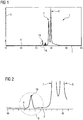
- FIG. 1 an X-ray diffractometer diagram 1 of lead zirconate titanate is shown, which was produced according to a third curve 4 with the method according to the invention.
- a total deposition rate of lead, zirconium and titanium of 15 nm / min was used for the method according to the invention.
- the X-ray diffractometer diagram 1 has an abscissa 2, over which the diffraction angle, and an ordinate 3, over which the amplitude are plotted.
- the thin film was applied to a substrate which is a silicon wafer.
- the third curve 4 has a significant peak value 6 of platinum and a significant peak value 7 of lead-zirconate-titanate in a 111-oriented perovskite structure.
- the substrate was provided with a substrate temperature of 550 ° C.
- the thin film was applied to the substrate by sputtering lead, zirconium and titanium using a lead target, a zirconium target and a titanium target, the total deposition rate of lead, zirconium and titanium being 15 nm / min.
- the deposition rate of lead was chosen such that the atomic concentration of lead based on the atomic concentration of zirconium together with titanium in the thin film is between 1.24 and 1.26.
- the pyroelectric coefficient of the thin film according to the third curve 4 is 2 ⁇ 10 -4 C / m 2 .
- the diffraction angle range 8 between 33 to 35.5 ° is shown in detail in Figure 2 shown.
- a significant peak value is formed at the diffraction angle of 34 to 34.5 °.
- curves 14 and 15 are in Figure 3 has no significant peak value in the diffraction angle range 8 between 33 and 35.5 °.
- the significant peak value 19 at the diffraction angle of 34 to 34.5 ° is only formed in the third curve 4 and not in the first curve 14 and the second curve 15.
Landscapes
- Chemical & Material Sciences (AREA)
- Engineering & Computer Science (AREA)
- Materials Engineering (AREA)
- Chemical Kinetics & Catalysis (AREA)
- Mechanical Engineering (AREA)
- Metallurgy (AREA)
- Organic Chemistry (AREA)
- Manufacturing & Machinery (AREA)
- Ceramic Engineering (AREA)
- Photometry And Measurement Of Optical Pulse Characteristics (AREA)
- Physical Vapour Deposition (AREA)
- Inorganic Compounds Of Heavy Metals (AREA)
- Inorganic Insulating Materials (AREA)
- Crystals, And After-Treatments Of Crystals (AREA)
- Physics & Mathematics (AREA)
- Optics & Photonics (AREA)
Description
- Die Erfindung betrifft ein Verfahren zum Herstellen eines Dünnfilms aus Blei-Zirkonat-Titanat in 111-orientierter Perovskit-Struktur.
- Ein Dünnfilm aus Blei-Zirkonat-Titanat findet in elektronischen Bauteilen Anwendung, wobei die vorteilhaften dielektrischen, pyroelektrischen und piezoelektrischen Eigenschaften des Blei-Zirkonat-Titanats genutzt werden. Derartige elektronische Bauteile sind beispielsweise Kondensatoren, Pyrodetektoren, Piezoaktoren oder Halbleiterspeicher.
- Zur Herstellung des Bauteils wird herkömmlich auf einem Substrat eine erste Elektrodenschicht, darüber der Dünnfilm aus dem Blei-Zirkonat-Titanat und wiederum darüber eine zweite Elektrodenschicht abgeschieden. Der Dünnfilm aus dem Blei-Zirkonat-Titanat wird mit einem Dünnschichtverfahren erzeugt, das bekannterweise ein Sputterverfahren, ein CVD-Verfahren oder ein Sol-Gel-Verfahren ist. Beim Sputterverfahren wird ein Gasgemisch aus Argon und Sauerstoff in einem Vakuum durch eine Hochspannung zu einem Plasma ionisiert. Blei, Zirkon und Titan werden jeweils in Form eines Targets bereitgestellt, wobei die Targets als Kathode und das Substrat als Anode geschaltet sind. Beim Sputtern werden aus den Targets Atome herausgeschlagen, die auf dem Substrat unter Ausbilden des Dünnfilms abgeschieden werden. Das Substrat ist herkömmlich ein Silizium-Wafer, das in nachgelagerten Bearbeitungsschritten membranartig gefertigt wird.
- Für die unterhalb des Dünnfilms auf dem Substrat angeordnete Elektrodenschicht ist als Elektrodenmaterial Platin geeignet, da es die Abscheidebedingungen des Blei-Zirkonat-Titanats bei hohen Substratemperaturen und in sauerstoffhaltiger Atmosphäre beim Sputtern unbeschadet überstehen kann und keine Diffusion in den Dünnfilm auftritt, die zu einer nachteilig veränderten Zusammensetzung und damit zu einer Verschlechterung der Eigenschaften des Dünnfilms führen könnte.
- Die Ausprägung der pyroelektrischen Eigenschaft des Dünnfilms hängt von der Zusammensetzung des Dünnfilm mit Blei, Zirkon und Titan ab. Für die Anwendung des Dünnfilms in einem Infrarotsensor ist der Dünnfilm insbesondere mit einer Dicke von 0,2 bis 3 µm mit dem Sputterverfahren selbstpolarisiert hergestellt. Das Sputterverfahren ist mit einer gesamten Abscheiderate von Blei, Zirkon und Titan zwischen 1 bis 7 nm/min durchzuführen, wobei sich der Dünnfilm mit der 111-orientierten Perovskit-Struktur ausbildet und der Dünnfilm einen pyroelektrischen Koeffizienten zwischen 2·10-9 bis 5·10-4 C/m2 hat.
- Betreffender Stand der Technik wird beispielsweise in folgenden wissenschaftlichen Veröffentlichungen beschrieben:
RAINER BRUCHHAUS ET AL: "Optimized PZT thin films for pyroelectric IR detector arrays",JOURNAL OF ELECTROCERAMICS JUNE 1999, Bd. 3, Nr. 2, 1. Juni 1999 Seiten 151-162. - C. Giebeler ET AL: "High performance PZT based pyro-detectors with D* of 2x10E9 cmHz½/W for presence, gas and spectroscopy applications.",Proceedings OPTO 2009 & IRS2 2009; IRS2 1 - Infrared Sensors, 28. Mai 2009, Seiten 185-189.
- A. A. BOGOMOLOV ET AL: "Photovoltaic and pyroelectric effects in self-polarized ferroelectric PZT(25/75) films",BULLETIN OF THE RUSSIAN ACADEMY OF SCIENCES: PHYSICS, Bd. 74, Nr. 9, 1. September 2010, Seiten 1307-1310.
- G. SUCHANECK ET AL: "Multi-target reactive sputtering-A promising technology for large-area Pb(Zr,Ti)O3 thin film deposition",JOURNAL OF THE EUROPEAN CERAMIC SOCIETY, ELSEVIER SCIENCE PUBLISHERS, BARKING, ESSEX, GB, Bd. 27, Nr. 13-15, 1. Januar 2007, Seiten 3789-3792.
- Nachteilig bei diesem Sputterverfahren ist es, dass die gesamte Abscheiderate von Blei, Zirkon und Titan von 1 bis 7 nm/min lediglich eine geringe Herstellgeschwindigkeit des Dünnfilms darstellt, so dass mit diesem Sputterverfahren lediglich eine geringe Durchsatzrate an Dünnfilmen zu erzielen ist, wodurch die Wirtschaftlichkeit dieses Sputterverfahrens zum Herstellen des Dünnfilms gering ist.
- Im
US Patent 5,196,101 sind Abscheideraten von 10-12 nm/min beschrieben. Der Blei-Zirkonat-Titanat Dünnfilm liegt in 101-Orientierung vor. - Aufgabe der Erfindung ist es, ein Verfahren zum Herstellen eines Dünnfilms aus Blei-Zirkonat-Titanat in 111-orientierter Perovskit-Struktur zu schaffen, wobei mit dem Verfahren eine hohe Durchsatzrate an Dünnfilmen erzielbar ist, obwohl der Dünnfilm einen hohen pyroelektrischen Koeffizienten hat.
- Die Aufgabe wird gelöst mit den Merkmalen des unabhängigen Patentanspruchs 1. Vorteilhafte Ausgestaltungen dazu sind in den weiteren Patentansprüchen angegeben.
- Das Sputtern von Blei, Zirkon und Titan von den jeweiligen Targets auf das Substrat ist bevorzugt konfokal und/oder gleichzeitig. Die Abscheiderate von Blei wird derart gewählt, dass die atomare Konzentration von Blei bezogen auf die atomare Konzentration von Zirkon zusammen mit Titan einen Dünnfilm zwischen 1,1 und 1,3 beträgt. Bei der Substrattemperatur von 500 bis 550°C wird bevorzugtermaßen die gesamte Abscheiderate von Blei, Zirkon und Titan zwischen 11 und 13 nm/min gewählt, wobei bevorzugtermaßen die Abscheiderate von Blei derart gewählt wird, dass die atomare Konzentration von Blei bezogen auf die atomare Konzentration von Zirkon zusammen mit Titan im Dünnfilm zwischen 1,24 und 1,29 beträgt, und bevorzugtermaßen die Abscheiderate von Zirkon derart gewählt wird, dass die atomare Konzentration von Zirkon bezogen auf die atomare Konzentration von Zirkon zusammen mit Titan im Dünnfilm zwischen 0,25 und 0,29 beträgt.
- Der signifikante Spitzenwert des Röntgendiffraktometerdiagramms des Dünnfilms liegt bevorzugt bei dem Beugungswinkel von 34 bis 34,5°. Ferner wird bevorzugt der signifikante Spitzenwert des Röntgendiffraktometerdiagramms des Dünnfilms von Kristallen aus einem Zirkonoxid im Dünnfilm verursacht. Denkbar ist, dass das Zirkonoxid Zirkondioxid oder Zirkontrioxid usw. ist.
- Der Dünnfilm wird bevorzugt so aufgebracht, dass der Dünnfilm selbstpolarisiert ist. In
WO 00/17921 - Der mit dem erfindungsgemäßen Verfahren hergestellte Dünnfilm hat vorteilhaft einen hohen pyroelektrischen Koeffizienten, der etwa zwischen 1,2·10-9 bis 5·10-9 C/m2 liegt, obwohl die gesamte Abscheiderate höher als 10 nm/min beträgt. Dieser vorteilhaft hohe pyroelektrische Koeffizient für den erfindungsgemäß hergestellten Dünnfilm wird bei der hohen gesamten Abscheiderate von mehr als 10 nm/min dadurch erreicht, dass die Abscheiderate von Zirkon derart gewählt wird, dass die atomare Konzentration von Zirkon bezogen auf die atomare Konzentration von Zirkon zusammen mit Titan im Dünnfilm zwischen 0,2 und 0,3 liegt, und die Abscheiderate von Blei in Abhängigkeit der Substrattemperatur und der gesamten Abscheiderate von Blei, Zirkon und Titan so niedrig gewählt wird, dass ein Röntgendiffraktometerdiagramm des 111-orientierten Blei-Zirkonat-Titanats im Bereich des Beugungswinkels von 33 bis 35,5° einen signifikanten Spitzenwert hat.
- Bevorzugt liegt die gesamte Abscheiderate von Blei, Zirkon und Titan zwischen 10 nm/min und 50 nm/min, wobei der erfindungsgemäß hergestellte Dünnfilm in seinem Röntgendiffraktometerdiagramm bevorzugt bei dem Beugungswinkel von 34 bis 34,5° den signifikanten Spitzenwert aufweist. Durch das Auftreten des signifikanten Spitzenwerts im Röntgendiffraktometerdiagramm des erfindungsgemäß hergestellten Blei-Zirkonat-Titanats im Bereich des Beugungswinkels von 33 bis 35,5°, bevorzugt von 34 bis 34,5°, ist eine weitere Phase in dem Dünnfilm erzeugt, die von Kristallen aus einem Zirkonoxid verursacht wird. Das Zirkonoxid kann Zirkondioxid oder Zirkontrioxid oder dergleichen sein.
- Wird hingegen ein Dünnfilm bei einer Substrattemperatur von 550°C hergestellt, wobei die Abscheiderate von Blei so gewählt wird, dass ein Röntgendiffraktometerdiagramm des Blei-Zirkonat-Titanats im Bereich des Beugungswinkels von 33 bis 35,5° keinen signifikanten Spitzenwert hat, so ist der erfindungsgemäß erzielbare hohe pyroelektrische Koeffizient nur dann zu erreichen, wenn die gesamte Abscheiderate von Blei, Zirkon und Titan weniger als 10 nm/min beträgt.
- Dadurch, dass es mit dem erfindungsgemäßen Herstellverfahren ermöglicht ist, die gesamte Abscheiderate von Blei, Zirkon und Titan groß zu wählen, nämlich größer als 10 nm/min, kann mit dem erfindungsgemäßen Verfahren der Dünnfilm schnell und kostengünstig hergestellt werden, obwohl der Dünnfilm dennoch einen hohen pyroelektrischen Koeffizienten hat, nämlich etwa zwischen 1,2·10-9 bis 5·10-4 C/m2.
- Somit ist es vorteilhaft bei der gesamten Abscheiderate von Blei, Zirkon und Titan größer als 10 nm/min den Dünnfilm derart herzustellen, dass das Röntgendiffraktometerdiagramm des Dünnfilms im Bereich des Beugungswinkels von 33 bis 35,5° einen signifikanten Spitzenwert hat, da dadurch der pyroelektrische Koeffizient des Dünnfilms hoch ist.
- Damit das Blei-Zirkonat-Titanat in der Perovskit-Struktur herstellbar ist, ist die Substrattemperatur von über 450°C zu wählen. Die atomare Konzentration von Zirkon bezogen auf die atomare Konzentration von Zirkon zusammen mit Titan im Dünnfilm ist im Wesentlichen unabhängig von der Höhe der Substrattemperatur. Da jedoch Blei eine bezogen auf die Substrattemperatur geringe Verdampfungstemperatur hat, ist das Verhältnis der Abscheiderate von Blei bezogen auf die Abscheiderate von Zirkon zusammen mit Titan entsprechend an die gewählte Substrattemperatur anzupassen, um ein erhöhtes Verdampfen von Blei von dem Substrat bei hohen Substrattemperaturen zu kompensieren. Analog ist bei niedrig gewählter Substrattemperatur die Abscheiderate für Blei entsprechend herabzusenken, da die Verdampfung von Blei reduziert ist. Würde bei der niedrigen Substrattemperatur dennoch die Abscheiderate von Blei zu groß sein, so ist die atomare Konzentration von Blei bezogen auf die atomare Konzentration von Zirkon zusammen mit Titan im Dünnfilm zu hoch, wodurch die 111-Orientierung des Blei-Zirkonat-Titanats nicht erzielbar wäre.
- Um die 111-Orientierung der Perovskit-Struktur des Blei-Zirkonat-Titanats zu erhalten, ist dem abgeschiedenen Blei, Zirkon und Titan mit einer entsprechend hoch gewählten Substrattemperatur eine Aktivierungsenergie bereitzustellen, wodurch das Blei-Zirkonat-Titanat in der 111-orientierten Perovskit-Struktur ausgebildet wird. Es ist bevorzugt beim Sputtern Blei, Zirkon und Titan gleichzeitig auf das Substrat aufzubringen, wodurch sich Blei, Zirkon und Titan zu dem Blei-Zirkonat-Titanat in der 111-orientierten Perovskit-Struktur ausbilden.
- Prinzipiell ist es wünschenswert das Sputtern bei möglichst hohen Abscheideraten von Blei, Zirkon und Titan durchzuführen, da dabei die Durchsatzrate bei der Herstellung des Dünnfilms hoch ist. Jedoch ist bei ungeeignet hoch gewählten Abscheideraten von Blei, Zirkon und Titan nicht mehr genügend Zeit vorhanden, damit sich Blei, Zirkon und Titan in die 111-orientierte Perovskit-Struktur anordnen, da pro Zeiteinheit zu viel Material von den Targets auf das Substrat abgeschieden wird. Um dies zu kompensieren, könnte die Substrattemperatur weiter erhöht werden, wobei mit der Erhöhung der Substrattemperatur eine Erhöhung der Aktivierungsenergie einhergehen müsste, so dass sich die Wahrscheinlichkeit erhöht, dass sich Blei, Zirkon und Titan in der 111-orientierten Perovskit-Struktur anordnen. Im Zuge dessen ist jedoch aufgrund der erhöhten Substrattemperatur die Abscheiderate von Blei zu erhöhen.
- Das hier offenbarte elektronische Bauteil weist als das Substrat eine Membran und den Dünnfilm auf, der auf der Membran aufgebracht ist, wobei der Dünnfilm aus Blei-Zirkonat-Titanat in der 111-orientierten Perovskit-Struktur mit dem erfindungsgemäßen Verfahren hergestellt ist. Das Bauteil wird als eine Wärmebildkamera, ein Präsenzmelder, ein Bewegungsmelder, ein Gasdetektor, ein Gestenerkennungsdetektor, ein Spektroskop und/oder ein Terahertzdetektor verwendet.
- Das Substrat ist bevorzugt ein Silizium-Wafer, auf dem die Membran aus Siliziumdioxid und/oder Siliziumnitrid und/oder Siliziumodioxid aufgebracht ist. Auf der Membran wird eine Elektrode mit einer Haftschicht, beispielsweise aus Aluminiumoxid (Al2O3) oder Titan, gefolgt von einer Platinschicht aufgebracht. Der Dünnfilm wird ganzflächig auf die Platinschicht aufgebracht. In einem nachfolgenden Schritt werden beide Schichten so strukturiert, dass sich ein Pixel oder mehrere Pixel in einem Flächenabschnitt auf der Vorderseite der Membran ausbilden. Das Material des Silizium-Wafers ist auf der dem Dünnfilm abgewandten Seite so abgetragen, dass die Membran zumindest im Bereich des Flächenabschnitts rückseitig freigelegt und thermisch isoliert ist.
- Im Folgenden wird die Erfindung anhand der beigefügten schematischen Zeichnungen erläutert. Es zeigen:
-
Figur 1 ein Röntgendiffraktometerdiagramm von Blei-Zirkonat-Titanat eines erfindungsgemäß hergestellten Dünnfilms; -
Figur 2 einen Ausschnitt des Röntgendiffraktometerdiagramms ausFigur 1 ; und -
Figur 3 ein Röntgendiffraktometerdiagramm von Blei-Zirkonat-Titanat eines herkömmlich hergestellten Dünnfilms. - In
Figur 3 ist ein Röntgendiffraktometerdiagramm 11 von Blei-Zirkonat-Titanat gezeigt, das gemäß einem herkömmlichen Sputterverfahren hergestellt wurde. Das Röntgendiffraktometerdiagramm 11 hat eine Abszisse 12, über die der Beugungswinkel, und eine Ordinate 13, über die die Amplitude aufgetragen sind. Der Dünnfilm wurde auf ein Substrat aufgebracht, wobei das Substrat ein Silikon-Wafer ist. - Eine erste Kurve 14 und eine zweite Kurve 15 zeigen jeweils das Spektrum von Blei-Zirkonat-Titanat eines Dünnfilms. Die Dünnfilme wurden mit dem herkömmlichen Sputterverfahren auf das Substrat aufgebracht, wobei gemäß der ersten Kurve 14 die Substrattemperatur 500°C und gemäß der zweiten Kurve 15 die Substrattemperatur 550°C betragen hat. Beide Dünnfilme wurden bei einer gesamten Abscheiderate von Blei, Zirkon und Titan von 5 nm/min hergestellt, wobei der pyroelektrische Koeffizient etwa 2·10-4 C/m2 beträgt.
- In beiden Kurven 14 und 15 ist ein signifikanter Spitzenwert 16 von Platin und ein signifikanter Spitzenwert 17 von Blei-Zirkonat-Titanat in 111-orientierter Perovskit-Struktur zu erkennen. Der leicht unruhige Verlauf der Kurven 14 und 15 ist auf Grundrauschen zurückzuführen. Im Beugungswinkelbereich 18 von 33 bis 35,5° tritt ein signifikanter Spitzenwert nicht auf.
- In
Figur 1 ist ein Röntgendiffraktometerdiagramm 1 von Blei-Zirkonat-Titanat gezeigt, das gemäß einer dritten Kurve 4 mit dem erfindungsgemäßen Verfahren hergestellt wurde. Für das erfindungsgemäße Verfahren wurde eine gesamte Abscheiderate von Blei, Zirkon und Titan von 15 nm/min verwendet. Das Röntgendiffraktometerdiagramm 1 weist eine Abszisse 2, über die der Beugungswinkel, und eine Ordinate 3 auf, über die die Amplitude aufgetragen sind. Der Dünnfilm wurde auf ein Substrat aufgebracht, das ein Silikon-Wafer ist. - Die dritte Kurve 4 weiset einen signifikanten Spitzenwert 6 von Platin und einen signifikanten Spitzenwert 7 von Blei-Zirkonat-Titanat in 111-orientierter Perovskit-Struktur auf. Beim Herstellen des Dünnfilms wurde das Substrat mit einer Substrattemperatur 550°C bereitgestellt. Der Dünnfilm wurde durch Sputtern von Blei, Zirkon und Titan unter Verwendung eines Blei-Targets, eines Zirkon-Targets und eines Titan-Targets auf das Substrat aufgebracht, wobei die gesamte Abscheiderate von Blei, Zirkon und Titan 15 nm/min betrug.
- Für den Dünnfilm gemäß der dritten Kurve 4 wurde die Abscheiderate von Blei derart gewählt, dass die atomare Konzentration von Blei bezogen auf die atomare Konzentration von Zirkon zusammen mit Titan im Dünnfilm zwischen 1,24 und 1,26 beträgt. Der pyroelektrische Koeffizient des Dünnfilms gemäß der dritten Kurve 4 beträgt 2·10-4 C/m2.
- Der Beugungswinkelbereich 8 zwischen 33 bis 35,5° ist im Detail in
Figur 2 gezeigt. In der dritten Kurve 4 ist ein signifikanter Spitzenwert bei dem Beugungswinkel von 34 bis 34,5° ausgebildet. Im Gegensatz dazu haben die Kurven 14 und 15 inFigur 3 im Beugungswinkelbereich 8 zwischen 33 bis 35,5° keinen signifikanten Spitzenwert hat. Der signifikante Spitzenwert 19 bei dem Beugungswinkel von 34 bis 34,5° ist lediglich in der dritten Kurve 4 und nicht in der ersten Kurve 14 und der zweiten Kurve 15 ausgebildet. -
- 1 Röntgendiffraktometerdiagramm
(gesamte Abscheiderate bei 15 nm/min) - 2 Abszisse: Beugungswinkel
- 3 Ordinate: Amlitude
- 4 dritte Kurve
- 6 signifikanter Spitzenwert von Blei
- 7 signifikanter Spitzenwert von Blei-Zirkonat-Titanat
- 8 Beugungswinkelbereich von 33 bis 35,5°
- 9 signifikanter Spitzenwert bei dem Beugungswinkel von 34 bis 34,5°
- 11 Röntgendiffraktometerdiagramm
(gesamte Abscheiderate bei 5 nm/min) - 12 Abszisse: Beugungswinkel
- 13 Ordinate: Amlitude
- 14 erste Kurve (Substrattemperatur bei 450°C)
- 15 zweite Kurve (Substrattemperatur bei 550°C)
- 16 Signifikanter Spitzenwert von Blei
- 17 Signifikanter Spitzenwert von Blei-Zirkonat-Titanat
- 18 Beugungswinkelbereich von 33 bis 35,5°
Claims (8)
- Verfahren zum Herstellen eines Dünnfilms aus Blei-Zirkonat-Titanat in 111-orientierter Perowskit-Struktur, mit den Schritten:- Bereitstellen eines Substrats mit einer Substrattemperatur von 500 bis 550°C und eines Blei-Targets, eines Zirkon-Targets und eines Titan-Targets;- Aufbringen des Dünnfilms durch Sputtern von Blei, Zirkon und Titan von den jeweiligen Targets auf das Substrat, wobei-- die gesamte Abscheiderate von Blei, Zirkon und Titan größer als 10 nm/min ist,-- die Abscheiderate von Zirkon derart gewählt wird, dass die atomare Konzentration von Zirkon bezogen auf die atomare Konzentration von Zirkon zusammen mit Titan im Dünnfilm zwischen 0,2 und 0,3 liegt, und-- die Abscheiderate von Blei in Abhängigkeit der Substrattemperatur und der gesamten Abscheiderate von Blei, Zirkon und Titan so niedrig gewählt wird, dass ein Röntgendiffraktometerdiagramm des 111-orientierten Blei-Zirkonat-Titanats im Bereich des Beugungswinkels von 33 bis 35,5° einen signifikanten Spitzenwert (19) hat;-- die Abscheiderate von Blei derart gewählt wird, dass die atomare Konzentration von Blei bezogen auf die atomare Konzentration von Zirkon zusammen mit Titan im Dünnfilm zwischen 1,1 und 1,3 beträgt; und- Fertigstellen des Dünnfilms.
- Verfahren gemäß Anspruch 1, wobei das Sputtern von Blei, Zirkon und Titan von den jeweiligen Targets auf das Substrat konfokal und/oder gleichzeitig ist.
- Verfahren gemäß Ansprüche 1 oder 2, wobei bei der Substrattemperatur von 500 bis 550 °C die gesamte Abscheiderate von Blei, Zirkon und Titan zwischen 11 und 13 nm/min gewählt wird, die Abscheiderate von Blei derart gewählt wird, dass die atomare Konzentration von Blei bezogen auf die atomare Konzentration von Zirkon zusammen mit Titan im Dünnfilm zwischen 1,24 und 1,29 beträgt, und die Abscheiderate von Zirkon derart gewählt wird, dass die atomare Konzentration von Zirkon bezogen auf die atomare Konzentration von Zirkon zusammen mit Titan im Dünnfilm zwischen 0,25 und 0,29 beträgt.
- Verfahren gemäß einem der Ansprüche 1 bis 3, wobei der signifikante Spitzenwert des Röntgendiffraktometerdiagramms des Dünnfilms bei dem Beugungswinkel von 34 bis 34,5° liegt.
- Verfahren gemäß einem der Ansprüche 1 bis 3, wobei der signifikante Spitzenwert des Röntgendiffraktometerdiagramms des Dünnfilms von Kristallen aus einem Zirkonoxid im Dünnfilm verursacht wird.
- Verfahren gemäß einem der Ansprüche 1 bis 5, wobei der Dünnfilm so aufgebracht wird, dass der Dünnfilm selbstpolarisiert ist.
- Verfahren gemäß einem der Ansprüche 1 bis 6, mit dem Schritt: Polarisieren des Dünnfilms derart, dass der pyroelektrische Koeffizient des Dünnfilms größer als 10-4 C/m2 ist.
- Verfahren gemäß einem der Ansprüche 1 bis 7, wobei der Dünnfilm eine Dicke zwischen 0,2 bis 3 µm hat.
Applications Claiming Priority (2)
| Application Number | Priority Date | Filing Date | Title |
|---|---|---|---|
| DE102011000752A DE102011000752B3 (de) | 2011-02-15 | 2011-02-15 | Verfahren zum Herstellen eines Dünnfilms aus Blei-Zirkonat-Titanat, elektronisches Bauteil mit dem Dünnfilm und Verwendung des Bauteils |
| PCT/EP2012/052419 WO2012110458A1 (de) | 2011-02-15 | 2012-02-13 | Verfahren zum herstellen eines dünnfilms aus blei-zirkonat-titanat |
Publications (2)
| Publication Number | Publication Date |
|---|---|
| EP2675935A1 EP2675935A1 (de) | 2013-12-25 |
| EP2675935B1 true EP2675935B1 (de) | 2021-04-07 |
Family
ID=45755319
Family Applications (1)
| Application Number | Title | Priority Date | Filing Date |
|---|---|---|---|
| EP12705252.0A Active EP2675935B1 (de) | 2011-02-15 | 2012-02-13 | Verfahren zum herstellen eines dünnfilms aus blei-zirkonat-titanat |
Country Status (5)
| Country | Link |
|---|---|
| US (1) | US9960344B2 (de) |
| EP (1) | EP2675935B1 (de) |
| CN (1) | CN103547700B (de) |
| DE (1) | DE102011000752B3 (de) |
| WO (1) | WO2012110458A1 (de) |
Families Citing this family (8)
| Publication number | Priority date | Publication date | Assignee | Title |
|---|---|---|---|---|
| DE102012105036A1 (de) * | 2012-06-12 | 2013-12-12 | Pyreos Ltd. | Verfahren zum Herstellen eines Mikrosystems |
| DE102012107739B4 (de) * | 2012-08-22 | 2023-11-02 | Avago Technologies International Sales Pte. Ltd. | Sensorsystem zum Erkennen einer Bewegung einer Infrarotlichtquelle |
| JP2014235144A (ja) * | 2013-06-05 | 2014-12-15 | セイコーエプソン株式会社 | テラヘルツ波検出装置、カメラ、イメージング装置および計測装置 |
| DE102018004257B4 (de) * | 2017-08-28 | 2023-07-27 | Spectrolytic Ltd. | Mikromechanikstruktur und Verfahren zum Herstellen der Mikromechanikstruktur |
| CN108559954B (zh) * | 2018-03-30 | 2020-01-21 | 湖北大学 | 一种负热膨胀锆钛酸铅薄膜的制备方法 |
| CN108493768A (zh) * | 2018-04-10 | 2018-09-04 | 中国科学院半导体研究所 | 脊型波导结构激光器p型电极的制备方法 |
| CN113249789B (zh) * | 2021-05-17 | 2022-05-10 | 浙江大学 | 一种单晶锆钛酸铅薄膜及其制备和应用 |
| CN116103608A (zh) * | 2023-01-12 | 2023-05-12 | 深圳通感微电子有限公司 | Pzt陶瓷薄膜及其制备方法 |
Family Cites Families (4)
| Publication number | Priority date | Publication date | Assignee | Title |
|---|---|---|---|---|
| US5196101A (en) * | 1991-02-05 | 1993-03-23 | Califoria Institute Of Technology | Deposition of thin films of multicomponent materials |
| JP2877618B2 (ja) * | 1992-07-06 | 1999-03-31 | シャープ株式会社 | 強誘電体膜の形成方法 |
| EP0600303B1 (de) * | 1992-12-01 | 2002-02-06 | Matsushita Electric Industrial Co., Ltd. | Verfahren zur Herstellung einer elektrischen Dünnschicht |
| DE19842816C1 (de) | 1998-09-18 | 2000-02-03 | Siemens Ag | Verfahren zur Herstellung selbstpolarisierter ferroelektrischer Schichten, insbesondere PZT-Schichten, mit rhomboedrischer Kristallstruktur |
-
2011
- 2011-02-15 DE DE102011000752A patent/DE102011000752B3/de active Active
-
2012
- 2012-02-13 EP EP12705252.0A patent/EP2675935B1/de active Active
- 2012-02-13 WO PCT/EP2012/052419 patent/WO2012110458A1/de not_active Ceased
- 2012-02-13 CN CN201280018356.7A patent/CN103547700B/zh active Active
- 2012-02-13 US US13/985,646 patent/US9960344B2/en active Active
Non-Patent Citations (1)
| Title |
|---|
| SCHREITER M ET AL: "Sputtering of self-polarized PZT films for IR-detector arrays", APPLICATIONS OF FERROELECTRICS, 1998. ISAF 98. PROCEEDINGS OF THE ELEVENTH IEEE INTERNATIONAL SYMPOSIUM ON MONTREUX, SWITZERLAND 24-27 AUG. 1998, PISCATAWAY, NJ, USA,IEEE, US, 24 August 1998 (1998-08-24), pages 181 - 185, XP010347216, ISBN: 978-0-7803-4959-9, DOI: 10.1109/ISAF.1998.786665 * |
Also Published As
| Publication number | Publication date |
|---|---|
| DE102011000752B3 (de) | 2012-06-06 |
| US20140049136A1 (en) | 2014-02-20 |
| EP2675935A1 (de) | 2013-12-25 |
| CN103547700B (zh) | 2015-09-30 |
| WO2012110458A1 (de) | 2012-08-23 |
| US9960344B2 (en) | 2018-05-01 |
| CN103547700A (zh) | 2014-01-29 |
Similar Documents
| Publication | Publication Date | Title |
|---|---|---|
| DE102011000752B3 (de) | Verfahren zum Herstellen eines Dünnfilms aus Blei-Zirkonat-Titanat, elektronisches Bauteil mit dem Dünnfilm und Verwendung des Bauteils | |
| DE69735011T2 (de) | Verfahren zur Herstellung einer piezoelektrischen Dünnschichtanordnung | |
| EP2412040B1 (de) | Dünnschichtverkapselung für ein optoelektronisches bauelement, verfahren zu dessen herstellung und optoelektronisches bauelement | |
| DE69617288T2 (de) | Verfahren zur Herstellung einer piezoelektrischen Dünnschicht | |
| EP3011370B1 (de) | Verfahren zur herstellung einer entspiegelungsschicht | |
| US20120295099A1 (en) | Method for producing ferroelectric thin film | |
| WO2009127373A1 (de) | Transparentes barriereschichtsystem | |
| DE102017106405A1 (de) | Piezoelektrisches keramisches sputtertarget, bleifreier piezoelektrischer dünnfilm und piezoelektrisches dünnfilmelement unter verwendung der selbigen | |
| DE102016100907B4 (de) | Verfahren zur Herstellung eines reflexionsmindernden Schichtsystems | |
| Özden et al. | Structural and Surface Characterization of PZT (52/48) Films Deposited by Spin Coating Method | |
| EP0676384A2 (de) | Perowskithaltiger Verbundwerkstoff, Verfahren zu seiner Herstellung, elektronisches Bauelement und Modul | |
| EP3587617B1 (de) | Verfahren zum herstellen eines mikrosystems mit einer dünnschicht aus bleizirkonattitanat | |
| WO2007134914A1 (de) | Szintillatorplatte | |
| DE102011017403A1 (de) | Verfahren zum Abscheiden eines transparenten Barriereschichtsystems | |
| EP2468915B1 (de) | Verfahren zum Abscheiden dielektrischer Schichten im Vakuum sowie Verwendung des Verfahrens | |
| DE102018004257B4 (de) | Mikromechanikstruktur und Verfahren zum Herstellen der Mikromechanikstruktur | |
| EP2699705B1 (de) | Verfahren zum abscheiden eines transparenten barriereschichtsystems | |
| EP2644740A2 (de) | Verfahren zum Herstellen einer Dünnschicht auf einem Substrat | |
| WO2009083181A1 (de) | Vorrichtung zur detektion von wärmestrahlung mit einem pyroelektrischen detektor-array, verfahren zum herstellen und verwendung der vorrichtung | |
| DE102020200237B4 (de) | Verfahren zur Herstellung eines piezoelektrischen Mehrschicht-Sensors und/oder Aktuators | |
| DE102016002597A1 (de) | Breitbandentspiegelung für den NlR-Bereich | |
| DE112024001148T5 (de) | Verbundsubstrat und Verfahren zur Herstellung eines Verbundsubstrats | |
| DE102024127647A1 (de) | Piezoelektrisches element und aktuator | |
| DE112017003091B4 (de) | Piezoelektrischer Film, Piezoelektrisches Element und Verfahren zur Herstellung eines Piezoelektrischen Films | |
| DE102017104161A1 (de) | Verfahren zur Herstellung einer reflexionsmindernden Beschichtung |
Legal Events
| Date | Code | Title | Description |
|---|---|---|---|
| PUAI | Public reference made under article 153(3) epc to a published international application that has entered the european phase |
Free format text: ORIGINAL CODE: 0009012 |
|
| 17P | Request for examination filed |
Effective date: 20130816 |
|
| AK | Designated contracting states |
Kind code of ref document: A1 Designated state(s): AL AT BE BG CH CY CZ DE DK EE ES FI FR GB GR HR HU IE IS IT LI LT LU LV MC MK MT NL NO PL PT RO RS SE SI SK SM TR |
|
| DAX | Request for extension of the european patent (deleted) | ||
| 17Q | First examination report despatched |
Effective date: 20150708 |
|
| GRAP | Despatch of communication of intention to grant a patent |
Free format text: ORIGINAL CODE: EPIDOSNIGR1 |
|
| STAA | Information on the status of an ep patent application or granted ep patent |
Free format text: STATUS: GRANT OF PATENT IS INTENDED |
|
| RIC1 | Information provided on ipc code assigned before grant |
Ipc: H01L 37/02 20060101ALI20200708BHEP Ipc: H01L 21/02 20060101ALI20200708BHEP Ipc: H01L 41/316 20130101ALI20200708BHEP Ipc: C23C 14/34 20060101ALI20200708BHEP Ipc: C23C 14/08 20060101AFI20200708BHEP |
|
| INTG | Intention to grant announced |
Effective date: 20200727 |
|
| GRAS | Grant fee paid |
Free format text: ORIGINAL CODE: EPIDOSNIGR3 |
|
| GRAA | (expected) grant |
Free format text: ORIGINAL CODE: 0009210 |
|
| STAA | Information on the status of an ep patent application or granted ep patent |
Free format text: STATUS: THE PATENT HAS BEEN GRANTED |
|
| RBV | Designated contracting states (corrected) |
Designated state(s): AL AT BE BG CH CY CZ DK EE ES FI FR GB GR HR HU IE IS IT LI LT LU LV MC MK MT NL NO PL PT RO RS SE SI SK SM TR |
|
| REG | Reference to a national code |
Ref country code: DE Ref legal event code: R108 |
|
| AK | Designated contracting states |
Kind code of ref document: B1 Designated state(s): AL AT BE BG CH CY CZ DK EE ES FI FR GB GR HR HU IE IS IT LI LT LU LV MC MK MT NL NO PL PT RO RS SE SI SK SM TR |
|
| REG | Reference to a national code |
Ref country code: GB Ref legal event code: FG4D Free format text: NOT ENGLISH |
|
| REG | Reference to a national code |
Ref country code: AT Ref legal event code: REF Ref document number: 1379788 Country of ref document: AT Kind code of ref document: T Effective date: 20210415 Ref country code: CH Ref legal event code: EP |
|
| REG | Reference to a national code |
Ref country code: IE Ref legal event code: FG4D Free format text: LANGUAGE OF EP DOCUMENT: GERMAN |
|
| REG | Reference to a national code |
Ref country code: LT Ref legal event code: MG9D |
|
| REG | Reference to a national code |
Ref country code: NL Ref legal event code: MP Effective date: 20210407 |
|
| PG25 | Lapsed in a contracting state [announced via postgrant information from national office to epo] |
Ref country code: HR Free format text: LAPSE BECAUSE OF FAILURE TO SUBMIT A TRANSLATION OF THE DESCRIPTION OR TO PAY THE FEE WITHIN THE PRESCRIBED TIME-LIMIT Effective date: 20210407 Ref country code: BG Free format text: LAPSE BECAUSE OF FAILURE TO SUBMIT A TRANSLATION OF THE DESCRIPTION OR TO PAY THE FEE WITHIN THE PRESCRIBED TIME-LIMIT Effective date: 20210707 Ref country code: FI Free format text: LAPSE BECAUSE OF FAILURE TO SUBMIT A TRANSLATION OF THE DESCRIPTION OR TO PAY THE FEE WITHIN THE PRESCRIBED TIME-LIMIT Effective date: 20210407 Ref country code: NL Free format text: LAPSE BECAUSE OF FAILURE TO SUBMIT A TRANSLATION OF THE DESCRIPTION OR TO PAY THE FEE WITHIN THE PRESCRIBED TIME-LIMIT Effective date: 20210407 Ref country code: LT Free format text: LAPSE BECAUSE OF FAILURE TO SUBMIT A TRANSLATION OF THE DESCRIPTION OR TO PAY THE FEE WITHIN THE PRESCRIBED TIME-LIMIT Effective date: 20210407 |
|
| PG25 | Lapsed in a contracting state [announced via postgrant information from national office to epo] |
Ref country code: SE Free format text: LAPSE BECAUSE OF FAILURE TO SUBMIT A TRANSLATION OF THE DESCRIPTION OR TO PAY THE FEE WITHIN THE PRESCRIBED TIME-LIMIT Effective date: 20210407 Ref country code: RS Free format text: LAPSE BECAUSE OF FAILURE TO SUBMIT A TRANSLATION OF THE DESCRIPTION OR TO PAY THE FEE WITHIN THE PRESCRIBED TIME-LIMIT Effective date: 20210407 Ref country code: GR Free format text: LAPSE BECAUSE OF FAILURE TO SUBMIT A TRANSLATION OF THE DESCRIPTION OR TO PAY THE FEE WITHIN THE PRESCRIBED TIME-LIMIT Effective date: 20210708 Ref country code: LV Free format text: LAPSE BECAUSE OF FAILURE TO SUBMIT A TRANSLATION OF THE DESCRIPTION OR TO PAY THE FEE WITHIN THE PRESCRIBED TIME-LIMIT Effective date: 20210407 Ref country code: IS Free format text: LAPSE BECAUSE OF FAILURE TO SUBMIT A TRANSLATION OF THE DESCRIPTION OR TO PAY THE FEE WITHIN THE PRESCRIBED TIME-LIMIT Effective date: 20210807 Ref country code: NO Free format text: LAPSE BECAUSE OF FAILURE TO SUBMIT A TRANSLATION OF THE DESCRIPTION OR TO PAY THE FEE WITHIN THE PRESCRIBED TIME-LIMIT Effective date: 20210707 Ref country code: PL Free format text: LAPSE BECAUSE OF FAILURE TO SUBMIT A TRANSLATION OF THE DESCRIPTION OR TO PAY THE FEE WITHIN THE PRESCRIBED TIME-LIMIT Effective date: 20210407 Ref country code: PT Free format text: LAPSE BECAUSE OF FAILURE TO SUBMIT A TRANSLATION OF THE DESCRIPTION OR TO PAY THE FEE WITHIN THE PRESCRIBED TIME-LIMIT Effective date: 20210809 Ref country code: ES Free format text: LAPSE BECAUSE OF FAILURE TO SUBMIT A TRANSLATION OF THE DESCRIPTION OR TO PAY THE FEE WITHIN THE PRESCRIBED TIME-LIMIT Effective date: 20210407 |
|
| PG25 | Lapsed in a contracting state [announced via postgrant information from national office to epo] |
Ref country code: RO Free format text: LAPSE BECAUSE OF FAILURE TO SUBMIT A TRANSLATION OF THE DESCRIPTION OR TO PAY THE FEE WITHIN THE PRESCRIBED TIME-LIMIT Effective date: 20210407 Ref country code: SM Free format text: LAPSE BECAUSE OF FAILURE TO SUBMIT A TRANSLATION OF THE DESCRIPTION OR TO PAY THE FEE WITHIN THE PRESCRIBED TIME-LIMIT Effective date: 20210407 Ref country code: SK Free format text: LAPSE BECAUSE OF FAILURE TO SUBMIT A TRANSLATION OF THE DESCRIPTION OR TO PAY THE FEE WITHIN THE PRESCRIBED TIME-LIMIT Effective date: 20210407 Ref country code: CZ Free format text: LAPSE BECAUSE OF FAILURE TO SUBMIT A TRANSLATION OF THE DESCRIPTION OR TO PAY THE FEE WITHIN THE PRESCRIBED TIME-LIMIT Effective date: 20210407 Ref country code: DK Free format text: LAPSE BECAUSE OF FAILURE TO SUBMIT A TRANSLATION OF THE DESCRIPTION OR TO PAY THE FEE WITHIN THE PRESCRIBED TIME-LIMIT Effective date: 20210407 Ref country code: EE Free format text: LAPSE BECAUSE OF FAILURE TO SUBMIT A TRANSLATION OF THE DESCRIPTION OR TO PAY THE FEE WITHIN THE PRESCRIBED TIME-LIMIT Effective date: 20210407 |
|
| PLBE | No opposition filed within time limit |
Free format text: ORIGINAL CODE: 0009261 |
|
| STAA | Information on the status of an ep patent application or granted ep patent |
Free format text: STATUS: NO OPPOSITION FILED WITHIN TIME LIMIT |
|
| 26N | No opposition filed |
Effective date: 20220110 |
|
| PG25 | Lapsed in a contracting state [announced via postgrant information from national office to epo] |
Ref country code: IS Free format text: LAPSE BECAUSE OF FAILURE TO SUBMIT A TRANSLATION OF THE DESCRIPTION OR TO PAY THE FEE WITHIN THE PRESCRIBED TIME-LIMIT Effective date: 20210807 Ref country code: AL Free format text: LAPSE BECAUSE OF FAILURE TO SUBMIT A TRANSLATION OF THE DESCRIPTION OR TO PAY THE FEE WITHIN THE PRESCRIBED TIME-LIMIT Effective date: 20210407 |
|
| PG25 | Lapsed in a contracting state [announced via postgrant information from national office to epo] |
Ref country code: IT Free format text: LAPSE BECAUSE OF FAILURE TO SUBMIT A TRANSLATION OF THE DESCRIPTION OR TO PAY THE FEE WITHIN THE PRESCRIBED TIME-LIMIT Effective date: 20210407 |
|
| PG25 | Lapsed in a contracting state [announced via postgrant information from national office to epo] |
Ref country code: MC Free format text: LAPSE BECAUSE OF FAILURE TO SUBMIT A TRANSLATION OF THE DESCRIPTION OR TO PAY THE FEE WITHIN THE PRESCRIBED TIME-LIMIT Effective date: 20210407 |
|
| REG | Reference to a national code |
Ref country code: BE Ref legal event code: MM Effective date: 20220228 |
|
| PG25 | Lapsed in a contracting state [announced via postgrant information from national office to epo] |
Ref country code: LU Free format text: LAPSE BECAUSE OF NON-PAYMENT OF DUE FEES Effective date: 20220213 |
|
| PG25 | Lapsed in a contracting state [announced via postgrant information from national office to epo] |
Ref country code: IE Free format text: LAPSE BECAUSE OF NON-PAYMENT OF DUE FEES Effective date: 20220213 |
|
| PG25 | Lapsed in a contracting state [announced via postgrant information from national office to epo] |
Ref country code: BE Free format text: LAPSE BECAUSE OF NON-PAYMENT OF DUE FEES Effective date: 20220228 |
|
| REG | Reference to a national code |
Ref country code: AT Ref legal event code: MM01 Ref document number: 1379788 Country of ref document: AT Kind code of ref document: T Effective date: 20220213 |
|
| PG25 | Lapsed in a contracting state [announced via postgrant information from national office to epo] |
Ref country code: AT Free format text: LAPSE BECAUSE OF NON-PAYMENT OF DUE FEES Effective date: 20220213 |
|
| PG25 | Lapsed in a contracting state [announced via postgrant information from national office to epo] |
Ref country code: HU Free format text: LAPSE BECAUSE OF FAILURE TO SUBMIT A TRANSLATION OF THE DESCRIPTION OR TO PAY THE FEE WITHIN THE PRESCRIBED TIME-LIMIT; INVALID AB INITIO Effective date: 20120213 |
|
| PG25 | Lapsed in a contracting state [announced via postgrant information from national office to epo] |
Ref country code: MK Free format text: LAPSE BECAUSE OF FAILURE TO SUBMIT A TRANSLATION OF THE DESCRIPTION OR TO PAY THE FEE WITHIN THE PRESCRIBED TIME-LIMIT Effective date: 20210407 Ref country code: CY Free format text: LAPSE BECAUSE OF FAILURE TO SUBMIT A TRANSLATION OF THE DESCRIPTION OR TO PAY THE FEE WITHIN THE PRESCRIBED TIME-LIMIT Effective date: 20210407 |
|
| PG25 | Lapsed in a contracting state [announced via postgrant information from national office to epo] |
Ref country code: TR Free format text: LAPSE BECAUSE OF FAILURE TO SUBMIT A TRANSLATION OF THE DESCRIPTION OR TO PAY THE FEE WITHIN THE PRESCRIBED TIME-LIMIT Effective date: 20210407 |
|
| PG25 | Lapsed in a contracting state [announced via postgrant information from national office to epo] |
Ref country code: MT Free format text: LAPSE BECAUSE OF FAILURE TO SUBMIT A TRANSLATION OF THE DESCRIPTION OR TO PAY THE FEE WITHIN THE PRESCRIBED TIME-LIMIT Effective date: 20210407 |
|
| REG | Reference to a national code |
Ref country code: CH Ref legal event code: U11 Free format text: ST27 STATUS EVENT CODE: U-0-0-U10-U11 (AS PROVIDED BY THE NATIONAL OFFICE) Effective date: 20260301 |
|
| PGFP | Annual fee paid to national office [announced via postgrant information from national office to epo] |
Ref country code: GB Payment date: 20260121 Year of fee payment: 15 |
|
| PGFP | Annual fee paid to national office [announced via postgrant information from national office to epo] |
Ref country code: FR Payment date: 20260121 Year of fee payment: 15 |
|
| PGFP | Annual fee paid to national office [announced via postgrant information from national office to epo] |
Ref country code: CH Payment date: 20260301 Year of fee payment: 15 |