EP2671965A2 - Verfahren zur Herstellung einer dünnschichtigen Polysiliziumschicht und Verfahren zur Bildung eines Dünnschichttransistors - Google Patents
Verfahren zur Herstellung einer dünnschichtigen Polysiliziumschicht und Verfahren zur Bildung eines Dünnschichttransistors Download PDFInfo
- Publication number
- EP2671965A2 EP2671965A2 EP13171120.2A EP13171120A EP2671965A2 EP 2671965 A2 EP2671965 A2 EP 2671965A2 EP 13171120 A EP13171120 A EP 13171120A EP 2671965 A2 EP2671965 A2 EP 2671965A2
- Authority
- EP
- European Patent Office
- Prior art keywords
- thin film
- heating
- layer
- substrate
- forming
- Prior art date
- Legal status (The legal status is an assumption and is not a legal conclusion. Google has not performed a legal analysis and makes no representation as to the accuracy of the status listed.)
- Withdrawn
Links
Images










Classifications
-
- C—CHEMISTRY; METALLURGY
- C23—COATING METALLIC MATERIAL; COATING MATERIAL WITH METALLIC MATERIAL; CHEMICAL SURFACE TREATMENT; DIFFUSION TREATMENT OF METALLIC MATERIAL; COATING BY VACUUM EVAPORATION, BY SPUTTERING, BY ION IMPLANTATION OR BY CHEMICAL VAPOUR DEPOSITION, IN GENERAL; INHIBITING CORROSION OF METALLIC MATERIAL OR INCRUSTATION IN GENERAL
- C23C—COATING METALLIC MATERIAL; COATING MATERIAL WITH METALLIC MATERIAL; SURFACE TREATMENT OF METALLIC MATERIAL BY DIFFUSION INTO THE SURFACE, BY CHEMICAL CONVERSION OR SUBSTITUTION; COATING BY VACUUM EVAPORATION, BY SPUTTERING, BY ION IMPLANTATION OR BY CHEMICAL VAPOUR DEPOSITION, IN GENERAL
- C23C14/00—Coating by vacuum evaporation, by sputtering or by ion implantation of the coating forming material
- C23C14/02—Pretreatment of the material to be coated
- C23C14/024—Deposition of sublayers, e.g. to promote adhesion of the coating
-
- C—CHEMISTRY; METALLURGY
- C23—COATING METALLIC MATERIAL; COATING MATERIAL WITH METALLIC MATERIAL; CHEMICAL SURFACE TREATMENT; DIFFUSION TREATMENT OF METALLIC MATERIAL; COATING BY VACUUM EVAPORATION, BY SPUTTERING, BY ION IMPLANTATION OR BY CHEMICAL VAPOUR DEPOSITION, IN GENERAL; INHIBITING CORROSION OF METALLIC MATERIAL OR INCRUSTATION IN GENERAL
- C23C—COATING METALLIC MATERIAL; COATING MATERIAL WITH METALLIC MATERIAL; SURFACE TREATMENT OF METALLIC MATERIAL BY DIFFUSION INTO THE SURFACE, BY CHEMICAL CONVERSION OR SUBSTITUTION; COATING BY VACUUM EVAPORATION, BY SPUTTERING, BY ION IMPLANTATION OR BY CHEMICAL VAPOUR DEPOSITION, IN GENERAL
- C23C14/00—Coating by vacuum evaporation, by sputtering or by ion implantation of the coating forming material
- C23C14/02—Pretreatment of the material to be coated
- C23C14/024—Deposition of sublayers, e.g. to promote adhesion of the coating
- C23C14/025—Metallic sublayers
-
- C—CHEMISTRY; METALLURGY
- C23—COATING METALLIC MATERIAL; COATING MATERIAL WITH METALLIC MATERIAL; CHEMICAL SURFACE TREATMENT; DIFFUSION TREATMENT OF METALLIC MATERIAL; COATING BY VACUUM EVAPORATION, BY SPUTTERING, BY ION IMPLANTATION OR BY CHEMICAL VAPOUR DEPOSITION, IN GENERAL; INHIBITING CORROSION OF METALLIC MATERIAL OR INCRUSTATION IN GENERAL
- C23C—COATING METALLIC MATERIAL; COATING MATERIAL WITH METALLIC MATERIAL; SURFACE TREATMENT OF METALLIC MATERIAL BY DIFFUSION INTO THE SURFACE, BY CHEMICAL CONVERSION OR SUBSTITUTION; COATING BY VACUUM EVAPORATION, BY SPUTTERING, BY ION IMPLANTATION OR BY CHEMICAL VAPOUR DEPOSITION, IN GENERAL
- C23C14/00—Coating by vacuum evaporation, by sputtering or by ion implantation of the coating forming material
- C23C14/06—Coating by vacuum evaporation, by sputtering or by ion implantation of the coating forming material characterised by the coating material
- C23C14/14—Metallic material, boron or silicon
- C23C14/18—Metallic material, boron or silicon on other inorganic substrates
- C23C14/185—Metallic material, boron or silicon on other inorganic substrates by cathodic sputtering
-
- C—CHEMISTRY; METALLURGY
- C23—COATING METALLIC MATERIAL; COATING MATERIAL WITH METALLIC MATERIAL; CHEMICAL SURFACE TREATMENT; DIFFUSION TREATMENT OF METALLIC MATERIAL; COATING BY VACUUM EVAPORATION, BY SPUTTERING, BY ION IMPLANTATION OR BY CHEMICAL VAPOUR DEPOSITION, IN GENERAL; INHIBITING CORROSION OF METALLIC MATERIAL OR INCRUSTATION IN GENERAL
- C23C—COATING METALLIC MATERIAL; COATING MATERIAL WITH METALLIC MATERIAL; SURFACE TREATMENT OF METALLIC MATERIAL BY DIFFUSION INTO THE SURFACE, BY CHEMICAL CONVERSION OR SUBSTITUTION; COATING BY VACUUM EVAPORATION, BY SPUTTERING, BY ION IMPLANTATION OR BY CHEMICAL VAPOUR DEPOSITION, IN GENERAL
- C23C16/00—Chemical coating by decomposition of gaseous compounds, without leaving reaction products of surface material in the coating, i.e. chemical vapour deposition [CVD] processes
- C23C16/02—Pretreatment of the material to be coated
- C23C16/0209—Pretreatment of the material to be coated by heating
-
- C—CHEMISTRY; METALLURGY
- C23—COATING METALLIC MATERIAL; COATING MATERIAL WITH METALLIC MATERIAL; CHEMICAL SURFACE TREATMENT; DIFFUSION TREATMENT OF METALLIC MATERIAL; COATING BY VACUUM EVAPORATION, BY SPUTTERING, BY ION IMPLANTATION OR BY CHEMICAL VAPOUR DEPOSITION, IN GENERAL; INHIBITING CORROSION OF METALLIC MATERIAL OR INCRUSTATION IN GENERAL
- C23C—COATING METALLIC MATERIAL; COATING MATERIAL WITH METALLIC MATERIAL; SURFACE TREATMENT OF METALLIC MATERIAL BY DIFFUSION INTO THE SURFACE, BY CHEMICAL CONVERSION OR SUBSTITUTION; COATING BY VACUUM EVAPORATION, BY SPUTTERING, BY ION IMPLANTATION OR BY CHEMICAL VAPOUR DEPOSITION, IN GENERAL
- C23C16/00—Chemical coating by decomposition of gaseous compounds, without leaving reaction products of surface material in the coating, i.e. chemical vapour deposition [CVD] processes
- C23C16/02—Pretreatment of the material to be coated
- C23C16/0272—Deposition of sub-layers, e.g. to promote the adhesion of the main coating
-
- C—CHEMISTRY; METALLURGY
- C23—COATING METALLIC MATERIAL; COATING MATERIAL WITH METALLIC MATERIAL; CHEMICAL SURFACE TREATMENT; DIFFUSION TREATMENT OF METALLIC MATERIAL; COATING BY VACUUM EVAPORATION, BY SPUTTERING, BY ION IMPLANTATION OR BY CHEMICAL VAPOUR DEPOSITION, IN GENERAL; INHIBITING CORROSION OF METALLIC MATERIAL OR INCRUSTATION IN GENERAL
- C23C—COATING METALLIC MATERIAL; COATING MATERIAL WITH METALLIC MATERIAL; SURFACE TREATMENT OF METALLIC MATERIAL BY DIFFUSION INTO THE SURFACE, BY CHEMICAL CONVERSION OR SUBSTITUTION; COATING BY VACUUM EVAPORATION, BY SPUTTERING, BY ION IMPLANTATION OR BY CHEMICAL VAPOUR DEPOSITION, IN GENERAL
- C23C16/00—Chemical coating by decomposition of gaseous compounds, without leaving reaction products of surface material in the coating, i.e. chemical vapour deposition [CVD] processes
- C23C16/02—Pretreatment of the material to be coated
- C23C16/0272—Deposition of sub-layers, e.g. to promote the adhesion of the main coating
- C23C16/0281—Deposition of sub-layers, e.g. to promote the adhesion of the main coating of metallic sub-layers
-
- C—CHEMISTRY; METALLURGY
- C23—COATING METALLIC MATERIAL; COATING MATERIAL WITH METALLIC MATERIAL; CHEMICAL SURFACE TREATMENT; DIFFUSION TREATMENT OF METALLIC MATERIAL; COATING BY VACUUM EVAPORATION, BY SPUTTERING, BY ION IMPLANTATION OR BY CHEMICAL VAPOUR DEPOSITION, IN GENERAL; INHIBITING CORROSION OF METALLIC MATERIAL OR INCRUSTATION IN GENERAL
- C23C—COATING METALLIC MATERIAL; COATING MATERIAL WITH METALLIC MATERIAL; SURFACE TREATMENT OF METALLIC MATERIAL BY DIFFUSION INTO THE SURFACE, BY CHEMICAL CONVERSION OR SUBSTITUTION; COATING BY VACUUM EVAPORATION, BY SPUTTERING, BY ION IMPLANTATION OR BY CHEMICAL VAPOUR DEPOSITION, IN GENERAL
- C23C16/00—Chemical coating by decomposition of gaseous compounds, without leaving reaction products of surface material in the coating, i.e. chemical vapour deposition [CVD] processes
- C23C16/22—Chemical coating by decomposition of gaseous compounds, without leaving reaction products of surface material in the coating, i.e. chemical vapour deposition [CVD] processes characterised by the deposition of inorganic material, other than metallic material
- C23C16/24—Deposition of silicon only
-
- C—CHEMISTRY; METALLURGY
- C30—CRYSTAL GROWTH
- C30B—SINGLE-CRYSTAL GROWTH; UNIDIRECTIONAL SOLIDIFICATION OF EUTECTIC MATERIAL OR UNIDIRECTIONAL DEMIXING OF EUTECTOID MATERIAL; REFINING BY ZONE-MELTING OF MATERIAL; PRODUCTION OF A HOMOGENEOUS POLYCRYSTALLINE MATERIAL WITH DEFINED STRUCTURE; SINGLE CRYSTALS OR HOMOGENEOUS POLYCRYSTALLINE MATERIAL WITH DEFINED STRUCTURE; AFTER-TREATMENT OF SINGLE CRYSTALS OR A HOMOGENEOUS POLYCRYSTALLINE MATERIAL WITH DEFINED STRUCTURE; APPARATUS THEREFOR
- C30B29/00—Single crystals or homogeneous polycrystalline material with defined structure characterised by the material or by their shape
- C30B29/02—Elements
- C30B29/06—Silicon
-
- H—ELECTRICITY
- H10—SEMICONDUCTOR DEVICES; ELECTRIC SOLID-STATE DEVICES NOT OTHERWISE PROVIDED FOR
- H10D—INORGANIC ELECTRIC SEMICONDUCTOR DEVICES
- H10D30/00—Field-effect transistors [FET]
- H10D30/01—Manufacture or treatment
- H10D30/021—Manufacture or treatment of FETs having insulated gates [IGFET]
- H10D30/031—Manufacture or treatment of FETs having insulated gates [IGFET] of thin-film transistors [TFT]
- H10D30/0312—Manufacture or treatment of FETs having insulated gates [IGFET] of thin-film transistors [TFT] characterised by the gate electrodes
- H10D30/0314—Manufacture or treatment of FETs having insulated gates [IGFET] of thin-film transistors [TFT] characterised by the gate electrodes of lateral top-gate TFTs comprising only a single gate
-
- H—ELECTRICITY
- H10—SEMICONDUCTOR DEVICES; ELECTRIC SOLID-STATE DEVICES NOT OTHERWISE PROVIDED FOR
- H10D—INORGANIC ELECTRIC SEMICONDUCTOR DEVICES
- H10D30/00—Field-effect transistors [FET]
- H10D30/01—Manufacture or treatment
- H10D30/021—Manufacture or treatment of FETs having insulated gates [IGFET]
- H10D30/031—Manufacture or treatment of FETs having insulated gates [IGFET] of thin-film transistors [TFT]
- H10D30/0312—Manufacture or treatment of FETs having insulated gates [IGFET] of thin-film transistors [TFT] characterised by the gate electrodes
- H10D30/0316—Manufacture or treatment of FETs having insulated gates [IGFET] of thin-film transistors [TFT] characterised by the gate electrodes of lateral bottom-gate TFTs comprising only a single gate
-
- H—ELECTRICITY
- H10—SEMICONDUCTOR DEVICES; ELECTRIC SOLID-STATE DEVICES NOT OTHERWISE PROVIDED FOR
- H10D—INORGANIC ELECTRIC SEMICONDUCTOR DEVICES
- H10D30/00—Field-effect transistors [FET]
- H10D30/01—Manufacture or treatment
- H10D30/021—Manufacture or treatment of FETs having insulated gates [IGFET]
- H10D30/031—Manufacture or treatment of FETs having insulated gates [IGFET] of thin-film transistors [TFT]
- H10D30/0321—Manufacture or treatment of FETs having insulated gates [IGFET] of thin-film transistors [TFT] comprising silicon, e.g. amorphous silicon or polysilicon
-
- H—ELECTRICITY
- H10—SEMICONDUCTOR DEVICES; ELECTRIC SOLID-STATE DEVICES NOT OTHERWISE PROVIDED FOR
- H10D—INORGANIC ELECTRIC SEMICONDUCTOR DEVICES
- H10D30/00—Field-effect transistors [FET]
- H10D30/60—Insulated-gate field-effect transistors [IGFET]
- H10D30/67—Thin-film transistors [TFT]
- H10D30/6729—Thin-film transistors [TFT] characterised by the electrodes
- H10D30/673—Thin-film transistors [TFT] characterised by the electrodes characterised by the shapes, relative sizes or dispositions of the gate electrodes
- H10D30/6731—Top-gate only TFTs
-
- H—ELECTRICITY
- H10—SEMICONDUCTOR DEVICES; ELECTRIC SOLID-STATE DEVICES NOT OTHERWISE PROVIDED FOR
- H10D—INORGANIC ELECTRIC SEMICONDUCTOR DEVICES
- H10D30/00—Field-effect transistors [FET]
- H10D30/60—Insulated-gate field-effect transistors [IGFET]
- H10D30/67—Thin-film transistors [TFT]
- H10D30/6729—Thin-film transistors [TFT] characterised by the electrodes
- H10D30/673—Thin-film transistors [TFT] characterised by the electrodes characterised by the shapes, relative sizes or dispositions of the gate electrodes
- H10D30/6732—Bottom-gate only TFTs
-
- H—ELECTRICITY
- H10—SEMICONDUCTOR DEVICES; ELECTRIC SOLID-STATE DEVICES NOT OTHERWISE PROVIDED FOR
- H10D—INORGANIC ELECTRIC SEMICONDUCTOR DEVICES
- H10D30/00—Field-effect transistors [FET]
- H10D30/60—Insulated-gate field-effect transistors [IGFET]
- H10D30/67—Thin-film transistors [TFT]
- H10D30/674—Thin-film transistors [TFT] characterised by the active materials
- H10D30/6741—Group IV materials, e.g. germanium or silicon carbide
- H10D30/6743—Silicon
- H10D30/6745—Polycrystalline or microcrystalline silicon
-
- H—ELECTRICITY
- H10—SEMICONDUCTOR DEVICES; ELECTRIC SOLID-STATE DEVICES NOT OTHERWISE PROVIDED FOR
- H10P—GENERIC PROCESSES OR APPARATUS FOR THE MANUFACTURE OR TREATMENT OF DEVICES COVERED BY CLASS H10
- H10P14/00—Formation of materials, e.g. in the shape of layers or pillars
- H10P14/20—Formation of materials, e.g. in the shape of layers or pillars of semiconductor materials
- H10P14/24—Formation of materials, e.g. in the shape of layers or pillars of semiconductor materials using chemical vapour deposition [CVD]
-
- H—ELECTRICITY
- H10—SEMICONDUCTOR DEVICES; ELECTRIC SOLID-STATE DEVICES NOT OTHERWISE PROVIDED FOR
- H10P—GENERIC PROCESSES OR APPARATUS FOR THE MANUFACTURE OR TREATMENT OF DEVICES COVERED BY CLASS H10
- H10P14/00—Formation of materials, e.g. in the shape of layers or pillars
- H10P14/20—Formation of materials, e.g. in the shape of layers or pillars of semiconductor materials
- H10P14/29—Formation of materials, e.g. in the shape of layers or pillars of semiconductor materials characterised by the substrates
- H10P14/2901—Materials
- H10P14/2922—Materials being non-crystalline insulating materials, e.g. glass or polymers
-
- H—ELECTRICITY
- H10—SEMICONDUCTOR DEVICES; ELECTRIC SOLID-STATE DEVICES NOT OTHERWISE PROVIDED FOR
- H10P—GENERIC PROCESSES OR APPARATUS FOR THE MANUFACTURE OR TREATMENT OF DEVICES COVERED BY CLASS H10
- H10P14/00—Formation of materials, e.g. in the shape of layers or pillars
- H10P14/20—Formation of materials, e.g. in the shape of layers or pillars of semiconductor materials
- H10P14/34—Deposited materials, e.g. layers
- H10P14/3402—Deposited materials, e.g. layers characterised by the chemical composition
- H10P14/3404—Deposited materials, e.g. layers characterised by the chemical composition being Group IVA materials
- H10P14/3411—Silicon, silicon germanium or germanium
-
- H—ELECTRICITY
- H10—SEMICONDUCTOR DEVICES; ELECTRIC SOLID-STATE DEVICES NOT OTHERWISE PROVIDED FOR
- H10P—GENERIC PROCESSES OR APPARATUS FOR THE MANUFACTURE OR TREATMENT OF DEVICES COVERED BY CLASS H10
- H10P14/00—Formation of materials, e.g. in the shape of layers or pillars
- H10P14/20—Formation of materials, e.g. in the shape of layers or pillars of semiconductor materials
- H10P14/34—Deposited materials, e.g. layers
- H10P14/3451—Structure
- H10P14/3452—Microstructure
- H10P14/3456—Polycrystalline
-
- H—ELECTRICITY
- H10—SEMICONDUCTOR DEVICES; ELECTRIC SOLID-STATE DEVICES NOT OTHERWISE PROVIDED FOR
- H10P—GENERIC PROCESSES OR APPARATUS FOR THE MANUFACTURE OR TREATMENT OF DEVICES COVERED BY CLASS H10
- H10P14/00—Formation of materials, e.g. in the shape of layers or pillars
- H10P14/20—Formation of materials, e.g. in the shape of layers or pillars of semiconductor materials
- H10P14/36—Formation of materials, e.g. in the shape of layers or pillars of semiconductor materials characterised by treatments done before the formation of the materials
-
- C—CHEMISTRY; METALLURGY
- C03—GLASS; MINERAL OR SLAG WOOL
- C03C—CHEMICAL COMPOSITION OF GLASSES, GLAZES OR VITREOUS ENAMELS; SURFACE TREATMENT OF GLASS; SURFACE TREATMENT OF FIBRES OR FILAMENTS MADE FROM GLASS, MINERALS OR SLAGS; JOINING GLASS TO GLASS OR OTHER MATERIALS
- C03C2218/00—Methods for coating glass
- C03C2218/10—Deposition methods
- C03C2218/15—Deposition methods from the vapour phase
- C03C2218/152—Deposition methods from the vapour phase by cvd
-
- C—CHEMISTRY; METALLURGY
- C03—GLASS; MINERAL OR SLAG WOOL
- C03C—CHEMICAL COMPOSITION OF GLASSES, GLAZES OR VITREOUS ENAMELS; SURFACE TREATMENT OF GLASS; SURFACE TREATMENT OF FIBRES OR FILAMENTS MADE FROM GLASS, MINERALS OR SLAGS; JOINING GLASS TO GLASS OR OTHER MATERIALS
- C03C2218/00—Methods for coating glass
- C03C2218/10—Deposition methods
- C03C2218/15—Deposition methods from the vapour phase
- C03C2218/152—Deposition methods from the vapour phase by cvd
- C03C2218/153—Deposition methods from the vapour phase by cvd by plasma-enhanced cvd
-
- C—CHEMISTRY; METALLURGY
- C03—GLASS; MINERAL OR SLAG WOOL
- C03C—CHEMICAL COMPOSITION OF GLASSES, GLAZES OR VITREOUS ENAMELS; SURFACE TREATMENT OF GLASS; SURFACE TREATMENT OF FIBRES OR FILAMENTS MADE FROM GLASS, MINERALS OR SLAGS; JOINING GLASS TO GLASS OR OTHER MATERIALS
- C03C2218/00—Methods for coating glass
- C03C2218/10—Deposition methods
- C03C2218/15—Deposition methods from the vapour phase
- C03C2218/154—Deposition methods from the vapour phase by sputtering
Definitions
- This invention generally relates to a method of forming a thin film poly silicon layer and a method of forming a thin film transistor according to the pre-characterizing clauses of claims 1 and 28.
- a thin film transistor is a kind of semiconductor device commonly used in the flat display device, such as a liquid crystal display (LCD), an organic light emitting diode (OLED) display, and an electronic paper (E-paper).
- LCD liquid crystal display
- OLED organic light emitting diode
- E-paper electronic paper
- the thin film transistors in current display industries mainly include amorphous silicon thin film transistors (a-Si TFTs) and poly silicon thin film transistors.
- a-Si TFTs amorphous silicon thin film transistors
- poly silicon thin film transistors The thin film transistors in current display industries mainly include amorphous silicon thin film transistors (a-Si TFTs) and poly silicon thin film transistors.
- the amorphous silicon thin film transistor is currently the mainstream thin film transistor applied in the display industry because of its mature process techniques and high yield.
- the amorphous silicon thin film transistor may not be good enough to satisfy requirements of high performance display devices in the foreseeable future, because the electrical mobility of the amorphous silicon thin film transistor, which is mainly determined by material properties of amorphous silicon, cannot be effectively improved by process tuning or design modification.
- the electrical mobility of the poly silicon thin film transistor is much better because of material properties of poly silicon.
- a thin film poly silicon layer In a conventional method of forming a thin film poly silicon layer, an amorphous silicon layer is formed and a thin film poly silicon layer may be obtained after crystallizing the amorphous silicon layer by high temperature or high energy treatments such as laser annealing.
- the crystallization process after the film deposition has several disadvantages such as longer process time, higher cost, and lower manufacturing efficiency.
- the uniformity of the crystallization process on a large size substrate is still a problem needed to be solved, and the conventional method of forming the thin film poly silicon layer is accordingly limited to specific products and applications.
- the present invention aims at providing a method of forming a thin film poly silicon layer and a method of forming a thin film transistor so as to directly form the thin film poly silicon layer on a substrate by performing a silicon thin film deposition process on the substrate when the substrate is heated to a temperature for forming the thin film poly silicon layer.
- the thin film poly silicon layer is then used to form a thin film transistor.
- the claimed method of forming a thin film poly silicon layer includes the following steps. Firstly, a substrate is provided. The substrate has a first surface. A heating treatment is then performed. A silicon thin film deposition process is then performed for directly forming a thin film poly silicon layer on the first surface of the substrate.
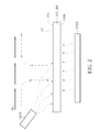
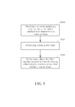
- FIG. 1 is a flow chart of a method of forming a thin film poly silicon layer according to a first preferred embodiment of the present invention
- FIG. 2 is a schematic diagram illustrating the method of this embodiment.
- the first preferred embodiment of the present invention provides a method of forming a thin film poly silicon layer.
- the method of forming the thin film poly silicon layer includes the following steps. Firstly, in step S110, a substrate 110 is provided.
- the substrate 110 has a first surface 110A and a second surface 110B.
- the substrate 110 in this embodiment may preferably include a substrate basis 110M.
- the substrate basis 110M may preferably include a glass substrate basis, a ceramic substrate basis, or other substrate bases made of appropriate materials.
- a heating treatment is performed.
- the heating treatment in this embodiment includes heating the substrate 110 to a temperature higher than 450 degrees Celsius by a heating source H.
- the heating treatment is used to heat the substrate 110 to a temperature higher than 500 degrees Celsius by the heating source H.
- the heating source H may preferably include a light heating source, an ion beam heating source, an electrode beam heating source, a furnace tube heating source and/or a filament heating source.
- the heating source H of this embodiment may preferably include a main heating source H1 and an auxiliary heating source H2.
- the heating treatment mentioned above may preferably include heating the substrate 110 to a first temperature by the main heating source H1, and heating the first surface 110A of the substrate 110 to a second temperature by the auxiliary heating source H2, but is not limited thereto.
- the second temperature is preferably higher than the first temperature.
- the first temperature is preferably higher than 200 degrees Celsius.
- the second temperature is higher than 450 degrees Celsius, and the second temperature is preferably higher than 500 degrees Celsius.
- step S130 a silicon thin film deposition process is then performed for directly forming a thin film poly silicon layer 120 on the first surface 110A of the substrate 110. Because the first surface 110A of the substrate 110 is heated to a temperature which is high enough for directly forming a thin film poly silicon layer, the thin film poly silicon layer 120 may be directly formed on the first surface 110A accordingly.
- the silicon thin film deposition process of this embodiment is preferably a chemical vapor deposition (CVD) process, such as a plasma enhanced chemical vapor deposition (PECVD) process, a metal-organic chemical vapor deposition (MOCVD) process, or a low pressure chemical vapor deposition (LPCVD) process, but is not limited thereto.
- CVD chemical vapor deposition
- PECVD plasma enhanced chemical vapor deposition
- MOCVD metal-organic chemical vapor deposition
- LPCVD low pressure chemical vapor deposition
- a reactive gaseous material RG is used to provide a source of silicon, and a thin film silicon layer may be formed on the first surface 110A of the substrate 110.
- the reactive gaseous material RG preferably includes silane (SiH 4 ) and/or dichlorosilane (SiH 2 Cl 2 ), which may be dissociated for forming the thin film silicon layer on the substrate 110.
- silane SiH 4
- dichlorosilane SiH 2 Cl 2
- the thin film poly silicon layer 120 may be directly formed on the first surface 110A of the substrate 110.
- Other crystallization processes such as a laser annealing process after the silicon thin film deposition process are not required in this embodiment.
- the method of forming the thin film poly silicon layer in this embodiment has advantages such as reduced process time, lower cost, and higher manufacturing efficiency. Additionally, the uniformity of the thin film poly silicon layer formed by the method of this embodiment is improved because the thin film poly silicon layer 120 is directly formed by the silicon thin film deposition process. The method of forming the thin film poly silicon layer in this embodiment is thus suitable for large area and size substrates.
- the auxiliary heating source H2 may also be selectively employed to continuously heat the first surface 110A and the deposited thin film silicon layer in an initial stage or other periods of the silicon thin film deposition process so as to further improve the crystallization quality of the thin film poly silicon layer 120.
- the auxiliary heating source H2 in this embodiment may preferably include a high energy heating source such as a light heating source, an ion beam heating source, an electrode beam heating source, a furnace tube heating source and/or a filament heating source
- the main heating source H1 in this embodiment may preferably include a susceptor heating source, a radio frequency (RF) heating source, and/or a infrared (IR) heating source.
- RF radio frequency
- IR infrared
- Other appropriate heating sources may also be selectively employed as the main heating source H1 and the auxiliary heating source H2 according to different heating considerations.
- the first surface 110A of the substrate 110 is mainly heated to the second temperature for forming the thin film poly silicon layer 120. Other parts of the substrate 110 are not required to be heated to the second temperature and thus the heat resistant properties of the substrate 110 may not be of consequence to the invention according to this embodiment.
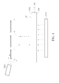
- FIG. 3 is a schematic diagram illustrating a method of forming a thin film poly silicon layer according to a second preferred embodiment of the present invention.
- the difference between the method of forming the thin film poly silicon layer in this embodiment and the method of the first preferred embodiment is that the silicon thin film deposition process of this embodiment is preferably a physical vapor deposition (PVD) process, and a silicon source SS such as a silicon target may be employed for sputtering a silicon layer on the first surface 110A of the substrate 110.
- PVD physical vapor deposition
- a thin film poly silicon layer 220 may be directly formed on the first surface 110A of the substrate 110.
- Other crystallization processes after the silicon thin film deposition process are not required in this embodiment.
- the other components, allocations, material properties, and the heating treatment in this embodiment are similar to those of the method of forming the thin film poly silicon layer in the first preferred embodiment detailed above and will not be described here again.
- the auxiliary heating source H2 may also be selectively employed to continuously heat the first surface 110A and the deposited thin film silicon layer in an initial stage or other periods of the silicon thin film deposition process so as to further improve the crystallization quality of the thin film poly silicon layer 220.
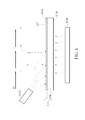
- FIG. 4 is a schematic diagram illustrating a method of forming a thin film poly silicon layer according to a third preferred embodiment of the present invention.
- a reactive gaseous material RG is preferably employed for forming the thin film poly silicon layer 120 on the first surface 110A of the substrate.
- the reactive gaseous material RG preferably includes silane and/or dichlorosilane, but is not limited thereto.
- the heating treatment in this embodiment may preferably include heating the substrate 110 to a first temperature by the main heating source H1, and heating the reactive gaseous material RG to a second temperature by the auxiliary heating source H2.
- the second temperature is preferably higher than the first temperature.
- the first temperature is preferably higher than 200 degrees Celsius
- the second temperature is higher than 450 degrees Celsius
- the second temperature is preferably higher than 500 degrees Celsius. Because the reactive gaseous material RG is already heated to the second temperature, which is high enough for directly forming a thin film poly silicon layer, by the auxiliary heating source H2, the thin film poly silicon layer 120 may be directly formed on the first surface 110A of the substrate 110.
- the auxiliary heating source H2 in this embodiment may preferably include a high energy heating source such as a light heating source, an ion beam heating source, an electrode beam heating source, a furnace tube heating source and/or a filament heating source, but is not limited thereto.
- a high energy heating source such as a light heating source, an ion beam heating source, an electrode beam heating source, a furnace tube heating source and/or a filament heating source, but is not limited thereto.
- the other components and material properties in this embodiment are similar to those of the method of forming the thin film poly silicon layer in the first preferred embodiment detailed above and will not be described here again.
- the auxiliary heating source H2 may also be employed to heat both the first surface 110A of the substrate 110 and the reactive gaseous material RG so as to further enhance the crystallization quality of the thin film poly silicon layer 120.
- FIG. 5 is a schematic diagram illustrating a method of forming a thin film poly silicon layer according to a fourth preferred embodiment of the present invention.
- the silicon thin film deposition process of this embodiment is preferably a physical vapor deposition process
- the silicon source SS such as a silicon target is employed for sputtering a silicon layer on the first surface 110A of the substrate 110.
- the heating treatment of this embodiment may preferably include heating the substrate 110 to a first temperature by the main heating source H1, and heating the silicon source SS in a stage before forming a silicon layer on the first surface 110A to a second temperature by the auxiliary heating source H2.
- the second temperature is preferably higher than the first temperature.
- the first temperature is preferably higher than 200 degrees Celsius
- the second temperature is higher than 450 degrees Celsius
- the second temperature is preferably higher than 500 degrees Celsius. Because the silicon source SS in the stage before forming the silicon layer on the first surface 110A is already heated to the second temperature, which is high enough for directly forming a thin film poly silicon layer, by the auxiliary heating source H2, the thin film poly silicon layer 220 may be directly formed on the first surface 110A of the substrate 110.
- the auxiliary heating source H2 in this embodiment may preferably include a high energy heating source such as a light heating source, an ion beam heating source, an electrode beam heating source, a furnace tube heating source and/or a filament heating source, but is not limited thereto.
- a high energy heating source such as a light heating source, an ion beam heating source, an electrode beam heating source, a furnace tube heating source and/or a filament heating source, but is not limited thereto.
- the other components and material properties in this embodiment are similar to those of the method of forming the thin film poly silicon layer in the second preferred embodiment detailed above and will not be described here again.
- the auxiliary heating source H2 may also be employed to heat both the first surface 110A of the substrate 110 and the silicon source SS in the stage before forming the silicon layer on the first surface 110A to the second temperature so as to further enhance the crystallization quality of the thin film poly silicon layer 220.
- FIG. 6 is a schematic diagram illustrating a method of forming a thin film poly silicon layer according to a fifth preferred embodiment of the present invention.
- a substrate 310 in this embodiment include the substrate base 110M and a heating auxiliary layer 311.
- the heating auxiliary layer 311 is disposed on the substrate basis 110M.
- the substrate 310 has a first surface 310A and a second surface 31 0B In other words, a surface of the heating auxiliary layer ⁇ 311 opposite to the substrate basis 110M may be regarded as the first surface 310A of the substrate 310.
- the heating auxiliary layer 311 is used to enhance heating efficiency of the heating source H2, and related process conditions may be further improved.
- the heating auxiliary layer 311 is made of a material with high endothermal efficiency.
- the heating auxiliary layer 311 may preferably include graphite, chromium oxide, and/or molybdenum, but is not limited thereto. Because of the heating auxiliary layer 311, the first surface 310A of the substrate 310 may be heated more efficiently to the second temperature, which is high enough for directly forming a thin film poly silicon layer, by the auxiliary heating source H2, and a thin film poly silicon layer 320 may be directly formed on the first surface 310A of the substrate 310. Other crystallization processes after the silicon thin film deposition process are not required in this embodiment.
- FIG. 7 is a schematic diagram illustrating a method of forming a thin film poly silicon layer according to a sixth preferred embodiment of the present invention.
- the silicon thin film deposition process of this embodiment is preferably a physical vapor deposition process
- the silicon source SS such as a silicon target is employed for sputtering a silicon layer on the first surface 310A of the substrate 310.
- the heating auxiliary layer 311 is used in this embodiment, and the first surface 310A of the substrate 310 may be accordingly heated more efficiently to the second temperature, which is high enough for directly forming a thin film poly silicon layer, by the auxiliary heating source H2.
- the thin film poly silicon layer 320 may be directly formed on the first surface 310A of the substrate 310. Other crystallization processes after the silicon thin film deposition process are not required in this embodiment.
- FIG. 8 is a flow chart of a method of forming a thin film poly silicon layer according to a seventh preferred embodiment of the present invention
- FIG. 9 is a schematic diagram illustrating the method of this embodiment.
- the seventh preferred embodiment of the present invention provides a method of forming a thin film poly silicon layer.
- the method of forming the thin film poly silicon layer includes the following steps. Firstly, in step S510, a substrate 510 is provided.
- the substrate 510 has a first surface 510A and a second surface 510B.
- the substrate 510 in this embodiment may preferably include a substrate basis 110M and a lattice matching layer 512.
- the lattice matching layer 512 is disposed on the substrate basis 110M.
- a surface of the lattice matching layer 512 opposite to the substrate basis 110M may be regarded as the first surface 510A of the substrate 510.
- the lattice matching layer 512 may preferably include a polymer material having a specific lattice direction, an amorphous silicon material and/or a metal oxide material having a specific lattice direction, such as zirconium oxide (ZrO2), cerium oxide (CeO2), praseodymium oxide (PrO2), and/or yttrium oxide (Y2O3), but is not limited thereto.
- ZrO2 zirconium oxide
- CeO2 cerium oxide
- PrO2 praseodymium oxide
- Y2O3 yttrium oxide
- a silicon thin film deposition process is performed for directly forming a thin film poly silicon layer 520 on the first surface 510A of the substrate 510.
- the heating treatment may preferably include heating the substrate 510 to a first temperature by the main heating source H1. It is worth noting that the first temperature may be between 150 degrees Celsius and 250 degrees Celsius because of the lattice matching layer 512 in the substrate 510.
- the silicon thin film deposition process of this embodiment is preferably a chemical vapor deposition process, such as a plasma enhanced chemical vapor deposition process, a metal-organic chemical vapor deposition process, or a low pressure chemical vapor deposition process, but is not limited thereto.
- FIG. 10 is a flow chart of a method of forming a thin film poly silicon layer according to an eighth preferred embodiment of the present invention
- FIG. 11 is a schematic diagram illustrating the method of this embodiment.
- the difference between the method of forming the thin film poly silicon layer in this embodiment and the method of the seventh preferred embodiment is that a heating treatment is performed in step S522 after the step S510 in this embodiment.
- the heating treatment mentioned above includes heating the substrate 510 to a temperature higher than 250 degrees Celsius by a heating source H.
- the heating source H may preferably include a main heating source H1 and an auxiliary heating source H2.
- the heating treatment may preferably include heating the substrate 510 to a first temperature by the main heating source H1, and heating the first surface 510A of the substrate 510 to a second temperature by the auxiliary heating source H2. Additionally, the second temperature is preferably higher than the first temperature. For example, the first temperature is preferably higher than 150 degrees Celsius, and the second temperature is preferably higher than 250 degrees Celsius. Subsequently, in step S530, a silicon thin film deposition process is then performed for directly forming a thin film poly silicon layer 620 on the first surface 510A of the substrate 510.
- the other components, allocations, material properties, and the silicon thin film deposition process in this embodiment are similar to those of the method of forming the thin film poly silicon layer in the seventh preferred embodiment detailed above and will not be described here again.
- the auxiliary heating source H2 may also be selectively employed to continuously heat the first surface 510A, the lattice matching layer 512, and the deposited thin film silicon layer in an initial stage or other periods of the silicon thin film deposition process so as to further improve the crystallization quality of the thin film poly silicon layer 620.
- the auxiliary heating source H2 in this embodiment may preferably include a high energy heating source such as a light heating source, an ion beam heating source, an electrode beam heating source, a furnace tube heating source and/or a filament heating source
- the main heating source H1 in this embodiment may preferably include a susceptor heating source, a radio frequency heating source, and/or a infrared heating source, but the present invention is not limited to this.
- Other appropriate heating sources may also be selectively employed as the main heating source H1 and the auxiliary heating source H2 for different heating considerations.
- the heating temperature of the first surface 510A may be further lowered because of the lattice matching layer 512 in the substrate 510 and thus the heat resistant properties of the substrate 510 may not be of consequence to the invention according to this embodiment.
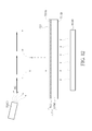
- FIG. 12 is a schematic diagram illustrating a method of forming a thin film poly silicon layer according to a ninth preferred embodiment of the present invention.
- the silicon thin film deposition process of this embodiment may preferably include using a reactive gaseous material RG to form the thin film poly silicon layer 620 on the first surface 510A of the substrate 510.
- the reactive gaseous material RG may preferably include silane and/or dichlorosilane, but is not limited thereto.
- the heating treatment in this embodiment may preferably include heating the substrate 510 to a first temperature by the main heating source H1, and heating the reactive gaseous material RG to a second temperature by the auxiliary heating source H2.
- the second temperature is preferably higher than the first temperature.
- the first temperature is preferably higher than 150 degrees Celsius
- the second temperature is preferably higher than 250 degrees Celsius, but is not limited thereto. Because of the lattice matching layer 512 in the substrate 510, the reactive gaseous material RG may be heated to a relatively low temperature for directly forming the thin film poly silicon layer 620 on the first surface 510A of the substrate 510.
- the auxiliary heating source H2 in this embodiment may preferably include a high energy heating source such as a light heating source, an ion beam heating source, an electrode beam heating source, a furnace tube heating source and/or a filament heating source, but is not limited thereto.
- a high energy heating source such as a light heating source, an ion beam heating source, an electrode beam heating source, a furnace tube heating source and/or a filament heating source, but is not limited thereto.
- the other components and material properties in this embodiment are similar to those of the method of forming the thin film poly silicon layer in the eighth preferred embodiment detailed above and will not be redundantly described.
- the auxiliary heating source H2 may also be employed to heat both the first surface 510A of the substrate 110 and the reactive gaseous material RG to the second temperature so as to further enhance the crystallization quality of the thin film poly silicon layer 620.
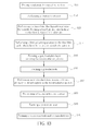
- FIG. 13 is a flow chart of a method of forming a thin film transistor according to a tenth preferred embodiment of the present invention.
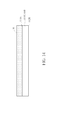
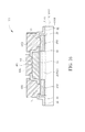
- FIGs. 14-16 are schematic diagrams illustrating the method of forming the thin film transistor in this embodiment. As shown in FIGs. 13-16 , this embodiment provides a method of forming a thin film transistor. The method of forming the thin film transistor includes the following steps. Firstly, in step S11, a substrate 110 is provided. The substrate 110 has a first surface 110A and a second surface 110B. Additionally, the substrate 110 in this embodiment may preferably include a substrate basis 110M. Subsequently, in step S12, a heating treatment is performed.
- a silicon thin film deposition process is then performed for directly forming a thin film poly silicon layer 20 on the first surface 110A of the substrate 110.
- the forming method of the thin film poly silicon layer 20 may be chosen from the methods of forming the thin film poly silicon layer in the first to the ninth preferred embodiments of the present invention described above.
- the heating approach, the heating temperature range, the silicon thin film deposition process, the process conditions and the material properties in this embodiment are similar to those of the methods of forming the thin film poly silicon layer in the first to ninth preferred embodiments detailed above and will not be described here again.
- a heating auxiliary layer (not shown) or/and a lattice matching layer (not shown) may be selectively applied as the embodiments described above, but is not limited thereto.
- step S14 a first patterning process is then performed on the thin film poly silicon layer 20 so as to form a semiconductor pattern 20P.
- step S15 a gate insulation layer 30 is formed to cover the semiconductor pattern 20P and the substrate 110.
- step S16 a gate electrode 40G is then formed on the gate insulation layer 30.
- the gate insulation layer 30 in this embodiment is formed after the first patterning process, and the gate electrode 40G is formed after the gate insulation layer 30 is formed.
- step S17 an ion implantation process is then performed after the gate electrode 40G is formed so as to form a plurality of doped regions 20D in the semiconductor pattern 20P.
- the doped regions 20D in this embodiment are preferably p-type doped poly silicon materials, but is not limited thereto.
- the gate electrode 40G may preferably be used as a shadow mask in the ion implantation process mentioned above so as to simplify the related processes and generate a self-aligned effect, but is not limited thereto.
- the method of forming the thin film transistor may further include performing a thermal activation process in step S18 after the ion implantation process in the step S17, and the thermal activation process is configured to activate the doped regions 20D.
- the thermal activation process may preferably include a light heating approach, an ion beam heating approach, an electrode beam heating approach, a furnace tube heating approach and/or a filament heating approach, but is not limited thereto.
- a protection layer 50 is formed on the gate insulation layer 30 and the gate electrode 40G.
- a plurality of first openings V1 are then formed in the protection layer 50 and the gate insulation layer 30.
- the first openings V1 partially expose the doped regions 20D.
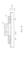
- a source electrode 60S and a drain electrode 60D are then formed in step S20 so as to form a thin film transistor T1 in FIG. 16 .
- the source electrode 60S and the drain electrode 60D contact the doped region 20D for being electrically connected with the doped region 20D via the first openings V1.
- a third opening V3 may be formed in the protection layer 50 when forming the first openings V1.
- the third opening V3 at least partially exposes the gate electrode 40G, but is not limited thereto.
- an auxiliary electrode 60G may be selectively formed in the step of forming the source electrode 60S and the drain electrode 60D.
- the auxiliary electrode 60G may contact and be electrically connected with the gate electrode 40G via the third opening V3.
- the source electrode 60S, the drain electrode 60D, and the auxiliary electrode 60G may be formed simultaneously by patterning a conductive layer, but is not limited thereto.
- the thin film transistor T1 may be regarded as a top gate poly silicon thin film transistor.
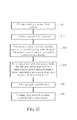
- FIG. 17 is a flow chart of a method of forming a thin film transistor according to an eleventh preferred embodiment of the present invention.
- FIGs. 18-20 are schematic diagrams illustrating the method of forming the thin film transistor in this embodiment.
- the difference between the method of forming the thin film transistor in this embodiment and the method of the tenth preferred embodiment is that the thin film poly silicon layer 20 and a doped layer 21 are directly formed on the first surface 110A of the substrate 110 in step S23 after the step S12.
- the dope layer 21 is formed on the thin film poly silicon layer 20.
- the doped layer 21 and the thin film poly silicon layer 20 are preferably formed in one identical silicon thin film deposition process so as to simplify the related processes, but is not limited thereto.
- the doped layer 21 in this embodiment may preferably include a p-type doped poly silicon material, but is not limited thereto.
- a first patterning process is then performed on the thin film poly silicon layer 20 to form a semiconductor pattern 20P, and a second patterning process is performed on the doped layer 21 to form a patterned doped layer 21 P.
- the first patterning process and the second patterning process are preferably integrated in one photo lithography etching process for process simplification purposes, but is not limited thereto.
- the first patterning process and the second patterning process may also be performed separately according to considerations beyond the scope of this invention.
- a gate insulation layer 32 is formed after the second patterning process, and the gate insulation layer 32 covers the semiconductor pattern 20P and the patterned doped layer 21 P.
- the gate insulation layer 32 may preferably include a plurality of second openings V2, and the second openings V2 are used to at least partially expose the patterned doped layer 21 P.
- a thin film transistor T2 as shown in FIG. 20 is then formed after forming a gate electrode 40G, a source electrode 40S, and a drain electrode 40D.
- the gate electrode 40G, the source electrode 40S, and the drain electrode 40D are formed after the gate insulation layer 32 is formed.
- the gate electrode 40G, the source electrode 40S, and the drain electrode 40D are preferably formed by one identical process step so as to simplify the process.
- the gate electrode 40G, the source electrode 40S and the drain electrode 40D may be simultaneously formed by patterning one conductive layer, but is not limited thereto.
- the doped layer 21 and the thin film poly silicon layer 20 may be formed by one identical process, an additional ion implantation process is not required in this embodiment. The purposes of process simplification and manufacturing cost reduction may thus be achieved.
- FIG. 21 is a flow chart of a method of forming a thin film transistor according to a twelfth preferred embodiment of the present invention.
- FIG. 22 and FIG. 23 are schematic diagrams illustrating the method of forming the thin film transistor in this embodiment. As shown in FIGs. 21-23 , the difference between the method of forming the thin film transistor in this embodiment and the method of the eleventh preferred embodiment is that a first patterning process is performed on a thin film poly silicon layer 20 to form a semiconductor pattern 20P in step S34 after the step S23.
- a source electrode 43S and a drain electrode 43D are formed on the doped layer 21, and a second patterning process is then performed on the doped layer 21 to form a patterned doped layer 21 P.
- the second patterning process and the process of forming the source electrode 43S and the drain electrode 43D are preferably integrated in one photo lithography etching process for process simplification purpose, but is not limited thereto.
- the patterned doped layer 21 P, the source electrode 43S, and the drain electrode 43D are preferably formed by an identical process step.
- the second patterning process may also be performed after the source electrode 43S and the drain electrode 43D are formed according to considerations beyond the scope of this invention.
- the source electrode 43S and the drain electrode 43D may preferably be used as a shadow mask in the second patterning process mentioned above so as to simplify the related processes, but is not limited thereto.
- a gate insulation layer 33 is formed after the second patterning process.
- the gate insulation layer 33 covers the source electrode 43S, the drain electrode 43D, the patterned doped layer 21 P and the semiconductor pattern 20P.
- the gate insulation layer 33 includes a plurality of second openings V4, and the second openings V4 are used to at least partially expose the source electrode 43S and the drain electrode 43D.
- a thin film transistor T3 as shown in FIG. 23 is formed after a gate electrode 53G is formed on the gate insulation layer 33.
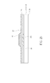
- FIG. 24 is a flow chart of a method of forming a thin film transistor according to a thirteenth preferred embodiment of the present invention.
- FIG. 25 and FIG. 26 are schematic diagrams illustrating the method of forming the thin film transistor in this embodiment.
- the method of forming the thin film transistor in this embodiment includes the following steps. Firstly, in step S41, a substrate 110 is provided. The substrate 110 has a first surface 110A and a second surface 110B. Subsequently, in step S42, a gate electrode 44G is formed on the substrate 110. A gate insulation layer 34 is then formed in step S43, and the gate insulation layer 34 covers the gate electrode 44G and the substrate 110. In step S44, a heating treatment is performed.
- a silicon thin film deposition process is then performed for directly forming a thin film poly silicon layer 22 and a doped layer 23 on the substrate 110.
- the forming method of the thin film poly silicon layer 22 may be chosen from the methods of forming the thin film poly silicon layer in the first to the ninth preferred embodiments of the present invention described above.
- the heating approach, the heating temperature range, the silicon thin film deposition process, the process conditions and the material properties in this embodiment are similar to those of the methods of forming the thin film poly silicon layer in the first to ninth preferred embodiments detailed above and will not be described here again.
- a heating auxiliary layer (not shown) or/and a lattice matching layer (not shown) may be selectively applied as the embodiments described above, but is not limited thereto.
- the doped layer 23 in this embodiment is preferably p-type doped poly silicon material, but is not limited thereto.
- a first patterning process is performed on the thin film poly silicon layer 22 to form a semiconductor layer 22P in step S46.
- a source electrode 64S and a drain electrode 64D are formed, and a second patterning process is then performed on the doped layer 23 to form a patterned doped layer 23P and a thin film transistor T4 as shown in FIG. 26 .
- the gate electrode 44G and the gate insulation layer 34 are formed before the thin film poly silicon layer 22 and the doped layer 23 are formed.
- the source electrode 64S and the drain electrode 64D are formed after the thin film poly silicon layer 22 and the doped layer 23 are formed.
- the thin film transistor T4 in this embodiment may be regarded as a bottom gate poly silicon thin film transistor. It is worth noting that the patterned doped layer 23P, the source electrode 64S, and the drain electrode 64D are preferably formed by an identical process step. In other words, the second patterning process and the process of forming the source electrode 64S and the drain electrode 64D are preferably integrated in one photo lithography etching process for process simplification purpose, but is not limited thereto.
- FIG. 27 is a schematic diagram illustrating a method of forming the thin film transistor according to a fourteenth preferred embodiment of the present invention.
- the difference between the method of forming the thin film transistor in this embodiment and the method of the thirteenth preferred embodiment is that the method of forming the thin film transistor in this embodiment further includes forming an etching stop layer 74 on the semiconductor pattern 22P.
- the etching stop layer 74 is formed before the doped layer 23 is formed, and the patterned doped layer 23P at least partially covers the etching stop layer 74.
- the etching stop layer 74 may be used to protect the semiconductor pattern 22P from being damaged during the process of forming the patterned doped layer 23P.
- the tolerance of process variations in the second patterning process may be thus enhanced, and an electrically performance of a thin film transistor T5 as shown in FIG. 27 may also be enhanced.
- the substrate or the process environment is heated to the temperature which is high enough for directly forming the thin film poly silicon layer, and the silicon thin film deposition process is performed to form the thin film poly silicon layer on the substrate.
- the silicon thin film deposition process is performed to form the thin film poly silicon layer on the substrate.
- other crystallization processes after the silicon thin film deposition process are thus not required.
- the method of forming the thin film poly silicon layer in the present invention has advantages such as reduced process time, lower cost, and higher manufacturing efficiency.
- the heating auxiliary layer and/or the lattice matching layer may be disposed in the substrate for further enhancing the heating efficiency on the surface of the substrate and further improving the crystallization quality of the thin film poly silicon layer.
- the method of forming the thin film poly silicon layer in the present invention may be used in a method of forming a thin film transistor, and purposes of process simplification and manufacturing cost reduction may thus be achieved.
Landscapes
- Chemical & Material Sciences (AREA)
- Engineering & Computer Science (AREA)
- Organic Chemistry (AREA)
- Materials Engineering (AREA)
- Metallurgy (AREA)
- Mechanical Engineering (AREA)
- Chemical Kinetics & Catalysis (AREA)
- General Chemical & Material Sciences (AREA)
- Inorganic Chemistry (AREA)
- Crystallography & Structural Chemistry (AREA)
- Thin Film Transistor (AREA)
- Recrystallisation Techniques (AREA)
- Microelectronics & Electronic Packaging (AREA)
Applications Claiming Priority (3)
| Application Number | Priority Date | Filing Date | Title |
|---|---|---|---|
| TW101120669 | 2012-06-08 | ||
| TW101125823A TWI506171B (zh) | 2012-06-08 | 2012-07-18 | 形成多晶矽薄膜之方法 |
| TW101136512A TW201415637A (zh) | 2012-10-03 | 2012-10-03 | 形成多晶矽薄膜之方法以及形成薄膜電晶體之方法 |
Publications (2)
| Publication Number | Publication Date |
|---|---|
| EP2671965A2 true EP2671965A2 (de) | 2013-12-11 |
| EP2671965A3 EP2671965A3 (de) | 2014-03-12 |
Family
ID=48625804
Family Applications (1)
| Application Number | Title | Priority Date | Filing Date |
|---|---|---|---|
| EP13171120.2A Withdrawn EP2671965A3 (de) | 2012-06-08 | 2013-06-07 | Verfahren zur Herstellung einer dünnschichtigen Polysiliziumschicht und Verfahren zur Bildung eines Dünnschichttransistors |
Country Status (2)
| Country | Link |
|---|---|
| US (1) | US8951921B2 (de) |
| EP (1) | EP2671965A3 (de) |
Cited By (1)
| Publication number | Priority date | Publication date | Assignee | Title |
|---|---|---|---|---|
| WO2018076139A1 (zh) * | 2016-10-24 | 2018-05-03 | 丁欣 | 多晶硅的制造方法以及单晶硅的制造方法 |
Families Citing this family (1)
| Publication number | Priority date | Publication date | Assignee | Title |
|---|---|---|---|---|
| US11232948B2 (en) | 2016-04-01 | 2022-01-25 | Intel Corporation | Layered substrate for microelectronic devices |
Family Cites Families (15)
| Publication number | Priority date | Publication date | Assignee | Title |
|---|---|---|---|---|
| GB2193976B (en) * | 1986-03-19 | 1990-05-30 | Gen Electric Plc | Process for depositing a polysilicon film on a substrate |
| DE69331659T2 (de) | 1993-01-13 | 2002-09-12 | Applied Materials Inc | Verfahren zur Abscheidung von Polysiliziumschichten mit einer verbesserten Uniformität und dazugehörige Vorrichtung |
| US5523587A (en) | 1993-06-24 | 1996-06-04 | At&T Corp. | Method for low temperature growth of epitaxial silicon and devices produced thereby |
| NL1004886C2 (nl) * | 1996-12-23 | 1998-06-24 | Univ Utrecht | Halfgeleiderinrichtingen en werkwijze voor het maken daarvan. |
| US6281098B1 (en) * | 1999-06-15 | 2001-08-28 | Midwest Research Institute | Process for Polycrystalline film silicon growth |
| US6841433B2 (en) * | 2001-12-29 | 2005-01-11 | Lg.Philips Lcd Co., Ltd. | Method of fabricating polysilicon thin film transistor |
| EP1403918A1 (de) * | 2002-09-25 | 2004-03-31 | Corning Incorporated | Halbleitervorrichtung und Herstellungsverfahren |
| TW594999B (en) * | 2002-11-22 | 2004-06-21 | Toppoly Optoelectronics Corp | Structure of thin film transistor array and driving circuits |
| TWI399580B (zh) | 2003-07-14 | 2013-06-21 | 半導體能源研究所股份有限公司 | 半導體裝置及顯示裝置 |
| TWI224868B (en) * | 2003-10-07 | 2004-12-01 | Ind Tech Res Inst | Method of forming poly-silicon thin film transistor |
| KR20060032454A (ko) * | 2004-10-12 | 2006-04-17 | 삼성전자주식회사 | 다결정 실리콘 제조방법 |
| TWI262550B (en) * | 2005-10-14 | 2006-09-21 | Ind Tech Res Inst | Element with a low temperature poly-Si film, method of direct poly-Si deposition at low temperature and inductively-coupled plasma chemical vapor deposition |
| US7521341B2 (en) * | 2005-11-09 | 2009-04-21 | Industrial Technology Research Institute | Method of direct deposition of polycrystalline silicon |
| KR100818287B1 (ko) | 2007-01-10 | 2008-03-31 | 삼성전자주식회사 | 폴리 실리콘의 형성방법, 이 폴리 실리콘을 구비하는 박막트랜지스터 및 그 제조방법 |
| US8168467B2 (en) * | 2010-03-17 | 2012-05-01 | James P Campbell | Solar cell method of fabrication via float glass process |
-
2013
- 2013-06-07 EP EP13171120.2A patent/EP2671965A3/de not_active Withdrawn
- 2013-06-07 US US13/912,199 patent/US8951921B2/en not_active Expired - Fee Related
Non-Patent Citations (1)
| Title |
|---|
| None |
Cited By (1)
| Publication number | Priority date | Publication date | Assignee | Title |
|---|---|---|---|---|
| WO2018076139A1 (zh) * | 2016-10-24 | 2018-05-03 | 丁欣 | 多晶硅的制造方法以及单晶硅的制造方法 |
Also Published As
| Publication number | Publication date |
|---|---|
| US8951921B2 (en) | 2015-02-10 |
| EP2671965A3 (de) | 2014-03-12 |
| US20130330886A1 (en) | 2013-12-12 |
Similar Documents
| Publication | Publication Date | Title |
|---|---|---|
| US7704806B2 (en) | Thin film transistor having silicon nanowire and method of fabricating the same | |
| US10504946B2 (en) | Array substrate manufacturing method and array substrate | |
| US7919365B2 (en) | Fabrication methods of a ZnO thin film structure and a ZnO thin film transistor, and a ZnO thin film structure and a ZnO thin film transistor | |
| US10325938B2 (en) | TFT array substrate, method for manufacturing the same, and display device | |
| TWI497724B (zh) | 薄膜電晶體及其製造方法 | |
| CN103107095A (zh) | 薄膜晶体管及其制作方法、阵列基板、显示装置 | |
| US8501556B2 (en) | Thin film transistor formed on flexible substrate and method of manufacturing the same | |
| CN105655407A (zh) | 多晶硅薄膜晶体管及其制备方法、阵列基板、显示装置 | |
| US20060226425A1 (en) | Thin film transistor and method of fabricating the same | |
| US20160343874A1 (en) | Low temperature poly-silicon thin-film transistor and manufacturing method thereof | |
| US9252284B2 (en) | Display substrate and method of manufacturing a display substrate | |
| CN111341794A (zh) | 显示面板、阵列基板及其制作方法 | |
| US6812072B2 (en) | Method for crystallizing amorphous film and method for fabricating LCD by using the same | |
| CN108376691B (zh) | 显示面板和显示装置 | |
| US8951921B2 (en) | Method of forming thin film poly silicon layer and method of forming thin film transistor | |
| US20070254399A1 (en) | Low temperature direct deposited polycrystalline silicon thin film transistor structure and method for manufacturing the same | |
| US9136354B2 (en) | Methods for manufacturing passivation layer and thin film transistor array substrate | |
| TWI518430B (zh) | 顯示面板及應用其之顯示裝置 | |
| CN111987095B (zh) | 半导体元件及其制备方法 | |
| US20140087527A1 (en) | Method of forming thin film poly silicon layer and method of forming thin film transistor | |
| CN101789450B (zh) | 薄膜晶体管及制造富硅沟道层的方法 | |
| US6887745B2 (en) | Polysilicon thin film transistor and method of forming the same | |
| US20110068333A1 (en) | Pixel structure and method for manufacturing the same | |
| CN103489783A (zh) | 形成多晶硅薄膜的方法以及形成薄膜晶体管的方法 | |
| TW201415637A (zh) | 形成多晶矽薄膜之方法以及形成薄膜電晶體之方法 |
Legal Events
| Date | Code | Title | Description |
|---|---|---|---|
| PUAI | Public reference made under article 153(3) epc to a published international application that has entered the european phase |
Free format text: ORIGINAL CODE: 0009012 |
|
| AK | Designated contracting states |
Kind code of ref document: A2 Designated state(s): AL AT BE BG CH CY CZ DE DK EE ES FI FR GB GR HR HU IE IS IT LI LT LU LV MC MK MT NL NO PL PT RO RS SE SI SK SM TR |
|
| AX | Request for extension of the european patent |
Extension state: BA ME |
|
| PUAL | Search report despatched |
Free format text: ORIGINAL CODE: 0009013 |
|
| AK | Designated contracting states |
Kind code of ref document: A3 Designated state(s): AL AT BE BG CH CY CZ DE DK EE ES FI FR GB GR HR HU IE IS IT LI LT LU LV MC MK MT NL NO PL PT RO RS SE SI SK SM TR |
|
| AX | Request for extension of the european patent |
Extension state: BA ME |
|
| RIC1 | Information provided on ipc code assigned before grant |
Ipc: C23C 16/24 20060101ALI20140205BHEP Ipc: H01L 29/786 20060101ALI20140205BHEP Ipc: C23C 16/48 20060101ALI20140205BHEP Ipc: C23C 16/02 20060101ALI20140205BHEP Ipc: H01L 29/49 20060101ALI20140205BHEP Ipc: H01L 21/02 20060101ALI20140205BHEP Ipc: C23C 14/02 20060101ALI20140205BHEP Ipc: H01L 21/20 20060101ALI20140205BHEP Ipc: C23C 14/18 20060101AFI20140205BHEP Ipc: H01L 29/66 20060101ALI20140205BHEP Ipc: C30B 29/06 20060101ALI20140205BHEP |
|
| 17P | Request for examination filed |
Effective date: 20140909 |
|
| RBV | Designated contracting states (corrected) |
Designated state(s): AL AT BE BG CH CY CZ DE DK EE ES FI FR GB GR HR HU IE IS IT LI LT LU LV MC MK MT NL NO PL PT RO RS SE SI SK SM TR |
|
| STAA | Information on the status of an ep patent application or granted ep patent |
Free format text: STATUS: THE APPLICATION IS DEEMED TO BE WITHDRAWN |
|
| 18D | Application deemed to be withdrawn |
Effective date: 20141210 |