EP2657978A1 - Photoelectric converter and method for producing same - Google Patents
Photoelectric converter and method for producing same Download PDFInfo
- Publication number
- EP2657978A1 EP2657978A1 EP11857851.7A EP11857851A EP2657978A1 EP 2657978 A1 EP2657978 A1 EP 2657978A1 EP 11857851 A EP11857851 A EP 11857851A EP 2657978 A1 EP2657978 A1 EP 2657978A1
- Authority
- EP
- European Patent Office
- Prior art keywords
- transparent conductive
- conductive film
- film
- conversion unit
- photoelectric conversion
- Prior art date
- Legal status (The legal status is an assumption and is not a legal conclusion. Google has not performed a legal analysis and makes no representation as to the accuracy of the status listed.)
- Withdrawn
Links
Images

Classifications
-
- H—ELECTRICITY
- H10—SEMICONDUCTOR DEVICES; ELECTRIC SOLID-STATE DEVICES NOT OTHERWISE PROVIDED FOR
- H10F—INORGANIC SEMICONDUCTOR DEVICES SENSITIVE TO INFRARED RADIATION, LIGHT, ELECTROMAGNETIC RADIATION OF SHORTER WAVELENGTH OR CORPUSCULAR RADIATION
- H10F77/00—Constructional details of devices covered by this subclass
- H10F77/20—Electrodes
- H10F77/206—Electrodes for devices having potential barriers
- H10F77/211—Electrodes for devices having potential barriers for photovoltaic cells
- H10F77/219—Arrangements for electrodes of back-contact photovoltaic cells
-
- H—ELECTRICITY
- H10—SEMICONDUCTOR DEVICES; ELECTRIC SOLID-STATE DEVICES NOT OTHERWISE PROVIDED FOR
- H10F—INORGANIC SEMICONDUCTOR DEVICES SENSITIVE TO INFRARED RADIATION, LIGHT, ELECTROMAGNETIC RADIATION OF SHORTER WAVELENGTH OR CORPUSCULAR RADIATION
- H10F10/00—Individual photovoltaic cells, e.g. solar cells
- H10F10/10—Individual photovoltaic cells, e.g. solar cells having potential barriers
- H10F10/16—Photovoltaic cells having only PN heterojunction potential barriers
- H10F10/164—Photovoltaic cells having only PN heterojunction potential barriers comprising heterojunctions with Group IV materials, e.g. ITO/Si or GaAs/SiGe photovoltaic cells
- H10F10/165—Photovoltaic cells having only PN heterojunction potential barriers comprising heterojunctions with Group IV materials, e.g. ITO/Si or GaAs/SiGe photovoltaic cells the heterojunctions being Group IV-IV heterojunctions, e.g. Si/Ge, SiGe/Si or Si/SiC photovoltaic cells
- H10F10/166—Photovoltaic cells having only PN heterojunction potential barriers comprising heterojunctions with Group IV materials, e.g. ITO/Si or GaAs/SiGe photovoltaic cells the heterojunctions being Group IV-IV heterojunctions, e.g. Si/Ge, SiGe/Si or Si/SiC photovoltaic cells the Group IV-IV heterojunctions being heterojunctions of crystalline and amorphous materials, e.g. silicon heterojunction [SHJ] photovoltaic cells
-
- H—ELECTRICITY
- H10—SEMICONDUCTOR DEVICES; ELECTRIC SOLID-STATE DEVICES NOT OTHERWISE PROVIDED FOR
- H10F—INORGANIC SEMICONDUCTOR DEVICES SENSITIVE TO INFRARED RADIATION, LIGHT, ELECTROMAGNETIC RADIATION OF SHORTER WAVELENGTH OR CORPUSCULAR RADIATION
- H10F77/00—Constructional details of devices covered by this subclass
- H10F77/20—Electrodes
- H10F77/206—Electrodes for devices having potential barriers
- H10F77/211—Electrodes for devices having potential barriers for photovoltaic cells
- H10F77/215—Geometries of grid contacts
-
- H—ELECTRICITY
- H10—SEMICONDUCTOR DEVICES; ELECTRIC SOLID-STATE DEVICES NOT OTHERWISE PROVIDED FOR
- H10F—INORGANIC SEMICONDUCTOR DEVICES SENSITIVE TO INFRARED RADIATION, LIGHT, ELECTROMAGNETIC RADIATION OF SHORTER WAVELENGTH OR CORPUSCULAR RADIATION
- H10F77/00—Constructional details of devices covered by this subclass
- H10F77/20—Electrodes
- H10F77/244—Electrodes made of transparent conductive layers, e.g. transparent conductive oxide [TCO] layers
-
- Y—GENERAL TAGGING OF NEW TECHNOLOGICAL DEVELOPMENTS; GENERAL TAGGING OF CROSS-SECTIONAL TECHNOLOGIES SPANNING OVER SEVERAL SECTIONS OF THE IPC; TECHNICAL SUBJECTS COVERED BY FORMER USPC CROSS-REFERENCE ART COLLECTIONS [XRACs] AND DIGESTS
- Y02—TECHNOLOGIES OR APPLICATIONS FOR MITIGATION OR ADAPTATION AGAINST CLIMATE CHANGE
- Y02E—REDUCTION OF GREENHOUSE GAS [GHG] EMISSIONS, RELATED TO ENERGY GENERATION, TRANSMISSION OR DISTRIBUTION
- Y02E10/00—Energy generation through renewable energy sources
- Y02E10/50—Photovoltaic [PV] energy
Definitions
- the present invention relates to photoelectric converters and methods for producing the same.
- Patent Document 1 discloses a photoelectric converter which is provided with a photoelectric conversion unit, a light-receiving surface electrode provided on a light-receiving surface of the photoelectric conversion unit, and a rear surface electrode provided on the rear surface of the photoelectric conversion unit.
- each of the light-receiving surface electrode and the rear surface electrode is provided with two or more finger electrode units and two or more busbar electrode units connected to the finger electrode units.
- a photoelectric converter includes a photoelectric conversion unit; a light-receiving surface electrode disposed on a light-receiving surface of the photoelectric conversion unit; and a rear surface electrode disposed on a rear surface of the photoelectric conversion unit; wherein the rear surface electrode comprises a transparent conductive film layered on the rear surface of the photoelectric conversion unit; and a metal film layered on substantially the entire surface of the transparent conductive film except for an edge area.
- a method for manufacturing a photoelectric converter according to the present invention includes preparing a photoelectric conversion unit; placing a mask covering at least apart of an edge area on a photoelectric conversion unit and layering a transparent conductive film on an area on the photoelectric conversion unit except for the edge area covered by the mask; and with the transparent conductive film attached to the mask, a metal film is layered on an area on the transparent conductive film.
- a method for manufacturing a photoelectric converter according to the present invention may include preparing a photoelectric conversion unit; placing a first mask covering at least a part of an edge area on a photoelectric conversion unit and layering a transparent conductive film on an area on the photoelectric conversion unit except for the edge area which is covered by the first mask; and placing a second mask covering at least a part of an edge area on the transparent conductive film and layering a metal film on an area on the transparent conductive film except for the edge area covered by the second mask.
- a photoelectric converter having improved light conversion efficiency and a manufacturing method of the same are provided.
- a photoelectric converter 10 according to an embodiment of the present invention and a method for manufacturing the same are described below by referring to the drawings. It should be noted that the embodiments shown below are provided merely as examples. The present invention is not limited to the embodiments shownbelow. Further, the drawings referred to in the embodiments are schematically illustrated, and thus the dimensional ratios or the like shown in the drawings may be different from the dimensional ratios of the actual elements. Dimensional ratios or the like of a specific element should be determined by referring to the description below.
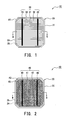
- FIG. 1 shows the photoelectric converter 10 viewed from a light-receiving surface side
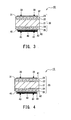
- FIG. 2 shows the photoelectric converter 10 viewed from a rear surface side of the photoelectric converter 10.
- the photoelectric converter 10 is provided with a photoelectric conversion unit 20 and a light-receiving surface electrode 30 provided on a light receiving surface of the photoelectric conversion unit 20, and a rear surface electrode 40 provided on a rear surface of the photoelectric conversion unit 20.
- the "light-receiving surface” indicates a main incident surface of light from outside of the converter. For example, when assembling a module such as a solar cell including the photoelectric converter 10, more than 50% to 100% of the incident light to the device comes from the light-receiving surface.
- the "rear surface” indicates a surface opposite the light-receiving surface.
- the photoelectric conversion unit 20 is a member to generate carriers (electrons and holes) by receiving light such as solar light.
- the carriers generated by the photoelectric conversion unit 20 are collected by the light-receiving surface electrode 30 and the rear surface electrode 40.
- the carriers are retrieved outside as electrical energy by assembling the photoelectric converter 10 in a module by electrically connecting wiring members (not shown) to the light-receiving surface electrode 30 and the rear surface electrode 40.
- the photoelectric conversion unit 20 is provided with an n-type single crystalline silicon substrate 21 which is a crystalline semiconductor substrate having a substantially square shape.
- the photoelectric conversion unit 20 is provided with a p-type amorphous silicon film 23 layered via an i-type amorphous silicon film 22.
- a transparent conductive film 31 included in the light-receiving surface electrode 30 is layered on the light-receiving surface of the p-type amorphous silicon film 23.
- finger electrode units 32 and busbar electrode units 33 for collecting electrical power generated by the photoelectric conversion unit 20 are formed on the transparent conductive film 31.
- the photoelectric conversion unit 20 is provided with an n-type amorphous silicon film 25 layered via an i-type amorphous silicon film 24.
- a transparent conductive film 41 included in the rear surface electrode 40 is layered on the rear surface of the n-type amorphous silicon film25.
- a metal film 42 for collecting electrical power generated by the photoelectric conversion unit 20 is formed on the transparent conductive film 41.
- Protruding electrodes 43 which are used as connecting units to the wire members are provided on the metal film 42.
- the photoelectric conversion unit 20 has a configuration in which amorphous semiconductor thin films are layered on both surfaces of a crystalline semiconductor substrate.
- the photoelectric conversion unit 20 has a layered configuration in which a p-type amorphous silicon film 23, i-type amorphous silicon film 22, n-type single crystal silicon substrate 21, i-type amorphous silicon film 24, and n-type amorphous silicon film 25 are layered in this order.
- the p-type amorphous silicon film 23 side is the light-receiving surface side.
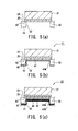
- FIG. 3 cross-sectional view taken along the line B-B in FIGs. 1 and 2 .
- the photoelectric conversion unit 20 is provided with the i-type amorphous silicon film 22 layered on the entire light-receiving surface of the n-type single crystal silicon substrate 21 and the i-type amorphous silicon film 24 layered on the entire rear surface of the n-type single crystal silicon substrate 21.
- the i-type amorphous silicon films 22, 24 may be layered on the entire light-receiving surface and the rear surface of the n-type single crystal silicon substrate 21 except for an edge area.
- the i-type amorphous silicon films 22, 24 are genuine amorphous silicon thin films having, for example, the same composition.
- the photoelectric conversion unit 20 is provided with the p-type amorphous silicon film 23 layered on the entire light-receiving surface of the i-type amorphous silicon film 22 and the n-type amorphous silicon film 25 layered on the entire rear surface of the i-type amorphous silicon film 24.
- the light-receiving surface and the rear surface of the photoelectric conversion unit 20 can be respectively formed as textured surfaces (not shown).
- the textured surface indicates an uneven surface which increases amount of light absorption by the photoelectric conversion unit 20 by restricting surface reflection.
- a specific example of the textured surface is an uneven surface having a pyramid shape (such as square pyramid and truncated pyramid) which can be obtained by applying anisotropic etching on the light-receiving surface and the rear surface of the n-type single crystal silicon substrate 21 having a (100) surface.
- the thickness of the photoelectric conversion unit 20 (the length of the film in the layered direction) is, for example, several hundred ⁇ m, most of which is the thickness of the n-type single crystal silicon substrate 21.
- the thickness of the amorphous silicon film is, for example, from several nm to several tens of nm.
- the height of unevenness of the texture structure is, for example, several ⁇ m. Therefore, the texture surface is reflected to the light-receiving surface and the rear surface of the amorphous silicon film.
- the light-receiving surface electrode 30 includes a transparent conductive film 31, two or more finger electrode units 32, and two or more busbar electrode units 33.
- the finger electrode units 32 and the busbar electrode units 33 are electrically connected to each other, and both are formed on the transparent conductive film 31. That is, in the light-receiving surface electrode 30, carriers transmitted from the p-type amorphous silicon film23 via the transparent conductive film 31 are collected by the finger electrode units 32 and the busbar electrode units 33.
- the photoelectric converter 10 is assembled in a module, the carriers collected by the busbar electrode units 33 which are electrically connected with the wire member are retrieved outside.
- the transparent conductive film 31 may be a thin film (TCO film) including at least one of metal oxides having a polycrystalline structure, such as indium oxide (In 2 O 3 ), zinc oxide (ZnO), tin oxide (SnO 2 ), and titanium oxide (TiO 2 ).
- the transparent conductive film 31 functions as a light transmissive electrode unit.
- a dopant such as tin (Sn), zinc (Zn), tungsten (W), antimony (Sb), titanium (Ti), aluminum (Al), cerium (Ce), and gallium (Ga) may be doped in the above metal oxides.
- the concentration of the dopant may be 0 to 20 wt%.
- the thickness of the transparent conductive film 31 may be, for example, 50 nm to 200 nm. It is preferable that the transparent conductive film 31 is layered on the entire surface region except for the edge area (hereinafter referred to as "edge area A1") on the light-receiving surface of the p-type amorphous silicon film 23. It is preferable that the edge area A1 on which the transparent conductive film 31 is not layered is a surface region having a width of about 1 to 2 mm from the edge of the light-receiving surface of the p-type amorphous silicon film 23, and provided annularly along the circumference of the light-receiving surface.
- the finger electrode units 32 and the busbar electrode units 33 are thin line electrode units formed from conductive paste made from binder resin in which conductive particles such as silver (Ag) are dispersed.
- the finger electrode units 32 and the busbar electrode units 33 are provided to collect electrical power generated by the photoelectric conversion unit 20 via the transparent conductive film 31.
- the finger electrode units 32 may be, for example, strip-shaped metal layers formed on the light-receiving surface so as to evenly collect electrical power from the entire photoelectric conversion unit 20. It is preferable that the finger electrode units 32 are positioned parallel to each other with intervening spaces of a predetermined length (for example, width of 100 ⁇ m, and an intervening space of 2 mm).
- the busbar electrode units 33 are provided to further collect the electrical power collected by the finger electrode units 32.
- the busbar electrode units 33 may be, for example, strip shaped metal layers formed on the light-receiving surface.
- the busbar electrode units 33 are positioned to intersect with the finger electrode units 32 to which the busbar electrode units 33 are electrically connected.
- the busbar electrode units 33 may be positioned, for example, parallel to each other with an intervening space of a predetermined length. It is preferable that the busbar electrode units 33 are arranged to be fewer and wider than the finger electrode units 32 (for example, width of 1.5mm, two pieces).
- the shapes of the finger electrode units 32 and the busbar electrode units 33 are not limited to the above mentioned shapes but various shapes such as a zigzag shape are also applicable.
- the rear surface electrode 40 includes the transparent conductive film 41, the metal film 42, and the two or more protruding electrodes 43.
- the protruding electrodes 43 are electrodes having a shape protruding in the direction of thickness of the photoelectric conversion unit 20 on the metal film 42.
- the wiring member is connected to the protruding electrodes 43.
- the protruding electrodes 43 may have a strip shape made from, for example, conductive paste on the metal film 42.
- two protruding electrodes 43 may be positioned parallel to each other with an intervening space of a predetermined length in the same direction as the busbar electrode units 33.
- the shape of the protruding electrodes 43 is not limited to the above mentioned shape but various shapes such as a dot shape and zigzag shape are also applicable (refer to FIGs. 7 and 8 described below).
- the transparent conductive film 41 may be formed from ITO, ZnO, SnO 2 , or the like, and function as a light transmissive electrode unit. Further, as described in detail below, the transparent conductive film 41 prevents direct contact between the photoelectric conversion unit 20 and the metal film 42 and functions to raise the reflection ratio by interacting with the metal film 42. It is preferable that the transparent conductive film 41 has a thickness of about 50 nm to 200 nm and that the previously described texture surface is also applied to the rear surface of the transparent conductive film 41.
- the transparent conductive film 41 is layered on the entire surface region except for the edge area (hereinafter referred to as "edge area A2") on the rear surface of the n-type amorphous silicon film 25. It is further preferable that the edge area A2 on which the transparent conductive film 41 is not layered is a surface region having a width of about 1 to 2 mm from the edge of the rear surface of the n-type amorphous silicon film 25, and provided annularly along the circumference of the rear surface.
- the metal film 42 is a thin film made from a metal material having a high light reflection ratio and a high conductivity.
- the metal film 42 preferably has a high reflection ratio for light in the infrared region.
- the reflection ratio of the metal film 42 is preferably higher than that of the transparent conductive film 41 at least for light in the infrared region.
- the metal film 42 functions as an electrode which collects carriers transmitted from the n-type amorphous silicon film 25 via the transparent conductive film 41.
- the metal film 42 further has a function to reflect, to the light-receiving surface side, transmitted light which has passed through the photoelectric conversion unit 20.
- the metal film 42 is preferably thick enough to prevent light from passing through and thin enough to reflect the texture surface to the rear surface.
- the metal film 42 preferably has a thickness of about 0.1 ⁇ m to 5 ⁇ m.
- Applicable metal material for the metal film 42 is a metal, for example, silver (Ag), aluminum (A1), titan (Ti), rhodium (Rh), copper (Cu), gold (Au), platinum (Pt), nickel (Ni), chrome (Cr), or an alloy including at least one of these metals. It is preferable that the metal material has a high reflective ratio to light in the infrared region, in particular, a wavelength of about 800 nm to 1200 nm.
- Ag, Al, Ti, Rh, Cu, and Au, and an alloy including at least one of these materials are preferable. Materials, Ag, Al, and Ti and an alloy including at least one of these materials are more preferable, and Ag and an alloy including Ag are particularly preferable.
- the metal film 42 may be formed by two or more layered films made from the above metal materials.
- a layered body of AG film and Al film may be regarded as an example.
- the Ag film is preferably positioned on the transparent conductive film 41 side.
- An Ag-Al-Ag layered body in which both sides of the Al film are layered by Ag films, or, for example, an Ag-Cu-Ag layered body in which another metal film (such as Cu film) is used in place of the Al film may be used.
- the metal film 42 may be layered on substantially the entire surface of the transparent conductive film 41 except for an edge area (hereinafter referred to as "edge area A3"). It is more preferable that the metal film 42 may be layered on the entire surface of the transparent conductive film 41 except for the edge area A3. It should be noted that “being layered on substantially the entire surface of the transparent conductive film 41 except for an edge area” includes a state where the metal film 42 can be recognized to be layered on substantially the entire surface of the transparent conductive film 41, which includes a case in which a part of the metal film 42 layered on the transparent conductive film 41 is missing. Specifically, a state where the metal film 42 covers more than 95% of the transparent conductive film 41 except for the edge area A3 can be raised as an example.
- the metal film 42 is layered in at least part of the edge area A3 of the transparent conductive film 41 such that the metal film 42 does not cover the n-type amorphous silicon film 25 across the transparent conductive film 41.
- the metal film 42 may be layered on a part of the edge area A3.
- the metal film 42 is layered so as not to cover the n-type amorphous silicon film 25 beyond the transparent conductive film 41 on the entire circumference of the edge region A3 of the transparent conductive film 41. That is, it is preferable that, on the rear surface of the transparent conductive film 41, the metal film 42 is layered on the entire surface or substantially the entire surface except for the edge area A3.
- the edge area A3 on which the metal film 42 is not layered is preferably narrow in consideration of reflection or the like of transmissive light.
- the edge area A3 has a width of 1 mm to 5 mm from the edge of the transparent conductive film 41.
- the edge area A3 is preferably provided annularly along the circumference of the rear surface of the transparent conductive film 41.
- the width of the edge area A3 can be checked by cross-sectional observation using a scanning electron microscope (SEM) or transmission electron microscope (TEM) (an optical microscope can also be used with a wide width).
- the metal film 42 comes into contact with the edge area A2 of the n-type amorphous silicon film 25 beyond at least a part of the edge area A3 of the transparent conductive film 41, an issue of carrier trap may occur because the metal atoms of the metal film 42 may diffuse into the n-type amorphous silicon film 25 in that region to cause a defect energy level.
- the metal film 42 is provided so as not to directly contact the rear surface of the photoelectric conversion unit 20 (n-type amorphous silicon film 25) via the transparent conductive film 41, it is possible to restrict occurrence of the defect energy level.
- the edge area A3 is provided annually along the entire circumference of the transparent conductive film 41 to avoid contact between the metal film 42 and the photoelectric conversion unit 20 (n-type amorphous silicon film 25) in the entire circumference of the photoelectric conversion unit 20. This results in restriction of the occurrence of the defect energy level.
- the photoelectric conversion unit 20 When the photoelectric conversion unit 20 is configured to include an amorphous silicon film layered on a single crystal silicon substrate, the effect of the defect energy level caused by metals diffused into the amorphous silicon film increases. In such a case, an achievable advantage by preventing contact between the photoelectric conversion unit 20 and the metal film 42 becomes significant.
- the metal film 42 is layered over a wide area of the rear surface of the photoelectric conversion unit 20 (n-type amorphous silicon film 25). In this way, the transmitted light that has entered from the light-receiving surface and passed through the photoelectric conversion unit 20 can be reflected to the light-receiving surface by the metal film 42. Therefore, the light absorption ratio at the photoelectric conversion unit 20 can be improved.
- the metal film 42 is layered on the photoelectric conversion unit 20 via the transparent conductive film 41. In this way, the reflection ratio of the metal film 42 increases because light absorption is restricted by the occurrence of evanescent light. It should be noted that a texture surface is also applied on the rear surface of the photoelectric conversion unit 20. Therefore, light scatters on the rear surface making it easier for the photoelectric conversion unit 20 to capture light.
- the transparent conductive film 41 has high adhesive properties with both of the photoelectric conversion unit 20 and the metal film 42. Therefore, it becomes possible to increase the adhesive strength (also known as peel strength) of the metal film 42.
- the transparent conductive film 41 has a protruding portion which covers a side surface of the metal film 42 in the edge area A2.
- the "side surface" of the metal film 42 indicates a surface along the thickness of the metal film 42.
- the shape having the protruding portion can be obtained by, for example, a method in FIG. 5 described below.
- the protruding portion has a width of about several nm to several hundred nm and a height (the length in the direction of thickness) of about the same as the metal film 42. In such a configuration, the same effects as mentioned above can be achieved.
- the i-type amorphous silicon film 24 is layered on the substrate by, for example, plasma-enhanced chemical vapor deposition (plasma CVD).
- plasma CVD plasma-enhanced chemical vapor deposition
- n-type amorphous silicon film 25 is layered on the i-type amorphous silicon film 24.
- the surface of the n-type single crystal silicon substrate 21 on which the n-type amorphous silicon film 25 is layered is the rear surface.
- silane gas (SiH 4 ) is used as source gas.
- n-type amorphous silicon film 25 for example, silane gas (SiH 4 ), hydrogen (H 2 ), or phosphine (PH 3 ) is used as source gas.
- silane gas SiH 4
- hydrogen H 2
- phosphine PH 3
- the i-type amorphous silicon film 22 and the p-type amorphous silicon film 23 can also be layered on the light receiving surface of the n-type single crystal silicon substrate 21 by the plasma CVD method.
- diborane (B 2 H 6 ) is used as the source gas in place of PH 3 .
- the finger electrode units 32 and the busbar electrode units 33 of the light-receiving surface electrode 30 can be formed by, for example, screen printing conductive paste in a desired pattern on the transparent conductive film 31.
- various method such as sputtering methods, evaporation methods, and plating methods may be applied.
- the transparent conductive film 31 can be layered by the same method for the transparent conductive film 41 (as described below).
- the process to manufacture the rear surface electrode 40 in particular, the layering process of the transparent conductive film 41 and the metal film 42 is described in detail below.
- a layer configuration of the n-type single crystal silicon substrate 21 on the light-receiving surface side is omitted.
- the film layered on the mask 50 is distinguished from the film layered on the rear surface of the n-type amorphous silicon film25byassigning "M" at the end of the reference numerals.
- FIG. 5 (a) indicates a state in which the mask 50 is disposed on the rear surface of the n-type amorphous silicon film 25.
- the mask 50 is disposed to cover the edge area A2 on the rear surface of the n-type amorphous silicon film 25.
- the transparent conductive film 41 is layered by, for example, a sputtering method on the rear surface of the n-type amorphous silicon film 25 on which the mask 50 has been disposed.
- a metal support frame which supports the n-type single crystal silicon substrate 21 from the rear surface may be used.
- FIG. 5(b) shows an intermediate body 11 in which the transparent conductive film 41 is layered on the entire surface of the n-type amorphous silicon film 25 except for the edge area A2.
- the transparent conductive film 41M is also attached to the mask 50.
- the transparent conductive film 41M is attached not only on the surface 51 of the mask 50, but also on a side surface 52 of an opening.
- the transparent conductive film 41M attached to the side surface 52 of the opening has a thickness of, for example, about several nm to several hundred nm and is formed continuously with the transparent conductive film 41.
- the metal film 42 is layered on the rear surface of the transparent conductive film 41 by, for example, a sputtering method.
- FIG. 5(c) shows an intermediate body 12 in which the metal film 42 is layered on the entire rear surface of the transparent conductive film 41 except for the edge area A3.
- the metal film 42M is also layered on the transparent conductive film 41M which is attached to the surface 51 and the side surface 52 of the opening.
- the metal film 42 is layered, because the transparent conductive film 41M is attached to the side surface 52 of the opening, the metal film 42 is layered to the surface which is narrower by the thickness of the transparent conductive film 41M than the entire surface of the opening of the mask 50. That is, the transparent conductive film 41M attached to the side surface 52 of the opening functions as a mask to cover the edge area A3.
- the transparent conductive film 41 and the metal film 42 of the rear surface electrode 40 shown in FIG. 3 can be obtained.
- the transparent conductive film 41M and the metal film 42M attached to the mask 50 are removed together with the mask 50.
- a part of the transparent conductive film 41M attached to the side surface 52 of the opening may be left as a protruding portion.
- the protruding electrodes 43 maybe formed on the rear surface of the metal film 42 by the same method as the busbar electrode units33 (forexample, screenprintingmethods, sputteringmethods, evaporation methods, and plating methods). Alternatively, the protruding electrodes 43 may be formed by layering two or more films made of metal or alloy.
- FIG. 6 Another example of a method for manufacturing the photoelectric converter 10 is described below by referring to FIG. 6 .
- the layering process (a, b) of the transparent conductive film 41 is the same as the example shown in FIG. 5 , while the layering process (c, d) of the metal film 42 is different from the one shown in FIG. 5 .
- the transparent conductive film 41 is layered on the entire surface except for the edge area A2 by using the mask 50.
- a second mask 53 which covers the edge area A3 on the rear surface of the transparent conductive film 41 is used in place of the mask 50.
- the metal film 42 is layered on the rear surface of the transparent conductive film 41 on which the second mask 53 is disposed. In this way, the metal film 42 can be layered on the entire surface of the transparent conductive film 41 except for the edge area A3. According to the method shown in FIG. 6 as an example, the width of the edge area A3 can be freely adjusted by changing the size of the opening of the second mask 53.
- the present embodiment describes, as an example, the photoelectric conversion unit 20 having a configuration in which amorphous silicon films are layered on both surfaces of the n-type single crystal silicon substrate 21, the configuration of the photoelectric conversion unit is not limited to this example.
- the photoelectric conversion unit may be configured to include no i-type amorphous silicon film 24 or n-type amorphous silicon film 25, or to include a semiconductor other than silicon (such as gallium arsenide).
- the p-type amorphous silicon film 23 side is assumed to be the light receiving surface side in the present embodiment, it is also possible to assume the n-type amorphous silicon film 25 side as the light-receiving side by providing the light-receiving surface electrode 30 on the n-type amorphous silicon film 25.
- the light-receiving surface electrode 30 and the rear surface electrode 40 are described to respectively include the busbar electrode units 33 and the protruding electrodes 43, the light-receiving surface electrode 30 or the rear surface electrode 40 may be so called busbarless electrodes having no busbar electrode units 33 or protruding electrodes 43.
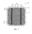
- the protruding electrodes 43 are described as, for example, unbroken linear lines. However, as shown in FIG. 7 , two or more protruding electrodes 43 may be aligned like broken lines with intervening spaces therebetween. Although, in the example shown in FIG. 7 , each of the protruding electrodes 43 has a rectangular shape which extends perpendicular to the broken line, the shape of the electrodes is not limited to this example. Each of the protruding electrodes 43 may have the shape of a string of dots or wavy edge lines with rough edges. Alternatively, as shown in FIG. 8 , the protruding electrodes 43 may be formed as zigzag lines. It should be noted that although various shapes are described as examples of the shape of protruding electrodes 43, the busbar electrode units 33 may have various shapes similarly to the protruding electrodes 43.
Landscapes
- Photovoltaic Devices (AREA)
- Life Sciences & Earth Sciences (AREA)
- Engineering & Computer Science (AREA)
- Sustainable Development (AREA)
- Sustainable Energy (AREA)
Abstract
Description
- The present invention relates to photoelectric converters and methods for producing the same.
- Patent Document 1 discloses a photoelectric converter which is provided with a photoelectric conversion unit, a light-receiving surface electrode provided on a light-receiving surface of the photoelectric conversion unit, and a rear surface electrode provided on the rear surface of the photoelectric conversion unit. In this photoelectric converter, each of the light-receiving surface electrode and the rear surface electrode is provided with two or more finger electrode units and two or more busbar electrode units connected to the finger electrode units.
-
- Patent Document 1:
JP 2009-290234 A - In photoelectric converters such as solar cells, transmittance of light in the infrared region may be problematic. As the photoelectric conversion units have come to have thinner layers, transmittance of light in other regions has also become problematic.
- However, when a metal layer such as a busbar electrode unit or the like is formed on a rear surface of a photoelectric converter, there is a risk of a defect energy level caused by metal atoms in the metal layer diffusing into a semiconductor layer of the photoelectric conversion unit. Such a defect energy level may lower photoelectric conversion efficiency of the photoelectric converter by trapping carriers which have been generated in the photoelectric conversion unit.
- A photoelectric converter according to the present invention includes a photoelectric conversion unit; a light-receiving surface electrode disposed on a light-receiving surface of the photoelectric conversion unit; and a rear surface electrode disposed on a rear surface of the photoelectric conversion unit; wherein the rear surface electrode comprises a transparent conductive film layered on the rear surface of the photoelectric conversion unit; and a metal film layered on substantially the entire surface of the transparent conductive film except for an edge area.
- A method for manufacturing a photoelectric converter according to the present invention includes preparing a photoelectric conversion unit; placing a mask covering at least apart of an edge area on a photoelectric conversion unit and layering a transparent conductive film on an area on the photoelectric conversion unit except for the edge area covered by the mask; and with the transparent conductive film attached to the mask, a metal film is layered on an area on the transparent conductive film. Alternatively, a method for manufacturing a photoelectric converter according to the present invention may include preparing a photoelectric conversion unit; placing a first mask covering at least a part of an edge area on a photoelectric conversion unit and layering a transparent conductive film on an area on the photoelectric conversion unit except for the edge area which is covered by the first mask; and placing a second mask covering at least a part of an edge area on the transparent conductive film and layering a metal film on an area on the transparent conductive film except for the edge area covered by the second mask.
- According to the present invention, a photoelectric converter having improved light conversion efficiency and a manufacturing method of the same are provided.
-
-
FIG. 1 shows a photoelectric converter according to an embodiment of the present invention viewed from a light-receiving surface side. -
FIG. 2 shows a photoelectric converter according to an embodiment of the present invention viewed from a rear surface side. -
FIG. 3 shows a schematic diagram of a cross-sectional view taken along the line B-B inFIGs. 1 and 2 . -
FIG. 4 shows a variation of a rear surface electrode. -
FIG. 5 shows a schematic diagram of part of a manufacturing process of a photoelectric converter according to an embodiment of the present invention. -
FIG. 6 shows a variation of a manufacturing process of a photoelectric converter according to an embodiment of the present invention. -
FIG. 7 shows a variation of a protruding electrode. -
FIG. 8 shows another variation of a protruding electrode. - A
photoelectric converter 10 according to an embodiment of the present invention and a method for manufacturing the same are described below by referring to the drawings. It should be noted that the embodiments shown below are provided merely as examples. The present invention is not limited to the embodiments shownbelow. Further, the drawings referred to in the embodiments are schematically illustrated, and thus the dimensional ratios or the like shown in the drawings may be different from the dimensional ratios of the actual elements. Dimensional ratios or the like of a specific element should be determined by referring to the description below. - First, a configuration of the
photoelectric converter 10 is described below by referring toFIGs. 1 to 4 . -
FIG. 1 shows thephotoelectric converter 10 viewed from a light-receiving surface side, whileFIG. 2 shows thephotoelectric converter 10 viewed from a rear surface side of thephotoelectric converter 10. As shown inFIGs. 1 and 2 , thephotoelectric converter 10 is provided with aphotoelectric conversion unit 20 and a light-receivingsurface electrode 30 provided on a light receiving surface of thephotoelectric conversion unit 20, and arear surface electrode 40 provided on a rear surface of thephotoelectric conversion unit 20. The "light-receiving surface" indicates a main incident surface of light from outside of the converter. For example, when assembling a module such as a solar cell including thephotoelectric converter 10, more than 50% to 100% of the incident light to the device comes from the light-receiving surface. The "rear surface" indicates a surface opposite the light-receiving surface. - The
photoelectric conversion unit 20 is a member to generate carriers (electrons and holes) by receiving light such as solar light. In thephotoelectric converter 10, the carriers generated by thephotoelectric conversion unit 20 are collected by the light-receivingsurface electrode 30 and therear surface electrode 40. The carriers are retrieved outside as electrical energy by assembling thephotoelectric converter 10 in a module by electrically connecting wiring members (not shown) to the light-receivingsurface electrode 30 and therear surface electrode 40. Thephotoelectric conversion unit 20 is provided with an n-type singlecrystalline silicon substrate 21 which is a crystalline semiconductor substrate having a substantially square shape. - As shown in
FIG. 1 , on the light-receiving surface of the n-type singlecrystalline silicon substrate 21, thephotoelectric conversion unit 20 is provided with a p-typeamorphous silicon film 23 layered via an i-typeamorphous silicon film 22. A transparentconductive film 31 included in the light-receivingsurface electrode 30 is layered on the light-receiving surface of the p-typeamorphous silicon film 23. Further,finger electrode units 32 andbusbar electrode units 33 for collecting electrical power generated by thephotoelectric conversion unit 20 are formed on the transparentconductive film 31. - As shown in
FIG. 2 , on the rear surface of the n-type singlecrystalline silicon substrate 21, thephotoelectric conversion unit 20 is provided with an n-typeamorphous silicon film 25 layered via an i-typeamorphous silicon film 24. A transparentconductive film 41 included in therear surface electrode 40 is layered on the rear surface of the n-type amorphous silicon film25. Further, ametal film 42 for collecting electrical power generated by thephotoelectric conversion unit 20 is formed on the transparentconductive film 41. Protrudingelectrodes 43 which are used as connecting units to the wire members are provided on themetal film 42. - In other words, the
photoelectric conversion unit 20 has a configuration in which amorphous semiconductor thin films are layered on both surfaces of a crystalline semiconductor substrate. Specifically, thephotoelectric conversion unit 20 has a layered configuration in which a p-typeamorphous silicon film 23, i-typeamorphous silicon film 22, n-type singlecrystal silicon substrate 21, i-typeamorphous silicon film 24, and n-typeamorphous silicon film 25 are layered in this order. In this layered configuration, the p-typeamorphous silicon film 23 side is the light-receiving surface side. - The configuration of the
photoelectric converter 10 is further described in detail below by referring toFIG. 3 (cross-sectional view taken along the line B-B inFIGs. 1 and 2 ) as appropriate, in addition toFIGs. 1 and 2 . - As shown in
FIG. 3 , thephotoelectric conversion unit 20 is provided with the i-typeamorphous silicon film 22 layered on the entire light-receiving surface of the n-type singlecrystal silicon substrate 21 and the i-typeamorphous silicon film 24 layered on the entire rear surface of the n-type singlecrystal silicon substrate 21. It should be noted that the i-typeamorphous silicon films crystal silicon substrate 21 except for an edge area. The i-typeamorphous silicon films photoelectric conversion unit 20 is provided with the p-typeamorphous silicon film 23 layered on the entire light-receiving surface of the i-typeamorphous silicon film 22 and the n-typeamorphous silicon film 25 layered on the entire rear surface of the i-typeamorphous silicon film 24. - The light-receiving surface and the rear surface of the photoelectric conversion unit 20 (n-type single crystal silicon substrate 21) can be respectively formed as textured surfaces (not shown). The textured surface indicates an uneven surface which increases amount of light absorption by the
photoelectric conversion unit 20 by restricting surface reflection. A specific example of the textured surface is an uneven surface having a pyramid shape (such as square pyramid and truncated pyramid) which can be obtained by applying anisotropic etching on the light-receiving surface and the rear surface of the n-type singlecrystal silicon substrate 21 having a (100) surface. It should be noted that the thickness of the photoelectric conversion unit 20 (the length of the film in the layered direction) is, for example, several hundred µm, most of which is the thickness of the n-type singlecrystal silicon substrate 21. The thickness of the amorphous silicon film is, for example, from several nm to several tens of nm. The height of unevenness of the texture structure is, for example, several µm. Therefore, the texture surface is reflected to the light-receiving surface and the rear surface of the amorphous silicon film. - As shown in
FIGs. 1 and3 , the light-receivingsurface electrode 30 includes a transparentconductive film 31, two or morefinger electrode units 32, and two or morebusbar electrode units 33. Thefinger electrode units 32 and thebusbar electrode units 33 are electrically connected to each other, and both are formed on the transparentconductive film 31. That is, in the light-receivingsurface electrode 30, carriers transmitted from the p-type amorphous silicon film23 via the transparentconductive film 31 are collected by thefinger electrode units 32 and thebusbar electrode units 33. When thephotoelectric converter 10 is assembled in a module, the carriers collected by thebusbar electrode units 33 which are electrically connected with the wire member are retrieved outside. - The transparent
conductive film 31 may be a thin film (TCO film) including at least one of metal oxides having a polycrystalline structure, such as indium oxide (In2O3), zinc oxide (ZnO), tin oxide (SnO2), and titanium oxide (TiO2). The transparentconductive film 31 functions as a light transmissive electrode unit. In the transparentconductive film 31, a dopant such as tin (Sn), zinc (Zn), tungsten (W), antimony (Sb), titanium (Ti), aluminum (Al), cerium (Ce), and gallium (Ga) may be doped in the above metal oxides. The concentration of the dopant may be 0 to 20 wt%. The thickness of the transparentconductive film 31 may be, for example, 50 nm to 200 nm. It is preferable that the transparentconductive film 31 is layered on the entire surface region except for the edge area (hereinafter referred to as "edge area A1") on the light-receiving surface of the p-typeamorphous silicon film 23. It is preferable that the edge area A1 on which the transparentconductive film 31 is not layered is a surface region having a width of about 1 to 2 mm from the edge of the light-receiving surface of the p-typeamorphous silicon film 23, and provided annularly along the circumference of the light-receiving surface. - The
finger electrode units 32 and thebusbar electrode units 33 are thin line electrode units formed from conductive paste made from binder resin in which conductive particles such as silver (Ag) are dispersed. Thefinger electrode units 32 and thebusbar electrode units 33 are provided to collect electrical power generated by thephotoelectric conversion unit 20 via the transparentconductive film 31. Thefinger electrode units 32 may be, for example, strip-shaped metal layers formed on the light-receiving surface so as to evenly collect electrical power from the entirephotoelectric conversion unit 20. It is preferable that thefinger electrode units 32 are positioned parallel to each other with intervening spaces of a predetermined length (for example, width of 100 µm, and an intervening space of 2 mm). - The
busbar electrode units 33 are provided to further collect the electrical power collected by thefinger electrode units 32. Thebusbar electrode units 33 may be, for example, strip shaped metal layers formed on the light-receiving surface. Thebusbar electrode units 33 are positioned to intersect with thefinger electrode units 32 to which thebusbar electrode units 33 are electrically connected. Thebusbar electrode units 33 may be positioned, for example, parallel to each other with an intervening space of a predetermined length. It is preferable that thebusbar electrode units 33 are arranged to be fewer and wider than the finger electrode units 32 (for example, width of 1.5mm, two pieces). It should be noted that the shapes of thefinger electrode units 32 and thebusbar electrode units 33 are not limited to the above mentioned shapes but various shapes such as a zigzag shape are also applicable. - As shown in
FIGs. 2 and3 , therear surface electrode 40 includes the transparentconductive film 41, themetal film 42, and the two or moreprotruding electrodes 43. The protrudingelectrodes 43 are electrodes having a shape protruding in the direction of thickness of thephotoelectric conversion unit 20 on themetal film 42. When thephotoelectric converter 10 is assembled in a module, the wiring member is connected to the protrudingelectrodes 43. The protrudingelectrodes 43 may have a strip shape made from, for example, conductive paste on themetal film 42. For example, two protrudingelectrodes 43 may be positioned parallel to each other with an intervening space of a predetermined length in the same direction as thebusbar electrode units 33. It should be noted that the shape of the protrudingelectrodes 43 is not limited to the above mentioned shape but various shapes such as a dot shape and zigzag shape are also applicable (refer toFIGs. 7 and8 described below). - Similarly to the transparent
conductive film 31, the transparentconductive film 41 may be formed from ITO, ZnO, SnO2, or the like, and function as a light transmissive electrode unit. Further, as described in detail below, the transparentconductive film 41 prevents direct contact between thephotoelectric conversion unit 20 and themetal film 42 and functions to raise the reflection ratio by interacting with themetal film 42. It is preferable that the transparentconductive film 41 has a thickness of about 50 nm to 200 nm and that the previously described texture surface is also applied to the rear surface of the transparentconductive film 41. - It is preferable that the transparent
conductive film 41 is layered on the entire surface region except for the edge area (hereinafter referred to as "edge area A2") on the rear surface of the n-typeamorphous silicon film 25. It is further preferable that the edge area A2 on which the transparentconductive film 41 is not layered is a surface region having a width of about 1 to 2 mm from the edge of the rear surface of the n-typeamorphous silicon film 25, and provided annularly along the circumference of the rear surface. - The
metal film 42 is a thin film made from a metal material having a high light reflection ratio and a high conductivity. Themetal film 42 preferably has a high reflection ratio for light in the infrared region. The reflection ratio of themetal film 42 is preferably higher than that of the transparentconductive film 41 at least for light in the infrared region. Themetal film 42 functions as an electrode which collects carriers transmitted from the n-typeamorphous silicon film 25 via the transparentconductive film 41. Themetal film 42 further has a function to reflect, to the light-receiving surface side, transmitted light which has passed through thephotoelectric conversion unit 20. Themetal film 42 is preferably thick enough to prevent light from passing through and thin enough to reflect the texture surface to the rear surface. For example, themetal film 42 preferably has a thickness of about 0.1 µm to 5 µm. By allowing the texture surface to also be reflected on the rear surface of themetal film 42, another advantage can be achieved that the contact between themetal film 42 and the protrudingelectrodes 43 becomes tighter. - Applicable metal material for the
metal film 42 is a metal, for example, silver (Ag), aluminum (A1), titan (Ti), rhodium (Rh), copper (Cu), gold (Au), platinum (Pt), nickel (Ni), chrome (Cr), or an alloy including at least one of these metals. It is preferable that the metal material has a high reflective ratio to light in the infrared region, in particular, a wavelength of about 800 nm to 1200 nm. Among the above listed materials, Ag, Al, Ti, Rh, Cu, and Au, and an alloy including at least one of these materials, are preferable. Materials, Ag, Al, and Ti and an alloy including at least one of these materials are more preferable, and Ag and an alloy including Ag are particularly preferable. - The
metal film 42 may be formed by two or more layered films made from the above metal materials. A layered body of AG film and Al film may be regarded as an example. In this case, the Ag film is preferably positioned on the transparentconductive film 41 side. An Ag-Al-Ag layered body in which both sides of the Al film are layered by Ag films, or, for example, an Ag-Cu-Ag layered body in which another metal film (such as Cu film) is used in place of the Al film may be used. - The
metal film 42 may be layered on substantially the entire surface of the transparentconductive film 41 except for an edge area (hereinafter referred to as "edge area A3"). It is more preferable that themetal film 42 may be layered on the entire surface of the transparentconductive film 41 except for the edge area A3. It should be noted that "being layered on substantially the entire surface of the transparentconductive film 41 except for an edge area" includes a state where themetal film 42 can be recognized to be layered on substantially the entire surface of the transparentconductive film 41, which includes a case in which a part of themetal film 42 layered on the transparentconductive film 41 is missing. Specifically, a state where themetal film 42 covers more than 95% of the transparentconductive film 41 except for the edge area A3 can be raised as an example. - The
metal film 42 is layered in at least part of the edge area A3 of the transparentconductive film 41 such that themetal film 42 does not cover the n-typeamorphous silicon film 25 across the transparentconductive film 41. In other words, themetal film 42 may be layered on a part of the edge area A3. However, it is preferable that themetal film 42 is layered so as not to cover the n-typeamorphous silicon film 25 beyond the transparentconductive film 41 on the entire circumference of the edge region A3 of the transparentconductive film 41. That is, it is preferable that, on the rear surface of the transparentconductive film 41, themetal film 42 is layered on the entire surface or substantially the entire surface except for the edge area A3. - The edge area A3 on which the
metal film 42 is not layered is preferably narrow in consideration of reflection or the like of transmissive light. For example, it is preferable that the edge area A3 has a width of 1 mm to 5 mm from the edge of the transparentconductive film 41. The edge area A3 is preferably provided annularly along the circumference of the rear surface of the transparentconductive film 41. The width of the edge area A3 can be checked by cross-sectional observation using a scanning electron microscope (SEM) or transmission electron microscope (TEM) (an optical microscope can also be used with a wide width). - When the
metal film 42 comes into contact with the edge area A2 of the n-typeamorphous silicon film 25 beyond at least a part of the edge area A3 of the transparentconductive film 41, an issue of carrier trap may occur because the metal atoms of themetal film 42 may diffuse into the n-typeamorphous silicon film 25 in that region to cause a defect energy level. However, because themetal film 42 is provided so as not to directly contact the rear surface of the photoelectric conversion unit 20 (n-type amorphous silicon film 25) via the transparentconductive film 41, it is possible to restrict occurrence of the defect energy level. It is preferable that the edge area A3 is provided annually along the entire circumference of the transparentconductive film 41 to avoid contact between themetal film 42 and the photoelectric conversion unit 20 (n-type amorphous silicon film 25) in the entire circumference of thephotoelectric conversion unit 20. This results in restriction of the occurrence of the defect energy level. - When the
photoelectric conversion unit 20 is configured to include an amorphous silicon film layered on a single crystal silicon substrate, the effect of the defect energy level caused by metals diffused into the amorphous silicon film increases. In such a case, an achievable advantage by preventing contact between thephotoelectric conversion unit 20 and themetal film 42 becomes significant. - The
metal film 42 is layered over a wide area of the rear surface of the photoelectric conversion unit 20 (n-type amorphous silicon film 25). In this way, the transmitted light that has entered from the light-receiving surface and passed through thephotoelectric conversion unit 20 can be reflected to the light-receiving surface by themetal film 42. Therefore, the light absorption ratio at thephotoelectric conversion unit 20 can be improved. - The
metal film 42 is layered on thephotoelectric conversion unit 20 via the transparentconductive film 41. In this way, the reflection ratio of themetal film 42 increases because light absorption is restricted by the occurrence of evanescent light. It should be noted that a texture surface is also applied on the rear surface of thephotoelectric conversion unit 20. Therefore, light scatters on the rear surface making it easier for thephotoelectric conversion unit 20 to capture light. - The transparent
conductive film 41 has high adhesive properties with both of thephotoelectric conversion unit 20 and themetal film 42. Therefore, it becomes possible to increase the adhesive strength (also known as peel strength) of themetal film 42. - Because of the above mentioned arrangements, light conversion efficiency can be improved by the
photoelectric converter 10 according to the present embodiment. - As shown in
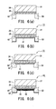
FIG. 4 , at least a part of side surface of themetal film 42 may be covered by the transparentconductive film 41. In other words, the transparentconductive film 41 has a protruding portion which covers a side surface of themetal film 42 in the edge area A2. The "side surface" of themetal film 42 indicates a surface along the thickness of themetal film 42. The shape having the protruding portion can be obtained by, for example, a method inFIG. 5 described below. The protruding portion has a width of about several nm to several hundred nm and a height (the length in the direction of thickness) of about the same as themetal film 42. In such a configuration, the same effects as mentioned above can be achieved. - Next, a method for manufacturing the
photoelectric converter 10 having the above configuration is described below. - With a clean n-type single
crystal silicon substrate 21 provided in a vacuum chamber, the i-typeamorphous silicon film 24 is layered on the substrate by, for example, plasma-enhanced chemical vapor deposition (plasma CVD). Next, n-typeamorphous silicon film 25 is layered on the i-typeamorphous silicon film 24. It should be noted that in the present embodiment, the surface of the n-type singlecrystal silicon substrate 21 on which the n-typeamorphous silicon film 25 is layered is the rear surface. In the layering process of the i-typeamorphous silicon film 24, for example, silane gas (SiH4) is used as source gas. In the layering process of the n-typeamorphous silicon film 25, for example, silane gas (SiH4), hydrogen (H2), or phosphine (PH3) is used as source gas. In this way, the i-typeamorphous silicon film 24 and the n-typeamorphous silicon film 25 are layered in this order on the rear surface of the n-type singlecrystal silicon substrate 21. - The i-type
amorphous silicon film 22 and the p-typeamorphous silicon film 23 can also be layered on the light receiving surface of the n-type singlecrystal silicon substrate 21 by the plasma CVD method. In the layering process of thep-typeamorphous silicon film 23, diborane (B2H6) is used as the source gas in place of PH3. Thefinger electrode units 32 and thebusbar electrode units 33 of the light-receivingsurface electrode 30 can be formed by, for example, screen printing conductive paste in a desired pattern on the transparentconductive film 31. Alternatively, instead of the screen printing method, various method such as sputtering methods, evaporation methods, and plating methods may be applied. It should be noted that the transparentconductive film 31 can be layered by the same method for the transparent conductive film 41 (as described below). - By referring to
FIG. 5 , the process to manufacture therear surface electrode 40, in particular, the layering process of the transparentconductive film 41 and themetal film 42 is described in detail below. InFIG. 5 , a layer configuration of the n-type singlecrystal silicon substrate 21 on the light-receiving surface side is omitted. The film layered on themask 50 is distinguished from the film layered on the rear surface of the n-type amorphous silicon film25byassigning "M" at the end of the reference numerals. -
FIG. 5 (a) indicates a state in which themask 50 is disposed on the rear surface of the n-typeamorphous silicon film 25. Themask 50 is disposed to cover the edge area A2 on the rear surface of the n-typeamorphous silicon film 25. Then, the transparentconductive film 41 is layered by, for example, a sputtering method on the rear surface of the n-typeamorphous silicon film 25 on which themask 50 has been disposed. As themask 50, for example, a metal support frame which supports the n-type singlecrystal silicon substrate 21 from the rear surface may be used. -
FIG. 5(b) shows anintermediate body 11 in which the transparentconductive film 41 is layered on the entire surface of the n-typeamorphous silicon film 25 except for the edge area A2. When the transparentconductive film 41 has been layered, the transparentconductive film 41M is also attached to themask 50. Specifically, the transparentconductive film 41M is attached not only on thesurface 51 of themask 50, but also on aside surface 52 of an opening. The transparentconductive film 41M attached to theside surface 52 of the opening has a thickness of, for example, about several nm to several hundred nm and is formed continuously with the transparentconductive film 41. Then, in a state in which themask 50 with the transparentconductive film 41 attached is disposed, themetal film 42 is layered on the rear surface of the transparentconductive film 41 by, for example, a sputtering method. -
FIG. 5(c) shows anintermediate body 12 in which themetal film 42 is layered on the entire rear surface of the transparentconductive film 41 except for the edge area A3. When themetal film 42 has been layered, themetal film 42M is also layered on the transparentconductive film 41M which is attached to thesurface 51 and theside surface 52 of the opening. In other words, when themetal film 42 is layered, because the transparentconductive film 41M is attached to theside surface 52 of the opening, themetal film 42 is layered to the surface which is narrower by the thickness of the transparentconductive film 41M than the entire surface of the opening of themask 50. That is, the transparentconductive film 41M attached to theside surface 52 of the opening functions as a mask to cover the edge area A3. - When the
mask 50 is removed after themetal film 42 has been layered, the transparentconductive film 41 and themetal film 42 of therear surface electrode 40 shown inFIG. 3 can be obtained. The transparentconductive film 41M and themetal film 42M attached to themask 50 are removed together with themask 50. As shown inFIG. 4 , a part of the transparentconductive film 41M attached to theside surface 52 of the opening may be left as a protruding portion. - The protruding
electrodes 43 maybe formed on the rear surface of themetal film 42 by the same method as the busbar electrode units33 (forexample, screenprintingmethods, sputteringmethods, evaporation methods, and plating methods). Alternatively, the protrudingelectrodes 43 may be formed by layering two or more films made of metal or alloy. - Another example of a method for manufacturing the
photoelectric converter 10 is described below by referring toFIG. 6 . - In the example shown in
FIG. 6 , the layering process (a, b) of the transparentconductive film 41 is the same as the example shown inFIG. 5 , while the layering process (c, d) of themetal film 42 is different from the one shown inFIG. 5 . Specifically, in the layering process of the transparentconductive film 41, the transparentconductive film 41 is layered on the entire surface except for the edge area A2 by using themask 50. However, as shown inFIG. 6(c) , in the layering process of themetal film 42, asecond mask 53 which covers the edge area A3 on the rear surface of the transparentconductive film 41 is used in place of themask 50. - As shown in
FIG. 6(d) , themetal film 42 is layered on the rear surface of the transparentconductive film 41 on which thesecond mask 53 is disposed. In this way, themetal film 42 can be layered on the entire surface of the transparentconductive film 41 except for the edge area A3. According to the method shown inFIG. 6 as an example, the width of the edge area A3 can be freely adjusted by changing the size of the opening of thesecond mask 53. - According to the present embodiment, designs can be arranged within a scope in which the object of the present invention can be achieved. For example, although the present embodiment describes, as an example, the
photoelectric conversion unit 20 having a configuration in which amorphous silicon films are layered on both surfaces of the n-type singlecrystal silicon substrate 21, the configuration of the photoelectric conversion unit is not limited to this example. The photoelectric conversion unit may be configured to include no i-typeamorphous silicon film 24 or n-typeamorphous silicon film 25, or to include a semiconductor other than silicon (such as gallium arsenide). Further, although the p-typeamorphous silicon film 23 side is assumed to be the light receiving surface side in the present embodiment, it is also possible to assume the n-typeamorphous silicon film 25 side as the light-receiving side by providing the light-receivingsurface electrode 30 on the n-typeamorphous silicon film 25. Furthermore, although in the present embodiment the light-receivingsurface electrode 30 and therear surface electrode 40 are described to respectively include thebusbar electrode units 33 and the protrudingelectrodes 43, the light-receivingsurface electrode 30 or therear surface electrode 40 may be so called busbarless electrodes having nobusbar electrode units 33 or protrudingelectrodes 43. - In the present embodiment, the protruding
electrodes 43 are described as, for example, unbroken linear lines. However, as shown inFIG. 7 , two or moreprotruding electrodes 43 may be aligned like broken lines with intervening spaces therebetween. Although, in the example shown inFIG. 7 , each of the protrudingelectrodes 43 has a rectangular shape which extends perpendicular to the broken line, the shape of the electrodes is not limited to this example. Each of the protrudingelectrodes 43 may have the shape of a string of dots or wavy edge lines with rough edges. Alternatively, as shown inFIG. 8 , the protrudingelectrodes 43 may be formed as zigzag lines. It should be noted that although various shapes are described as examples of the shape of protrudingelectrodes 43, thebusbar electrode units 33 may have various shapes similarly to the protrudingelectrodes 43. - 10 photoelectric converter, 11, 12 intermediate body, 20 photoelectric conversion unit, 21 n-type single crystal silicon substrate, 22, 24 i-type amorphous silicon film, 23 p-type amorphous silicon film, 25 n-type amorphous silicon film, 30 light-receiving surface electrode, 31, 41 transparent conductive film, 32 finger electrode unit, 33 busbar electrode unit, 40 rear surface electrode, 42 metal film, 43 protruding electrode, 50 mask, 51 surface, 52 side surface of opening, and 53 second mask.
Claims (8)
- A photoelectric converter comprising:a photoelectric conversion unit;a light-receiving surface electrode disposed on a light-receiving surface of the photoelectric conversion unit; anda rear surface electrode disposed on a rear surface of the photoelectric conversion unit;wherein the rear surface electrode comprises
a transparent conductive film layered on the rear surface of the photoelectric conversion unit; and
a metal film layered on substantially the entire surface of the transparent conductive film except for an edge area. - The photoelectric converter according to claim 1, wherein
the metal film is layered on the entire surface of the transparent conductive film except for the edge area. - The photoelectric converter according to claim 1 or 2, wherein
none of the metal film is layered on the entire circumference of the edge area on the transparent conductive film. - The photoelectric converter according to any one of claims 1 to 3, wherein
a reflection ratio of the metal film is higher than that of the transparent conductive film at least for light in an infrared region. - The photoelectric converter according to any one of claims 1 to 3, wherein
the metal film includes at least Ag. - The photoelectric converter according to any one of claims 1 to 5, wherein
the photoelectric conversion unit comprises:a crystalline semiconductor substrate; andan amorphous semiconductor film layered on a rear surface of the crystalline semiconductor substrate,wherein the transparent conductive film is layered on a rear surface of the amorphous semiconductor film. - A method for manufacturing a photoelectric converter comprising:providing a photoelectric conversion unit;placing a mask covering at least a part of an edge area on the photoelectric conversion unit and layering a transparent conductive film on an area on the photoelectric conversion unit except for the edge area covered by the mask; andwith the transparent conductive film attached to the mask, layering a metal film on an area on the transparent conductive film.
- A method for manufacturing a photoelectric converter comprising:providing a photoelectric conversion unit;placing a first mask covering at least a part of an edge area on the photoelectric conversion unit and layering a transparent conductive film on an area on the photoelectric conversion unit except for the edge area which is covered by the first mask; andplacing a second mask covering at least a part of an edge area on the transparent conductive film and layering a metal film on an area on the transparent conductive film except for the edge area covered by the second mask.
Applications Claiming Priority (2)
| Application Number | Priority Date | Filing Date | Title |
|---|---|---|---|
| JP2011018320 | 2011-01-31 | ||
| PCT/JP2011/080521 WO2012105155A1 (en) | 2011-01-31 | 2011-12-28 | Photoelectric converter and method for producing same |
Publications (2)
| Publication Number | Publication Date |
|---|---|
| EP2657978A1 true EP2657978A1 (en) | 2013-10-30 |
| EP2657978A4 EP2657978A4 (en) | 2014-03-19 |
Family
ID=46602385
Family Applications (1)
| Application Number | Title | Priority Date | Filing Date |
|---|---|---|---|
| EP11857851.7A Withdrawn EP2657978A4 (en) | 2011-01-31 | 2011-12-28 | PHOTOELECTRIC CONVERTER AND METHOD OF MANUFACTURING THE SAME |
Country Status (5)
| Country | Link |
|---|---|
| US (1) | US20140130857A1 (en) |
| EP (1) | EP2657978A4 (en) |
| JP (1) | JPWO2012105155A1 (en) |
| CN (1) | CN103339734A (en) |
| WO (1) | WO2012105155A1 (en) |
Cited By (2)
| Publication number | Priority date | Publication date | Assignee | Title |
|---|---|---|---|---|
| EP3196945A1 (en) * | 2016-01-20 | 2017-07-26 | Lg Electronics Inc. | Solar cell |
| US12295179B2 (en) | 2020-07-22 | 2025-05-06 | Canon Kabushiki Kaisha | Light detecting element and photoelectric conversion device |
Families Citing this family (12)
| Publication number | Priority date | Publication date | Assignee | Title |
|---|---|---|---|---|
| JP5843734B2 (en) * | 2012-09-10 | 2016-01-13 | 三菱電機株式会社 | Photoelectric conversion element and manufacturing method thereof |
| JPWO2015045263A1 (en) * | 2013-09-26 | 2017-03-09 | パナソニックIpマネジメント株式会社 | Solar cell and solar cell module |
| TWI469380B (en) * | 2013-11-08 | 2015-01-11 | Ind Tech Res Inst | Heterojunction solar cell structure |
| WO2015145944A1 (en) * | 2014-03-25 | 2015-10-01 | パナソニックIpマネジメント株式会社 | Photoelectric conversion element and photoelectric conversion element manufacturing method |
| JP6650407B2 (en) * | 2014-09-30 | 2020-02-19 | 株式会社カネカ | Method of manufacturing solar cell and method of manufacturing solar cell module |
| JP6000315B2 (en) * | 2014-10-15 | 2016-09-28 | 長州産業株式会社 | Photovoltaic element manufacturing method |
| WO2016157979A1 (en) * | 2015-03-31 | 2016-10-06 | 株式会社カネカ | Photoelectric conversion device and photoelectric conversion module |
| JP7454357B2 (en) * | 2019-11-01 | 2024-03-22 | 株式会社カネカ | Mask tray and solar cell manufacturing method |
| JP7677033B2 (en) * | 2021-07-28 | 2025-05-15 | 株式会社リコー | Photoelectric conversion element, electronic device, and power supply module |
| TWI777786B (en) * | 2021-09-27 | 2022-09-11 | 凌巨科技股份有限公司 | Solar cell with transparent type |
| JPWO2024157590A1 (en) * | 2023-01-26 | 2024-08-02 | ||
| CN118053924A (en) * | 2024-02-06 | 2024-05-17 | 浙江晶科能源有限公司 | Solar cell and preparation method thereof, laminated cell and photovoltaic module |
Family Cites Families (15)
| Publication number | Priority date | Publication date | Assignee | Title |
|---|---|---|---|---|
| JPS6041878B2 (en) * | 1979-02-14 | 1985-09-19 | シャープ株式会社 | Thin film solar cell |
| JPS5854678A (en) * | 1981-09-28 | 1983-03-31 | Hitachi Ltd | solar cell element |
| JP3244369B2 (en) * | 1993-11-19 | 2002-01-07 | 三洋電機株式会社 | Photovoltaic device with heterojunction |
| EP0734075B1 (en) * | 1994-10-06 | 2009-06-17 | Kanegafuchi Kagaku Kogyo Kabushiki Kaisha | Thin film solar cell |
| JP3349308B2 (en) * | 1995-10-26 | 2002-11-25 | 三洋電機株式会社 | Photovoltaic element |
| JP3469729B2 (en) * | 1996-10-31 | 2003-11-25 | 三洋電機株式会社 | Solar cell element |
| AU6420398A (en) * | 1997-03-21 | 1998-10-20 | Sanyo Electric Co., Ltd. | Photovoltaic element and method for manufacture thereof |
| JP2000150934A (en) * | 1998-11-16 | 2000-05-30 | Sanyo Electric Co Ltd | Photovoltaic device and method for manufacturing the same |
| NL1010635C2 (en) * | 1998-11-23 | 2000-05-24 | Stichting Energie | A method of manufacturing a metallization pattern on a photovoltaic cell. |
| JP2002141534A (en) * | 2000-11-02 | 2002-05-17 | Sharp Corp | Electrode of semiconductor substrate and method of manufacturing the same |
| JP4194379B2 (en) * | 2003-01-22 | 2008-12-10 | 三洋電機株式会社 | Photovoltaic device |
| JP2004296550A (en) * | 2003-03-25 | 2004-10-21 | Sanyo Electric Co Ltd | Photovoltaic element and its fabricating process |
| CN100431177C (en) * | 2003-09-24 | 2008-11-05 | 三洋电机株式会社 | Photovoltaic element and manufacturing method thereof |
| JP4222991B2 (en) * | 2004-01-13 | 2009-02-12 | 三洋電機株式会社 | Photovoltaic device |
| JP5031007B2 (en) | 2009-09-07 | 2012-09-19 | 三洋電機株式会社 | Photovoltaic element |
-
2011
- 2011-12-28 CN CN2011800664651A patent/CN103339734A/en active Pending
- 2011-12-28 EP EP11857851.7A patent/EP2657978A4/en not_active Withdrawn
- 2011-12-28 JP JP2012555713A patent/JPWO2012105155A1/en active Pending
- 2011-12-28 WO PCT/JP2011/080521 patent/WO2012105155A1/en not_active Ceased
-
2013
- 2013-07-29 US US13/953,052 patent/US20140130857A1/en not_active Abandoned
Cited By (3)
| Publication number | Priority date | Publication date | Assignee | Title |
|---|---|---|---|---|
| EP3196945A1 (en) * | 2016-01-20 | 2017-07-26 | Lg Electronics Inc. | Solar cell |
| EP3544059A1 (en) * | 2016-01-20 | 2019-09-25 | Lg Electronics Inc. | Solar cell |
| US12295179B2 (en) | 2020-07-22 | 2025-05-06 | Canon Kabushiki Kaisha | Light detecting element and photoelectric conversion device |
Also Published As
| Publication number | Publication date |
|---|---|
| JPWO2012105155A1 (en) | 2014-07-03 |
| CN103339734A (en) | 2013-10-02 |
| EP2657978A4 (en) | 2014-03-19 |
| WO2012105155A1 (en) | 2012-08-09 |
| US20140130857A1 (en) | 2014-05-15 |
Similar Documents
| Publication | Publication Date | Title |
|---|---|---|
| US20140130857A1 (en) | Photoelectric converter and method for producing same | |
| US20150090317A1 (en) | Solar cell, solar cell module, and method for producing solar cell | |
| US20200203540A1 (en) | Solar cell and electronic device provided with said solar cell | |
| US20130312826A1 (en) | Photovoltaic device and photovoltaic module | |
| JP6677801B2 (en) | Crystalline silicon-based solar cell, method of manufacturing the same, and solar cell module | |
| US9184320B2 (en) | Photoelectric conversion device | |
| EP2672522A1 (en) | Photoelectric conversion element | |
| JPWO2017078164A1 (en) | Method for manufacturing crystalline silicon-based solar cell and method for manufacturing crystalline silicon-based solar cell module | |
| KR20150090606A (en) | Solar cell and manufacturing method thereof | |
| US20150228817A1 (en) | Solar cell | |
| US20160322522A1 (en) | Solar cell | |
| CN110870081A (en) | Solar cells and solar cell modules | |
| US20190305151A1 (en) | Solar cell and manufacturing method of the same | |
| JP7270598B2 (en) | Solar cell and electronic device equipped with the solar cell | |
| JP7270597B2 (en) | Solar cell and electronic device equipped with the solar cell | |
| WO2012105153A1 (en) | Photoelectric conversion element | |
| JPWO2015045263A1 (en) | Solar cell and solar cell module | |
| EP2738819A1 (en) | Solar cell | |
| KR101173626B1 (en) | Solar cell | |
| WO2012105154A1 (en) | Method for manufacturing photoelectric conversion element | |
| KR20120135995A (en) | A solar cell and a manufacturing method thereof | |
| KR20130036887A (en) | Photovoltaic device | |
| EP3067940B1 (en) | Solar cell | |
| CN118571960A (en) | Solar cell modules and solar cell systems | |
| CN118738184A (en) | An intermediate zone solar cell and its manufacturing method and photovoltaic module |
Legal Events
| Date | Code | Title | Description |
|---|---|---|---|
| PUAI | Public reference made under article 153(3) epc to a published international application that has entered the european phase |
Free format text: ORIGINAL CODE: 0009012 |
|
| 17P | Request for examination filed |
Effective date: 20130723 |
|
| AK | Designated contracting states |
Kind code of ref document: A1 Designated state(s): AL AT BE BG CH CY CZ DE DK EE ES FI FR GB GR HR HU IE IS IT LI LT LU LV MC MK MT NL NO PL PT RO RS SE SI SK SM TR |
|
| A4 | Supplementary search report drawn up and despatched |
Effective date: 20140217 |
|
| RIC1 | Information provided on ipc code assigned before grant |
Ipc: H01L 31/18 20060101ALI20140211BHEP Ipc: H01L 31/0224 20060101AFI20140211BHEP Ipc: H01L 31/0747 20120101ALI20140211BHEP |
|
| DAX | Request for extension of the european patent (deleted) | ||
| 17Q | First examination report despatched |
Effective date: 20150210 |
|
| RAP1 | Party data changed (applicant data changed or rights of an application transferred) |
Owner name: PANASONIC INTELLECTUAL PROPERTY MANAGEMENT CO., LT |
|
| STAA | Information on the status of an ep patent application or granted ep patent |
Free format text: STATUS: THE APPLICATION IS DEEMED TO BE WITHDRAWN |
|
| 18D | Application deemed to be withdrawn |
Effective date: 20160701 |