EP2653975B1 - Sensormodul - Google Patents
Sensormodul Download PDFInfo
- Publication number
- EP2653975B1 EP2653975B1 EP13001431.9A EP13001431A EP2653975B1 EP 2653975 B1 EP2653975 B1 EP 2653975B1 EP 13001431 A EP13001431 A EP 13001431A EP 2653975 B1 EP2653975 B1 EP 2653975B1
- Authority
- EP
- European Patent Office
- Prior art keywords
- signal
- sensor
- processing device
- sensor module
- signal processing
- Prior art date
- Legal status (The legal status is an assumption and is not a legal conclusion. Google has not performed a legal analysis and makes no representation as to the accuracy of the status listed.)
- Active
Links
Images
Classifications
-
- G—PHYSICS
- G01—MEASURING; TESTING
- G01D—MEASURING NOT SPECIALLY ADAPTED FOR A SPECIFIC VARIABLE; ARRANGEMENTS FOR MEASURING TWO OR MORE VARIABLES NOT COVERED IN A SINGLE OTHER SUBCLASS; TARIFF METERING APPARATUS; MEASURING OR TESTING NOT OTHERWISE PROVIDED FOR
- G01D21/00—Measuring or testing not otherwise provided for
-
- G—PHYSICS
- G06—COMPUTING; CALCULATING OR COUNTING
- G06F—ELECTRIC DIGITAL DATA PROCESSING
- G06F13/00—Interconnection of, or transfer of information or other signals between, memories, input/output devices or central processing units
- G06F13/38—Information transfer, e.g. on bus
- G06F13/40—Bus structure
- G06F13/4063—Device-to-bus coupling
- G06F13/4068—Electrical coupling
Definitions
- the invention relates to a sensor module having at least one sensor for detecting and converting a physical quantity into an electrical sensor signal, having an electrical interface, which is designed to provide the sensor signal to a processing device, wherein the electrical interface is assigned a signal processing device that can be switched over the sensor signal is formed at an interface contact of the interface optionally as a positive binary voltage signal PNP or as a negative binary voltage signal NPN and / or is designed to switchable provision of the sensor signal at an interface contact of the interface either as an analog voltage signal or as an analog current signal.
- Such sensor modules are used in particular in fluid controls for detecting fluid-related measured values such as pressure, temperature, volume flow, flow velocity, etc.
- the DE 102006054421 A1 discloses a device with at least one sensor for detecting at least one process variable and with at least one modular transducer circuit, which has at least one sensor unit which uses the process variable detected by the sensor to be a measured variable determines and supplies the sensor with the necessary energy, and at least one application-specific signal processing unit for determining a measured value from the measured variable, wherein between the sensor unit and the signal processing unit, a conditioned output signal is provided, wherein the signal processing unit is designed interchangeable and wherein, depending on a predetermined measurement accuracy with which the device determines the measured value, several different types of signal processing units are provided.
- a control circuit for configuring at least one I / O module connector pin comprising at least one terminal which controls a configuration of the at least one pin, and wherein the at least one terminal is a pull-down terminal and / or a pull-up terminal and / or a discrete high terminal and / or a discrete low terminal and / or a positive 15 volt terminal and / or a negative 15 volt terminal and / or an area terminal and or a voltage output terminal.
- a sensor signal at the I / O module connector pin can be provided as a voltage signal in different forms.
- a multiplicity of applications with the same drive circuit for the electrical interface can already be satisfactorily controlled.
- the object of the invention is to provide a sensor module with which a considerable increase in the application bandwidth can be achieved with little additional effort.
- the signal processing device is designed for an additional provision of the sensor signal at the respective interface contact in the form of a digital voltage signal.
- the signal processing device preferably comprises a corresponding digital module, which converts the sensor signal into a coding in accordance with a specifiable communication protocol or another digital coding and makes available at the interface contact.
- a corresponding digital module which converts the sensor signal into a coding in accordance with a specifiable communication protocol or another digital coding and makes available at the interface contact.
- the signal processing device for the switchable provision of the sensor signal is designed optionally as a positive binary voltage signal PNP, as a negative binary voltage signal NPN, as an analog voltage signal, as an analog current signal or as a digital voltage signal at the interface contact.
- PNP positive binary voltage signal
- NPN negative binary voltage signal
- an analog voltage signal as an analog current signal or as a digital voltage signal at the interface contact.
- the current signal at the electrical interface in a proportional relationship or in another predeterminable, in particular clear, relationship to a signal level of the sensor of the sensor device.
- the total number of necessary interface contacts can be limited with this measure, since a larger number of signal forms, in particular all commonly required signal forms, can be provided for the sensor signal at a single interface contact.
- the structure of the electronic circuit in the sensor module can be standardized, since no different circuit variants must be kept, with which the sensor module otherwise has to be equipped depending on the customer with respect to the provision of the output signal.
- the electrical interface of the sensor module comprises two supply connections and two or alternatively three output connections, of which at least one output connection can be controlled by the signal processing device in the manner according to the invention.
- the further output terminal may be configured as a current or voltage output in a predefined manner or, according to a second alternative, likewise be driven by the signal processing device in the manner according to the invention.
- the signal processing device is designed for an additional, optional provision of the sensor signal as a digital voltage signal according to the I / O link protocol at the interface.
- the sensor signal is designed for an additional, optional provision of the sensor signal as a digital voltage signal according to the I / O link protocol at the interface.
- the signal processing device for the optional provision of the sensor signal in different signal forms parallel to each other, electrically controllable driver stages.
- Each of the driver stages can be designed either as a discrete electronic component or as part of the signal processing device.
- the signal processing device is preferably designed as a microcontroller or microprocessor, in particular as a specifically adapted microchip (ASIC, application-specific integrated circuit) or as a field programmable logic gate array (FPGA, Field Programmable Gate Array).
- ASIC application-specific integrated circuit
- FPGA Field Programmable Gate Array
- Each of the driver stages serves to provide the sensor signal provided by the sensor on request by the signal processing device in the respective predefined manner, in particular as a voltage signal or current signal, to the electrical interface.
- At least one interface contact is assigned an I / O link driver stage and a parallel connection of a binary, negative voltage driver stage and a binary, positive voltage driver stage and / or a parallel circuit of an analog voltage driver stage and an analog current driver stage.
- the signal processing device comprises a compensation module for the compensation of leakage currents during operation of the current driver stage.
- the leakage currents are caused for example by the parallel connection of the driver stages and affect the accuracy of the current signal to be forwarded to the downstream processing device. For example, when a current signal is provided at the electrical interface, the effect occurs that a part of the supplied current flows off into the remaining driver stages and thus an undesired falsification of the current signal occurs.
- the compensation module serves to prevent this falsification of the current signal, at least largely, by providing an additional current flow which corresponds at least almost to the leakage currents.
- the compensation module can be designed as a discrete electronic component or as an integral part of the signal processing device.
- the compensation module is a program element of a program necessary for operating the signal processing device.
- the compensation module can be set up such that a current signal determined by the signal processing device as a function of the input signal of the sensor and provided for transmission to the current driver stage is changed by a predefinable amount to the desired one To cause leakage current compensation.
- the compensation module can be embodied as an independent current source which provides an additional current flow which at least substantially supplements the current flow of the current driver stage by the leakage currents.
- the compensation module is designed to provide a fixed or an adjustable compensation value for driving the current driver stage.
- the fixed compensation value can be used if the requirements for the accuracy of the current signal at the electrical interface are located in a central region or if it is ensured by the construction of the signal processing device and the driver stages that substantially the same leakage currents always occur in the case of a multiplicity of sensor modules occur.
- the adjustable compensation value is to be provided when high demands are to be made on the accuracy of the current signal provided at the electrical interface, or if the leakage of the leakage currents across a plurality of sensor modules is in a range which makes reasonable use of the sensor signal without excludes an individual calibration of the sensor modules.
- a subsequent calibration step can then optionally by setting a parameter of the program element formed as part of a program for operating the signal processing means compensation module or by adjustment or trimming an electrical or electronic component of the compensation module designed as a circuit component, the required correction for the current signal is made.
- an input device for selecting an operating mode for the signal processing device and / or an information output device for displaying a selected operating mode of the signal processing device are coupled to the signal processing device.
- a selection can be made by a user, in which way the sensor signal is provided at the electrical interface.
- the display device which may be a light source or a segment display or a freely programmable display, serves to indicate to the user the selection made and / or other information about the sensor module.
- the electrical interface as an array of plug contacts, preferably as a socket, in particular as M8 socket or as M12 socket formed.
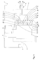
- An embodiment of a sensor module 1 shown schematically in the form of a block diagram in the figure as essential components a sensor 2, a signal processing device 3, an electrical interface 4, an input device 5 and an information output device 6.
- the sensor module 1 is provided for determining the amount of a physical quantity such as pressure, temperature, flow rate, flow rate, etc.
- the sensor 2 is designed such that it detects the physical quantity and outputs a dependent of the amount of the detected physical quantity of electrical sensor signal via a sensor line 7 to the signal processing device 3.
- the signal processing device 3 comprises, by way of example, a microcontroller 8 and a plurality of driver stages 9 to 11 and 13 to 16 connected downstream of the microcontroller 8.
- the driver stages 9, 10 and 11 are electrically connected in parallel with one another and form a first output stage 31.
- the driver stages 13 to 16 are likewise parallel connected to each other and form a second output stage 32.
- Each of the driver stages 9 to 11 and 13 to 16 is electrically connected by means of a signal line 25 and 26 to the microcontroller 8 and receives the prepared by the microcontroller 8 sensor signal.
- the two output stages 31 and 32 are each connected to an output terminal of the electrical interface 4 designed as an interface contact 18 or 19 and respectively provide the sensor signal there in a predeterminable manner.
- the electrical interface 4 has, by way of example, two interface contacts 20, 21 serving as supply terminals, to which a supply voltage for the sensor module 1 can be provided.
- the driver stage 9 is embodied as an I / O link driver stage by way of example and can be connected to a common node 22, the is electrically connected to the interface contact 18, provide a voltage signal in which the sensor signal is encoded according to the I / O link protocol.
- the driver stage 10 is exemplarily designed as a positive voltage driver stage and can provide a positive binary voltage signal PNP to the node 22.
- the driver stage 11 is embodied by way of example as a negative voltage driver stage and can provide a negative binary voltage signal NPN to the node 22.
- the driver stage 12 is designed as an example as an analog voltage driver stage and can provide an analog voltage signal corresponding to the sensor signal to the node 28.
- the driver stage 13 is configured by way of example as a positive voltage driver stage and can provide a positive binary voltage signal PNP to the node 28.
- the driver stage 14 is embodied by way of example as a negative voltage driver stage and can provide a negative binary voltage signal NPN to the node 28.
- the driver stage 15 is designed as an I / O link driver stage and the driver stage 16 as a current driver stage.
- Each of the driver stages 9 to 11 and 13 to 16 is in each case assigned an activation line 23 or 24 which makes it possible to provide an activation signal by the microcontroller 8 to the respective driver stage 9 to 11 and 13 to 16 to be activated.
- the driver stages 9 to 11 and 13 to 16 are set up such that they are permanently connected to the sensor signal processed by the microcontroller 8 be acted upon, but only then provide an output signal to the Koten Vietnamese 22 of the first output stage 31 and to the node 28 of the second output stage 32 when applied to the respectively associated activation line 23 and 24 to be provided by the microcontroller 8 activation signal.
- the current driver stage 16 is assigned, by way of example, a compensation module 29, which is designed by way of example for an additional provision of a current flow, which can be output by the current driver stage 16 to the node 28.
- the compensation module 29 is formed as a discrete component, which is preferably arranged on a common printed circuit with the microcontroller 8 and the driver stages 9 to 16.
- the compensation module 29 is controlled by the microcontroller 8 via a control line 30, wherein the control is preferably designed such that the current flow additionally provided by the compensation module 29 is dependent on a predefinable parameter or parameter field, which is stored in the microcontroller 8.
- the parameter or the parameter field in the manufacture of the sensor module 1 are determined in a calibration step and stored in the microcontroller 8.
- the compensation module is designed as a program element within a program for operating the signal processing device and can be transmitted in particular via the activation line to the Stromtreiberh to effect a correction of the voltage applied to the input of the Stromtreibercase, processed by the microcontroller sensor signal and thus a at least partially allow compensation of the leakage currents in the signal processing device 3.
Description
- Die Erfindung betrifft ein Sensormodul mit wenigstens einem Sensor zur Erfassung und Umwandlung einer physikalischen Größe in ein elektrisches Sensorsignal, mit einer elektrischen Schnittstelle, die zur Bereitstellung des Sensorsignals an eine Verarbeitungseinrichtung ausgebildet ist, wobei der elektrischen Schnittstelle eine Signalverarbeitungseinrichtung zugeordnet ist, die zur umschaltbaren Bereitstellung des Sensorsignals an einem Schnittstellenkontakt der Schnittstelle wahlweise als positives binäres Spannungssignal PNP oder als negatives binäres Spannungssignal NPN ausgebildet ist und/oder die zur umschaltbaren Bereitstellung des Sensorsignals an einem Schnittstellenkontakt der Schnittstelle wahlweise als analoges Spannungssignal oder als analoges Stromsignal ausgebildet ist.
- Derartige Sensormodule werden insbesondere in Fluidsteuerungen zur Erfassung von fluidbezogenen Messwerten wie Druck, Temperatur, Volumenstrom, Strömungsgeschwindigkeit, etc. eingesetzt.
- Die
DE 102006054421 A1 offenbart eine Vorrichtung mit zumindest einem Sensor zum Erfassen wenigstens einer Prozessgröße und mit zumindest einer modular aufgebauten Messwandlerschaltung, welcher zumindest eine Sensoreinheit, die aus der vom Sensor erfassten Prozessgröße eine Messgröße ermittelt und den Sensor mit der notwendigen Energie versorgt, und zumindest einer anwendungsspezifischen Signalverarbeitungseinheit zur Ermittlung eines Messwerts aus der Messgröße umfasst, wobei zwischen der Sensoreinheit und der Signalverarbeitungseinheit ein konditioniertes Ausgangssignal vorgesehen ist, wobei die Signalverarbeitungseinheit austauschbar ausgestaltet ist und wobei, in Abhängigkeit von einer vorgebbaren Messgenauigkeit, mit der die Vorrichtung den Messwert ermittelt, mehrere unterschiedliche Arten von Signalverarbeitungseinheiten vorgesehen sind. - Aus der
DE 102 31 950 A1 ist eine Steuerschaltung zur Konfiguration zumindest eines E/A-Modul-Steckerpins bekannt, wobei die Schaltung zumindest einen Anschluss umfasst, der eine Konfiguration des zumindest einen Pins steuert und wobei der zumindest eine Anschluss einen Pull-down-Anschluss und/oder einen Pull-up-Anschluss und/oder einen Diskret-hoch-Anschluss und/oder einen Diskretniedrig-Anschluss und/oder einen Positive-15-Volt-Anschluss und/oder einen Negative-15-Volt-Anschluss und/oder einen Bereichsanschluss und/oder einen Spannungsausgangsanschluss umfasst. - Damit kann gemäß dem Stand der Technik ein Sensorsignal am E/A-Modul-Steckerpin als Spannungssignal in unterschiedlichen Ausprägungen bereitgestellt werden. Durch diese unterschiedlichen Möglichkeiten zur Bereitstellung eines elektrischen Spannungssignals am Pin kann bereits eine Vielzahl von Anwendungsfällen mit der gleichen Ansteuerungsschaltung für die elektrische Schnittstelle zufriedenstellend beherrscht werden.
- Die Aufgabe der Erfindung besteht darin, ein Sensormodul bereitzustellen, mit dem mit geringem Zusatzaufwand eine erhebliche Vergrößerung der Anwendungsbandbreite erreicht werden kann.
- Diese Aufgabe wird für ein Sensormodul der eingangs genannten Art mit den Merkmalen des Anspruchs 1 gelöst. Hierbei ist vorgesehen, dass die Signalverarbeitungseinrichtung für eine zusätzliche Bereitstellung des Sensorsignals am jeweiligen Schnittstellenkontakt in Form eines digitalen Spannungssignals ausgebildet ist.
- Hierzu umfasst die Signalverarbeitungsvorrichtung vorzugsweise einen entsprechenden Digitalbaustein, der das Sensorsignal in eine Codierung gemäß einem vorgebbaren Kommunikationsprotokoll oder eine andere digitale Codierung wandelt und am Schnittstellenkontakt bereitstellt. Dadurch wird das Einsatzgebiet für das entsprechend ausgerüstete Sensormodul erheblich vergrößert.
- Vorteilhafte Weiterbildungen der Erfindung sind in den Unteransprüchen angegeben.
- Vorteilhaft ist es, wenn die Signalverarbeitungseinrichtung für die umschaltbare Bereitstellung des Sensorsignals wahlweise als positives binäres Spannungssignal PNP, als negatives binäres Spannungssignal NPN, als analoges Spannungssignal, als analoges Stromsignal oder als digitales Spannungssignal am Schnittstellenkontakt ausgebildet ist. Hierdurch wird die Vielseitigkeit für die Verwendung des Sensormoduls nochmals erheblich vergrößert und die Anzahl von unterschiedlichen Schaltungsaufbauten für das Sensormodul, die bislang notwendig war, um den Anforderungen nach unterschiedlich aufbereiteten Ausgangssignalen des Sensormoduls gerecht zu werden, kann reduziert, vorzugsweise auf einen einzigen Schaltungsaufbau beschränkt, werden.
- Dabei ist vorzugsweise vorgesehen, das Stromsignal an der elektrischen Schnittstelle in proportionaler Beziehung oder in einer anderen vorgebbaren, insbesondere eindeutigen, Beziehung zu einem Signalpegel des Sensors der Sensoreinrichtung bereitzustellen. Durch die Verwendung eines Stromsignals kann auch bei ungünstigen elektrischen Randbedingungen, beispielsweise bei langen elektrischen Leitungsverbindungen zwischen dem Sensormodul und einer nachgeschalteten Verarbeitungseinrichtung, eine zuverlässige Signalübertragung sichergestellt werden. Im Gegensatz zu den analogen oder digitalen Spannungssignalen, bei denen der Signalverarbeitungseinrichtung keine Informationen darüber zur Verfügung stehen, welcher Signalpegel tatsächlich an der nachgeschalteten Verarbeitungseinrichtung ankommt, ist bei einer Bereitstellung des Sensorsignals als Stromsignal bei Einhaltung gewisser elektrischer Mindestanforderungen für die Weiterleitung des Stromsignals an die Verarbeitungseinrichtung eine zuverlässigere Signalübertragung möglich.
- Zudem kann mit dieser Maßnahme die Gesamtanzahl der notwendigen Schnittstellenkontakte beschränkt werden, da an einem einzigen Schnittstellenkontakt eine größere Vielzahl von Signalformen, insbesondere alle üblicherweise geforderten Signalformen, für das Sensorsignal bereitgestellt werden können. Zudem kann hierdurch der Aufbau der elektronischen Schaltung im Sensormodul vereinheitlicht werden, da keine unterschiedlichen Schaltungsvarianten bereitgehalten werden müssen, mit denen das Sensormodul ansonsten je nach Kundenwunsch bezüglich der Bereitstellung des Ausgangssignals ausgerüstet werden muss. Typischerweise umfasst die elektrische Schnittstelle des Sensormoduls zwei Versorgungsanschlüsse sowie zwei oder alternativ drei Ausgangsanschlüsse, von denen zumindest ein Ausgangsanschluss von der Signalverarbeitungseinrichtung in der erfindungsgemäßen Weise angesteuert werden kann. Der weitere Ausgangsanschluss kann gemäß einer ersten Alternative in fest vorgegebener Weise als Strom- oder Spannungsausgang konfiguriert sein oder gemäß einer zweiten Alternative ebenfalls von der Signalverarbeitungseinrichtung in der erfindungsgemäßen Weise angesteuert werden.
- Vorteilhaft ist es, wenn die Signalverarbeitungseinrichtung für eine zusätzliche, wahlweise Bereitstellung des Sensorsignals als digitales Spannungssignal gemäß dem I/O-Link-Protokoll an der Schnittstelle ausgebildet ist. Hierdurch kann mit einem geringen schaltungstechnischen Aufwand eine zuverlässige Signalübertragung und ein auf unterschiedliche Einsatzbedingungen anpassbare Signalausgabe des Sensormoduls erreicht werden
- Bevorzugt umfasst die Signalverarbeitungseinrichtung für die wahlweise Bereitstellung des Sensorsignals in unterschiedlichen Signalformen zueinander parallelgeschaltete, elektrisch ansteuerbare Treiberstufen. Jede der Treiberstufen kann entweder als diskretes elektronisches Bauelement oder als Bestandteil der Signalverarbeitungseinrichtung ausgebildet sein. Die Signalverarbeitungseinrichtung ist vorzugsweise als Mikrocontroller oder Mikroprozessor, insbesondere als spezifisch angepasster Mikrochip (ASIC, application-specific integrated circuit) oder als feldprogrammierbare Logik-Gatter-Anordnung (FPGA, Field Programmable Gate Array) ausgebildet. Jede der Treiberstufen dient dazu, das vom Sensor bereitgestellte Sensorsignal auf Anforderung durch die Signalverarbeitungseinrichtung in der jeweils vorgegebenen Weise, insbesondere als Spannungssignal oder Stromsignal, an die elektrische Schnittstelle bereitzustellen.
- In weiterer Ausgestaltung der Erfindung sind dem wenigstens einen Schnittstellenkontakt eine I/O-Link-Treiberstufe sowie eine Parallelschaltung einer binären, negativen Spannungstreiberstufe und einer binären, positiven Spannungstreiberstufe und/oder eine Parallelschaltung einer analogen Spannungstreiberstufe und einer analogen Stromtreiberstufe zugeordnet. Durch diese Parallelschaltung der I/O-Link-Treiberstufe mit den Paarungen einer binären, negativen Spannungstreiberstufe und einer binären, positiven Spannungstreiberstufe und/oder einer analogen Spannungstreiberstufe und einer analogen Stromtreiberstufe kann in vorteilhafter Weise durch bedarfsgemäße Ansteuerung der jeweils benötigten Treiberstufe das entsprechend aufbereitete Sensorsignal an den Schnittstellenkontakt bereitstellen.
- Vorteilhaft ist es, wenn Ausgänge der Treiberstufen dauerhaft elektrisch mit dem Schnittstellenkontakt verbunden sind. Somit wird eine Bereitstellung des von der jeweiligen Treiberstufe aufbereiteten Sensorsignals durch alleinige Ansteuerung der jeweiligen Treiberstufe ermöglicht. Auf eine elektronische oder elektrische oder elektromechanische Umschaltung zwischen den verschiedenen Treiberstufen kann vorzugsweise verzichtet werden, wodurch die elektrische Schaltung für die Signalverarbeitungseinrichtung einfach gehalten werden kann.
- In weiterer Ausgestaltung der Erfindung ist vorgesehen, dass die Signalverarbeitungseinrichtung ein Kompensationsmodul für die Kompensation von Leckströmen bei Betrieb der Stromtreiberstufe umfasst. Die Leckströme sind beispielsweise durch die parallele Verschaltung der Treiberstufen bedingt und beeinträchtigen die Genauigkeit des Stromsignals, das an die nachgeschaltete Verarbeitungseinrichtung weitergeleitet werden soll. Beispielsweise tritt bei Bereitstellung eines Stromsignals an der elektrischen Schnittstelle der Effekt auf, dass ein Teil des bereitgestellten Stroms in die übrigen Treiberstufen abfließt und somit eine unerwünschte Verfälschung des Stromsignals auftritt. Das Kompensationsmodul dient dazu, diese Verfälschung des Stromsignals zumindest weitgehend zu verhindern, indem ein zusätzlicher Stromfluss bereitgestellt wird, der zumindest nahezu den Leckströmen entspricht. Das Kompensationsmodul kann als diskretes elektronisches Bauteil oder als integraler Bestandteil der Signalverarbeitungseinrichtung ausgebildet sein. Alternativ ist das Kompensationsmodul ein Programmelement eines zum Betrieb der Signalverarbeitungseinrichtung notwendigen Programms. Das Kompensationsmodul kann derart eingerichtet sein, dass ein von der Signalverarbeitungseinrichtung in Abhängigkeit vom Eingangssignal des Sensors ermitteltes und zur Übertragung an die Stromtreiberstufe vorgesehenes Stromsignal um einen vorgebbaren Betrag verändert wird, um die gewünschte Leckstromkompensation zu bewirken. Alternativ kann das Kompensationsmodul als eigenständige Stromquelle ausgebildet sein, die einen zusätzlichen Stromfluss bereitstellt, der den Stromfluss der Stromtreiberstufe zumindest im Wesentlichen um die Leckströme ergänzt.
- Zweckmäßig ist es, wenn das Kompensationsmodul für die Bereitstellung eines festen oder eines einstellbaren Kompensationswerts zur Ansteuerung der Stromtreiberstufe ausgebildet ist. Der feste Kompensationswert kann eingesetzt werden, wenn die Anforderungen an die Genauigkeit des Stromsignals an der elektrischen Schnittstelle in einem mittleren Bereich angesiedelt sind oder wenn durch den Aufbau der Signalverarbeitungseinrichtung und der Treiberstufen sichergestellt ist, dass bei einer Vielzahl von Sensormodulen stets im Wesentlichen die gleichen Leckströme auftreten. Der einstellbare Kompensationswert ist dann vorzusehen, wenn hohe Anforderungen an die Genauigkeit des Stromsignals, das an der elektrischen Schnittstelle bereitgestellt wird, erfüllt werden müssen oder wenn die Streuung der Leckströme über eine Vielzahl von Sensormodulen in einem Bereich liegt, der eine sinnvolle Nutzung des Sensorsignals ohne eine individuelle Kalibration der Sensormodule ausschließt. In diesem Fall kann vorgesehen werden, das jeweilige Sensormodul während der Herstellung, insbesondere am Ende des Herstellungsvorgangs, in einer Testeinrichtung unter vorgebbaren Bedingungen zu prüfen und eine Abweichung zwischen einem Betrag eines physikalischen Werts, der vom Sensor gemessen werden soll und einem an der elektrischen Schnittstelle anliegenden Stromsignal festzustellen. In einem nachfolgenden Kalibrierungsschritt kann dann wahlweise durch Einstellung eines Parameters des als Programmelement innerhalb eines Programms zum Betrieb der Signalverarbeitungseinrichtung ausgebildeten Kompensationsmoduls oder durch Justierung oder Trimmung einer elektrischen oder elektronischen Komponente des als Schaltungsbestandteil ausgebildeten Kompensationsmoduls die erforderliche Korrektur für das Stromsignal vorgenommen werden.
- Bei einer vorteilhaften Weiterbildung der Erfindung ist vorgesehen, dass eine Eingabeeinrichtung zur Auswahl einer Betriebsart für die Signalverarbeitungseinrichtung und/oder eine Informationsausgabeeinrichtung zur Anzeige einer ausgewählten Betriebsart der Signalverarbeitungseinrichtung mit der Signalverarbeitungseinrichtung gekoppelt sind. Mit der Eingabeeinrichtung kann von einem Benutzer beispielsweise eine Auswahl getroffen werden, in welcher Weise das Sensorsignal an der elektrischen Schnittstelle bereitgestellt wird. Die Anzeigeeinrichtung, bei der es sich um ein Leuchtmittel oder um eine Segmentanzeige oder um ein frei programmierbares Display handeln kann, dient dazu, dem Benutzer die getroffene Auswahl und/oder andere Informationen zum Sensormodul anzuzeigen.
- Vorzugsweise ist die elektrischen Schnittstelle als Anordnung von Steckkontakten, vorzugsweise als Steckbuchse, insbesondere als M8-Steckbuchse oder als M12-Steckbuchse, ausgebildet.
- Eine vorteilhafte Ausführungsform der Erfindung ist in der Zeichnung dargestellt. Dabei zeigt:
- Figur 1
- ein schematisches Blockschaltbild für ein Sensormodul mit einem Sensor, einer Signalverarbeitungseinrichtung, einer elektrischen Schnittstelle, einer Eingabeeinrichtung und einer Ausgabeeinrichtung.
- Ein in der Figur schematisch in Form eines Blockschaltbilds dargestelltes Ausführungsbeispiel für ein Sensormodul 1 umfasst als wesentliche Komponenten einen Sensor 2, eine Signalverarbeitungseinrichtung 3, eine elektrische Schnittstelle 4, eine Eingabeeinrichtung 5 und eine Informationsausgabeeinrichtung 6.
- Das Sensormodul 1 ist zur Ermittlung des Betrags einer physikalischen Größe wie Druck, Temperatur, Volumenstrom, Strömungsgeschwindigkeit, etc. vorgesehen. Dabei ist der Sensor 2 derart ausgebildet, dass er die physikalische Größe erfasst und ein vom Betrag der erfassten physikalischen Größe abhängiges elektrisches Sensorsignal über eine Sensorleitung 7 an die Signalverarbeitungseinrichtung 3 ausgibt. Die Signalverarbeitungseinrichtung 3 umfasst exemplarisch einen Mikrocontroller 8 sowie mehrere dem Mikrocontroller 8 nachgeschaltete Treiberstufen 9 bis 11 und 13 bis 16. Die Treiberstufen 9, 10 und 11 sind elektrisch parallel zueinander geschaltet und bilden eine erste Ausgangsstufe 31. Die Treiberstufen 13 bis 16 sind ebenfalls parallel zueinander geschaltet und bilden eine zweite Ausgangsstufe 32. Jede der Treiberstufen 9 bis 11 und 13 bis 16 ist mittels einer Signalleitung 25 bzw. 26 elektrisch mit dem Mikrocontroller 8 verbunden und empfängt das vom Mikrocontroller 8 aufbereitete Sensorsignal.
- Die beiden Ausgangsstufen 31 und 32 sind jeweils mit einem als Schnittstellenkontakt 18 bzw. 19 ausgebildeten Ausgangsanschluss der elektrischen Schnittstelle 4 verbunden und stellen dort jeweils das Sensorsignal in vorgebbarer Weise bereit. Ferner weist die elektrische Schnittstelle 4 exemplarisch zwei als Versorgungsanschlüsse dienende Schnittstellenkontakte 20, 21 auf, an die eine Versorgungsspannung für das Sensormodul 1 bereitgestellt werden kann.
- Die Treiberstufe 9 ist exemplarisch als I/O-Link-Treiberstufe ausgebildet und kann an einem gemeinsamen Knotenpunkt 22, der elektrisch mit dem Schnittstellenkontakt 18 verbunden ist, ein Spannungssignal zur Verfügung stellen, in dem das Sensorsignal gemäß dem I/O-Link Protokoll codiert ist.
- Die Treiberstufe 10 ist exemplarisch als positive Spannungstreiberstufe ausgebildet und kann ein positives binäres Spannungssignal PNP an den Knotenpunkt 22 zur Verfügung stellen. Die Treiberstufe 11 ist exemplarisch als negative Spannungstreiberstufe ausgebildet und kann ein negatives binäres Spannungssignal NPN an den Knotenpunkt 22 zur Verfügung stellen.
- Die Treiberstufe 12 ist exemplarisch als analoge Spannungsreiberstufe ausgebildet und kann ein dem Sensorsignal entsprechendes analoges Spannungssignal an den Knotenpunkt 28 zur Verfügung stellen.
- Die Treiberstufe 13 ist exemplarisch als positive Spannungstreiberstufe ausgebildet und kann ein positives binäres Spannungssignal PNP an den Knotenpunkt 28 zur Verfügung stellen. Die Treiberstufe 14 ist exemplarisch als negative Spannungstreiberstufe ausgebildet und kann ein negatives binäres Spannungssignal NPN an den Knotenpunkt 28 zur Verfügung stellen.
- Exemplarisch sind die Treiberstufe 15 als I/O-Link-Treiberstufe und die Treiberstufe 16 als Stromtreiberstufe ausgebildet.
- Jeder der Treiberstufen 9 bis 11 und 13 bis 16 ist jeweils eine Aktivierungsleitung 23 bzw.24 zugeordnet, die eine Bereitstellung eines Aktivierungssignals durch den Mikrocontroller 8 an die jeweils zu aktivierende Treiberstufe 9 bis 11 und 13 bis 16 ermöglicht. Vorzugsweise sind die Treiberstufen 9 bis 11 und 13 bis 16 derart eingerichtet, dass sie permanent mit dem vom Mikrocontroller 8 verarbeiteten Sensorsignal beaufschlagt werden, aber nur dann ein Ausgangssignal an den Kotenpunkt 22 der ersten Ausgangsstufe 31 bzw. an den Knotenpunkt 28 der zweiten Ausgangsstufe 32 bereitstellen, wenn auf der jeweils zugeordneten Aktivierungsleitung 23 bzw. 24 ein vom Mikrocontroller 8 bereitzustellendes Aktivierungssignal anliegt.
- Der Stromtreiberstufe 16 ist exemplarisch ein Kompensationsmodul 29 zugeordnet, das beispielhaft für eine zusätzliche Bereitstellung eines Stromflusses ausgebildet ist, der von der Stromtreiberstufe 16 an den Knotenpunkt 28 ausgegeben werden kann. Beim vorliegenden Ausführungsbeispiel ist das Kompensationsmodul 29 als diskretes Bauelement ausgebildet, das vorzugsweise auf einer gemeinsamen gedruckten Schaltung mit dem Mikrocontroller 8 und den Treiberstufen 9 bis 16 angeordnet ist. Das Kompensationsmodul 29 wird vom Mikrocontroller 8 über eine Steuerleitung 30 angesteuert, wobei die Ansteuerung vorzugsweise derart ausgebildet ist, dass der vom Kompensationsmodul 29 zusätzlich bereitgestellte Stromfluss in Abhängigkeit zu einem vorgebbaren Parameter oder Parameterfeld steht, der bzw. das im Mikrocontroller 8 abgelegt ist. Vorzugsweise werden der Parameter oder das Parameterfeld bei der Herstellung des Sensormoduls 1 in einem Kalibrierungsschritt bestimmt und im Mikrocontroller 8 gespeichert.
- Bei einer nicht dargestellten Ausführungsform ist das Kompensationsmodul als Programmelement innerhalb eines Programms zum Betrieb der Signalverarbeitungseinrichtung ausgebildet und kann insbesondere über die Aktivierungsleitung an die Stromtreiberstufe übertragen werden, um dort eine Korrektur des am Eingang der Stromtreiberstufe anliegenden, vom Mikrocontroller verarbeiteten Sensorsignals zu bewirken und somit eine zumindest teilweise Kompensation der Leckströme in der Signalverarbeitungseinrichtung 3 zu ermöglichen.
Claims (10)
- Sensormodul mit wenigstens einem Sensor (2) zur Erfassung und Umwandlung einer physikalischen Größe in ein elektrisches Sensorsignal, mit einer elektrischen Schnittstelle (4), die zur Bereitstellung des Sensorsignals an eine Verarbeitungseinrichtung ausgebildet ist, wobei der elektrischen Schnittstelle (4) eine Signalverarbeitungseinrichtung (3) zugeordnet ist, die zur umschaltbaren Bereitstellung des Sensorsignals an einem Schnittstellenkontakt (18, 19) der Schnittstelle (4) wahlweise als positives binäres Spannungssignal PNP oder als negatives binäres Spannungssignal NPN ausgebildet ist und/oder die zur umschaltbaren Bereitstellung des Sensorsignals an einem Schnittstellenkontakt (18, 19) der Schnittstelle (4) wahlweise als analoges Spannungssignal oder als analoges Stromsignal ausgebildet ist, dadurch gekennzeichnet, dass die Signalverarbeitungseinrichtung (3) für eine zusätzliche Bereitstellung des Sensorsignals am jeweiligen Schnittstellenkontakt (18, 19) in Form eines digitalen Spannungssignals ausgebildet ist.
- Sensormodul nach Anspruch 1, dadurch gekennzeichnet, dass die Signalverarbeitungseinrichtung (3) für die umschaltbare Bereitstellung des Sensorsignals wahlweise als positives binäres Spannungssignal PNP, als negatives binäres Spannungssignal NPN, als analoges Spannungssignal, als analoges Stromsignal oder als digitales Spannungssignal am Schnittstellenkontakt (18) ausgebildet ist.
- Sensormodul nach Anspruch 1 oder 2, dadurch gekennzeichnet, dass die Signalverarbeitungseinrichtung (3) für eine Bereitstellung des Sensorsignals als digitales Spannungssignal gemäß dem I/O-Link-Protokoll an der Schnittstelle (4) ausgebildet ist.
- Sensormodul nach Anspruch 1, 2 oder 3, dadurch gekennzeichnet, dass die Signalverarbeitungseinrichtung (3) für die wahlweise Bereitstellung des Sensorsignals in unterschiedlichen Signalformen zueinander parallelgeschaltete, elektrisch ansteuerbare Treiberstufen (9 bis 16) umfasst.
- Sensormodul nach Anspruch 4, dadurch gekennzeichnet, dass dem Schnittstellenkontakt (18) eine I/O-Link-Treiberstufe (15) sowie eine Parallelschaltung einer binären, negativen Spannungstreiberstufe (14) und einer binären, positiven Spannungstreiberstufe (13) und/oder eine Parallelschaltung einer analogen Spannungstreiberstufe (12) und einer analogen Stromtreiberstufe (16) zugeordnet sind.
- Sensormodul nach Anspruch 5, dadurch gekennzeichnet, dass Ausgänge der Treiberstufen (9 bis 16) dauerhaft elektrisch mit dem Schnittstellenkontakt (18, 19) verbunden sind.
- Sensormodul nach Anspruch 5, 6 oder 7, dadurch gekennzeichnet, dass die Signalverarbeitungseinrichtung (3) ein Kompensationsmodul (29) für die Kompensation von Leckströmen bei Betrieb der Stromtreiberstufe (16) umfasst.
- Sensormodul nach Anspruch 8, dadurch gekennzeichnet, dass das Kompensationsmodul (29) für die Bereitstellung eines festen oder eines einstellbaren Kompensationswerts zur Ansteuerung der Stromtreiberstufe (16) ausgebildet ist.
- Sensormodul nach einem der vorhergehenden Ansprüche, dadurch gekennzeichnet, dass eine Eingabeeinrichtung (5) zur Auswahl einer Betriebsart für die Signalverarbeitungseinrichtung (3) und/oder eine Informationsausgabeeinrichtung (6) zur Anzeige einer ausgewählten Betriebsart der Signalverarbeitungseinrichtung (3) mit der Signalverarbeitungseinrichtung (3) gekoppelt sind.
- Sensormodul nach einem der vorhergehenden Ansprüche, dadurch gekennzeichnet, dass die elektrischen Schnittstelle (4) als Anordnung von Steckkontakten, vorzugsweise als Steckbuchse, insbesondere als M8-Steckbuchse oder als M12-Steckbuchse, ausgebildet ist.
Applications Claiming Priority (1)
| Application Number | Priority Date | Filing Date | Title |
|---|---|---|---|
| DE102012007417A DE102012007417A1 (de) | 2012-04-16 | 2012-04-16 | Sensormodul |
Publications (4)
| Publication Number | Publication Date |
|---|---|
| EP2653975A2 EP2653975A2 (de) | 2013-10-23 |
| EP2653975A3 EP2653975A3 (de) | 2014-06-11 |
| EP2653975B1 true EP2653975B1 (de) | 2015-12-16 |
| EP2653975B2 EP2653975B2 (de) | 2019-05-22 |
Family
ID=48082802
Family Applications (1)
| Application Number | Title | Priority Date | Filing Date |
|---|---|---|---|
| EP13001431.9A Active EP2653975B2 (de) | 2012-04-16 | 2013-03-20 | Sensormodul |
Country Status (3)
| Country | Link |
|---|---|
| EP (1) | EP2653975B2 (de) |
| DE (1) | DE102012007417A1 (de) |
| ES (1) | ES2561413T3 (de) |
Families Citing this family (1)
| Publication number | Priority date | Publication date | Assignee | Title |
|---|---|---|---|---|
| DE102016101062A1 (de) * | 2016-01-21 | 2017-07-27 | Krohne S. A. S. | Messgerät zur Messung einer Messgröße |
Citations (17)
| Publication number | Priority date | Publication date | Assignee | Title |
|---|---|---|---|---|
| DE3908558A1 (de) | 1989-03-16 | 1990-09-20 | Knick Elekt Messgeraete Gmbh | Signaluebertragungssystem |
| EP0546855A1 (de) | 1991-12-13 | 1993-06-16 | Moore Products Co. | Mehrmoden-Ein-/Ausgabeschaltung und -modul und Prozesssteuersystem zur Anwendung derselben |
| EP0677721A1 (de) | 1994-04-16 | 1995-10-18 | ABB Management AG | Messvorrichtung, insbesondere für eine Erfassungsstation |
| DE4434180A1 (de) | 1994-09-24 | 1996-03-28 | Teves Gmbh Alfred | Schaltungsanordnung zur Auswertung des Ausgangssignals eines aktiven Sensors |
| DE69327562T2 (de) | 1992-10-05 | 2000-06-29 | Fisher Controls Int | Kommunikationssystem und Verfahren |
| DE10231950A1 (de) | 2001-07-16 | 2003-02-13 | Ge Fanuc Automation Inc | Verfahren und System zur Konfiguration von Ein-Ausgabe-Punkten |
| DE69724822T2 (de) | 1996-07-17 | 2004-07-01 | Criticare Systems, Inc., Waukesha | Oximeter mit analog-digital-umwandlung |
| DE202004019716U1 (de) | 2004-12-07 | 2005-04-21 | Isabellenhütte Heusler Gmbh & Co. Kg | Temperatur-Messsystem |
| DE10350331A1 (de) | 2003-10-29 | 2005-06-09 | Knorr-Bremse Systeme für Nutzfahrzeuge GmbH | Schaltungsanordnung zur Ausgabe von Analogsignalen durch einen Mikroprozessor |
| DE102004033266A1 (de) | 2004-07-09 | 2006-02-02 | Dr. Johannes Heidenhain Gmbh | Positionsmesseinrichtung und Verfahren zur Positionsmessung |
| EP1785884A2 (de) | 2005-10-27 | 2007-05-16 | ATMEL Germany GmbH | Bussystem für integrierten Schaltkreis |
| DE102006054421A1 (de) | 2006-11-16 | 2008-05-21 | Endress + Hauser Gmbh + Co. Kg | Vorrichtung mit einer modular aufgebauten Messwandlerschaltung |
| DE102008029956A1 (de) | 2008-06-26 | 2009-12-31 | Endress + Hauser Flowtec Ag | Meßsystem mit einem Sensormodul und einem Transmittermodul |
| DE102008053920A1 (de) | 2008-10-30 | 2010-05-06 | Endress + Hauser Conducta Gesellschaft für Mess- und Regeltechnik mbH + Co. KG | Verteilermodul bzw. damit gebildetes Messsystem |
| DE102009015016A1 (de) | 2009-03-26 | 2010-09-30 | Robert Bosch Gmbh | Sensoreinrichtung und Primärteil eines Elektromotors |
| DE10159607B4 (de) | 2001-03-09 | 2010-11-18 | Siemens Ag | Analog/Digital-Signalwandlereinrichtung mit galvanischer Trennung in ihrem Singalübertragungsweg |
| WO2012023022A2 (en) | 2010-08-17 | 2012-02-23 | Invensys Systems, Inc. | Universal digital input module in a process automation controller |
-
2012
- 2012-04-16 DE DE102012007417A patent/DE102012007417A1/de not_active Ceased
-
2013
- 2013-03-20 EP EP13001431.9A patent/EP2653975B2/de active Active
- 2013-03-20 ES ES13001431.9T patent/ES2561413T3/es active Active
Patent Citations (17)
| Publication number | Priority date | Publication date | Assignee | Title |
|---|---|---|---|---|
| DE3908558A1 (de) | 1989-03-16 | 1990-09-20 | Knick Elekt Messgeraete Gmbh | Signaluebertragungssystem |
| EP0546855A1 (de) | 1991-12-13 | 1993-06-16 | Moore Products Co. | Mehrmoden-Ein-/Ausgabeschaltung und -modul und Prozesssteuersystem zur Anwendung derselben |
| DE69327562T2 (de) | 1992-10-05 | 2000-06-29 | Fisher Controls Int | Kommunikationssystem und Verfahren |
| EP0677721A1 (de) | 1994-04-16 | 1995-10-18 | ABB Management AG | Messvorrichtung, insbesondere für eine Erfassungsstation |
| DE4434180A1 (de) | 1994-09-24 | 1996-03-28 | Teves Gmbh Alfred | Schaltungsanordnung zur Auswertung des Ausgangssignals eines aktiven Sensors |
| DE69724822T2 (de) | 1996-07-17 | 2004-07-01 | Criticare Systems, Inc., Waukesha | Oximeter mit analog-digital-umwandlung |
| DE10159607B4 (de) | 2001-03-09 | 2010-11-18 | Siemens Ag | Analog/Digital-Signalwandlereinrichtung mit galvanischer Trennung in ihrem Singalübertragungsweg |
| DE10231950A1 (de) | 2001-07-16 | 2003-02-13 | Ge Fanuc Automation Inc | Verfahren und System zur Konfiguration von Ein-Ausgabe-Punkten |
| DE10350331A1 (de) | 2003-10-29 | 2005-06-09 | Knorr-Bremse Systeme für Nutzfahrzeuge GmbH | Schaltungsanordnung zur Ausgabe von Analogsignalen durch einen Mikroprozessor |
| DE102004033266A1 (de) | 2004-07-09 | 2006-02-02 | Dr. Johannes Heidenhain Gmbh | Positionsmesseinrichtung und Verfahren zur Positionsmessung |
| DE202004019716U1 (de) | 2004-12-07 | 2005-04-21 | Isabellenhütte Heusler Gmbh & Co. Kg | Temperatur-Messsystem |
| EP1785884A2 (de) | 2005-10-27 | 2007-05-16 | ATMEL Germany GmbH | Bussystem für integrierten Schaltkreis |
| DE102006054421A1 (de) | 2006-11-16 | 2008-05-21 | Endress + Hauser Gmbh + Co. Kg | Vorrichtung mit einer modular aufgebauten Messwandlerschaltung |
| DE102008029956A1 (de) | 2008-06-26 | 2009-12-31 | Endress + Hauser Flowtec Ag | Meßsystem mit einem Sensormodul und einem Transmittermodul |
| DE102008053920A1 (de) | 2008-10-30 | 2010-05-06 | Endress + Hauser Conducta Gesellschaft für Mess- und Regeltechnik mbH + Co. KG | Verteilermodul bzw. damit gebildetes Messsystem |
| DE102009015016A1 (de) | 2009-03-26 | 2010-09-30 | Robert Bosch Gmbh | Sensoreinrichtung und Primärteil eines Elektromotors |
| WO2012023022A2 (en) | 2010-08-17 | 2012-02-23 | Invensys Systems, Inc. | Universal digital input module in a process automation controller |
Non-Patent Citations (9)
| Title |
|---|
| "Foxboro I/A Series Hardware PSS 21H-2Z47 B4", INVENSYS SYSTEMS, INC., 2011, pages 1 - 16, XP055307950 |
| "Foxboro I/A Series Hardware PSS 21H-2Z47 B4", INVENSYS SYSTEMS, INC., 2011, Plano, TX, USA, pages 1 - 16, XP055307950 |
| "HMT7742 GENIE IO-Link DEVICE PHY", HMT MICROELECTRONIC AG, November 2010 (2010-11-01), pages 1 - 27, XP055307954 |
| "Induktive Linearwegsensoren mit IO-Link-Technologie", HANS TURCK GMBH & CO. KG, February 2011 (2011-02-01), pages 1 - 29, XP055307910 |
| "IO-Link Interface and System Specification V.1.1.2", IO-LINK, July 2013 (2013-07-01), pages 1 - 261, XP055254981 |
| DAVID LIN ET AL: "PNP/NPN/PP oder IO-Link?", ELEKTRONIK INFORMATION, vol. 3, 2011, pages 44 - 47, XP055307922 |
| PELZ, MICHAEL ET AL: "Gerätekommunikation im Wandel.", ATP ONLINE, vol. 4, 2008, pages 52 - 57, XP055307972 |
| SABRINA-ULICA SCHUSTER ET AL: "IO-Link geht in Serie", DER KONSTRUKTEUR, vol. 1-2, 2009, pages 32 - 33, XP055307916 |
| URBAS, LEON: "Sensoren und Aktoren. VL Prozessrechen- und Prozessleittechnik", PRLT, 4 May 2006 (2006-05-04), TU Berlin, pages 1 - 54, XP055307969 |
Also Published As
| Publication number | Publication date |
|---|---|
| EP2653975A3 (de) | 2014-06-11 |
| EP2653975A2 (de) | 2013-10-23 |
| DE102012007417A1 (de) | 2013-10-17 |
| EP2653975B2 (de) | 2019-05-22 |
| ES2561413T3 (es) | 2016-02-26 |
Similar Documents
| Publication | Publication Date | Title |
|---|---|---|
| EP1932007B1 (de) | Vorrichtung und verfahren zum fehlersicheren auswerten eines stellungsgebers, insbesondere eines potentiometers | |
| EP2506436B1 (de) | Eingangsschaltung für eine Eingangsbaugruppe und Verfahren zum Betreiben einer Eingangsschaltung | |
| EP2565608B1 (de) | Halbleiterbauelement in Chipbauweise | |
| DE10102352C2 (de) | Schaltungsanordnung zur Kennlinienanpassung einer Leuchtdiodenanordnung, Leuchtdioden-Signallampe und Leuchtsignalanordnung sowie deren Verwendung | |
| DE102007035710A1 (de) | Messumformer und Stellungsregler zum Anschließen an eine Zweileiter-Stromschleife sowie deren Verwendung | |
| EP1500992A1 (de) | Anordnung zur Bedienung von Feldgeräten einer betriebstechnischen Anlage eines Gebäudes | |
| EP2653975B1 (de) | Sensormodul | |
| DE102011002618A1 (de) | Batteriezelle mit integrierter Zellelektronik | |
| EP3652860B1 (de) | Pegelwandler und ein verfahren zum wandeln von pegelwerten in fahrzeugsteuergeräten | |
| EP1973014B1 (de) | Einrichtung und Verfahren zur automatischen Erkennung und Unterscheidung von an eine zweikanalige Sicherheitskombination angeschlossenen ein- oder zweikanaligen elektronischen Sensoren | |
| DE102013210002A1 (de) | Verfahren und Vorrichtung zum Erkennen eines Fehlers in einer Brückenschaltung | |
| EP3373085B1 (de) | Schaltungsanordnung mit multifunktionalem eingang, insbesondere für die steuer- und regelelektronik eines pumpenaggregats | |
| EP0888588B1 (de) | Bussegment beziehungsweise busanschaltung zum anschliessen einer baugruppe einer speicherprogrammierbaren steuerung an einen bus | |
| EP2390678B1 (de) | Ausfallerkennung bei parallel geschalteten Verbrauchern | |
| EP2335025B1 (de) | Feldgerät der prozessautomatisierung | |
| DE202008008280U1 (de) | Steuergerät zum Steuern und/oder Regeln einer Kraftfahrzeugbeleuchtungseinrichtung und Kraftfahrzeugbeleuchtungseinrichtung | |
| DE102008057725B4 (de) | System zum Abgleichen, Einstellen und/oder Programmieren von elektronischen Geräten, insbesondere Messgeräten, welche Sensoren aufweisen, sowie Schaltungsanordnung zum Abgleichen, Einstellen oder Programmieren von elektronischen Elementen, wie digitalen Potentiometern | |
| BE1029028B1 (de) | Manuell rückstellbare Schaltvorrichtung | |
| DE102011015220B4 (de) | Kommunikationssystem mit überwachtem Eingangszustand einer Eingangseinrichtung sowie Stromerhöhungseinrichtung | |
| EP2799946B1 (de) | Verfahren zur Kompatibilitätsherstellung zwischen einem Feldgerät und einer Diagnoseeinrichtung und Interfacegerät | |
| EP2648481A1 (de) | Adapter zum Anschluss von LED-Lampen an eine Spannungsversorgung mit Funktionsüberwachung für Glühlampen | |
| DE102016202106B4 (de) | Verfahren zur Inbetriebnahme eines Sensors der Automatisierungstechnik | |
| WO2013110295A1 (de) | Vorrichtung zum eigensicheren versorgen, ansteuern und/oder auswerten von feldgeräten im explosionsgeschützten bereich | |
| EP4131849A1 (de) | Verschaltungselement, pse-bauteil und verfahren zur überwachung und schutz eines podl-netzes | |
| DE102013102096B4 (de) | Schaltungsanordnung |
Legal Events
| Date | Code | Title | Description |
|---|---|---|---|
| PUAI | Public reference made under article 153(3) epc to a published international application that has entered the european phase |
Free format text: ORIGINAL CODE: 0009012 |
|
| AK | Designated contracting states |
Kind code of ref document: A2 Designated state(s): AL AT BE BG CH CY CZ DE DK EE ES FI FR GB GR HR HU IE IS IT LI LT LU LV MC MK MT NL NO PL PT RO RS SE SI SK SM TR |
|
| AX | Request for extension of the european patent |
Extension state: BA ME |
|
| PUAL | Search report despatched |
Free format text: ORIGINAL CODE: 0009013 |
|
| AK | Designated contracting states |
Kind code of ref document: A3 Designated state(s): AL AT BE BG CH CY CZ DE DK EE ES FI FR GB GR HR HU IE IS IT LI LT LU LV MC MK MT NL NO PL PT RO RS SE SI SK SM TR |
|
| AX | Request for extension of the european patent |
Extension state: BA ME |
|
| RIC1 | Information provided on ipc code assigned before grant |
Ipc: G01D 21/00 20060101ALI20140502BHEP Ipc: G06F 13/40 20060101AFI20140502BHEP |
|
| 17P | Request for examination filed |
Effective date: 20141210 |
|
| RBV | Designated contracting states (corrected) |
Designated state(s): AL AT BE BG CH CY CZ DE DK EE ES FI FR GB GR HR HU IE IS IT LI LT LU LV MC MK MT NL NO PL PT RO RS SE SI SK SM TR |
|
| GRAP | Despatch of communication of intention to grant a patent |
Free format text: ORIGINAL CODE: EPIDOSNIGR1 |
|
| RIC1 | Information provided on ipc code assigned before grant |
Ipc: G06F 13/40 20060101AFI20150513BHEP Ipc: G01D 21/00 20060101ALI20150513BHEP |
|
| INTG | Intention to grant announced |
Effective date: 20150612 |
|
| GRAS | Grant fee paid |
Free format text: ORIGINAL CODE: EPIDOSNIGR3 |
|
| GRAA | (expected) grant |
Free format text: ORIGINAL CODE: 0009210 |
|
| AK | Designated contracting states |
Kind code of ref document: B1 Designated state(s): AL AT BE BG CH CY CZ DE DK EE ES FI FR GB GR HR HU IE IS IT LI LT LU LV MC MK MT NL NO PL PT RO RS SE SI SK SM TR |
|
| REG | Reference to a national code |
Ref country code: GB Ref legal event code: FG4D Free format text: NOT ENGLISH |
|
| REG | Reference to a national code |
Ref country code: CH Ref legal event code: NV Representative=s name: TROESCH SCHEIDEGGER WERNER AG, CH Ref country code: CH Ref legal event code: EP |
|
| REG | Reference to a national code |
Ref country code: IE Ref legal event code: FG4D Free format text: LANGUAGE OF EP DOCUMENT: GERMAN |
|
| REG | Reference to a national code |
Ref country code: AT Ref legal event code: REF Ref document number: 765864 Country of ref document: AT Kind code of ref document: T Effective date: 20160115 |
|
| REG | Reference to a national code |
Ref country code: DE Ref legal event code: R096 Ref document number: 502013001618 Country of ref document: DE |
|
| REG | Reference to a national code |
Ref country code: ES Ref legal event code: FG2A Ref document number: 2561413 Country of ref document: ES Kind code of ref document: T3 Effective date: 20160226 |
|
| REG | Reference to a national code |
Ref country code: FR Ref legal event code: PLFP Year of fee payment: 4 |
|
| REG | Reference to a national code |
Ref country code: NL Ref legal event code: FP |
|
| REG | Reference to a national code |
Ref country code: LT Ref legal event code: MG4D |
|
| PG25 | Lapsed in a contracting state [announced via postgrant information from national office to epo] |
Ref country code: NO Free format text: LAPSE BECAUSE OF FAILURE TO SUBMIT A TRANSLATION OF THE DESCRIPTION OR TO PAY THE FEE WITHIN THE PRESCRIBED TIME-LIMIT Effective date: 20160316 Ref country code: LT Free format text: LAPSE BECAUSE OF FAILURE TO SUBMIT A TRANSLATION OF THE DESCRIPTION OR TO PAY THE FEE WITHIN THE PRESCRIBED TIME-LIMIT Effective date: 20151216 Ref country code: HR Free format text: LAPSE BECAUSE OF FAILURE TO SUBMIT A TRANSLATION OF THE DESCRIPTION OR TO PAY THE FEE WITHIN THE PRESCRIBED TIME-LIMIT Effective date: 20151216 |
|
| PG25 | Lapsed in a contracting state [announced via postgrant information from national office to epo] |
Ref country code: GR Free format text: LAPSE BECAUSE OF FAILURE TO SUBMIT A TRANSLATION OF THE DESCRIPTION OR TO PAY THE FEE WITHIN THE PRESCRIBED TIME-LIMIT Effective date: 20160317 Ref country code: SE Free format text: LAPSE BECAUSE OF FAILURE TO SUBMIT A TRANSLATION OF THE DESCRIPTION OR TO PAY THE FEE WITHIN THE PRESCRIBED TIME-LIMIT Effective date: 20151216 Ref country code: FI Free format text: LAPSE BECAUSE OF FAILURE TO SUBMIT A TRANSLATION OF THE DESCRIPTION OR TO PAY THE FEE WITHIN THE PRESCRIBED TIME-LIMIT Effective date: 20151216 Ref country code: LV Free format text: LAPSE BECAUSE OF FAILURE TO SUBMIT A TRANSLATION OF THE DESCRIPTION OR TO PAY THE FEE WITHIN THE PRESCRIBED TIME-LIMIT Effective date: 20151216 Ref country code: RS Free format text: LAPSE BECAUSE OF FAILURE TO SUBMIT A TRANSLATION OF THE DESCRIPTION OR TO PAY THE FEE WITHIN THE PRESCRIBED TIME-LIMIT Effective date: 20151216 |
|
| PG25 | Lapsed in a contracting state [announced via postgrant information from national office to epo] |
Ref country code: CZ Free format text: LAPSE BECAUSE OF FAILURE TO SUBMIT A TRANSLATION OF THE DESCRIPTION OR TO PAY THE FEE WITHIN THE PRESCRIBED TIME-LIMIT Effective date: 20151216 |
|
| PG25 | Lapsed in a contracting state [announced via postgrant information from national office to epo] |
Ref country code: PT Free format text: LAPSE BECAUSE OF FAILURE TO SUBMIT A TRANSLATION OF THE DESCRIPTION OR TO PAY THE FEE WITHIN THE PRESCRIBED TIME-LIMIT Effective date: 20160418 Ref country code: IS Free format text: LAPSE BECAUSE OF FAILURE TO SUBMIT A TRANSLATION OF THE DESCRIPTION OR TO PAY THE FEE WITHIN THE PRESCRIBED TIME-LIMIT Effective date: 20160416 Ref country code: SM Free format text: LAPSE BECAUSE OF FAILURE TO SUBMIT A TRANSLATION OF THE DESCRIPTION OR TO PAY THE FEE WITHIN THE PRESCRIBED TIME-LIMIT Effective date: 20151216 Ref country code: SK Free format text: LAPSE BECAUSE OF FAILURE TO SUBMIT A TRANSLATION OF THE DESCRIPTION OR TO PAY THE FEE WITHIN THE PRESCRIBED TIME-LIMIT Effective date: 20151216 Ref country code: BE Free format text: LAPSE BECAUSE OF NON-PAYMENT OF DUE FEES Effective date: 20160331 Ref country code: RO Free format text: LAPSE BECAUSE OF FAILURE TO SUBMIT A TRANSLATION OF THE DESCRIPTION OR TO PAY THE FEE WITHIN THE PRESCRIBED TIME-LIMIT Effective date: 20151216 Ref country code: EE Free format text: LAPSE BECAUSE OF FAILURE TO SUBMIT A TRANSLATION OF THE DESCRIPTION OR TO PAY THE FEE WITHIN THE PRESCRIBED TIME-LIMIT Effective date: 20151216 |
|
| REG | Reference to a national code |
Ref country code: DE Ref legal event code: R026 Ref document number: 502013001618 Country of ref document: DE |
|
| PLBI | Opposition filed |
Free format text: ORIGINAL CODE: 0009260 |
|
| PLBI | Opposition filed |
Free format text: ORIGINAL CODE: 0009260 |
|
| PLAX | Notice of opposition and request to file observation + time limit sent |
Free format text: ORIGINAL CODE: EPIDOSNOBS2 |
|
| 26 | Opposition filed |
Opponent name: SICK AG Effective date: 20160915 |
|
| PG25 | Lapsed in a contracting state [announced via postgrant information from national office to epo] |
Ref country code: MC Free format text: LAPSE BECAUSE OF FAILURE TO SUBMIT A TRANSLATION OF THE DESCRIPTION OR TO PAY THE FEE WITHIN THE PRESCRIBED TIME-LIMIT Effective date: 20151216 Ref country code: PL Free format text: LAPSE BECAUSE OF FAILURE TO SUBMIT A TRANSLATION OF THE DESCRIPTION OR TO PAY THE FEE WITHIN THE PRESCRIBED TIME-LIMIT Effective date: 20151216 Ref country code: DK Free format text: LAPSE BECAUSE OF FAILURE TO SUBMIT A TRANSLATION OF THE DESCRIPTION OR TO PAY THE FEE WITHIN THE PRESCRIBED TIME-LIMIT Effective date: 20151216 Ref country code: LU Free format text: LAPSE BECAUSE OF FAILURE TO SUBMIT A TRANSLATION OF THE DESCRIPTION OR TO PAY THE FEE WITHIN THE PRESCRIBED TIME-LIMIT Effective date: 20160320 |
|
| 26 | Opposition filed |
Opponent name: BUERKERT WERKE GMBH Effective date: 20160916 |
|
| PLBP | Opposition withdrawn |
Free format text: ORIGINAL CODE: 0009264 |
|
| REG | Reference to a national code |
Ref country code: IE Ref legal event code: MM4A |
|
| PG25 | Lapsed in a contracting state [announced via postgrant information from national office to epo] |
Ref country code: IE Free format text: LAPSE BECAUSE OF NON-PAYMENT OF DUE FEES Effective date: 20160320 |
|
| PLAF | Information modified related to communication of a notice of opposition and request to file observations + time limit |
Free format text: ORIGINAL CODE: EPIDOSCOBS2 |
|
| PG25 | Lapsed in a contracting state [announced via postgrant information from national office to epo] |
Ref country code: SI Free format text: LAPSE BECAUSE OF FAILURE TO SUBMIT A TRANSLATION OF THE DESCRIPTION OR TO PAY THE FEE WITHIN THE PRESCRIBED TIME-LIMIT Effective date: 20151216 |
|
| PLAB | Opposition data, opponent's data or that of the opponent's representative modified |
Free format text: ORIGINAL CODE: 0009299OPPO |
|
| REG | Reference to a national code |
Ref country code: FR Ref legal event code: PLFP Year of fee payment: 5 |
|
| R26 | Opposition filed (corrected) |
Opponent name: BUERKERT WERKE GMBH & CO. KG Effective date: 20160916 |
|
| PLBP | Opposition withdrawn |
Free format text: ORIGINAL CODE: 0009264 |
|
| PLBB | Reply of patent proprietor to notice(s) of opposition received |
Free format text: ORIGINAL CODE: EPIDOSNOBS3 |
|
| PLAY | Examination report in opposition despatched + time limit |
Free format text: ORIGINAL CODE: EPIDOSNORE2 |
|
| PG25 | Lapsed in a contracting state [announced via postgrant information from national office to epo] |
Ref country code: MT Free format text: LAPSE BECAUSE OF FAILURE TO SUBMIT A TRANSLATION OF THE DESCRIPTION OR TO PAY THE FEE WITHIN THE PRESCRIBED TIME-LIMIT Effective date: 20151216 |
|
| PLBC | Reply to examination report in opposition received |
Free format text: ORIGINAL CODE: EPIDOSNORE3 |
|
| GBPC | Gb: european patent ceased through non-payment of renewal fee |
Effective date: 20170320 |
|
| PG25 | Lapsed in a contracting state [announced via postgrant information from national office to epo] |
Ref country code: GB Free format text: LAPSE BECAUSE OF NON-PAYMENT OF DUE FEES Effective date: 20170320 |
|
| REG | Reference to a national code |
Ref country code: FR Ref legal event code: PLFP Year of fee payment: 6 |
|
| PGFP | Annual fee paid to national office [announced via postgrant information from national office to epo] |
Ref country code: CH Payment date: 20180326 Year of fee payment: 6 |
|
| PG25 | Lapsed in a contracting state [announced via postgrant information from national office to epo] |
Ref country code: HU Free format text: LAPSE BECAUSE OF FAILURE TO SUBMIT A TRANSLATION OF THE DESCRIPTION OR TO PAY THE FEE WITHIN THE PRESCRIBED TIME-LIMIT; INVALID AB INITIO Effective date: 20130320 Ref country code: CY Free format text: LAPSE BECAUSE OF FAILURE TO SUBMIT A TRANSLATION OF THE DESCRIPTION OR TO PAY THE FEE WITHIN THE PRESCRIBED TIME-LIMIT Effective date: 20151216 |
|
| PG25 | Lapsed in a contracting state [announced via postgrant information from national office to epo] |
Ref country code: TR Free format text: LAPSE BECAUSE OF FAILURE TO SUBMIT A TRANSLATION OF THE DESCRIPTION OR TO PAY THE FEE WITHIN THE PRESCRIBED TIME-LIMIT Effective date: 20151216 Ref country code: MK Free format text: LAPSE BECAUSE OF FAILURE TO SUBMIT A TRANSLATION OF THE DESCRIPTION OR TO PAY THE FEE WITHIN THE PRESCRIBED TIME-LIMIT Effective date: 20151216 |
|
| PG25 | Lapsed in a contracting state [announced via postgrant information from national office to epo] |
Ref country code: BG Free format text: LAPSE BECAUSE OF FAILURE TO SUBMIT A TRANSLATION OF THE DESCRIPTION OR TO PAY THE FEE WITHIN THE PRESCRIBED TIME-LIMIT Effective date: 20151216 |
|
| PGFP | Annual fee paid to national office [announced via postgrant information from national office to epo] |
Ref country code: ES Payment date: 20180423 Year of fee payment: 6 |
|
| PG25 | Lapsed in a contracting state [announced via postgrant information from national office to epo] |
Ref country code: AL Free format text: LAPSE BECAUSE OF FAILURE TO SUBMIT A TRANSLATION OF THE DESCRIPTION OR TO PAY THE FEE WITHIN THE PRESCRIBED TIME-LIMIT Effective date: 20151216 |
|
| PUAH | Patent maintained in amended form |
Free format text: ORIGINAL CODE: 0009272 |
|
| STAA | Information on the status of an ep patent application or granted ep patent |
Free format text: STATUS: PATENT MAINTAINED AS AMENDED |
|
| REG | Reference to a national code |
Ref country code: CH Ref legal event code: AELC |
|
| REG | Reference to a national code |
Ref country code: AT Ref legal event code: MM01 Ref document number: 765864 Country of ref document: AT Kind code of ref document: T Effective date: 20180320 |
|
| 27A | Patent maintained in amended form |
Effective date: 20190522 |
|
| AK | Designated contracting states |
Kind code of ref document: B2 Designated state(s): AL AT BE BG CH CY CZ DE DK EE ES FI FR GB GR HR HU IE IS IT LI LT LU LV MC MK MT NL NO PL PT RO RS SE SI SK SM TR |
|
| REG | Reference to a national code |
Ref country code: DE Ref legal event code: R102 Ref document number: 502013001618 Country of ref document: DE |
|
| REG | Reference to a national code |
Ref country code: NL Ref legal event code: FP |
|
| PG25 | Lapsed in a contracting state [announced via postgrant information from national office to epo] |
Ref country code: AT Free format text: LAPSE BECAUSE OF NON-PAYMENT OF DUE FEES Effective date: 20180320 Ref country code: ES Free format text: LAPSE BECAUSE OF FAILURE TO SUBMIT A TRANSLATION OF THE DESCRIPTION OR TO PAY THE FEE WITHIN THE PRESCRIBED TIME-LIMIT Effective date: 20190522 |
|
| REG | Reference to a national code |
Ref country code: CH Ref legal event code: PL |
|
| PG25 | Lapsed in a contracting state [announced via postgrant information from national office to epo] |
Ref country code: LI Free format text: LAPSE BECAUSE OF NON-PAYMENT OF DUE FEES Effective date: 20190331 Ref country code: CH Free format text: LAPSE BECAUSE OF NON-PAYMENT OF DUE FEES Effective date: 20190331 |
|
| REG | Reference to a national code |
Ref country code: DE Ref legal event code: R082 Ref document number: 502013001618 Country of ref document: DE Representative=s name: PATENTANWAELTE MAGENBAUER & KOLLEGEN PARTNERSC, DE Ref country code: DE Ref legal event code: R081 Ref document number: 502013001618 Country of ref document: DE Owner name: FESTO SE & CO. KG, DE Free format text: FORMER OWNER: FESTO AG & CO. KG, 73734 ESSLINGEN, DE Ref country code: DE Ref legal event code: R081 Ref document number: 502013001618 Country of ref document: DE Owner name: FESTO AG & CO. KG, DE Free format text: FORMER OWNER: FESTO AG & CO. KG, 73734 ESSLINGEN, DE |
|
| PGFP | Annual fee paid to national office [announced via postgrant information from national office to epo] |
Ref country code: NL Payment date: 20200323 Year of fee payment: 8 |
|
| REG | Reference to a national code |
Ref country code: NL Ref legal event code: MM Effective date: 20210401 |
|
| PG25 | Lapsed in a contracting state [announced via postgrant information from national office to epo] |
Ref country code: NL Free format text: LAPSE BECAUSE OF NON-PAYMENT OF DUE FEES Effective date: 20210401 |
|
| PGFP | Annual fee paid to national office [announced via postgrant information from national office to epo] |
Ref country code: FR Payment date: 20230320 Year of fee payment: 11 |
|
| PGFP | Annual fee paid to national office [announced via postgrant information from national office to epo] |
Ref country code: DE Payment date: 20220621 Year of fee payment: 11 |
|
| PGFP | Annual fee paid to national office [announced via postgrant information from national office to epo] |
Ref country code: IT Payment date: 20230331 Year of fee payment: 11 |
|
| P01 | Opt-out of the competence of the unified patent court (upc) registered |
Effective date: 20230623 |