EP2653892A2 - Verfahren zur Analyse eines EDS-Signals - Google Patents
Verfahren zur Analyse eines EDS-Signals Download PDFInfo
- Publication number
- EP2653892A2 EP2653892A2 EP13164043.5A EP13164043A EP2653892A2 EP 2653892 A2 EP2653892 A2 EP 2653892A2 EP 13164043 A EP13164043 A EP 13164043A EP 2653892 A2 EP2653892 A2 EP 2653892A2
- Authority
- EP
- European Patent Office
- Prior art keywords
- variance
- signal
- steps
- weight factor
- filter
- Prior art date
- Legal status (The legal status is an assumption and is not a legal conclusion. Google has not performed a legal analysis and makes no representation as to the accuracy of the status listed.)
- Granted
Links
Images



Classifications
-
- G—PHYSICS
- G06—COMPUTING OR CALCULATING; COUNTING
- G06F—ELECTRIC DIGITAL DATA PROCESSING
- G06F17/00—Digital computing or data processing equipment or methods, specially adapted for specific functions
- G06F17/10—Complex mathematical operations
- G06F17/18—Complex mathematical operations for evaluating statistical data, e.g. average values, frequency distributions, probability functions, regression analysis
-
- G—PHYSICS
- G01—MEASURING; TESTING
- G01T—MEASUREMENT OF NUCLEAR OR X-RADIATION
- G01T1/00—Measuring X-radiation, gamma radiation, corpuscular radiation, or cosmic radiation
- G01T1/16—Measuring radiation intensity
- G01T1/17—Circuit arrangements not adapted to a particular type of detector
-
- G—PHYSICS
- G01—MEASURING; TESTING
- G01T—MEASUREMENT OF NUCLEAR OR X-RADIATION
- G01T1/00—Measuring X-radiation, gamma radiation, corpuscular radiation, or cosmic radiation
- G01T1/36—Measuring spectral distribution of X-rays or of nuclear radiation spectrometry
-
- G—PHYSICS
- G01—MEASURING; TESTING
- G01T—MEASUREMENT OF NUCLEAR OR X-RADIATION
- G01T1/00—Measuring X-radiation, gamma radiation, corpuscular radiation, or cosmic radiation
- G01T1/16—Measuring radiation intensity
Definitions
- the invention relates to a method for analyzing a signal of a radiation sensor containing randomly spaced steps, the method comprising:
- the invention further relates to an apparatus for performing the method.
- the known patent describes a method for analyzing a signal from an X-ray detector such as a solid state detector or a gas proportional detector.
- an X-ray detector such as a solid state detector or a gas proportional detector.
- a solid state detector an X-ray photon impinges on a solid state device such as a PIN diode or a silicon drift diode.
- the photon generates a number of electron/hole pairs, which are collected and fed to a signal amplifier.
- the number of electron/hole pairs depends on the energy of the X-ray photon, and thereby each photon causes a step in the signal of the detector, the step height depending on the energy of the photon.
- Such detectors are used in, for example, electron microscopes.
- an electron microscope a sample is exposed to a beam of energetic electrons with selectable energy of, for example, between 10 and 30 keV.
- the electrons interact with the sample material, and cause X-rays to emerge from the sample material.
- Part of the electrons cause so-called characteristic X-rays to emerge from the sample, the energy depending on the element with which the electrons interacts and thus comprising information of the sample material.
- the sample composition can thus be determined.
- the signal When determining the signal of the X-ray detector, the signal shows noise, such as flicker noise, 1/f noise, etc.
- the height of the step is the difference between the signal preceding the step and the signal following the step (the preceding plateau and the following plateau), and the noise in the signals translate to an error or inaccuracy of the estimate of the step height.
- the noise in the signal can be lowered by adequate filtering, thereby 'smoothing' the plateau values.
- pile-up when another photon is detected while the detector is still filtering the signal, an error occurs, and both the old step and the new step should be discarded. This is known as pile-up.
- the known patent describes a method in which the signal of a detector is sampled and stored. The steps are detected, and the time interval between each pair of the steps is then estimated. According to this time interval, an appropriate filter is applied to the signal between the two steps forming the pair, as a result of which the filter condition between each pair of steps is optimized. The thus found estimates of the step heights are used to form a density distribution or histogram displaying the step height. This is also known as a spectrum.
- the filtering behavior of the filter used to filter the signal preceding a step need not be identical to the filtering behavior used to filter the signal following said step: the filtering need not be symmetrical.
- the sampling comprises a analogue-to-digital conversion
- the filtering is a digital filtering, and may include processing by, for example, a Finite Impulse Response (FIR) filter.
- FIR Finite Impulse Response
- the invention intends to provide such an improved method.
- a probability density function is typically only defined for a continuous random variable: it is a function describing the likelihood for this random variable to occur at a given point. The probability for the random variable to fall within a particular region is given by the integral of this variable's density over the region. The probability density function is nonnegative everywhere, as negative probabilities do not exist. Its integral over the entire space equals one. It is noted that not every probability distribution has a density function: for example the distributions of discrete random variables do not.
- a signal as analyzed in this invention is normally sampled by an n-bit analogue-to-digital convertor (ADC), and strictly speaking the result is not a continuous variable.
- ADC an n-bit analogue-to-digital convertor
- the length of the interval can be used directly (as can be the output of a Kalman filter as proposed in US patent application number US2006/126763A1 ), but for other noise behavior, (red noise, pink noise, or most probable bath-tub noise) a correction can be used.
- this can be based on the use of a Look Up Table (LUT).
- each step is represented by a step height and a step variance, and the contribution of the step to the density distribution or histogram according to a weight factor takes the form of a contribution proportional to a probability distribution function.
- each step is represented by a unity area Gaussian with an expectance value and a deviation, an even better approximation is possible.
- the signal is the signal of a solid state device and the steps are the result of X-ray photons impinging on said solid state detector.
- a solid state detector comprises a solid state device, for example a PIN diode or a silicon drift diode, followed by a voltage follower or a charge amplifier.
- the detector also comprises a signal processor, that processes the signal of, for example, the charge amplifier.
- the step height of the signal is approximately proportional to the energy of the impinging X-ray photon being detected.
- the weight factor equals zero for steps with a variance above a predetermined threshold.
- an apparatus for observing X-rays emerging from a sample in response to a stimulus comprising an X-ray detector, the X-ray detector a solid state device or a gas proportional counter, the X-ray detector producing a signal showing steps, the signal processed by a signal processor programmed to detect the presence of steps, estimate the time interval between the steps, filter the signal preceding the step with a first filter behavior, filter the signal following the step with a second filter behavior, estimate the step height, and from the multitude of step form a density distribution or histogram according to the estimated step height, is characterized in that the signal processor is equipped to estimate the variance of the step height and is equipped to assign a weight factor to each of the multitude of steps contributing to the density distribution or histogram, the weight factor a function of the variance.
- the signal processor is a programmable signal processor, programmed to perform the steps to analyze the signal from the X-ray detector.
- the stimulus is a beam of electrons.
- an energetic beam of electrons with an adjustable energy of typically between several keV's and several hundreds of keV's is focused and scanned over the sample.
- X-rays emerging from the sample are detected by detectors, and the energy of the characteristic X-rays is used to determine the (place dependant) composition of the sample.
- the signal of the detector typically a solid state detector, is processed by a signal processor. By improving the processing of the signal, an improved energy resolution (and thus improved compositional analysis) is provided.
- the signal processor is a programmable signal processor, as this enables upgrades of the firmware of the processor.
- a beam of X-rays can be used, the X-rays generated by an X-ray tube and stimulating the sample to emit X-rays by X-ray fluorescence.
- Figure 1 schematically shows a sample and a solid state detector.
- the sample 100 mounted on a movable sample holder 102, is irradiated by a focused electron beam 104, the electrons forming the electron beam having a selectable energy of typically between 10 keV and 40 keV when observing X-rays.
- the focusing lens is a magnetic objective lens comprising a yoke 112 and a coil 110.
- a deflection coil 106 is used to deflect the beam from the axis 108 and scans the beam over the sample.
- the electrons cause radiation to emerge from the sample, the radiation comprising secondary electrons (with an energy of less than 50 eV), backscattered electrons (with an energy of more than 50 eV), photons of visible light, and X-ray photons.
- Detector 116 is used to detect other radiation emerging from the sample, such as secondary electrons.
- the X-rays are generated from a small volume of the sample, typically 1 ⁇ m 3 or less. As the beam is scanned over the sample, a map can be made showing what X-rays emerge from which position of the sample. By showing the energy of the emerging photons in, for example, false colors, positional information of the composition of the sample can be given. By analyzing the sample with a stationary beam an analysis of a single spot can be made.
- an electron beam with an energy as low as 500 eV or even less can be used.
- the resolution of such an image is much better than the resolution of the X-ray image, and is typically between 1 and 5 nm.
- the electrons have insufficient energy to cause X-rays in excess of 500 eV to emerge from the sample, and thus to analyse many materials of interest.
- a beam energy in excess of 5 keV, preferable in excess of 10 keV should be used. It is further noted that for a fast analysis a large portion of the X-ray photons should be detected.
- the detectors as seen from the sample have to cover a large acceptance angle.
- a detector in the form of a wafer with a central hole is preferred, the beam passing through the lens and through the central hole to the sample.
- a large acceptance angle of the detector can be realized, resulting in a large fraction of the X-ray photons being detected.
- this can also be realized by placing a number of detectors side by side between lens and sample around the axis.
- Figure 2A schematically shows a solid state device in the form of a silicon drift diode.
- a silicon drift diode is formed on/in a silicon wafer 200 , showing a volume of high purity, or at least showing little recombination sites, between a first side 202 and a second side 218 .
- Side 218 is the side sensitive to radiation (X-rays).
- Side 202 comprises the anode 212 as well as a number of electrodes 214-i, and side 218 comprises the cathode 216.
- a voltage difference is present between anode 212, cathode 216 and electrodes 214-i, as a result of which electrons of any electron/hole pairs generated in the volume between these two sides will drift to the anode 212 and the holes to the cathode 216 or any of electrodes 214-i.
- Side 202 shows a central electrode 204 forming the drain of a FET.
- An electrode 206 surrounding the central electrode forms the gate of the FET, and electrode 208 surrounding electrode 206 forms the source of the FET.
- the FET is shielded from the rest of the silicon wafer by a shield electrode 210 surrounding electrodes 204, 206 and 208, both laterally and 'inside' the wafer.
- the anode 212 is connected to the gate of the FET (connection not shown in figure 1A).
- a number of concentric electrodes 214-i Surrounding the anode a number of concentric electrodes 214-i are formed. The innermost of these concentric electrodes is connected to a voltage close to the anode voltage, the successive rings 214-i connected to voltages increasing from slightly above the anode voltage for the innermost of these electrodes to a voltage close to or equal to the cathode voltage for the outermost electrode.
- the ring electrodes 214-i cause a field inside the wafer that guides all electrons from the generated electron/hole pairs to the anode, the anode being a small structure and showing only a small capacitance with respect to the cathode.
- Figure 2B schematically shows a detail of the silicon drift diode shown in figure 1A.
- Figure 2B shows the part from the centre until the anode.
- the connection between anode 212 and the gate of the FET is schematically shown as a metallization 222.
- Underneath cathode 216 the sensitive volume 220 is shown. X-rays incident on the sensitive surface penetrate into the volume and generate in this volume a number of electron/hole pairs. The amount of electron/hole pairs depends on the energy of the photon.
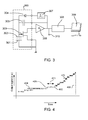
- Figure 3 schematically shows the detector circuitry of a detector equipped with a silicon drift diode.
- a silicon wafer 200 comprises an intrinsic volume 300 in which photons generate electron/hole pairs.
- the intrinsic volume is part of a diode with a cathode 302 and an anode 301.
- the electrons of the electron/hole pair drift towards the cathode, and the holes are collected at anode.
- the gate of a FET 303 placed on the wafer is connected to the cathode, and its source is connected to an amplifier 306 that is placed outside the wafer.
- a capacitor 305 on the wafer provides a feed-back from the output of the amplifier to the gate of the FET, thereby causing the FET and amplifier to act as a charge amplifier.
- a pulse generator 307 monitors the output signal of the charge amplifier, and when its voltage rises above a threshold level, a pulse is generated that, via a diode 304 on the wafer, discharges the capacitance and thereby resets the charge amplifier.
- the signal at the output of the charge amplifier, present on pin 310, is fed to a signal processor 308, which processes the signal and generates a spectrum on monitor 309.
- the signal processor may also provide information of the sample in another way, for example by giving a list of elements and their abundance, or by providing a list of possible mineral composition.
- the latter is especially attractive when the processor cooperates with, for example, the positional resolution capabilities of a Scanning Electron Microscope or the like, and an image is provided that shows position dependent material composition in, for example, false color coded images.
- Figure 4 schematically shows the output signal of the silicon drift detector after the charge amplifier, at pin 310 (see figure 3 ).
- the output signal typically a voltage, shows a number of steps, for example steps 401 and 402, separated by an interval, for example interval 403. These steps are the result of a photon impinging on the diode.
- the height of the step varies, and is a measure for the energy of the photon.
- the signal can be filtered or smoothed during the interval between steps, resulting in a value with a lower variance than the variance of an interval that is smoothed over a smaller interval.
- the variance of the step height of step 401 is thus smaller than the variance of the step height of step 405, as step 401 is surrounded by two intervals that are longer than the two intervals surrounding step 405. It is further shown that, when the signal exceeds a predetermined level, the charge amplifier is reset, resulting in a drop of the signal 406.
- Figure 5 schematically shows the result of the 1/variance of the steps determined from a simulated signal.
- a simulation of a signal is modeled showing a realistic model of noise, containing four distinct components:
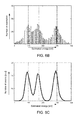
- Figure 6 schematically shows the results of a (simulated) output signal using three different shapers, obtained from the same input signal.
- the input signal is a simulated signal with three spectral lines at 100 eV, 170 eV and 300 eV.
- a number of bins or intervals are arranged along the horizontal or energy axis.
- Vertical is the number of events in each of the bins or energy intervals.
- each event is represented by a Gaussian curve with a variance ⁇ according to the estimated variance, scaled by 1/ ⁇ 2 . It is noted that a Gaussian has a unity integral, and thus a Gaussian with a smaller variance has a higher peak value than a Gaussian with a higher variance.
- scaling (multiplying) it with 1/ ⁇ 2 the integral of the curve is modulated
- figure 6B the output signal obtained using an adaptive filter with a time constant ⁇ between 200 ns and 25 ⁇ s
- figure 6C the output signal obtained using weighted filtering according to the invention.
- Using the fixed filter only 1676 events were registered, the rest being lost by pile-up: the next event(s) arriving within the filter time. Pile-up can be detected, and typically results in two (or more) pulses being rejected.
- the statistics of this output signal are poor, and the energy lines at 100 and 170 eV can not be resolved.
- Figure 6B is the output signal obtained using an adaptive filter with a time constant ⁇ between 200 ns and 25 ⁇ s. Using the adaptive filter 3452 events are registered. The three energy lines at 100, 170 and 300 eV can be resolved.
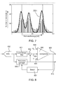
- Figure 7 schematically shows a comparison of spectra obtained from an input signal using a adaptive filter and a filter according to the invention.
- Figure 7 schematically shows a comparison of the output signal obtained from a simulated input signal comprising ca. 6 ⁇ 10 5 samples or events, using the adaptive filter with a time constant ⁇ between 200 ns and 25 ⁇ s (also used in figure 6 b ), and the weighted filter according to the invention.
- the bars shown correspond to the bins in which the results of the adaptive filter are represented, while the curve 701 is the addition of all the Gaussians multiplied by a weight factor resulting from the weighted filtering.
- the output signal 701 according to the invention is better resolved and better defined than the signal obtained with adaptive filtering.
- a Gaussian multiplied by an emphasis factor is used for each of the steps.
- other distributions are successfully used in which a lower variance resulted in a higher peak-value.
- a very useful distribution is, for example, a bar with a standard width and a height that is a function of the variance, to be added/integrated in a histogram (like the bars obtained in the prior art method).
- Figure 8 schematically shows a one-dimensional recursive bilateral filter.
- the idea uses a one-dimensional recursive bilateral filter that continuously adapts its filter bandwidth to the deviation of "future" input samples with the actual output of the filter.
- the input signal is sampled by an analog-to-digital convertor (ADC) 800, resulting in an output signal S(t).
- a look-ahead filter 801 effectively averages n samples, for example four samples.
- V(t) is the output signal of the recursive filter at time t and ⁇ the filter constant.
- the output signals of both filters are subtracted from each other in subtractor 802.
- comparator 806 outputs a signal 809 that, via selector 807, forces the recursive average to use a low ⁇ . This will result in a large noise suppression that will help in reduction of false triggers.
- the look-ahead filter When the input signal rises the look-ahead filter immediately follows this and the signal of the subtractor rises above the threshold T h . As a result the comparator is triggered, causing a signal indicating that a pulse is detected. At the same time a higher ⁇ value is taken for the recursive average, resulting in minimal filtering. This ensures a fast tracking of the input signal during the rise time of the input signal.
- the difference of output signal with the look-ahead filter output is smaller than a predetermined lower threshold T l 805 the recursive average switches back to maximum filtering with low ⁇ constant.
- the output signal 810 of the recursive average 808 can be used for further processing and determining the step height, although also the output signal of the ADC 800 can be used.
- the output 809 of the comparator 806 can be used for pile-up detection etc.
- a slope value is calculated on each plateau by dividing the length of the plateau in three equidistant parts of which the first and last are subtracted. This gives an estimate which is very close to the ideal least means square line fit. It is worthwhile to mention that this method differs from the method described in US patent number US8039787B2 where an improved method for slope determination is described by dividing the single plateau in two sections. In fact, the division in three regions (and not in two as described in the patent) is the optimal method in terms of accuracy and white noise if the ideal least mean square fit is considered to be too expense in terms of FPGA (Field Programmable Gate Array) resources.
- FPGA Field Programmable Gate Array
- an X-ray detector more specifically a SDD
- a SDD is used as the sensor producing the signal.
- sensors for detecting the energy of an event such as radiation sensors for detecting (deep)-UV photons, or particulate radiation comprising, for example, neutrons, electrons or ions, produce a similar signal. Together such sensors are referred to as radiation sensors.
Landscapes
- Physics & Mathematics (AREA)
- General Physics & Mathematics (AREA)
- Spectroscopy & Molecular Physics (AREA)
- Engineering & Computer Science (AREA)
- Life Sciences & Earth Sciences (AREA)
- Molecular Biology (AREA)
- High Energy & Nuclear Physics (AREA)
- Health & Medical Sciences (AREA)
- Data Mining & Analysis (AREA)
- Pure & Applied Mathematics (AREA)
- Theoretical Computer Science (AREA)
- Mathematical Physics (AREA)
- Computational Mathematics (AREA)
- Mathematical Analysis (AREA)
- Mathematical Optimization (AREA)
- Evolutionary Biology (AREA)
- Probability & Statistics with Applications (AREA)
- Operations Research (AREA)
- Algebra (AREA)
- Bioinformatics & Computational Biology (AREA)
- Databases & Information Systems (AREA)
- Software Systems (AREA)
- General Engineering & Computer Science (AREA)
- Bioinformatics & Cheminformatics (AREA)
- Analysing Materials By The Use Of Radiation (AREA)
- Measurement Of Radiation (AREA)
Priority Applications (1)
| Application Number | Priority Date | Filing Date | Title |
|---|---|---|---|
| EP13164043.5A EP2653892B1 (de) | 2012-04-19 | 2013-04-17 | Verfahren zur Analyse eines EDS-Signals |
Applications Claiming Priority (2)
| Application Number | Priority Date | Filing Date | Title |
|---|---|---|---|
| EP12164724.2A EP2653891A1 (de) | 2012-04-19 | 2012-04-19 | Verfahren zur Analyse eines EDS-Signals |
| EP13164043.5A EP2653892B1 (de) | 2012-04-19 | 2013-04-17 | Verfahren zur Analyse eines EDS-Signals |
Publications (3)
| Publication Number | Publication Date |
|---|---|
| EP2653892A2 true EP2653892A2 (de) | 2013-10-23 |
| EP2653892A3 EP2653892A3 (de) | 2014-05-21 |
| EP2653892B1 EP2653892B1 (de) | 2016-06-08 |
Family
ID=48083064
Family Applications (2)
| Application Number | Title | Priority Date | Filing Date |
|---|---|---|---|
| EP12164724.2A Withdrawn EP2653891A1 (de) | 2012-04-19 | 2012-04-19 | Verfahren zur Analyse eines EDS-Signals |
| EP13164043.5A Active EP2653892B1 (de) | 2012-04-19 | 2013-04-17 | Verfahren zur Analyse eines EDS-Signals |
Family Applications Before (1)
| Application Number | Title | Priority Date | Filing Date |
|---|---|---|---|
| EP12164724.2A Withdrawn EP2653891A1 (de) | 2012-04-19 | 2012-04-19 | Verfahren zur Analyse eines EDS-Signals |
Country Status (4)
| Country | Link |
|---|---|
| US (1) | US9361275B2 (de) |
| EP (2) | EP2653891A1 (de) |
| JP (1) | JP6202870B2 (de) |
| CN (1) | CN103376456B (de) |
Cited By (1)
| Publication number | Priority date | Publication date | Assignee | Title |
|---|---|---|---|---|
| EP3062126A1 (de) | 2015-02-26 | 2016-08-31 | FEI Company | Impulsverarbeitung |
Families Citing this family (11)
| Publication number | Priority date | Publication date | Assignee | Title |
|---|---|---|---|---|
| JP6289339B2 (ja) * | 2014-10-28 | 2018-03-07 | 株式会社日立ハイテクノロジーズ | 荷電粒子線装置及び情報処理装置 |
| EP3040714A1 (de) | 2014-12-30 | 2016-07-06 | Fei Company | Ladungsträgerteilchenmikroskop mit verbesserter spektroskopischer Funktionalität |
| DE112018002842T5 (de) | 2017-06-05 | 2020-02-20 | Fondazione Bruno Kessler | Strahlungsdetektor und strahlungsdetektionsvorrichtung |
| JP6574957B2 (ja) * | 2017-09-29 | 2019-09-18 | 株式会社リガク | X線分析用信号処理装置及びx線分析用信号処理装置の調整方法 |
| JP7059089B2 (ja) * | 2018-04-23 | 2022-04-25 | 株式会社日立製作所 | X線検出器およびそれを用いたx線計測装置 |
| DE102019104710B4 (de) * | 2019-02-25 | 2023-04-27 | Ketek Gmbh | Verfahren zum Betreiben eines Strahlungsdetektionssystems und Strahlungsdetektionssystem |
| CN110376229B (zh) | 2019-06-12 | 2020-09-04 | 聚束科技(北京)有限公司 | 具备复合式探测系统的扫描电子显微镜和样品探测方法 |
| JP7403517B2 (ja) * | 2021-10-13 | 2023-12-22 | 日本電子株式会社 | 放射線検出装置および試料分析装置 |
| US12266086B2 (en) * | 2022-02-22 | 2025-04-01 | V-Silicon Semiconductor (Hefei) Co., Ltd | Mosquito noise filtering |
| DE102024122008A1 (de) * | 2024-08-01 | 2026-02-05 | Carl Zeiss Microscopy Gmbh | Verfahren zum Betreiben eines Teilchenstrahlmikroskops |
| CN119224031A (zh) * | 2024-11-01 | 2024-12-31 | 费勉仪器科技(上海)有限公司 | X射线光电子能谱的处理方法以及x射线光电子能谱系统 |
Citations (4)
| Publication number | Priority date | Publication date | Assignee | Title |
|---|---|---|---|---|
| US20060126763A1 (en) | 2004-12-15 | 2006-06-15 | Eric Barat | Processing of a signal representing radiation |
| US7855370B2 (en) | 2007-08-03 | 2010-12-21 | Pulsetor, Llc | Pileup rejection in an energy-dispersive radiation spectrometry system |
| US7966155B2 (en) | 2004-06-04 | 2011-06-21 | William K. Warburton | Method and apparatus for improving detection limits in x-ray and nuclear spectroscopy systems |
| US8039787B2 (en) | 2007-08-03 | 2011-10-18 | Pulsetor, Llc | Digital pulse processor slope correction |
Family Cites Families (13)
| Publication number | Priority date | Publication date | Assignee | Title |
|---|---|---|---|---|
| HU210832B (en) * | 1986-05-07 | 1995-08-28 | Mta Atommag Kutato Intezete | Method for processing signals and adaptive implementation of said method for nuclear spectrometers |
| DE69413304T2 (de) * | 1993-03-24 | 1999-05-12 | Koninklijke Philips Electronics N.V., Eindhoven | Strahlungsuntersuchungsgerät |
| US5349193A (en) * | 1993-05-20 | 1994-09-20 | Princeton Gamma Tech, Inc. | Highly sensitive nuclear spectrometer apparatus and method |
| SE501709C2 (sv) * | 1993-09-09 | 1995-05-02 | Unfors Instr Ab | Metod och instrument för mätning av röntgenstrålning |
| JPH11195123A (ja) * | 1998-01-06 | 1999-07-21 | Hitachi Eng & Service Co Ltd | X線動画形成方法および装置 |
| EP1042690A4 (de) * | 1998-05-09 | 2003-05-21 | Canberra Ind Inc | Digitale impuls-entschlüsselung für strahlungs-spektroskopie |
| US6590957B1 (en) * | 2002-03-13 | 2003-07-08 | William K. Warburton | Method and apparatus for producing spectra corrected for deadtime losses in spectroscopy systems operating under variable input rate conditions |
| US7490009B2 (en) | 2004-08-03 | 2009-02-10 | Fei Company | Method and system for spectroscopic data analysis |
| US7741609B2 (en) * | 2007-08-03 | 2010-06-22 | Pulsetor, Llc | Adapting a high-performance pulse processor to an existing spectrometry system |
| CN103776855B (zh) | 2008-02-06 | 2017-05-31 | Fei 公司 | 谱数据分析的方法和系统 |
| US7807973B2 (en) * | 2008-08-01 | 2010-10-05 | Pulsetor, Llc | Pileup rejection in an energy-dispersive radiation spectrometry system |
| EP2605005A1 (de) | 2011-12-14 | 2013-06-19 | FEI Company | Clustern von multimodalen Daten |
| US8716673B2 (en) | 2011-11-29 | 2014-05-06 | Fei Company | Inductively coupled plasma source as an electron beam source for spectroscopic analysis |
-
2012
- 2012-04-19 EP EP12164724.2A patent/EP2653891A1/de not_active Withdrawn
-
2013
- 2013-04-17 EP EP13164043.5A patent/EP2653892B1/de active Active
- 2013-04-18 JP JP2013087150A patent/JP6202870B2/ja active Active
- 2013-04-19 CN CN201310139086.1A patent/CN103376456B/zh not_active Expired - Fee Related
- 2013-04-19 US US13/866,484 patent/US9361275B2/en active Active
Patent Citations (4)
| Publication number | Priority date | Publication date | Assignee | Title |
|---|---|---|---|---|
| US7966155B2 (en) | 2004-06-04 | 2011-06-21 | William K. Warburton | Method and apparatus for improving detection limits in x-ray and nuclear spectroscopy systems |
| US20060126763A1 (en) | 2004-12-15 | 2006-06-15 | Eric Barat | Processing of a signal representing radiation |
| US7855370B2 (en) | 2007-08-03 | 2010-12-21 | Pulsetor, Llc | Pileup rejection in an energy-dispersive radiation spectrometry system |
| US8039787B2 (en) | 2007-08-03 | 2011-10-18 | Pulsetor, Llc | Digital pulse processor slope correction |
Cited By (2)
| Publication number | Priority date | Publication date | Assignee | Title |
|---|---|---|---|---|
| EP3062126A1 (de) | 2015-02-26 | 2016-08-31 | FEI Company | Impulsverarbeitung |
| EP3062125A1 (de) | 2015-02-26 | 2016-08-31 | Fei Company | Impulsverarbeitung |
Also Published As
| Publication number | Publication date |
|---|---|
| CN103376456A (zh) | 2013-10-30 |
| JP6202870B2 (ja) | 2017-09-27 |
| JP2013224938A (ja) | 2013-10-31 |
| CN103376456B (zh) | 2017-09-08 |
| EP2653892B1 (de) | 2016-06-08 |
| US9361275B2 (en) | 2016-06-07 |
| EP2653892A3 (de) | 2014-05-21 |
| EP2653891A1 (de) | 2013-10-23 |
| US20130277555A1 (en) | 2013-10-24 |
Similar Documents
| Publication | Publication Date | Title |
|---|---|---|
| EP2653892B1 (de) | Verfahren zur Analyse eines EDS-Signals | |
| JP6352529B2 (ja) | 光量検出装置、それを用いた免疫分析装置および荷電粒子線装置 | |
| US10453648B2 (en) | Charged particle bean device and information-processing device | |
| KR102239319B1 (ko) | 시분해 단일 광자 계수 장치 | |
| JP7041079B2 (ja) | スペクトル放射線ディテクターにおける改善された光子カウント | |
| US9245711B2 (en) | Charged particle beam apparatus and image forming method | |
| US9268036B2 (en) | Radiation detector and sample analyzer | |
| US5715049A (en) | Light measuring apparatus for quantifying photons | |
| US10692691B2 (en) | Pulse processing | |
| US8093567B2 (en) | Method and system for counting secondary particles | |
| US9188552B2 (en) | X-ray spectrometer and sample analyzer | |
| US20190033469A1 (en) | Method for processing a pulse generated by a detector of ionizing radiation | |
| CN117784212A (zh) | 一种基于参数扫描的Timepix3探测器能量标定方法 | |
| Abbene et al. | Performance of a digital CdTe X-ray spectrometer in low and high counting rate environment | |
| US10748741B2 (en) | X-ray analyzer and method for correcting counting rate | |
| WO2015186202A1 (ja) | 走査型電子顕微鏡装置 | |
| CN116457663B (zh) | 使用x射线荧光进行生物分析物研究的装置和方法 | |
| US7912657B2 (en) | Method and system for providing a compensated auger spectrum | |
| JP2003202292A (ja) | 蛍光寿命測定装置および方法 | |
| EP4166991B1 (de) | Strahlungsdetektionsvorrichtung und probenanalysevorrichtung | |
| Mott | Improved coincidence rejection for silicon drift detectors | |
| CN121069336A (zh) | 海洋激光雷达波形光子化与后脉冲去除方法与系统 | |
| EP1329699A1 (de) | Optische messvorrichtung und verfahren zur optischen messung | |
| JP2017512984A (ja) | 光子放射を検出するための、特に高フラックス放射に適用されるツール |
Legal Events
| Date | Code | Title | Description |
|---|---|---|---|
| PUAI | Public reference made under article 153(3) epc to a published international application that has entered the european phase |
Free format text: ORIGINAL CODE: 0009012 |
|
| AK | Designated contracting states |
Kind code of ref document: A2 Designated state(s): AL AT BE BG CH CY CZ DE DK EE ES FI FR GB GR HR HU IE IS IT LI LT LU LV MC MK MT NL NO PL PT RO RS SE SI SK SM TR |
|
| AX | Request for extension of the european patent |
Extension state: BA ME |
|
| PUAL | Search report despatched |
Free format text: ORIGINAL CODE: 0009013 |
|
| AK | Designated contracting states |
Kind code of ref document: A3 Designated state(s): AL AT BE BG CH CY CZ DE DK EE ES FI FR GB GR HR HU IE IS IT LI LT LU LV MC MK MT NL NO PL PT RO RS SE SI SK SM TR |
|
| AX | Request for extension of the european patent |
Extension state: BA ME |
|
| RIC1 | Information provided on ipc code assigned before grant |
Ipc: G01T 1/36 20060101ALI20140415BHEP Ipc: G01T 1/17 20060101AFI20140415BHEP |
|
| 17P | Request for examination filed |
Effective date: 20140505 |
|
| RBV | Designated contracting states (corrected) |
Designated state(s): AL AT BE BG CH CY CZ DE DK EE ES FI FR GB GR HR HU IE IS IT LI LT LU LV MC MK MT NL NO PL PT RO RS SE SI SK SM TR |
|
| GRAP | Despatch of communication of intention to grant a patent |
Free format text: ORIGINAL CODE: EPIDOSNIGR1 |
|
| INTG | Intention to grant announced |
Effective date: 20160125 |
|
| GRAS | Grant fee paid |
Free format text: ORIGINAL CODE: EPIDOSNIGR3 |
|
| GRAA | (expected) grant |
Free format text: ORIGINAL CODE: 0009210 |
|
| AK | Designated contracting states |
Kind code of ref document: B1 Designated state(s): AL AT BE BG CH CY CZ DE DK EE ES FI FR GB GR HR HU IE IS IT LI LT LU LV MC MK MT NL NO PL PT RO RS SE SI SK SM TR |
|
| REG | Reference to a national code |
Ref country code: GB Ref legal event code: FG4D |
|
| REG | Reference to a national code |
Ref country code: CH Ref legal event code: EP |
|
| REG | Reference to a national code |
Ref country code: IE Ref legal event code: FG4D |
|
| REG | Reference to a national code |
Ref country code: AT Ref legal event code: REF Ref document number: 805632 Country of ref document: AT Kind code of ref document: T Effective date: 20160715 |
|
| REG | Reference to a national code |
Ref country code: DE Ref legal event code: R096 Ref document number: 602013008319 Country of ref document: DE |
|
| REG | Reference to a national code |
Ref country code: LT Ref legal event code: MG4D |
|
| REG | Reference to a national code |
Ref country code: NL Ref legal event code: MP Effective date: 20160608 |
|
| PG25 | Lapsed in a contracting state [announced via postgrant information from national office to epo] |
Ref country code: FI Free format text: LAPSE BECAUSE OF FAILURE TO SUBMIT A TRANSLATION OF THE DESCRIPTION OR TO PAY THE FEE WITHIN THE PRESCRIBED TIME-LIMIT Effective date: 20160608 Ref country code: LT Free format text: LAPSE BECAUSE OF FAILURE TO SUBMIT A TRANSLATION OF THE DESCRIPTION OR TO PAY THE FEE WITHIN THE PRESCRIBED TIME-LIMIT Effective date: 20160608 Ref country code: NO Free format text: LAPSE BECAUSE OF FAILURE TO SUBMIT A TRANSLATION OF THE DESCRIPTION OR TO PAY THE FEE WITHIN THE PRESCRIBED TIME-LIMIT Effective date: 20160908 |
|
| REG | Reference to a national code |
Ref country code: AT Ref legal event code: MK05 Ref document number: 805632 Country of ref document: AT Kind code of ref document: T Effective date: 20160608 |
|
| PG25 | Lapsed in a contracting state [announced via postgrant information from national office to epo] |
Ref country code: HR Free format text: LAPSE BECAUSE OF FAILURE TO SUBMIT A TRANSLATION OF THE DESCRIPTION OR TO PAY THE FEE WITHIN THE PRESCRIBED TIME-LIMIT Effective date: 20160608 Ref country code: ES Free format text: LAPSE BECAUSE OF FAILURE TO SUBMIT A TRANSLATION OF THE DESCRIPTION OR TO PAY THE FEE WITHIN THE PRESCRIBED TIME-LIMIT Effective date: 20160608 Ref country code: NL Free format text: LAPSE BECAUSE OF FAILURE TO SUBMIT A TRANSLATION OF THE DESCRIPTION OR TO PAY THE FEE WITHIN THE PRESCRIBED TIME-LIMIT Effective date: 20160608 Ref country code: LV Free format text: LAPSE BECAUSE OF FAILURE TO SUBMIT A TRANSLATION OF THE DESCRIPTION OR TO PAY THE FEE WITHIN THE PRESCRIBED TIME-LIMIT Effective date: 20160608 Ref country code: SE Free format text: LAPSE BECAUSE OF FAILURE TO SUBMIT A TRANSLATION OF THE DESCRIPTION OR TO PAY THE FEE WITHIN THE PRESCRIBED TIME-LIMIT Effective date: 20160608 Ref country code: GR Free format text: LAPSE BECAUSE OF FAILURE TO SUBMIT A TRANSLATION OF THE DESCRIPTION OR TO PAY THE FEE WITHIN THE PRESCRIBED TIME-LIMIT Effective date: 20160909 Ref country code: RS Free format text: LAPSE BECAUSE OF FAILURE TO SUBMIT A TRANSLATION OF THE DESCRIPTION OR TO PAY THE FEE WITHIN THE PRESCRIBED TIME-LIMIT Effective date: 20160608 |
|
| PG25 | Lapsed in a contracting state [announced via postgrant information from national office to epo] |
Ref country code: EE Free format text: LAPSE BECAUSE OF FAILURE TO SUBMIT A TRANSLATION OF THE DESCRIPTION OR TO PAY THE FEE WITHIN THE PRESCRIBED TIME-LIMIT Effective date: 20160608 Ref country code: SK Free format text: LAPSE BECAUSE OF FAILURE TO SUBMIT A TRANSLATION OF THE DESCRIPTION OR TO PAY THE FEE WITHIN THE PRESCRIBED TIME-LIMIT Effective date: 20160608 Ref country code: RO Free format text: LAPSE BECAUSE OF FAILURE TO SUBMIT A TRANSLATION OF THE DESCRIPTION OR TO PAY THE FEE WITHIN THE PRESCRIBED TIME-LIMIT Effective date: 20160608 Ref country code: CZ Free format text: LAPSE BECAUSE OF FAILURE TO SUBMIT A TRANSLATION OF THE DESCRIPTION OR TO PAY THE FEE WITHIN THE PRESCRIBED TIME-LIMIT Effective date: 20160608 Ref country code: IT Free format text: LAPSE BECAUSE OF FAILURE TO SUBMIT A TRANSLATION OF THE DESCRIPTION OR TO PAY THE FEE WITHIN THE PRESCRIBED TIME-LIMIT Effective date: 20160608 Ref country code: IS Free format text: LAPSE BECAUSE OF FAILURE TO SUBMIT A TRANSLATION OF THE DESCRIPTION OR TO PAY THE FEE WITHIN THE PRESCRIBED TIME-LIMIT Effective date: 20161008 |
|
| PG25 | Lapsed in a contracting state [announced via postgrant information from national office to epo] |
Ref country code: PL Free format text: LAPSE BECAUSE OF FAILURE TO SUBMIT A TRANSLATION OF THE DESCRIPTION OR TO PAY THE FEE WITHIN THE PRESCRIBED TIME-LIMIT Effective date: 20160608 Ref country code: BE Free format text: LAPSE BECAUSE OF FAILURE TO SUBMIT A TRANSLATION OF THE DESCRIPTION OR TO PAY THE FEE WITHIN THE PRESCRIBED TIME-LIMIT Effective date: 20160608 Ref country code: PT Free format text: LAPSE BECAUSE OF FAILURE TO SUBMIT A TRANSLATION OF THE DESCRIPTION OR TO PAY THE FEE WITHIN THE PRESCRIBED TIME-LIMIT Effective date: 20161010 Ref country code: AT Free format text: LAPSE BECAUSE OF FAILURE TO SUBMIT A TRANSLATION OF THE DESCRIPTION OR TO PAY THE FEE WITHIN THE PRESCRIBED TIME-LIMIT Effective date: 20160608 Ref country code: SM Free format text: LAPSE BECAUSE OF FAILURE TO SUBMIT A TRANSLATION OF THE DESCRIPTION OR TO PAY THE FEE WITHIN THE PRESCRIBED TIME-LIMIT Effective date: 20160608 |
|
| REG | Reference to a national code |
Ref country code: DE Ref legal event code: R097 Ref document number: 602013008319 Country of ref document: DE |
|
| REG | Reference to a national code |
Ref country code: FR Ref legal event code: PLFP Year of fee payment: 5 |
|
| PLBE | No opposition filed within time limit |
Free format text: ORIGINAL CODE: 0009261 |
|
| STAA | Information on the status of an ep patent application or granted ep patent |
Free format text: STATUS: NO OPPOSITION FILED WITHIN TIME LIMIT |
|
| 26N | No opposition filed |
Effective date: 20170309 |
|
| PG25 | Lapsed in a contracting state [announced via postgrant information from national office to epo] |
Ref country code: DK Free format text: LAPSE BECAUSE OF FAILURE TO SUBMIT A TRANSLATION OF THE DESCRIPTION OR TO PAY THE FEE WITHIN THE PRESCRIBED TIME-LIMIT Effective date: 20160608 Ref country code: SI Free format text: LAPSE BECAUSE OF FAILURE TO SUBMIT A TRANSLATION OF THE DESCRIPTION OR TO PAY THE FEE WITHIN THE PRESCRIBED TIME-LIMIT Effective date: 20160608 |
|
| REG | Reference to a national code |
Ref country code: CH Ref legal event code: PL |
|
| REG | Reference to a national code |
Ref country code: IE Ref legal event code: MM4A |
|
| PG25 | Lapsed in a contracting state [announced via postgrant information from national office to epo] |
Ref country code: MC Free format text: LAPSE BECAUSE OF FAILURE TO SUBMIT A TRANSLATION OF THE DESCRIPTION OR TO PAY THE FEE WITHIN THE PRESCRIBED TIME-LIMIT Effective date: 20160608 |
|
| PG25 | Lapsed in a contracting state [announced via postgrant information from national office to epo] |
Ref country code: LU Free format text: LAPSE BECAUSE OF NON-PAYMENT OF DUE FEES Effective date: 20170417 Ref country code: LI Free format text: LAPSE BECAUSE OF NON-PAYMENT OF DUE FEES Effective date: 20170430 Ref country code: CH Free format text: LAPSE BECAUSE OF NON-PAYMENT OF DUE FEES Effective date: 20170430 |
|
| REG | Reference to a national code |
Ref country code: FR Ref legal event code: PLFP Year of fee payment: 6 |
|
| PG25 | Lapsed in a contracting state [announced via postgrant information from national office to epo] |
Ref country code: IE Free format text: LAPSE BECAUSE OF NON-PAYMENT OF DUE FEES Effective date: 20170417 |
|
| PG25 | Lapsed in a contracting state [announced via postgrant information from national office to epo] |
Ref country code: MT Free format text: LAPSE BECAUSE OF NON-PAYMENT OF DUE FEES Effective date: 20170417 |
|
| PG25 | Lapsed in a contracting state [announced via postgrant information from national office to epo] |
Ref country code: AL Free format text: LAPSE BECAUSE OF FAILURE TO SUBMIT A TRANSLATION OF THE DESCRIPTION OR TO PAY THE FEE WITHIN THE PRESCRIBED TIME-LIMIT Effective date: 20160608 |
|
| PG25 | Lapsed in a contracting state [announced via postgrant information from national office to epo] |
Ref country code: HU Free format text: LAPSE BECAUSE OF FAILURE TO SUBMIT A TRANSLATION OF THE DESCRIPTION OR TO PAY THE FEE WITHIN THE PRESCRIBED TIME-LIMIT; INVALID AB INITIO Effective date: 20130417 |
|
| PG25 | Lapsed in a contracting state [announced via postgrant information from national office to epo] |
Ref country code: BG Free format text: LAPSE BECAUSE OF FAILURE TO SUBMIT A TRANSLATION OF THE DESCRIPTION OR TO PAY THE FEE WITHIN THE PRESCRIBED TIME-LIMIT Effective date: 20160608 |
|
| PG25 | Lapsed in a contracting state [announced via postgrant information from national office to epo] |
Ref country code: CY Free format text: LAPSE BECAUSE OF NON-PAYMENT OF DUE FEES Effective date: 20160608 |
|
| PG25 | Lapsed in a contracting state [announced via postgrant information from national office to epo] |
Ref country code: MK Free format text: LAPSE BECAUSE OF FAILURE TO SUBMIT A TRANSLATION OF THE DESCRIPTION OR TO PAY THE FEE WITHIN THE PRESCRIBED TIME-LIMIT Effective date: 20160608 |
|
| PG25 | Lapsed in a contracting state [announced via postgrant information from national office to epo] |
Ref country code: TR Free format text: LAPSE BECAUSE OF FAILURE TO SUBMIT A TRANSLATION OF THE DESCRIPTION OR TO PAY THE FEE WITHIN THE PRESCRIBED TIME-LIMIT Effective date: 20160608 |
|
| P01 | Opt-out of the competence of the unified patent court (upc) registered |
Effective date: 20230524 |
|
| PGFP | Annual fee paid to national office [announced via postgrant information from national office to epo] |
Ref country code: DE Payment date: 20250314 Year of fee payment: 13 |
|
| PGFP | Annual fee paid to national office [announced via postgrant information from national office to epo] |
Ref country code: FR Payment date: 20250403 Year of fee payment: 13 |
|
| PGFP | Annual fee paid to national office [announced via postgrant information from national office to epo] |
Ref country code: GB Payment date: 20260311 Year of fee payment: 14 |