EP2653879A1 - Device for the simultaneous output of a direct voltage signal with a non-linear power-voltage curve - Google Patents
Device for the simultaneous output of a direct voltage signal with a non-linear power-voltage curve Download PDFInfo
- Publication number
- EP2653879A1 EP2653879A1 EP13162207.8A EP13162207A EP2653879A1 EP 2653879 A1 EP2653879 A1 EP 2653879A1 EP 13162207 A EP13162207 A EP 13162207A EP 2653879 A1 EP2653879 A1 EP 2653879A1
- Authority
- EP
- European Patent Office
- Prior art keywords
- voltage source
- linear
- voltage
- signal output
- output
- Prior art date
- Legal status (The legal status is an assumption and is not a legal conclusion. Google has not performed a legal analysis and makes no representation as to the accuracy of the status listed.)
- Granted
Links
- 238000012360 testing method Methods 0.000 claims description 63
- 238000009434 installation Methods 0.000 claims description 4
- 238000005259 measurement Methods 0.000 description 5
- 230000000903 blocking effect Effects 0.000 description 2
- 238000011161 development Methods 0.000 description 2
- 238000010438 heat treatment Methods 0.000 description 2
- 230000001419 dependent effect Effects 0.000 description 1
- 238000002844 melting Methods 0.000 description 1
- 230000008018 melting Effects 0.000 description 1
- 238000000034 method Methods 0.000 description 1
- 238000011056 performance test Methods 0.000 description 1
- 230000001681 protective effect Effects 0.000 description 1
- 230000002441 reversible effect Effects 0.000 description 1
- 238000004513 sizing Methods 0.000 description 1
- 230000002123 temporal effect Effects 0.000 description 1
Images


Classifications
-
- G—PHYSICS
- G01—MEASURING; TESTING
- G01R—MEASURING ELECTRIC VARIABLES; MEASURING MAGNETIC VARIABLES
- G01R31/00—Arrangements for testing electric properties; Arrangements for locating electric faults; Arrangements for electrical testing characterised by what is being tested not provided for elsewhere
- G01R31/28—Testing of electronic circuits, e.g. by signal tracer
- G01R31/2832—Specific tests of electronic circuits not provided for elsewhere
- G01R31/2836—Fault-finding or characterising
- G01R31/2839—Fault-finding or characterising using signal generators, power supplies or circuit analysers
- G01R31/2841—Signal generators
-
- H—ELECTRICITY
- H02—GENERATION; CONVERSION OR DISTRIBUTION OF ELECTRIC POWER
- H02S—GENERATION OF ELECTRIC POWER BY CONVERSION OF INFRARED RADIATION, VISIBLE LIGHT OR ULTRAVIOLET LIGHT, e.g. USING PHOTOVOLTAIC [PV] MODULES
- H02S50/00—Monitoring or testing of PV systems, e.g. load balancing or fault identification
- H02S50/10—Testing of PV devices, e.g. of PV modules or single PV cells
-
- G—PHYSICS
- G01—MEASURING; TESTING
- G01R—MEASURING ELECTRIC VARIABLES; MEASURING MAGNETIC VARIABLES
- G01R31/00—Arrangements for testing electric properties; Arrangements for locating electric faults; Arrangements for electrical testing characterised by what is being tested not provided for elsewhere
- G01R31/40—Testing power supplies
-
- Y—GENERAL TAGGING OF NEW TECHNOLOGICAL DEVELOPMENTS; GENERAL TAGGING OF CROSS-SECTIONAL TECHNOLOGIES SPANNING OVER SEVERAL SECTIONS OF THE IPC; TECHNICAL SUBJECTS COVERED BY FORMER USPC CROSS-REFERENCE ART COLLECTIONS [XRACs] AND DIGESTS
- Y02—TECHNOLOGIES OR APPLICATIONS FOR MITIGATION OR ADAPTATION AGAINST CLIMATE CHANGE
- Y02E—REDUCTION OF GREENHOUSE GAS [GHG] EMISSIONS, RELATED TO ENERGY GENERATION, TRANSMISSION OR DISTRIBUTION
- Y02E10/00—Energy generation through renewable energy sources
- Y02E10/50—Photovoltaic [PV] energy
Definitions
- the present invention relates to a device for outputting a DC voltage signal with a nonlinear current-voltage characteristic, in particular for testing a device under test and a simulator for testing electrical devices and installations, in particular photovoltaic components.
- test or test devices which are also referred to below as simulators, which simulate a non-linear voltage-current characteristic curve to which the electrical equipment and systems are exposed during operation can.
- simulators which simulate a non-linear voltage-current characteristic curve to which the electrical equipment and systems are exposed during operation can.
- power sources needed that can simulate non-linear voltage-current characteristics of solar modules.
- Such voltage sources are currently realized by consuming electronic circuits with constant current sources, which are powered by a DC voltage source, e.g. from a transformer-fed rectifier, are fed with a linear characteristic and generate the desired non-linear characteristic by appropriate control of active power electronics modules.
- a DC voltage source e.g. from a transformer-fed rectifier
- the present invention proposes a device for outputting a DC voltage signal with non-linear current-voltage characteristic according to claim 1 and a simulator for testing electrical equipment and installations according to claim 10.
- an apparatus for outputting a DC voltage signal having a non-linear current-voltage characteristic comprises a first signal output, a second signal output, a first linear voltage source, a second linear voltage source, and a switching element.
- the first linear voltage source comprises a negative pole and a positive pole and is set up to output a first DC output voltage between the negative pole and the positive pole.
- the second linear voltage source comprises a negative pole and a positive pole and is adapted to output a second DC output voltage between the negative pole and the positive pole, wherein the positive pole of the second linear voltage source is connected to the negative pole of the first linear voltage source.
- the first signal output is connected via a first series resistor to the positive pole of the first linear voltage source.
- the second signal output is connected via a second series resistor to the negative pole of the second linear voltage source.
- the switching element has a first terminal and a second terminal connected to the second signal output, wherein the first terminal is connected to the negative pole of the first linear voltage source, and wherein the switching element is in a non-conductive state when between the second terminal and the first terminal is a positive voltage difference.
- the switching element comprises a diode, typically a power diode, which is arranged in the forward direction between the positive pole of the second linear voltage source and the negative pole of the second linear voltage source.
- a diode typically a power diode
- the switching element may in particular consist of a diode, typically a power diode. The speed of the switching process is then limited essentially only by the high switching speed of the diode.
- the use of the diode also makes it possible to dispense with power-limiting active components, such as transistors. This makes it possible to provide higher test powers with nonlinear source characteristics.
- a switching point between the non-conducting state and a conducting state of the switching element with an accuracy of 5% or better, e.g. with an accuracy of 3% or better, set at a point of maximum power of the non-linear current-voltage characteristic.
- the non-linear current-voltage current characteristic can be adapted with sufficient accuracy to the non-linear current-voltage current characteristic which comprises a test object, e.g. a fuse, switchgear or arrester may be exposed during normal operation.
- the non-linear current-voltage current characteristic of photovoltaic modules can be used for test purposes of e.g. Generate switching devices and fuses of photovoltaic systems with sufficient accuracy in a simulator.
- the first series resistor and / or the second series resistor is a variable resistor. This makes it possible to easily adjust the nonlinear current-voltage current characteristic.
- the first linear voltage source and / or the second linear voltage source may be e.g. to act as a 6-pulse DC voltage source. This high performance can be provided in a simple manner.
- the second DC output voltage may be equal to or greater than the first DC output voltage depending on the desired non-linear current-voltage current characteristic, e.g. about 3 times as large as the first DC output voltage, if the desired non-linear current-voltage characteristic is to correspond to that of a photovoltaic module.
- the first linear voltage source and / or the second linear voltage source is a switchable linear voltage source.
- the power output of the voltage sources in a simulator can only be limited to the required test times and thus electrical losses and heating can be reduced.
- the apparatus for outputting a DC voltage signal having a nonlinear current-voltage characteristic is arranged to provide DC signals of at least 100 A, more typically more than 200 A, eg more than 500 A, in the event of a short circuit between the first signal output and the second signal output. This allows the device to be used as a voltage source in a performance tester simulator.
- the device is arranged to output a DC voltage signal with non-linear current-voltage characteristic, in the unloaded state between the second signal output and the first signal output DC signals of at least 1000 V, e.g. of more than 1500V. This allows the device to be used as a voltage source in a performance tester simulator.
- the device is provided for outputting a DC voltage signal with a nonlinear current-voltage characteristic, DC signals of DC signals of at least 100 kW, more typically at least 200 kW, more typically at least 400 kW, for example, between the second signal output and the first signal output. of at least 600 kW.
- DC signals of DC signals of at least 100 kW, more typically at least 200 kW, more typically at least 400 kW, for example, between the second signal output and the first signal output. of at least 600 kW.
- This allows the device to be used as a voltage source in a performance tester simulator.
- the device may provide about 386 kW of nonlinear current-voltage characteristics.
- the provided non-linear current-voltage characteristic then corresponds to a typical photovoltaic module with 1575 V open circuit voltage and a short-circuit current of 500 A, the power in point of maximum power corresponds to about 49% of the product of short-circuit current and no-load voltage.
- a simulator for testing electrical devices and installations comprises a first test signal output, a second test signal output, a first linear voltage source, wherein the first linear voltage source comprises a negative pole and a positive pole which is connected to the first test signal output, and is arranged to output a first output voltage between the positive pole and the negative pole, a second linear voltage source, the second linear voltage source having a negative pole which is connected to the second test signal output, and a positive pole which is connected to the negative pole of the first linear voltage source, comprises and is set up to output a second output voltage between the positive pole and the negative pole, and a power diode, which in the forward direction between the positive pole of the second linear voltage source and the negative pole of the second linear voltage source is switched.
- a simple simulator with non-linear current-voltage characteristic between the first test signal output and the second test signal output is provided, which can be carried out without complex Electronic circuits (eg constant current sources) also allow the testing of electrical equipment and systems for
- the simulator comprises a first resistor connected between the positive pole of the first linear voltage source and the first test signal output and / or a second resistor connected between the negative pole of the second voltage source and the diode and the second test signal output. This easily enables the simulator to switch between two linear sections of the non-linear current-voltage characteristic according to a changing resistance of a test object connected between the first test signal output and the second test signal output.
- the first resistor and / or the second resistor is a variable resistor, whereby the non-linear current-voltage current characteristic can be easily adjusted.
- the simulator is arranged between the first test signal output and the second test signal output DC signals of at least 100 kW, more typically at least 200 kW, more typically at least 400 kW, e.g. of at least 600 kW.
- simulator as used herein is intended to mean an electrical test device for a device under test, in particular a performance test object.
- the simulator is arranged to provide the device under test with electrical test signals according to a non-linear current-voltage characteristic, e.g. with electrical test signals, which essentially corresponds to a non-linear voltage-current characteristic curve of a solar module.
- Fig. 1 shows a typical non-linear current-voltage characteristic of a photovoltaic module in relative units.
- a nonlinear current-voltage characteristic is also to be provided by a simulator with sufficient accuracy for testing purposes of photovoltaic components.
- the current-voltage characteristic is determined by at least 3 points: by the short-circuit current I k , the open-circuit voltage U 0 and the point of maximum power MPP ("Maximum Power Point"). It can be described to a good approximation by two linear sections.
- the required performance of the simulator at the point of maximum power can amount to several 100 kW, in particular for the testing of short-circuit protection devices or switching devices.
- the test voltage for the low voltage range is up to 1575 V (1500 V rated voltage + 5%), the test currents are up to a few 100 A depending on the requirements.
- Fig. 2 shows a schematic representation of a voltage source 100 with non-linear current-voltage characteristic with connected load 50, for example.
- a DUT a DUT
- the voltage source 100 is used in or as a simulator for testing the device under test 50.
- the test object 50 is connected between a first signal output 101 or the first test signal output and a second signal output 102 or second test signal output.
- the voltage source 100 or the simulator 100 comprises a first linear voltage source 110, a second linear voltage source connected in series with the first linear voltage source 110 and a switching element D.
- the first linear voltage source 110 has a negative pole 111 and a positive pole 112, between which can output a first DC output voltage U1.
- the second linear voltage source 120 has a negative pole 121 and a positive pole 122, between which it can output a second DC output voltage U2.
- the positive pole 122 of the second linear voltage source 120 is connected to the negative pole 111 of the first linear voltage source 110.
- the first signal output 101 is connected to the positive pole 112 of the first linear voltage source 110 via a first series resistor R1.
- the second signal output 102 is connected via a second series resistor R2 to the negative pole 121 of the second linear voltage source 120.
- the switching element D has a first terminal 103 and a second terminal 104.
- the first terminal 103 has a low-resistance connection to the negative terminal 111 of the first voltage source 110 and to the positive terminal 122 of the second linear voltage source.
- the second output 104 has a low resistance to the second signal output 102 and is connected via the second series resistor R2 to the negative pole 121 of the second linear voltage source 120.
- the switching element D is realized by a diode, typically a power diode.
- a diode typically a power diode.
- other voltage-sensitive switches ie switches which switch in accordance with a voltage applied between their two terminals 103, 104.
- the switching element D is in a non-conducting state when a positive voltage difference is applied between the second terminal 104 and the first terminal 103, ie when between the second signal output 102 and the common reference point of negative terminal 111 of the first voltage source 110 and the positive pole 122 of the second linear voltage source 120 is applied a positive voltage difference.
- the switching element D is typically in a conductive state when a predetermined negative voltage difference is applied between the second terminal 104 and the first terminal 103.
- the switching element D is designed as a diode, the predetermined negative voltage difference corresponds in magnitude to the diode threshold voltage.
- the switching element D may also be in the conductive state when applied to the same voltages at the terminals 103 and 104.
- the use of one or more diodes D allows a simple and robust structure in which the switching point of the diode or the diodes can be set well.
- a simple self-switching power source 100 or a simple self-switching simulator 100 with non-linear current-voltage characteristic can also be realized for high power, without consuming electronic circuits, eg. B. constant current sources and power-limiting power components such as transistors to use.
- the switching element D can be switched between two linear characteristic sections and so signals are output according to a non-linear current-voltage characteristic between the signal outputs 101 and 102.
- the series resistors R1, R2 form a voltage divider with the load resistance RL of the test object 50. Due to the changing load resistance RL of the device under test 50, e.g. during a switching operation of the test object 50, the voltage at the second output 104 changes with respect to the voltage at the first output 103 of the switching element D.
- the series resistor R2 is always current-carrying and correspondingly low-resistance devices under test 50 and the resistor R1, typically switchable voltage sources for the first linear voltage source 110 and the second linear voltage source 120 are used at higher powers to reduce electrical losses and heating. For the testing of switching components, it is possible to represent the required non-linear characteristic only for a sufficient period of time without thermally overloading the resistors.
- the diode D With appropriate dimensioning of the output voltages U1, U2, and the series resistors R1 and R2, the diode D changes its conduction state at a desired switching point MPP maximum power, as it is desirable for testing of photovoltaic components.
- Fig. 3 indicates an expected non-linear current-voltage characteristic of the voltage source 100 Fig. 2
- the factor k is used to denote the relative position of the maximum power point MPP in relation to the short-circuit current or the open-circuit voltage.
- the diode D With this dimensioning, the diode D, ignoring the relatively low threshold voltage, is conductive when the load resistance RL is greater than U 0 / I k , and it turns off when the value becomes smaller than U 0 / I k . The diode D thus switches the nonlinear current-voltage characteristic at the point MPP of maximum power.
- switching element D By using a diode as switching element D, it is possible to rely on power limiting active devices, e.g. Transistors are dispensed with. This makes it possible to provide higher test performance with non-linear characteristics.
- power limiting active devices e.g. Transistors are dispensed with. This makes it possible to provide higher test performance with non-linear characteristics.
- the load on the switching diode D with regard to blocking voltage and current is in the range of current values for power diodes today.
- the occurring reverse voltage is always smaller than the open circuit voltage (test voltage) of eg max. 1575 V.
- the current flowing through the diode D is also always smaller than the short-circuit current (test current) I k .
- Fig. 4 shows a measured non-linear current-voltage characteristic of a voltage source according to Fig. 2 in relative units.
- a load resistor RL By connecting a load resistor RL with different resistance values were in a structure of the circuit 100, as above with reference to the Figures 2 and 3 was explained with an open circuit voltage U 0 of 580 V, a short-circuit current I k of 115 A and a k-factor of 0.78, the measurement points for current and voltage at the load resistance determined.
- a switchable linear voltage source was used as first and second linear voltage source.
- the comparison of the determined current-voltage characteristic with the in FIG. 1 shown desired non-linear current-voltage characteristic of a photovoltaic module shows that their characteristics can be well simulated with the circuit 100.
- the switching point "MPP" can be set with an accuracy better than 5%. This allows meaningful measurements on specimens.
- Fig. 5 shows a test measurement on an 80A fuse as a test object with a simulator 100 as above with reference to the Figures 2 and 3 was explained.
- a circuit 100 with an open circuit voltage U 0 of 1575 V, a short-circuit current I k of about 500 A and a k-factor of 0.7 was used.
- FIG. 6 shown in which the time course of current and voltage in relative units is shown.
- the k-factor can be read directly at the intersection of both lines.
- the power at the point "MPP" maximum power was about 386 kW (equivalent to about 49% of about 787 kW).
- the melting of the fuse can be tracked by means of the simulator 100 under test-relevant electrical conditions with good temporal resolution.
- the power diode used as a switching element switches reliably and sufficiently fast. It goes without saying that in each case a switchable linear voltage source was used as the first and second linear voltage source in order to limit the electrical losses essentially to the actual measuring phase.
Landscapes
- Engineering & Computer Science (AREA)
- General Engineering & Computer Science (AREA)
- Physics & Mathematics (AREA)
- General Physics & Mathematics (AREA)
- Testing Of Individual Semiconductor Devices (AREA)
- Photovoltaic Devices (AREA)
Abstract
Description
Die vorliegende Erfindung betrifft eine Vorrichtung zum Ausgeben eines Gleichspannungssignals mit nichtlinearer Strom-Spannungskennlinie, insbesondere zur Prüfung eines Prüflings sowie einen Simulator zum Prüfen von elektrotechnischen Geräten und Anlagen, insbesondere von Photovoltaikkomponenten.The present invention relates to a device for outputting a DC voltage signal with a nonlinear current-voltage characteristic, in particular for testing a device under test and a simulator for testing electrical devices and installations, in particular photovoltaic components.
Zum Entwickeln und Prüfen elektrotechnischer Geräte und Anlagen werden in entsprechenden Test- bzw. Prüfvorrichtungen, die im Folgenden auch als Simulatoren bezeichnet werden, häufig Spannungsquellen benötigt, die einen nichtlinearen Spannungs-Strom-Kennlinienverlauf nachbilden, dem die elektrotechnischen Geräte und Anlagen im Betrieb ausgesetzt sein können. Beispielsweise werden für die Entwicklung und Prüfung der Komponenten von Photovoltaik-Anlagen, wie z.B. Schutzeinrichtungen und Schaltgeräten, Spannungsquellen benötigt, die nichtlineare Spannungs-Strom-Kennlinienverläufe von Solarmodulen nachbilden können.To develop and test electrical equipment and systems voltage sources are often required in corresponding test or test devices, which are also referred to below as simulators, which simulate a non-linear voltage-current characteristic curve to which the electrical equipment and systems are exposed during operation can. For example, for the development and testing of the components of photovoltaic systems, such as e.g. Protective devices and switching devices, power sources needed that can simulate non-linear voltage-current characteristics of solar modules.
Derartige Spannungsquellen werden gegenwärtig durch aufwändige elektronische Schaltungen mit Konstantstromquellen realisiert, welche von einer Gleichspannungsquelle, z.B. von einem transformatorgespeisten Gleichrichter, mit linearer Kennlinie gespeist werden und durch entsprechende Ansteuerung aktiver leistungselektronischer Baugruppen die gewünschte nichtlineare Kennlinie erzeugen.Such voltage sources are currently realized by consuming electronic circuits with constant current sources, which are powered by a DC voltage source, e.g. from a transformer-fed rectifier, are fed with a linear characteristic and generate the desired non-linear characteristic by appropriate control of active power electronics modules.
Die Leistung dieser elektronischen Prüfquellen liegt z.Zt. bei maximal etwa 150 kW (bei 1500 V). Sie wird von den Kennwerten der leistungselektronischen Bauelemente, meist Transistoren, bestimmt und begrenzt. Das ist für die Prüfung von Kurzschlussschutzeinrichtungen und Schaltgeräten mitunter nicht ausreichend.The performance of these electronic test sources is currently. at a maximum of about 150 kW (at 1500 V). It is determined and limited by the characteristics of the power electronic components, usually transistors. This is sometimes not sufficient for testing short-circuit protection devices and switching devices.
Im Hinblick auf das oben Gesagte, schlägt die vorliegende Erfindung eine Vorrichtung zur Ausgabe eines Gleichspannungssignals mit nichtlinearer Strom-Spannungskennlinie gemäß Anspruch 1 und einen Simulator zum Prüfen von elektrotechnischen Geräten und Anlagen gemäß Anspruch 10 vor.In view of the above, the present invention proposes a device for outputting a DC voltage signal with non-linear current-voltage characteristic according to
Gemäß einem Ausführungsbeispiel umfasst eine Vorrichtung zum Ausgeben eines Gleichspannungssignals mit nichtlinearer Strom-Spannungskennlinie, einen ersten Signalausgang, einen zweiten Signalausgang, eine erste lineare Spannungsquelle, eine zweite lineare Spannungsquelle und ein Schaltelement. Die erste lineare Spannungsquelle umfasst einen Minuspol und einen Pluspol und ist eingerichtet ist, zwischen dem Minuspol und dem Pluspol eine erste Ausgangsgleichspannung auszugeben. Die zweite lineare Spannungsquelle umfasst einen Minuspol und einen Pluspol und ist eingerichtet, zwischen dem Minuspol und dem Pluspol eine zweite Ausgangsgleichspannung auszugeben, wobei der Pluspol der zweiten linearen Spannungsquelle mit dem Minuspol der ersten linearen Spannungsquelle verbunden ist. Der erste Signalausgang ist über einen ersten Vorwiderstand mit dem Pluspol der ersten linearen Spannungsquelle verbunden. Der zweite Signalausgang ist über einen zweiten Vorwiderstand mit dem Minuspol der zweiten linearen Spannungsquelle verbunden. Das Schaltelement hat einem ersten Anschluss und einem zweiten Anschluss, der mit dem zweiten Signalausgang verbunden ist, wobei der erste Anschluss mit dem Minuspol der ersten linearen Spannungsquelle verbunden ist, und wobei sich das Schaltelement in einem nichtleitenden Zustand befindet, wenn zwischen dem zweiten Anschluss und dem ersten Anschluss eine positive Spannungsdifferenz anliegt. Damit wird eine einfache Spannungsquelle mit nichtlinearer Strom-Spannungskennlinie bereitgestellt, die ohne aufwändige elektronische Schaltungen (z. B. Konstantstromquellen) auch für hohe Leistungen realisiert werden kann.In one embodiment, an apparatus for outputting a DC voltage signal having a non-linear current-voltage characteristic comprises a first signal output, a second signal output, a first linear voltage source, a second linear voltage source, and a switching element. The first linear voltage source comprises a negative pole and a positive pole and is set up to output a first DC output voltage between the negative pole and the positive pole. The second linear voltage source comprises a negative pole and a positive pole and is adapted to output a second DC output voltage between the negative pole and the positive pole, wherein the positive pole of the second linear voltage source is connected to the negative pole of the first linear voltage source. The first signal output is connected via a first series resistor to the positive pole of the first linear voltage source. The second signal output is connected via a second series resistor to the negative pole of the second linear voltage source. The switching element has a first terminal and a second terminal connected to the second signal output, wherein the first terminal is connected to the negative pole of the first linear voltage source, and wherein the switching element is in a non-conductive state when between the second terminal and the first terminal is a positive voltage difference. This provides a simple voltage source with a non-linear current-voltage characteristic that can be realized without complex electronic circuits (eg constant-current sources) even for high powers.
Typischerweise umfasst das Schaltelement eine Diode, typischerweise eine Leistungsdiode, die in Durchlassrichtung zwischen dem Pluspol der zweiten linearen Spannungsquelle und dem Minuspol der zweiten linearen Spannungsquelle angeordnet ist. Dies ermöglicht auf einfache Weise ein schnelles Zu- bzw. Abschalten der zweiten linearen Spannungsquelle zur ersten linearen Spannungsquelle in Abhängigkeit vom Widerstand einer zwischen den ersten Signalausgang und den zweiten Signalausgang geschalteten Last. Dadurch wird die Verwendung der Vorrichtung als Spannungsquelle in einem Simulator für einen Prüfling ermöglicht. Das Schaltelement kann insbesondere aus einer Diode, typischerweise einer Leistungsdiode, bestehen. Die Geschwindigkeit des Umschaltvorgangs wird dann im Wesentlichen nur durch die hohe Schaltgeschwindigkeit der Diode begrenzt. Durch die Verwendung der Diode kann außerdem auf leistungsbegrenzende aktive Bauelemente, wie z.B. Transistoren, verzichtet werden. Dies ermöglicht, höhere Prüfleistungen mit nichtlinearer Quellencharakteristik bereitzustellen.Typically, the switching element comprises a diode, typically a power diode, which is arranged in the forward direction between the positive pole of the second linear voltage source and the negative pole of the second linear voltage source. This makes it possible in a simple manner to rapidly switch on or off the second linear voltage source to the first linear voltage source as a function of the resistance of a load connected between the first signal output and the second signal output. This allows the device to be used as a voltage source in a device under test. The switching element may in particular consist of a diode, typically a power diode. The speed of the switching process is then limited essentially only by the high switching speed of the diode. The use of the diode also makes it possible to dispense with power-limiting active components, such as transistors. This makes it possible to provide higher test powers with nonlinear source characteristics.
Gemäß einer Weiterbildung wird ein Schaltpunkt zwischen dem nichtleitenden Zustand und einem leitenden Zustand des Schaltelements mit einer Genauigkeit von 5% oder besser, z.B. mit einer Genauigkeit von 3% oder besser, auf einem Punkt maximaler Leistung der nichtlinearen Strom-Spannungsstromkennlinie eingestellt ist. Dadurch kann die nichtlineare Strom-Spannungsstromkennlinie mit hinreichender Genauigkeit an die nichtlineare Strom-Spannungsstromkennlinie angepasst werden, der ein Prüfling, z.B. eine Sicherung, ein Schaltgerät oder ein Ableiter, im normalen Betrieb ausgesetzt sein kann. Beispielsweise lässt sich so die nichtlineare Strom-Spannungsstromkennlinie von Photovoltaikmodulen für Testzwecke von z.B. Schaltgeräten und Sicherungen von Photovoltaikanlagen mit hinreichender Genauigkeit in einem Simulator erzeugen.According to a further development, a switching point between the non-conducting state and a conducting state of the switching element with an accuracy of 5% or better, e.g. with an accuracy of 3% or better, set at a point of maximum power of the non-linear current-voltage characteristic. Thereby, the non-linear current-voltage current characteristic can be adapted with sufficient accuracy to the non-linear current-voltage current characteristic which comprises a test object, e.g. a fuse, switchgear or arrester may be exposed during normal operation. For example, the non-linear current-voltage current characteristic of photovoltaic modules can be used for test purposes of e.g. Generate switching devices and fuses of photovoltaic systems with sufficient accuracy in a simulator.
Gemäß noch einer Weiterbildung ist der erste Vorwiderstand und / oder der zweite Vorwiderstand ein regelbarer Widerstand. Dies ermöglicht, die nichtlineare Strom-Spannungsstromkennlinie einfach anzupassen.According to another embodiment, the first series resistor and / or the second series resistor is a variable resistor. This makes it possible to easily adjust the nonlinear current-voltage current characteristic.
Bei der ersten lineare Spannungsquelle und / oder der zweiten lineare Spannungsquelle kann es sich z.B. um eine 6-Pulsgleichspannunsgquelle handeln. Damit können hohe Leistungen auf einfache Art und Weise bereitgestellt werden. Die zweite Ausgangsgleichspannung kann - je nach angestrebter nichtlineare Strom-Spannungsstromkennlinie - gleich oder größer als die erste Ausgangsgleichspannung sein, z.B. etwa 3-mal so groß wie die erste Ausgangsgleichspannung, wenn die angestrebte nichtlineare Strom-Spannungsstromkennlinie der eines Photovoltaikmoduls entsprechen soll.The first linear voltage source and / or the second linear voltage source may be e.g. to act as a 6-pulse DC voltage source. This high performance can be provided in a simple manner. The second DC output voltage may be equal to or greater than the first DC output voltage depending on the desired non-linear current-voltage current characteristic, e.g. about 3 times as large as the first DC output voltage, if the desired non-linear current-voltage characteristic is to correspond to that of a photovoltaic module.
Typischerweise ist die erste lineare Spannungsquelle und / oder die zweite lineare Spannungsquelle eine schaltbare lineare Spannungsquelle. Dadurch kann die Leistungsabgabe der Spannungsquellen in einem Simulator nur auf die erforderliche Prüfzeiten eingeschränkt werden und so elektrische Verluste und Erwärmungen reduziert werden.Typically, the first linear voltage source and / or the second linear voltage source is a switchable linear voltage source. As a result, the power output of the voltage sources in a simulator can only be limited to the required test times and thus electrical losses and heating can be reduced.
Typischerweise ist die Vorrichtung zur Ausgabe eines Gleichspannungssignals mit nichtlinearer Strom-Spannungskennlinie eingerichtet, bei einem Kurzschluss zwischen dem ersten Signalausgang und dem zweiten Signalausgang Gleichspannungssignale von mindestens 100 A, noch typischer von mehr als 200 A, z.B. mehr als 500 A bereitzustellen. Dies ermöglicht die Verwendung der Vorrichtung als Spannungsquelle in einem Simulator für Leistungsprüflinge.Typically, the apparatus for outputting a DC voltage signal having a nonlinear current-voltage characteristic is arranged to provide DC signals of at least 100 A, more typically more than 200 A, eg more than 500 A, in the event of a short circuit between the first signal output and the second signal output. This allows the device to be used as a voltage source in a performance tester simulator.
Typischerweise ist die Vorrichtung zur Ausgabe eines Gleichspannungssignals mit nichtlinearer Strom-Spannungskennlinie eingerichtet, in unbelastetem Zustand zwischen dem zweiten Signalausgang und dem ersten Signalausgang Gleichspannungssignale von mindestens 1000 V, z.B. von mehr als 1500 V bereitzustellen. Dies ermöglicht die Verwendung der Vorrichtung als Spannungsquelle in einem Simulator für Leistungsprüflinge.Typically, the device is arranged to output a DC voltage signal with non-linear current-voltage characteristic, in the unloaded state between the second signal output and the first signal output DC signals of at least 1000 V, e.g. of more than 1500V. This allows the device to be used as a voltage source in a performance tester simulator.
Typischerweise ist die Vorrichtung zur Ausgabe eines Gleichspannungssignals mit nichtlinearer Strom-Spannungskennlinie eingerichtet, zwischen dem zweiten Signalausgang und dem ersten Signalausgang Gleichspannungssignale von Gleichspannungssignale von mindestens 100 kW, noch typischer von mindestens 200 kW, noch typischer von mindestens 400 kW, z.B. von mindestens 600 kW bereitzustellen. Dies ermöglicht die Verwendung der Vorrichtung als Spannungsquelle in einem Simulator für Leistungsprüflinge. Beispielsweise kann die Vorrichtung in einem Punkt maximaler Leistung der nichtlinearen Strom-Spannungskennlinie etwa 386 kW bereitstellen. Die bereitgestellte nichtlineare Strom-Spannungskennlinie entspricht dann einem typischen Photovoltaikmodul mit 1575 V Leerlaufspannung und einem Kurzschlussstrom von 500 A, wobei die Leistung in Punkt maximaler Leistung etwa 49% des Produktes aus Kurzschlussstrom und Leerlaufspannung entspricht.Typically, the device is provided for outputting a DC voltage signal with a nonlinear current-voltage characteristic, DC signals of DC signals of at least 100 kW, more typically at least 200 kW, more typically at least 400 kW, for example, between the second signal output and the first signal output. of at least 600 kW. This allows the device to be used as a voltage source in a performance tester simulator. For example, at a maximum power point, the device may provide about 386 kW of nonlinear current-voltage characteristics. The provided non-linear current-voltage characteristic then corresponds to a typical photovoltaic module with 1575 V open circuit voltage and a short-circuit current of 500 A, the power in point of maximum power corresponds to about 49% of the product of short-circuit current and no-load voltage.
Gemäß einem Ausführungsbeispiel umfasst ein Simulator zum Prüfen von elektrotechnischen Geräten und Anlagen, insbesondere Photovoltaikkomponenten einen ersten Prüfsignalausgang, einen zweiten Prüfsignalausgang, eine erste lineare Spannungsquelle, wobei die erste lineare Spannungsquelle einen Minuspol und einen Pluspol, der mit dem ersten Prüfsignalausgang verbunden ist, umfasst und eingerichtet ist, zwischen dem Pluspol und dem Minuspol eine erste Ausgangsspannung auszugeben, eine zweite lineare Spannungsquelle, wobei die zweite lineare Spannungsquelle einen Minuspol, der mit dem zweiten Prüfsignalausgang verbunden ist, und einen Pluspol, der mit dem Minuspol der ersten linearen Spannungsquelle verbunden ist, umfasst und eingerichtet ist zwischen dem Pluspol und dem Minuspol eine zweite Ausgangsspannung auszugeben, sowie eine Leistungsdiode, die in Durchlassrichtung zwischen dem Pluspol der zweiten linearen Spannungsquelle und dem Minuspol der zweiten linearen Spannungsquelle geschaltet ist. Damit wird ein einfacher Simulator mit nichtlinearer Strom-Spannungskennlinie zwischen dem ersten Prüfsignalausgang und dem zweiten Prüfsignalausgang bereitgestellt, der ohne aufwändige elektronische Schaltungen (z. B. Konstantstromquellen) auch für hohe Leistungen die Prüfung der elektrotechnischen Geräten und Anlagen ermöglicht.According to an exemplary embodiment, a simulator for testing electrical devices and installations, in particular photovoltaic components, comprises a first test signal output, a second test signal output, a first linear voltage source, wherein the first linear voltage source comprises a negative pole and a positive pole which is connected to the first test signal output, and is arranged to output a first output voltage between the positive pole and the negative pole, a second linear voltage source, the second linear voltage source having a negative pole which is connected to the second test signal output, and a positive pole which is connected to the negative pole of the first linear voltage source, comprises and is set up to output a second output voltage between the positive pole and the negative pole, and a power diode, which in the forward direction between the positive pole of the second linear voltage source and the negative pole of the second linear voltage source is switched. Thus, a simple simulator with non-linear current-voltage characteristic between the first test signal output and the second test signal output is provided, which can be carried out without complex Electronic circuits (eg constant current sources) also allow the testing of electrical equipment and systems for high performance.
Typischerweise umfasst der Simulator einen ersten Widerstand, der zwischen dem Pluspol der ersten linearen Spannungsquelle und dem ersten Prüfsignalausgang geschaltet ist und / oder einen zweiten Widerstand, der zwischen dem Minuspol der zweiten Spannungsquelle und der Diode sowie dem zweiten Prüfsignalausgang geschaltet ist. Dies ermöglicht auf einfache Weise, dass der Simulator entsprechend eines sich ändernden Widerstands eines zwischen den ersten Prüfsignalausgang und den zweiten Prüfsignalausgang geschalteten Prüflings zwischen zwei linearen Abschnitten der nichtlinearen Strom-Spannungskennlinie schaltet.Typically, the simulator comprises a first resistor connected between the positive pole of the first linear voltage source and the first test signal output and / or a second resistor connected between the negative pole of the second voltage source and the diode and the second test signal output. This easily enables the simulator to switch between two linear sections of the non-linear current-voltage characteristic according to a changing resistance of a test object connected between the first test signal output and the second test signal output.
Typischerweise ist ein Schaltpunkt zwischen einem sperrenden Zustand der Diode und einem leitenden Zustand der Diode mit einer Genauigkeit von mindestens 5%, d.h. mit einer Genauigkeit von 5% oder besser, auf einem Punkt maximaler Leistung der nichtlinearen Spannungsstromkennlinie des Simulators eingestellt.Typically, a switching point between a blocking state of the diode and a conducting state of the diode with an accuracy of at least 5%, i. with an accuracy of 5% or better, set to a point of maximum power of the non-linear voltage characteristic of the simulator.
Typischerweise ist der erste Widerstand und / oder der zweite Widerstand ein regelbarer Widerstand, wodurch die nichtlineare Strom-Spannungsstromkennlinie einfach angepasst werden kann.Typically, the first resistor and / or the second resistor is a variable resistor, whereby the non-linear current-voltage current characteristic can be easily adjusted.
Typischerweise ist der Simulator eingerichtet, zwischen dem ersten Prüfsignalausgang und dem zweiten Prüfsignalausgang Gleichspannungssignale von mindestens 100 kW, noch typischer von mindestens 200 kW, noch typischer von mindestens 400 kW, z.B. von mindestens 600 kW bereitzustellen.Typically, the simulator is arranged between the first test signal output and the second test signal output DC signals of at least 100 kW, more typically at least 200 kW, more typically at least 400 kW, e.g. of at least 600 kW.
Weitere vorteilhafte Ausgestaltungen, Einzelheiten, Aspekte und Merkmale der vorliegenden Erfindung ergeben sich aus den Unteransprüchen, der Beschreibung sowie den beigefügten Zeichnungen. Darin zeigt:
-
Fig. 1 eine typische nichtlineare Strom-Spannungskennlinie eines Photovoltaikmoduls; -
Fig. 2 eine schematische Darstellung einer Spannungsquelle mit nichtlinearer Strom-Spannungskennlinie, die eine Last versorgt gemäß einem Ausführungsbeispiel; -
Fig. 3 eine theoretisch zu erwartende nichtlineare Strom-Spannungskennlinie der Spannungsquelle ausFig. 2 ; -
Fig. 4 eine nichtlineare Strom-Spannungskennlinie der Spannungsquelle ausFig. 2 gemäß einem weiteren Ausführungsbeispiel; -
Fig. 5 eine Prüfmessung an einem Prüfling mit einem Simulator gemäß einem Ausführungsbeispiel; und -
Fig. 6 die Prüfmessung ausFig. 5 in relativen Einheiten.
-
Fig. 1 a typical non-linear current-voltage characteristic of a photovoltaic module; -
Fig. 2 a schematic representation of a voltage source with non-linear current-voltage characteristic, which supplies a load according to an embodiment; -
Fig. 3 a theoretically expected non-linear current-voltage characteristic of the voltage sourceFig. 2 ; -
Fig. 4 a non-linear current-voltage characteristic of the voltage sourceFig. 2 according to a further embodiment; -
Fig. 5 a test measurement on a test specimen with a simulator according to an embodiment; and -
Fig. 6 the test measurement offFig. 5 in relative units.
Unter dem Begriff "Simulator", wie er vorliegend verwendet wird, soll eine elektrische Prüf- bzw. Testvorrichtung für eine Prüfling insbesondere einen Leistungsprüfling verstanden werden. Typischerweise ist der Simulator eingerichtet dem Prüfling mit elektrischen Prüfsignalen gemäß einer nichtlinearen Strom-Spannungskennlinie zu versorgen, z.B. mit elektrischen Prüfsignalen, die im Wesentlichen einem nichtlinearen Spannungs-Strom-Kennlinienverlauf eines Solarmoduls entspricht.The term "simulator" as used herein is intended to mean an electrical test device for a device under test, in particular a performance test object. Typically, the simulator is arranged to provide the device under test with electrical test signals according to a non-linear current-voltage characteristic, e.g. with electrical test signals, which essentially corresponds to a non-linear voltage-current characteristic curve of a solar module.
Dazu wird der Prüfling 50 zwischen einem ersten Signalausgang 101 bzw. erstem Prüfsignalausgang und einem zweiten Signalausgang 102 bzw. zweitem Prüfsignalausgang angeschlossen. Die Spannungsquelle 100 bzw. der Simulator 100 umfasst eine erste lineare Spannungsquelle 110, eine mit der ersten linearen Spannungsquelle 110 in Reihe geschaltete zweite lineare Spannungsquelle und ein Schaltelement D. Die erste lineare Spannungsquelle 110 hat einen Minuspol 111 und einen Pluspol 112, zwischen denen sie eine erste Ausgangsgleichspannung U1 ausgeben kann. Die zweite lineare Spannungsquelle 120 hat einen Minuspol 121 und einen Pluspol 122, zwischen den sie eine zweite Ausgangsgleichspannung U2 ausgeben kann. Der Pluspol 122 der zweiten linearen Spannungsquelle 120 ist mit dem Minuspol 111 der ersten linearen Spannungsquelle 110 verbunden ist. Der erste Signalausgang 101 ist über einen ersten Vorwiderstand R1 mit dem Pluspol 112 der ersten linearen Spannungsquelle 110 verbunden. Der zweite Signalausgang 102 ist über einen zweiten Vorwiderstand R2 mit dem Minuspol 121 der zweiten linearen Spannungsquelle 120 verbunden. Das Schaltelement D hat einem ersten Anschluss 103 und einem zweiten Anschluss 104. Der erste Anschluss 103 ist niederohmig mit dem Minuspol 111 der ersten Spannungsquelle 110 und dem Pluspol 122 der zweiten linearen Spannungsquelle verbunden. Der zweite Ausgang 104 ist niederohmig mit dem zweiten Signalausgang 102 und über den zweiten Vorwiderstand R2 mit dem Minuspol 121 der zweiten linearen Spannungsquelle 120 verbunden ist.For this purpose, the
In dem exemplarischen Ausführungsbeispiel von
Durch das Schaltelement D kann zwischen zwei linearen Kennlinienabschnitten geschaltet werden und so Signale gemäß einer nichtlinearen Strom-Spannungskennlinie zwischen den Signalausgängen 101 und 102 ausgegeben werden. Die Vorwiderstände R1, R2 bilden mit dem Lastwiderstand RL des Prüflings 50 einen Spannungsteiler. Infolge des sich ändernden Lastwiderstandes RL des Prüflings 50, z.B. bei einem Schaltvorgang des Prüflings 50, ändert sich die Spannung am zweiten Ausgang 104 gegenüber der Spannung am ersten Ausgang 103 des Schaltelements D.By the switching element D can be switched between two linear characteristic sections and so signals are output according to a non-linear current-voltage characteristic between the signal outputs 101 and 102. The series resistors R1, R2 form a voltage divider with the load resistance RL of the
Bei offenen Signalausgängen 101, 102 ergibt sich die dort anliegende Leerlaufspannung U0 aus der Summe U1 und der Flußspannung der Diode D. In diesem Zustand fließt über den zweiten Vorwiderstand ein Leerlaufstrom U2/R2.In
Da der Vorwiderstand R2 ständig stromdurchflossen ist und bei entsprechend niederohmigen Prüflingen 50 auch der Vorwiderstand R1, werden bei höheren Leistungen typischerweise schaltbarer Spannungsquellen für die erste lineare Spannungsquelle 110 und die zweite lineare Spannungsquelle 120 eingesetzt, um elektrische Verluste und eine Erwärmung zu reduzieren. Für die Prüfung schaltender Komponenten ist es so möglich, die geforderte nichtlineare Kennlinie nur für einen dafür ausreichenden Zeitraum darzustellen, ohne die Widerstände thermisch zu überlasten.Since the series resistor R2 is always current-carrying and correspondingly low-resistance devices under
Bei entsprechender Dimensionierung von der Ausgangsspannungen U1, U2, und der Vorwiderstände R1 und R2 ändert die Diode D ihren Leitzustand in einem gewünschten Umschaltpunkt MPP maximaler Leistung, wie es etwa zum Testen von Photovoltaikkomponenten wünschenswert ist.With appropriate dimensioning of the output voltages U1, U2, and the series resistors R1 and R2, the diode D changes its conduction state at a desired switching point MPP maximum power, as it is desirable for testing of photovoltaic components.

Die erste lineare Spannungsquelle 110 liefert den Verlauf der Strom-Spannungskennlinie vom Punkt "MPP" bis zum Punkt "U0" = (1, 0) (Kurve L1). Die lineare Spannungsquellen 110 bzw. die in Reihe geschalteten Spannungsquellen 110, 120 haben die jeweils über den Punkt "MPP" hinausgehende gestrichelt dargestellte Teile der Kurven L1 bzw. L2. Das bedeutet, dass jeweils ein Vielfaches des geforderten Kurzschlussstromes Ik bzw. der geforderten Leerlaufspannung U0 bereitgestellt werden kann (in
Bei der Dimensionierung der in ![]()
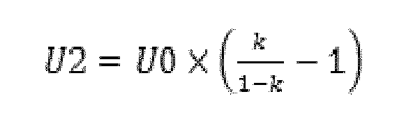
![]()
Die Vorwiderstände R1 und R2 lassen sich nun bei geforderten Kurzschlussstromes Ik zu: 


Mit dieser Dimensionierung ist die Diode D unter Vernachlässigung der relativ geringen Schwellspannung leitend, wenn der Lastwiderstand RL größer als U0/Ik ist, und sie sperrt wenn der Wert kleiner als U0/Ik wird. Die Diode D schaltet somit die nichtlineare Strom-Spannungskennlinie am Punkt MPP maximaler Leistung.With this dimensioning, the diode D, ignoring the relatively low threshold voltage, is conductive when the load resistance RL is greater than U 0 / I k , and it turns off when the value becomes smaller than U 0 / I k . The diode D thus switches the nonlinear current-voltage characteristic at the point MPP of maximum power.
Durch Verwendung einer Diode als Schaltelement D kann auf leistungsbegrenzende aktive Bauelemente, wie z.B. Transistoren verzichtet werden. Dies ermöglicht, höhere Prüfleistungen mit nichtlinearer Charakteristik bereitzustellen.By using a diode as switching element D, it is possible to rely on power limiting active devices, e.g. Transistors are dispensed with. This makes it possible to provide higher test performance with non-linear characteristics.
Die Beanspruchung der Umschaltdiode D hinsichtlich Sperrspannung und Strom liegt im Bereich heute üblicher Werte für Leistungsdioden. So ist die auftretende Sperrspannung immer kleiner als die Leerlaufspannung (Prüfspannung) von z.B. max. 1575 V. Zudem ist der durch die Diode D fließende Strom ebenfalls immer kleiner als der Kurzschlussstrom (Prüfstrom) Ik.The load on the switching diode D with regard to blocking voltage and current is in the range of current values for power diodes today. Thus, the occurring reverse voltage is always smaller than the open circuit voltage (test voltage) of eg max. 1575 V. In addition, the current flowing through the diode D is also always smaller than the short-circuit current (test current) I k .
Die vorliegende Erfindung wurde anhand von Ausführungsbeispielen erläutert. Diese Ausführungsbeispiele sollten keinesfalls als einschränkend für die vorliegende Erfindung verstanden werden.The present invention has been explained with reference to exemplary embodiments. These embodiments should by no means be construed as limiting the present invention.
Claims (10)
Applications Claiming Priority (1)
| Application Number | Priority Date | Filing Date | Title |
|---|---|---|---|
| DE102012103456.7A DE102012103456B4 (en) | 2012-04-19 | 2012-04-19 | Device for outputting a DC voltage signal with non-linear current-voltage characteristic |
Publications (2)
| Publication Number | Publication Date |
|---|---|
| EP2653879A1 true EP2653879A1 (en) | 2013-10-23 |
| EP2653879B1 EP2653879B1 (en) | 2017-08-23 |
Family
ID=48044675
Family Applications (1)
| Application Number | Title | Priority Date | Filing Date |
|---|---|---|---|
| EP13162207.8A Not-in-force EP2653879B1 (en) | 2012-04-19 | 2013-04-03 | Device for the simultaneous output of a direct voltage signal with a non-linear power-voltage curve |
Country Status (2)
| Country | Link |
|---|---|
| EP (1) | EP2653879B1 (en) |
| DE (1) | DE102012103456B4 (en) |
Cited By (1)
| Publication number | Priority date | Publication date | Assignee | Title |
|---|---|---|---|---|
| CN111679713A (en) * | 2020-06-28 | 2020-09-18 | 齐鲁工业大学 | Photovoltaic maximum power point tracking method for direct calculation |
Citations (7)
| Publication number | Priority date | Publication date | Assignee | Title |
|---|---|---|---|---|
| DE2018181A1 (en) * | 1970-04-16 | 1971-11-04 | Messerschmitt Boelkow Blohm | Circuit arrangement for simulating the electrical properties of a solar cell |
| DE2052251B2 (en) * | 1970-10-24 | 1972-05-25 | Licenfia Patent-Verwaltungs-GmbH, 6000 Frankfurt | CIRCUIT ARRANGEMENT FOR REPLACING A SOLAR CELL CHARACTERISTIC CURVE WITH THE HELP OF A FIELD EFFECT TRANSISTOR |
| DE2233612A1 (en) * | 1972-07-07 | 1974-01-31 | Siemens Ag | TEST SIGNALS |
| GB1457654A (en) * | 1973-04-14 | 1976-12-08 | Licentia Gmbh | Circuit for simulation of a solar cell generator having a non- linear current voltage characteristic |
| JPH07234716A (en) * | 1994-02-24 | 1995-09-05 | Toshiba Corp | Solar power generation simulation device |
| KR20090046438A (en) * | 2007-11-06 | 2009-05-11 | 한국전기연구원 | Apparatus and control method for simulation of photovoltaic array |
| US20090133735A1 (en) * | 2006-04-26 | 2009-05-28 | Sansha Electric Manufacturing Co., Ltd. | Solar photovoltaic power generation artificial-power generating method and solar photovoltaic power generation simulator power-supply apparatus |
-
2012
- 2012-04-19 DE DE102012103456.7A patent/DE102012103456B4/en not_active Expired - Fee Related
-
2013
- 2013-04-03 EP EP13162207.8A patent/EP2653879B1/en not_active Not-in-force
Patent Citations (7)
| Publication number | Priority date | Publication date | Assignee | Title |
|---|---|---|---|---|
| DE2018181A1 (en) * | 1970-04-16 | 1971-11-04 | Messerschmitt Boelkow Blohm | Circuit arrangement for simulating the electrical properties of a solar cell |
| DE2052251B2 (en) * | 1970-10-24 | 1972-05-25 | Licenfia Patent-Verwaltungs-GmbH, 6000 Frankfurt | CIRCUIT ARRANGEMENT FOR REPLACING A SOLAR CELL CHARACTERISTIC CURVE WITH THE HELP OF A FIELD EFFECT TRANSISTOR |
| DE2233612A1 (en) * | 1972-07-07 | 1974-01-31 | Siemens Ag | TEST SIGNALS |
| GB1457654A (en) * | 1973-04-14 | 1976-12-08 | Licentia Gmbh | Circuit for simulation of a solar cell generator having a non- linear current voltage characteristic |
| JPH07234716A (en) * | 1994-02-24 | 1995-09-05 | Toshiba Corp | Solar power generation simulation device |
| US20090133735A1 (en) * | 2006-04-26 | 2009-05-28 | Sansha Electric Manufacturing Co., Ltd. | Solar photovoltaic power generation artificial-power generating method and solar photovoltaic power generation simulator power-supply apparatus |
| KR20090046438A (en) * | 2007-11-06 | 2009-05-11 | 한국전기연구원 | Apparatus and control method for simulation of photovoltaic array |
Non-Patent Citations (1)
| Title |
|---|
| HEINRICH HÄBERLIN: "Bau eines Solargenerator-Simulators von 100 kW", 23. SYMPOSIUM PHOTOVOLTAISCHE SOLARENERGIE STAFFELSTEIN 2008, 7 March 2008 (2008-03-07), Staffelstein, XP002699927, Retrieved from the Internet <URL:http://www.pvtest.ch/fileadmin/user_upload/lab1/pv/publikationen/SIM-100-Beitrag-K_F.pdf> [retrieved on 20130704] * |
Cited By (1)
| Publication number | Priority date | Publication date | Assignee | Title |
|---|---|---|---|---|
| CN111679713A (en) * | 2020-06-28 | 2020-09-18 | 齐鲁工业大学 | Photovoltaic maximum power point tracking method for direct calculation |
Also Published As
| Publication number | Publication date |
|---|---|
| DE102012103456A1 (en) | 2013-10-24 |
| EP2653879B1 (en) | 2017-08-23 |
| DE102012103456B4 (en) | 2014-09-04 |
Similar Documents
| Publication | Publication Date | Title |
|---|---|---|
| EP1857825B1 (en) | Measuring apparatus | |
| EP2700962B1 (en) | Measurement of a resistance of a switch contact of an electrical circuit breaker | |
| EP2418748B1 (en) | Energy supply device | |
| DE102013207775B4 (en) | Device for detecting a fault in an electrical line | |
| EP2157437A1 (en) | Method for measuring a current, particularly through an earthing device | |
| EP2523294B1 (en) | Switching assembly for a protection device for electrical assemblies | |
| DE69811950T2 (en) | ELECTRONIC MONITORING CIRCUIT FOR ELECTRICAL VOLTAGE | |
| EP2856184A1 (en) | Device for testing an electric component | |
| DE102016117003A1 (en) | Protection device | |
| EP1816483B1 (en) | Short-circuit and overcurrent detection circuit | |
| DE102020114018A1 (en) | Method and device for determining the direction to an earth fault | |
| DE102013202868C5 (en) | Fault and / or load detection device for a low or high voltage system | |
| EP2653879B1 (en) | Device for the simultaneous output of a direct voltage signal with a non-linear power-voltage curve | |
| AT516121B1 (en) | Checking a multi-pole electrical circuit breaker | |
| EP3417300B1 (en) | Testing device and method for testing a control unit of a switching device of a switchgear installation | |
| EP3652860B1 (en) | Level converter and a method for converting level values in vehicle control devices | |
| DE102020131512A1 (en) | Device for generating a compensation current | |
| DE102016120099B3 (en) | Energy supply unit for providing at least one switchable energy output | |
| DE19912410A1 (en) | Measuring method for a high-voltage bushing and suitable measuring arrangement | |
| DE19518729A1 (en) | Battery cell parameter measuring device | |
| DE2456073B2 (en) | PROTECTIVE ARRANGEMENT FOR THREE-PHASE TRANSMISSION SYSTEMS | |
| EP0171563B1 (en) | Circuit for the testing under load of a low-voltage current source | |
| AT514280B1 (en) | Cable tester and method for testing an n-pole cable | |
| DE102012004944B4 (en) | Method for checking the function of electrical connections of an analog or digital circuit | |
| EP4113129A1 (en) | Method for measuring the current through a shunt resistor |
Legal Events
| Date | Code | Title | Description |
|---|---|---|---|
| PUAI | Public reference made under article 153(3) epc to a published international application that has entered the european phase |
Free format text: ORIGINAL CODE: 0009012 |
|
| AK | Designated contracting states |
Kind code of ref document: A1 Designated state(s): AL AT BE BG CH CY CZ DE DK EE ES FI FR GB GR HR HU IE IS IT LI LT LU LV MC MK MT NL NO PL PT RO RS SE SI SK SM TR |
|
| AX | Request for extension of the european patent |
Extension state: BA ME |
|
| 17P | Request for examination filed |
Effective date: 20140411 |
|
| RBV | Designated contracting states (corrected) |
Designated state(s): AL AT BE BG CH CY CZ DE DK EE ES FI FR GB GR HR HU IE IS IT LI LT LU LV MC MK MT NL NO PL PT RO RS SE SI SK SM TR |
|
| REG | Reference to a national code |
Ref country code: DE Ref legal event code: R079 Ref document number: 502013008118 Country of ref document: DE Free format text: PREVIOUS MAIN CLASS: G01R0031280000 Ipc: H02S0050100000 |
|
| GRAP | Despatch of communication of intention to grant a patent |
Free format text: ORIGINAL CODE: EPIDOSNIGR1 |
|
| INTG | Intention to grant announced |
Effective date: 20170323 |
|
| RIC1 | Information provided on ipc code assigned before grant |
Ipc: G01R 31/28 20060101ALI20170313BHEP Ipc: G01R 31/40 20140101ALI20170313BHEP Ipc: H02S 50/10 20140101AFI20170313BHEP |
|
| GRAS | Grant fee paid |
Free format text: ORIGINAL CODE: EPIDOSNIGR3 |
|
| GRAA | (expected) grant |
Free format text: ORIGINAL CODE: 0009210 |
|
| AK | Designated contracting states |
Kind code of ref document: B1 Designated state(s): AL AT BE BG CH CY CZ DE DK EE ES FI FR GB GR HR HU IE IS IT LI LT LU LV MC MK MT NL NO PL PT RO RS SE SI SK SM TR |
|
| REG | Reference to a national code |
Ref country code: GB Ref legal event code: FG4D Free format text: NOT ENGLISH |
|
| REG | Reference to a national code |
Ref country code: CH Ref legal event code: EP |
|
| REG | Reference to a national code |
Ref country code: AT Ref legal event code: REF Ref document number: 922320 Country of ref document: AT Kind code of ref document: T Effective date: 20170915 |
|
| REG | Reference to a national code |
Ref country code: IE Ref legal event code: FG4D Free format text: LANGUAGE OF EP DOCUMENT: GERMAN |
|
| REG | Reference to a national code |
Ref country code: DE Ref legal event code: R096 Ref document number: 502013008118 Country of ref document: DE |
|
| REG | Reference to a national code |
Ref country code: SE Ref legal event code: TRGR |
|
| REG | Reference to a national code |
Ref country code: NL Ref legal event code: FP |
|
| REG | Reference to a national code |
Ref country code: LT Ref legal event code: MG4D |
|
| PG25 | Lapsed in a contracting state [announced via postgrant information from national office to epo] |
Ref country code: NO Free format text: LAPSE BECAUSE OF FAILURE TO SUBMIT A TRANSLATION OF THE DESCRIPTION OR TO PAY THE FEE WITHIN THE PRESCRIBED TIME-LIMIT Effective date: 20171123 Ref country code: LT Free format text: LAPSE BECAUSE OF FAILURE TO SUBMIT A TRANSLATION OF THE DESCRIPTION OR TO PAY THE FEE WITHIN THE PRESCRIBED TIME-LIMIT Effective date: 20170823 Ref country code: HR Free format text: LAPSE BECAUSE OF FAILURE TO SUBMIT A TRANSLATION OF THE DESCRIPTION OR TO PAY THE FEE WITHIN THE PRESCRIBED TIME-LIMIT Effective date: 20170823 Ref country code: FI Free format text: LAPSE BECAUSE OF FAILURE TO SUBMIT A TRANSLATION OF THE DESCRIPTION OR TO PAY THE FEE WITHIN THE PRESCRIBED TIME-LIMIT Effective date: 20170823 |
|
| PG25 | Lapsed in a contracting state [announced via postgrant information from national office to epo] |
Ref country code: IS Free format text: LAPSE BECAUSE OF FAILURE TO SUBMIT A TRANSLATION OF THE DESCRIPTION OR TO PAY THE FEE WITHIN THE PRESCRIBED TIME-LIMIT Effective date: 20171223 Ref country code: GR Free format text: LAPSE BECAUSE OF FAILURE TO SUBMIT A TRANSLATION OF THE DESCRIPTION OR TO PAY THE FEE WITHIN THE PRESCRIBED TIME-LIMIT Effective date: 20171124 Ref country code: ES Free format text: LAPSE BECAUSE OF FAILURE TO SUBMIT A TRANSLATION OF THE DESCRIPTION OR TO PAY THE FEE WITHIN THE PRESCRIBED TIME-LIMIT Effective date: 20170823 Ref country code: PL Free format text: LAPSE BECAUSE OF FAILURE TO SUBMIT A TRANSLATION OF THE DESCRIPTION OR TO PAY THE FEE WITHIN THE PRESCRIBED TIME-LIMIT Effective date: 20170823 Ref country code: LV Free format text: LAPSE BECAUSE OF FAILURE TO SUBMIT A TRANSLATION OF THE DESCRIPTION OR TO PAY THE FEE WITHIN THE PRESCRIBED TIME-LIMIT Effective date: 20170823 Ref country code: BG Free format text: LAPSE BECAUSE OF FAILURE TO SUBMIT A TRANSLATION OF THE DESCRIPTION OR TO PAY THE FEE WITHIN THE PRESCRIBED TIME-LIMIT Effective date: 20171123 Ref country code: RS Free format text: LAPSE BECAUSE OF FAILURE TO SUBMIT A TRANSLATION OF THE DESCRIPTION OR TO PAY THE FEE WITHIN THE PRESCRIBED TIME-LIMIT Effective date: 20170823 |
|
| REG | Reference to a national code |
Ref country code: FR Ref legal event code: PLFP Year of fee payment: 6 |
|
| PG25 | Lapsed in a contracting state [announced via postgrant information from national office to epo] |
Ref country code: RO Free format text: LAPSE BECAUSE OF FAILURE TO SUBMIT A TRANSLATION OF THE DESCRIPTION OR TO PAY THE FEE WITHIN THE PRESCRIBED TIME-LIMIT Effective date: 20170823 Ref country code: DK Free format text: LAPSE BECAUSE OF FAILURE TO SUBMIT A TRANSLATION OF THE DESCRIPTION OR TO PAY THE FEE WITHIN THE PRESCRIBED TIME-LIMIT Effective date: 20170823 |
|
| REG | Reference to a national code |
Ref country code: DE Ref legal event code: R097 Ref document number: 502013008118 Country of ref document: DE |
|
| PG25 | Lapsed in a contracting state [announced via postgrant information from national office to epo] |
Ref country code: SK Free format text: LAPSE BECAUSE OF FAILURE TO SUBMIT A TRANSLATION OF THE DESCRIPTION OR TO PAY THE FEE WITHIN THE PRESCRIBED TIME-LIMIT Effective date: 20170823 Ref country code: EE Free format text: LAPSE BECAUSE OF FAILURE TO SUBMIT A TRANSLATION OF THE DESCRIPTION OR TO PAY THE FEE WITHIN THE PRESCRIBED TIME-LIMIT Effective date: 20170823 Ref country code: SM Free format text: LAPSE BECAUSE OF FAILURE TO SUBMIT A TRANSLATION OF THE DESCRIPTION OR TO PAY THE FEE WITHIN THE PRESCRIBED TIME-LIMIT Effective date: 20170823 |
|
| PLBE | No opposition filed within time limit |
Free format text: ORIGINAL CODE: 0009261 |
|
| STAA | Information on the status of an ep patent application or granted ep patent |
Free format text: STATUS: NO OPPOSITION FILED WITHIN TIME LIMIT |
|
| 26N | No opposition filed |
Effective date: 20180524 |
|
| PG25 | Lapsed in a contracting state [announced via postgrant information from national office to epo] |
Ref country code: SI Free format text: LAPSE BECAUSE OF FAILURE TO SUBMIT A TRANSLATION OF THE DESCRIPTION OR TO PAY THE FEE WITHIN THE PRESCRIBED TIME-LIMIT Effective date: 20170823 |
|
| PG25 | Lapsed in a contracting state [announced via postgrant information from national office to epo] |
Ref country code: MT Free format text: LAPSE BECAUSE OF FAILURE TO SUBMIT A TRANSLATION OF THE DESCRIPTION OR TO PAY THE FEE WITHIN THE PRESCRIBED TIME-LIMIT Effective date: 20170823 |
|
| PG25 | Lapsed in a contracting state [announced via postgrant information from national office to epo] |
Ref country code: MC Free format text: LAPSE BECAUSE OF FAILURE TO SUBMIT A TRANSLATION OF THE DESCRIPTION OR TO PAY THE FEE WITHIN THE PRESCRIBED TIME-LIMIT Effective date: 20170823 |
|
| REG | Reference to a national code |
Ref country code: CH Ref legal event code: PL |
|
| REG | Reference to a national code |
Ref country code: BE Ref legal event code: MM Effective date: 20180430 |
|
| REG | Reference to a national code |
Ref country code: IE Ref legal event code: MM4A |
|
| PG25 | Lapsed in a contracting state [announced via postgrant information from national office to epo] |
Ref country code: LU Free format text: LAPSE BECAUSE OF NON-PAYMENT OF DUE FEES Effective date: 20180403 |
|
| PG25 | Lapsed in a contracting state [announced via postgrant information from national office to epo] |
Ref country code: LI Free format text: LAPSE BECAUSE OF NON-PAYMENT OF DUE FEES Effective date: 20180430 Ref country code: CH Free format text: LAPSE BECAUSE OF NON-PAYMENT OF DUE FEES Effective date: 20180430 Ref country code: BE Free format text: LAPSE BECAUSE OF NON-PAYMENT OF DUE FEES Effective date: 20180430 |
|
| PG25 | Lapsed in a contracting state [announced via postgrant information from national office to epo] |
Ref country code: IE Free format text: LAPSE BECAUSE OF NON-PAYMENT OF DUE FEES Effective date: 20180403 |
|
| REG | Reference to a national code |
Ref country code: AT Ref legal event code: MM01 Ref document number: 922320 Country of ref document: AT Kind code of ref document: T Effective date: 20180403 |
|
| PG25 | Lapsed in a contracting state [announced via postgrant information from national office to epo] |
Ref country code: AT Free format text: LAPSE BECAUSE OF NON-PAYMENT OF DUE FEES Effective date: 20180403 |
|
| PG25 | Lapsed in a contracting state [announced via postgrant information from national office to epo] |
Ref country code: TR Free format text: LAPSE BECAUSE OF FAILURE TO SUBMIT A TRANSLATION OF THE DESCRIPTION OR TO PAY THE FEE WITHIN THE PRESCRIBED TIME-LIMIT Effective date: 20170823 |
|
| PG25 | Lapsed in a contracting state [announced via postgrant information from national office to epo] |
Ref country code: PT Free format text: LAPSE BECAUSE OF FAILURE TO SUBMIT A TRANSLATION OF THE DESCRIPTION OR TO PAY THE FEE WITHIN THE PRESCRIBED TIME-LIMIT Effective date: 20170823 Ref country code: HU Free format text: LAPSE BECAUSE OF FAILURE TO SUBMIT A TRANSLATION OF THE DESCRIPTION OR TO PAY THE FEE WITHIN THE PRESCRIBED TIME-LIMIT; INVALID AB INITIO Effective date: 20130403 |
|
| PG25 | Lapsed in a contracting state [announced via postgrant information from national office to epo] |
Ref country code: MK Free format text: LAPSE BECAUSE OF NON-PAYMENT OF DUE FEES Effective date: 20170823 Ref country code: CY Free format text: LAPSE BECAUSE OF FAILURE TO SUBMIT A TRANSLATION OF THE DESCRIPTION OR TO PAY THE FEE WITHIN THE PRESCRIBED TIME-LIMIT Effective date: 20170823 |
|
| PG25 | Lapsed in a contracting state [announced via postgrant information from national office to epo] |
Ref country code: AL Free format text: LAPSE BECAUSE OF FAILURE TO SUBMIT A TRANSLATION OF THE DESCRIPTION OR TO PAY THE FEE WITHIN THE PRESCRIBED TIME-LIMIT Effective date: 20170823 |
|
| PGFP | Annual fee paid to national office [announced via postgrant information from national office to epo] |
Ref country code: NL Payment date: 20220420 Year of fee payment: 10 |
|
| PGFP | Annual fee paid to national office [announced via postgrant information from national office to epo] |
Ref country code: SE Payment date: 20220421 Year of fee payment: 10 Ref country code: IT Payment date: 20220420 Year of fee payment: 10 Ref country code: GB Payment date: 20220425 Year of fee payment: 10 Ref country code: FR Payment date: 20220421 Year of fee payment: 10 Ref country code: DE Payment date: 20220222 Year of fee payment: 10 Ref country code: CZ Payment date: 20220404 Year of fee payment: 10 |
|
| PG25 | Lapsed in a contracting state [announced via postgrant information from national office to epo] |
Ref country code: CZ Free format text: LAPSE BECAUSE OF NON-PAYMENT OF DUE FEES Effective date: 20230403 |
|
| REG | Reference to a national code |
Ref country code: DE Ref legal event code: R119 Ref document number: 502013008118 Country of ref document: DE |
|
| REG | Reference to a national code |
Ref country code: SE Ref legal event code: EUG |
|
| REG | Reference to a national code |
Ref country code: NL Ref legal event code: MM Effective date: 20230501 |
|
| GBPC | Gb: european patent ceased through non-payment of renewal fee |
Effective date: 20230403 |
|
| PG25 | Lapsed in a contracting state [announced via postgrant information from national office to epo] |
Ref country code: GB Free format text: LAPSE BECAUSE OF NON-PAYMENT OF DUE FEES Effective date: 20230403 |
|
| PG25 | Lapsed in a contracting state [announced via postgrant information from national office to epo] |
Ref country code: SE Free format text: LAPSE BECAUSE OF NON-PAYMENT OF DUE FEES Effective date: 20230404 Ref country code: NL Free format text: LAPSE BECAUSE OF NON-PAYMENT OF DUE FEES Effective date: 20230501 Ref country code: GB Free format text: LAPSE BECAUSE OF NON-PAYMENT OF DUE FEES Effective date: 20230403 Ref country code: FR Free format text: LAPSE BECAUSE OF NON-PAYMENT OF DUE FEES Effective date: 20230430 Ref country code: DE Free format text: LAPSE BECAUSE OF NON-PAYMENT OF DUE FEES Effective date: 20231103 |
|
| PG25 | Lapsed in a contracting state [announced via postgrant information from national office to epo] |
Ref country code: IT Free format text: LAPSE BECAUSE OF NON-PAYMENT OF DUE FEES Effective date: 20230403 |