EP2652548B1 - Dispositif electrochrome tout-solide, bicouche electrochrome pour ce dispositif, et procede de preparation de ce dispositif. - Google Patents
Dispositif electrochrome tout-solide, bicouche electrochrome pour ce dispositif, et procede de preparation de ce dispositif. Download PDFInfo
- Publication number
- EP2652548B1 EP2652548B1 EP11794759.8A EP11794759A EP2652548B1 EP 2652548 B1 EP2652548 B1 EP 2652548B1 EP 11794759 A EP11794759 A EP 11794759A EP 2652548 B1 EP2652548 B1 EP 2652548B1
- Authority
- EP
- European Patent Office
- Prior art keywords
- layer
- electron
- proton
- electrochromic
- tungsten oxide
- Prior art date
- Legal status (The legal status is an assumption and is not a legal conclusion. Google has not performed a legal analysis and makes no representation as to the accuracy of the status listed.)
- Active
Links
- 238000004519 manufacturing process Methods 0.000 title description 3
- 239000010410 layer Substances 0.000 claims description 184
- 239000000463 material Substances 0.000 claims description 95
- QGLKJKCYBOYXKC-UHFFFAOYSA-N nonaoxidotritungsten Chemical compound O=[W]1(=O)O[W](=O)(=O)O[W](=O)(=O)O1 QGLKJKCYBOYXKC-UHFFFAOYSA-N 0.000 claims description 61
- 229910001930 tungsten oxide Inorganic materials 0.000 claims description 61
- 239000000758 substrate Substances 0.000 claims description 49
- 239000004020 conductor Substances 0.000 claims description 46
- 239000003792 electrolyte Substances 0.000 claims description 36
- 238000000034 method Methods 0.000 claims description 27
- 229910052751 metal Inorganic materials 0.000 claims description 23
- 239000002184 metal Substances 0.000 claims description 23
- 239000007787 solid Substances 0.000 claims description 22
- 238000009830 intercalation Methods 0.000 claims description 21
- 230000002687 intercalation Effects 0.000 claims description 21
- 230000005855 radiation Effects 0.000 claims description 19
- 239000011521 glass Substances 0.000 claims description 18
- 239000000203 mixture Substances 0.000 claims description 17
- 229910044991 metal oxide Inorganic materials 0.000 claims description 16
- 150000004706 metal oxides Chemical class 0.000 claims description 16
- 238000003860 storage Methods 0.000 claims description 16
- 238000005240 physical vapour deposition Methods 0.000 claims description 13
- 239000002250 absorbent Substances 0.000 claims description 11
- 230000002745 absorbent Effects 0.000 claims description 11
- 150000002739 metals Chemical class 0.000 claims description 11
- BASFCYQUMIYNBI-UHFFFAOYSA-N platinum Chemical compound [Pt] BASFCYQUMIYNBI-UHFFFAOYSA-N 0.000 claims description 10
- 239000011241 protective layer Substances 0.000 claims description 10
- 238000004544 sputter deposition Methods 0.000 claims description 10
- 229910010272 inorganic material Inorganic materials 0.000 claims description 8
- 239000011147 inorganic material Substances 0.000 claims description 8
- 229910052752 metalloid Inorganic materials 0.000 claims description 8
- 150000002738 metalloids Chemical class 0.000 claims description 8
- 229920000139 polyethylene terephthalate Polymers 0.000 claims description 8
- 239000005020 polyethylene terephthalate Substances 0.000 claims description 8
- VYPSYNLAJGMNEJ-UHFFFAOYSA-N Silicium dioxide Chemical compound O=[Si]=O VYPSYNLAJGMNEJ-UHFFFAOYSA-N 0.000 claims description 6
- 239000000126 substance Substances 0.000 claims description 6
- VYZAMTAEIAYCRO-UHFFFAOYSA-N Chromium Chemical compound [Cr] VYZAMTAEIAYCRO-UHFFFAOYSA-N 0.000 claims description 5
- 229910045601 alloy Inorganic materials 0.000 claims description 5
- 239000000956 alloy Substances 0.000 claims description 5
- 229910052782 aluminium Inorganic materials 0.000 claims description 5
- XAGFODPZIPBFFR-UHFFFAOYSA-N aluminium Chemical compound [Al] XAGFODPZIPBFFR-UHFFFAOYSA-N 0.000 claims description 5
- 229910052804 chromium Inorganic materials 0.000 claims description 5
- 239000011651 chromium Substances 0.000 claims description 5
- 238000001704 evaporation Methods 0.000 claims description 5
- 230000008020 evaporation Effects 0.000 claims description 5
- 238000000608 laser ablation Methods 0.000 claims description 5
- 229910052697 platinum Inorganic materials 0.000 claims description 5
- XOLBLPGZBRYERU-UHFFFAOYSA-N tin dioxide Chemical compound O=[Sn]=O XOLBLPGZBRYERU-UHFFFAOYSA-N 0.000 claims description 5
- 229910001887 tin oxide Inorganic materials 0.000 claims description 5
- 229920000620 organic polymer Polymers 0.000 claims description 4
- -1 polyethylene terephthalate Polymers 0.000 claims description 4
- 231100000252 nontoxic Toxicity 0.000 claims description 3
- 230000003000 nontoxic effect Effects 0.000 claims description 3
- SIWVEOZUMHYXCS-UHFFFAOYSA-N oxo(oxoyttriooxy)yttrium Chemical compound O=[Y]O[Y]=O SIWVEOZUMHYXCS-UHFFFAOYSA-N 0.000 claims description 3
- RVTZCBVAJQQJTK-UHFFFAOYSA-N oxygen(2-);zirconium(4+) Chemical compound [O-2].[O-2].[Zr+4] RVTZCBVAJQQJTK-UHFFFAOYSA-N 0.000 claims description 3
- 239000000377 silicon dioxide Substances 0.000 claims description 3
- 229910001936 tantalum oxide Inorganic materials 0.000 claims description 3
- 238000001947 vapour-phase growth Methods 0.000 claims description 3
- 229910001928 zirconium oxide Inorganic materials 0.000 claims description 3
- 229910000420 cerium oxide Inorganic materials 0.000 claims description 2
- AMGQUBHHOARCQH-UHFFFAOYSA-N indium;oxotin Chemical compound [In].[Sn]=O AMGQUBHHOARCQH-UHFFFAOYSA-N 0.000 claims description 2
- BMMGVYCKOGBVEV-UHFFFAOYSA-N oxo(oxoceriooxy)cerium Chemical compound [Ce]=O.O=[Ce]=O BMMGVYCKOGBVEV-UHFFFAOYSA-N 0.000 claims description 2
- VVRQVWSVLMGPRN-UHFFFAOYSA-N oxotungsten Chemical class [W]=O VVRQVWSVLMGPRN-UHFFFAOYSA-N 0.000 claims description 2
- BPUBBGLMJRNUCC-UHFFFAOYSA-N oxygen(2-);tantalum(5+) Chemical compound [O-2].[O-2].[O-2].[O-2].[O-2].[Ta+5].[Ta+5] BPUBBGLMJRNUCC-UHFFFAOYSA-N 0.000 claims description 2
- 239000004411 aluminium Substances 0.000 claims 2
- CETPSERCERDGAM-UHFFFAOYSA-N ceric oxide Chemical compound O=[Ce]=O CETPSERCERDGAM-UHFFFAOYSA-N 0.000 claims 1
- 229910000422 cerium(IV) oxide Inorganic materials 0.000 claims 1
- 239000011248 coating agent Substances 0.000 claims 1
- 238000000576 coating method Methods 0.000 claims 1
- 229910052681 coesite Inorganic materials 0.000 claims 1
- 229910052906 cristobalite Inorganic materials 0.000 claims 1
- 229910052682 stishovite Inorganic materials 0.000 claims 1
- PBCFLUZVCVVTBY-UHFFFAOYSA-N tantalum pentoxide Inorganic materials O=[Ta](=O)O[Ta](=O)=O PBCFLUZVCVVTBY-UHFFFAOYSA-N 0.000 claims 1
- 229910052905 tridymite Inorganic materials 0.000 claims 1
- 239000011149 active material Substances 0.000 description 27
- 230000003287 optical effect Effects 0.000 description 27
- 238000000151 deposition Methods 0.000 description 20
- 239000011232 storage material Substances 0.000 description 20
- XKRFYHLGVUSROY-UHFFFAOYSA-N Argon Chemical compound [Ar] XKRFYHLGVUSROY-UHFFFAOYSA-N 0.000 description 14
- QVGXLLKOCUKJST-UHFFFAOYSA-N atomic oxygen Chemical compound [O] QVGXLLKOCUKJST-UHFFFAOYSA-N 0.000 description 14
- 239000001301 oxygen Substances 0.000 description 14
- 229910052760 oxygen Inorganic materials 0.000 description 14
- 230000008021 deposition Effects 0.000 description 13
- WFKWXMTUELFFGS-UHFFFAOYSA-N tungsten Chemical compound [W] WFKWXMTUELFFGS-UHFFFAOYSA-N 0.000 description 11
- 229910052721 tungsten Inorganic materials 0.000 description 11
- 229910052737 gold Inorganic materials 0.000 description 10
- 239000010931 gold Substances 0.000 description 10
- PCHJSUWPFVWCPO-UHFFFAOYSA-N gold Chemical compound [Au] PCHJSUWPFVWCPO-UHFFFAOYSA-N 0.000 description 9
- 150000002500 ions Chemical class 0.000 description 9
- 230000008569 process Effects 0.000 description 9
- 239000010937 tungsten Substances 0.000 description 9
- 239000002131 composite material Substances 0.000 description 8
- 230000006870 function Effects 0.000 description 8
- 238000001755 magnetron sputter deposition Methods 0.000 description 8
- 229910052786 argon Inorganic materials 0.000 description 7
- 229910052739 hydrogen Inorganic materials 0.000 description 7
- 230000008901 benefit Effects 0.000 description 6
- 230000004044 response Effects 0.000 description 6
- 238000013461 design Methods 0.000 description 5
- 230000002829 reductive effect Effects 0.000 description 5
- 239000011195 cermet Substances 0.000 description 4
- 239000007789 gas Substances 0.000 description 4
- 238000003780 insertion Methods 0.000 description 4
- 230000037431 insertion Effects 0.000 description 4
- 229910001416 lithium ion Inorganic materials 0.000 description 4
- 229910052715 tantalum Inorganic materials 0.000 description 4
- GUVRBAGPIYLISA-UHFFFAOYSA-N tantalum atom Chemical compound [Ta] GUVRBAGPIYLISA-UHFFFAOYSA-N 0.000 description 4
- IJGRMHOSHXDMSA-UHFFFAOYSA-N Atomic nitrogen Chemical compound N#N IJGRMHOSHXDMSA-UHFFFAOYSA-N 0.000 description 3
- HBBGRARXTFLTSG-UHFFFAOYSA-N Lithium ion Chemical compound [Li+] HBBGRARXTFLTSG-UHFFFAOYSA-N 0.000 description 3
- 238000009792 diffusion process Methods 0.000 description 3
- 230000000694 effects Effects 0.000 description 3
- 229910052741 iridium Inorganic materials 0.000 description 3
- 229920000642 polymer Polymers 0.000 description 3
- 229920000297 Rayon Polymers 0.000 description 2
- 229910004298 SiO 2 Inorganic materials 0.000 description 2
- 238000010521 absorption reaction Methods 0.000 description 2
- 238000002425 crystallisation Methods 0.000 description 2
- 230000008025 crystallization Effects 0.000 description 2
- 239000012776 electronic material Substances 0.000 description 2
- 238000010438 heat treatment Methods 0.000 description 2
- 229910003437 indium oxide Inorganic materials 0.000 description 2
- PJXISJQVUVHSOJ-UHFFFAOYSA-N indium(iii) oxide Chemical compound [O-2].[O-2].[O-2].[In+3].[In+3] PJXISJQVUVHSOJ-UHFFFAOYSA-N 0.000 description 2
- 239000012212 insulator Substances 0.000 description 2
- 230000000670 limiting effect Effects 0.000 description 2
- 239000007788 liquid Substances 0.000 description 2
- 239000011244 liquid electrolyte Substances 0.000 description 2
- 239000012811 non-conductive material Substances 0.000 description 2
- CXKGGJDGRUUNKU-UHFFFAOYSA-N oxotungsten;hydrate Chemical compound O.[W]=O CXKGGJDGRUUNKU-UHFFFAOYSA-N 0.000 description 2
- 229920005569 poly(vinylidene fluoride-co-hexafluoropropylene) Polymers 0.000 description 2
- 239000000843 powder Substances 0.000 description 2
- 239000002964 rayon Substances 0.000 description 2
- 230000002441 reversible effect Effects 0.000 description 2
- 238000001771 vacuum deposition Methods 0.000 description 2
- 206010001488 Aggression Diseases 0.000 description 1
- 229910016036 BaF 2 Inorganic materials 0.000 description 1
- 229910052684 Cerium Inorganic materials 0.000 description 1
- UFHFLCQGNIYNRP-UHFFFAOYSA-N Hydrogen Chemical compound [H][H] UFHFLCQGNIYNRP-UHFFFAOYSA-N 0.000 description 1
- 229910006404 SnO 2 Inorganic materials 0.000 description 1
- 230000002378 acidificating effect Effects 0.000 description 1
- 230000016571 aggressive behavior Effects 0.000 description 1
- 150000001450 anions Chemical class 0.000 description 1
- 230000002238 attenuated effect Effects 0.000 description 1
- 230000015556 catabolic process Effects 0.000 description 1
- 150000001768 cations Chemical class 0.000 description 1
- GWXLDORMOJMVQZ-UHFFFAOYSA-N cerium Chemical compound [Ce] GWXLDORMOJMVQZ-UHFFFAOYSA-N 0.000 description 1
- 239000003153 chemical reaction reagent Substances 0.000 description 1
- 230000000295 complement effect Effects 0.000 description 1
- 150000001875 compounds Chemical class 0.000 description 1
- 229920001940 conductive polymer Polymers 0.000 description 1
- 239000000470 constituent Substances 0.000 description 1
- 230000001276 controlling effect Effects 0.000 description 1
- 230000007547 defect Effects 0.000 description 1
- 238000006731 degradation reaction Methods 0.000 description 1
- HTXDPTMKBJXEOW-UHFFFAOYSA-N dioxoiridium Chemical compound O=[Ir]=O HTXDPTMKBJXEOW-UHFFFAOYSA-N 0.000 description 1
- 238000001035 drying Methods 0.000 description 1
- 239000011532 electronic conductor Substances 0.000 description 1
- 238000005538 encapsulation Methods 0.000 description 1
- 238000005516 engineering process Methods 0.000 description 1
- ZULTVNRFZRQYKL-UHFFFAOYSA-M fluorotin Chemical compound [Sn]F ZULTVNRFZRQYKL-UHFFFAOYSA-M 0.000 description 1
- 239000000499 gel Substances 0.000 description 1
- 239000011245 gel electrolyte Substances 0.000 description 1
- 150000002343 gold Chemical class 0.000 description 1
- 239000001257 hydrogen Substances 0.000 description 1
- 238000005470 impregnation Methods 0.000 description 1
- 229910052738 indium Inorganic materials 0.000 description 1
- APFVFJFRJDLVQX-UHFFFAOYSA-N indium atom Chemical compound [In] APFVFJFRJDLVQX-UHFFFAOYSA-N 0.000 description 1
- RHZWSUVWRRXEJF-UHFFFAOYSA-N indium tin Chemical compound [In].[Sn] RHZWSUVWRRXEJF-UHFFFAOYSA-N 0.000 description 1
- 238000002329 infrared spectrum Methods 0.000 description 1
- 229910052500 inorganic mineral Inorganic materials 0.000 description 1
- 239000011229 interlayer Substances 0.000 description 1
- GKOZUEZYRPOHIO-UHFFFAOYSA-N iridium atom Chemical compound [Ir] GKOZUEZYRPOHIO-UHFFFAOYSA-N 0.000 description 1
- 229910000457 iridium oxide Inorganic materials 0.000 description 1
- 238000003475 lamination Methods 0.000 description 1
- 239000002346 layers by function Substances 0.000 description 1
- 239000011159 matrix material Substances 0.000 description 1
- 230000003446 memory effect Effects 0.000 description 1
- 239000012982 microporous membrane Substances 0.000 description 1
- 239000011707 mineral Substances 0.000 description 1
- 238000002156 mixing Methods 0.000 description 1
- 229910052757 nitrogen Inorganic materials 0.000 description 1
- 238000005325 percolation Methods 0.000 description 1
- 238000000206 photolithography Methods 0.000 description 1
- 229920000767 polyaniline Polymers 0.000 description 1
- 229920005597 polymer membrane Polymers 0.000 description 1
- 229920000307 polymer substrate Polymers 0.000 description 1
- 229920000128 polypyrrole Polymers 0.000 description 1
- 229920000123 polythiophene Polymers 0.000 description 1
- 239000011148 porous material Substances 0.000 description 1
- 239000002243 precursor Substances 0.000 description 1
- 238000002360 preparation method Methods 0.000 description 1
- 230000001737 promoting effect Effects 0.000 description 1
- 239000012078 proton-conducting electrolyte Substances 0.000 description 1
- 238000005086 pumping Methods 0.000 description 1
- 230000009257 reactivity Effects 0.000 description 1
- 230000001105 regulatory effect Effects 0.000 description 1
- 238000011160 research Methods 0.000 description 1
- 239000007784 solid electrolyte Substances 0.000 description 1
- 238000012360 testing method Methods 0.000 description 1
- 239000012815 thermoplastic material Substances 0.000 description 1
- QHGNHLZPVBIIPX-UHFFFAOYSA-N tin(ii) oxide Chemical class [Sn]=O QHGNHLZPVBIIPX-UHFFFAOYSA-N 0.000 description 1
- 238000012546 transfer Methods 0.000 description 1
- 230000007704 transition Effects 0.000 description 1
- AAWZNWVCESLFTD-UHFFFAOYSA-N tungsten;hydrate Chemical compound O.[W] AAWZNWVCESLFTD-UHFFFAOYSA-N 0.000 description 1
- 230000000007 visual effect Effects 0.000 description 1
- 230000004584 weight gain Effects 0.000 description 1
- 235000019786 weight gain Nutrition 0.000 description 1
Images


Classifications
-
- G—PHYSICS
- G02—OPTICS
- G02F—OPTICAL DEVICES OR ARRANGEMENTS FOR THE CONTROL OF LIGHT BY MODIFICATION OF THE OPTICAL PROPERTIES OF THE MEDIA OF THE ELEMENTS INVOLVED THEREIN; NON-LINEAR OPTICS; FREQUENCY-CHANGING OF LIGHT; OPTICAL LOGIC ELEMENTS; OPTICAL ANALOGUE/DIGITAL CONVERTERS
- G02F1/00—Devices or arrangements for the control of the intensity, colour, phase, polarisation or direction of light arriving from an independent light source, e.g. switching, gating or modulating; Non-linear optics
- G02F1/01—Devices or arrangements for the control of the intensity, colour, phase, polarisation or direction of light arriving from an independent light source, e.g. switching, gating or modulating; Non-linear optics for the control of the intensity, phase, polarisation or colour
- G02F1/15—Devices or arrangements for the control of the intensity, colour, phase, polarisation or direction of light arriving from an independent light source, e.g. switching, gating or modulating; Non-linear optics for the control of the intensity, phase, polarisation or colour based on an electrochromic effect
- G02F1/1514—Devices or arrangements for the control of the intensity, colour, phase, polarisation or direction of light arriving from an independent light source, e.g. switching, gating or modulating; Non-linear optics for the control of the intensity, phase, polarisation or colour based on an electrochromic effect characterised by the electrochromic material, e.g. by the electrodeposited material
- G02F1/1523—Devices or arrangements for the control of the intensity, colour, phase, polarisation or direction of light arriving from an independent light source, e.g. switching, gating or modulating; Non-linear optics for the control of the intensity, phase, polarisation or colour based on an electrochromic effect characterised by the electrochromic material, e.g. by the electrodeposited material comprising inorganic material
- G02F1/1524—Transition metal compounds
-
- B—PERFORMING OPERATIONS; TRANSPORTING
- B64—AIRCRAFT; AVIATION; COSMONAUTICS
- B64G—COSMONAUTICS; VEHICLES OR EQUIPMENT THEREFOR
- B64G1/00—Cosmonautic vehicles
- B64G1/22—Parts of, or equipment specially adapted for fitting in or to, cosmonautic vehicles
- B64G1/52—Protection, safety or emergency devices; Survival aids
- B64G1/58—Thermal protection, e.g. heat shields
-
- G—PHYSICS
- G02—OPTICS
- G02F—OPTICAL DEVICES OR ARRANGEMENTS FOR THE CONTROL OF LIGHT BY MODIFICATION OF THE OPTICAL PROPERTIES OF THE MEDIA OF THE ELEMENTS INVOLVED THEREIN; NON-LINEAR OPTICS; FREQUENCY-CHANGING OF LIGHT; OPTICAL LOGIC ELEMENTS; OPTICAL ANALOGUE/DIGITAL CONVERTERS
- G02F1/00—Devices or arrangements for the control of the intensity, colour, phase, polarisation or direction of light arriving from an independent light source, e.g. switching, gating or modulating; Non-linear optics
- G02F1/01—Devices or arrangements for the control of the intensity, colour, phase, polarisation or direction of light arriving from an independent light source, e.g. switching, gating or modulating; Non-linear optics for the control of the intensity, phase, polarisation or colour
- G02F1/15—Devices or arrangements for the control of the intensity, colour, phase, polarisation or direction of light arriving from an independent light source, e.g. switching, gating or modulating; Non-linear optics for the control of the intensity, phase, polarisation or colour based on an electrochromic effect
- G02F1/1514—Devices or arrangements for the control of the intensity, colour, phase, polarisation or direction of light arriving from an independent light source, e.g. switching, gating or modulating; Non-linear optics for the control of the intensity, phase, polarisation or colour based on an electrochromic effect characterised by the electrochromic material, e.g. by the electrodeposited material
- G02F1/1523—Devices or arrangements for the control of the intensity, colour, phase, polarisation or direction of light arriving from an independent light source, e.g. switching, gating or modulating; Non-linear optics for the control of the intensity, phase, polarisation or colour based on an electrochromic effect characterised by the electrochromic material, e.g. by the electrodeposited material comprising inorganic material
- G02F1/1525—Devices or arrangements for the control of the intensity, colour, phase, polarisation or direction of light arriving from an independent light source, e.g. switching, gating or modulating; Non-linear optics for the control of the intensity, phase, polarisation or colour based on an electrochromic effect characterised by the electrochromic material, e.g. by the electrodeposited material comprising inorganic material characterised by a particular ion transporting layer, e.g. electrolyte
-
- G—PHYSICS
- G02—OPTICS
- G02F—OPTICAL DEVICES OR ARRANGEMENTS FOR THE CONTROL OF LIGHT BY MODIFICATION OF THE OPTICAL PROPERTIES OF THE MEDIA OF THE ELEMENTS INVOLVED THEREIN; NON-LINEAR OPTICS; FREQUENCY-CHANGING OF LIGHT; OPTICAL LOGIC ELEMENTS; OPTICAL ANALOGUE/DIGITAL CONVERTERS
- G02F1/00—Devices or arrangements for the control of the intensity, colour, phase, polarisation or direction of light arriving from an independent light source, e.g. switching, gating or modulating; Non-linear optics
- G02F1/01—Devices or arrangements for the control of the intensity, colour, phase, polarisation or direction of light arriving from an independent light source, e.g. switching, gating or modulating; Non-linear optics for the control of the intensity, phase, polarisation or colour
- G02F1/15—Devices or arrangements for the control of the intensity, colour, phase, polarisation or direction of light arriving from an independent light source, e.g. switching, gating or modulating; Non-linear optics for the control of the intensity, phase, polarisation or colour based on an electrochromic effect
- G02F1/153—Constructional details
- G02F1/155—Electrodes
-
- G—PHYSICS
- G02—OPTICS
- G02F—OPTICAL DEVICES OR ARRANGEMENTS FOR THE CONTROL OF LIGHT BY MODIFICATION OF THE OPTICAL PROPERTIES OF THE MEDIA OF THE ELEMENTS INVOLVED THEREIN; NON-LINEAR OPTICS; FREQUENCY-CHANGING OF LIGHT; OPTICAL LOGIC ELEMENTS; OPTICAL ANALOGUE/DIGITAL CONVERTERS
- G02F1/00—Devices or arrangements for the control of the intensity, colour, phase, polarisation or direction of light arriving from an independent light source, e.g. switching, gating or modulating; Non-linear optics
- G02F1/01—Devices or arrangements for the control of the intensity, colour, phase, polarisation or direction of light arriving from an independent light source, e.g. switching, gating or modulating; Non-linear optics for the control of the intensity, phase, polarisation or colour
- G02F1/15—Devices or arrangements for the control of the intensity, colour, phase, polarisation or direction of light arriving from an independent light source, e.g. switching, gating or modulating; Non-linear optics for the control of the intensity, phase, polarisation or colour based on an electrochromic effect
- G02F1/153—Constructional details
- G02F1/155—Electrodes
- G02F2001/1552—Inner electrode, e.g. the electrochromic layer being sandwiched between the inner electrode and the support substrate
-
- G—PHYSICS
- G02—OPTICS
- G02F—OPTICAL DEVICES OR ARRANGEMENTS FOR THE CONTROL OF LIGHT BY MODIFICATION OF THE OPTICAL PROPERTIES OF THE MEDIA OF THE ELEMENTS INVOLVED THEREIN; NON-LINEAR OPTICS; FREQUENCY-CHANGING OF LIGHT; OPTICAL LOGIC ELEMENTS; OPTICAL ANALOGUE/DIGITAL CONVERTERS
- G02F2203/00—Function characteristic
- G02F2203/11—Function characteristic involving infrared radiation
Definitions
- the invention relates to an all-solid electrochromic device.
- the invention relates to an electrochromic device all-solid reflection or infrared emission controlled, in particular electrically controllable type.
- the invention further relates to a bilayer, also referred to as a bilayer or composite electrode for such an electrochromic device.
- the invention finally relates to a method for preparing said device.
- the technical field of the invention can be defined as that of electrochromic devices active in the infrared.
- the document FR-A1-2 825 481 describes a flexible electrochromic structure operating in reflection at wavelengths between 0.35 and 20 ⁇ m which comprises a microporous polymer membrane including a generally liquid electrolyte, and deposited on each of the surfaces of the microporous membrane and in this order: an electrode formed of a electronically reflective conductive layer, for example made of gold, a layer of electrochromic conductive polymer, for example of polyaniline, polythiophene, or polypyrrole, and a flexible and transparent window.
- a microporous polymer membrane including a generally liquid electrolyte, and deposited on each of the surfaces of the microporous membrane and in this order: an electrode formed of a electronically reflective conductive layer, for example made of gold, a layer of electrochromic conductive polymer, for example of polyaniline, polythiophene, or polypyrrole, and a flexible and transparent window.
- the device described in this document has fragile interfaces that limit its life. Indeed, the electrolyte is generally liquid, and if a leakage occurs to occur, it can then occur an electrolyte leak possibly leading to drying of the device.
- WO-A1-2010 / 058108 discloses an electroemissive device comprising a material in the form of a semi-interpenetrating network of polymers. This device has the advantage of not requiring a gold layer to function.
- this device Although having a very good cyclability at room temperature combined with a simplified architecture, this device also requires a step of impregnation in a liquid electrolyte. In addition, the tests carried out at high temperature reveal a degradation of the electrochromic properties.
- Hybrid devices are described in the document FR-A1-2 879 764 .
- This document relates to a flexible, aqueous, controlled emission electrochemical cell which comprises, inter alia, a porous active layer formed of a mixture of PVDF-HFP, PEO and a powder of an insertion material, and a porous counter-electrode formed a mixture of PVDF-HFP, PEO and a powder of a compound comprising ions complementary to the insertion ions.
- the insertion material WO 3 .H 2 O has a good proton conduction combined with a modulable IR reflection on a carbon-absorbing, ion-permeable and current-collector base.
- gel electrolytes pose problems when they are used under vacuum, and the polymers that constitute the flexible devices deform under the effect of heat and are not very resistant to UV.
- all-solid devices are most often designed for an application in the field of glazing, and allow to combine visual comfort and thermal comfort in the visible and near infrared (IR).
- IR visible and near infrared
- the active material generally consists of a porous tungsten oxide layer that is weakly crystallized, that is to say, amorphous with X-rays.
- This so-called layer of H x WO 3 -a becomes absorbent when the material is interposed, in other words when protons are inserted therein, ie when x> 0.
- This device comprises an "all-solid" electrochromic stack of structure TC1 / EC1 / EL / EC2 / TC2 with a carrier substrate provided with a first electroconductive layer TC1, a first electrochemically active layer EC1 capable of reversibly inserting ions as cations such as H + or Li + or anions such as OH - , in particular a cathodic or anodic electrochromic material, an electrolyte layer EL, a second electrochemically active layer EC2 capable of reversibly inserting said ions , in particular in a cathodic or anodic electrochromic material, and a second electroconductive layer TC2.
- Each electroactive layer EC1 or EC2 may in particular comprise tungsten oxide.
- this all-solid device can not be used for a modulation of the average infrared radiation, namely of a wavelength generally of 1.5 to 20 ⁇ m, because the electrodes TC1 and TC2 are not transparent beyond 2 microns, because of their high conductivity.
- electrochromic devices active in the infrared of conventional design require a transparent electrode in the infrared so that the signature of the active material can be effective and flexible.
- an electrochromic device which comprises, on a rigid or flexible substrate, an electrode constituted, for example, by a metal film or by a layer of conductive metal oxide such as ITO, an electrochromic layer, for example made of tungsten oxide? charged with lithium ions, a lithium nitride ion transfer layer, an electrolyte layer, an ion storage layer, and a transparent metal electrode.
- the active material Li x WO 3 is deposited at the rear of the stack.
- Stacks active in the infrared, and especially in the medium-infrared, namely a wavelength generally of 1.5 to 20 microns, can include a layer of tungsten oxide H x WO 3 -a on the front face and absorbent on a reflective background.
- the transparent electrodes in the infrared are still in the research state, and are difficult to industrialize.
- an electrochromic device active in the infrared, preferably in the middle infrared, in particular with infrared (IR) modulatable emissivity which makes it possible to overcome the use of electrodes transparent to infrared radiation and in particular gold grids.
- IR infrared
- an electrochromic device active in the infrared, preferably in the medium-infrared, robust, having a high mechanical strength, resistant to high temperatures, for example greater or equal at 100 ° C, resistant to ultraviolet radiation, can be placed in a vacuum environment, for example in space.
- the object of the present invention is to provide an electrochromic device, active in the infrared, preferably in the mid-infrared, which meets the needs listed above among others.
- the object of the present invention is still to provide such a device which does not have the disadvantages, limitations, defects and disadvantages of the devices of the prior art, and which solves the problems of the devices of the prior art.
- first electrochromic protonic storage material corresponds to the electrochromic protonic storage material mentioned in the claims.
- variable reflection layer that is part of the bilayer d) is more or less reflective or not at all reflective depending on the value of x.
- this layer is not reflective and for the values of x beyond 0.1, this layer is reflective.
- said substrate when it is made of an electronically conductive material, can be made of a material chosen from the materials that are mechanically and chemically resistant to the stresses of the external medium (for example in space) and chemically compatible with a protonic and in particular chemically compatible with the first electrochromic protonic storage material, preferably said electronically conductive material is chosen from metals such as aluminum, platinum or chromium, and their alloys.
- material “chemically compatible vis-à-vis a proton operation” generally means a material whose properties (chemical, physical, mechanical, electronic) are not degraded during operation of the device with protons.
- chemically compatible vis-à-vis the first electrochromic material proton storage is generally meant that the electronically conductive material reacts little or not with the first electrochromic material proton storage, or that the electronically conductive material is inert vis- with respect to the first electrochromic protonic storage material.
- a first material is chemically compatible with a second material, when the first material reacts little or not with the second material, or the first material is inert with respect to the second material. the second material.
- said substrate when it is made of a non-conductive electronic material may be of a material chosen from resistant materials mechanically and chemically at the stresses of the external medium (for example in space) and chemically compatible vis-à-vis a proton operation and in particular chemically compatible vis-à-vis the first electrochromic material proton storage, preferably said material
- Non-conductive electron is selected from mechanically and chemically resistant glasses and organic polymers, such as Poly (ethylene terephthalate) or PET.
- the layer made of an electronically conductive material may be made of a material chosen from materials that are mechanically and chemically resistant to the stresses of the external medium (for example in space), and chemically compatible with proton and particularly chemically compatible vis-à-vis the first electrochromic material proton storage, preferably said electronically conductive material is selected from metals such as aluminum, platinum, chromium and their alloys; and electronically conductive metal oxides such as tin-doped indium oxide or ITO and fluorine-doped tin oxide or FTO.
- the first electrochromic protonic storage material may be chosen from electrochromic proton storage materials which are chemically compatible with respect to a protonic operation, in particular chemically compatible with the protonic conductive and electronic insulating electrolyte, preferably the first electrochromic proton storage material may be chosen from hydrated metal oxides preferably amorphous such as hydrated tungsten oxide H x WO 3 .nH 2 O, where x is between 0 and 1, and n is an integer of 1 to 2, and mixtures of two or more of said oxides.
- the protonic conductive and electrically insulating electrolyte may be chosen from electrically conductive and electronically insulating conductive electrolytes that are chemically compatible with respect to a protonic operation, in particular chemically compatible (inert) with respect to the oxide of crystallized tungsten H x WO 3 -c (protonated tungsten oxide) or hydrated crystallized tungsten oxide H x WO 3 .nH 2 Oc, preferably the protonic conductive electrolyte and electronic insulator may be chosen from hydrated metal oxides , preferably amorphous such as amorphous hydrated tantalum Ta 2 O 5 oxide, amorphous hydrated zirconium oxide and mixtures of two or more of said oxides.
- the electrolyte is hydrated and amorphous so that it can easily transport protons from the storage material to the active material in infrared reflection.
- the metal oxide of the electrolyte should generally be different from tungsten oxide.
- the protective layer transparent to infrared rays may be of a material chosen from materials that are compatible with proton operation, in particular chemically compatible with crystallized tungsten oxide H x WO 3 -c or oxide of crystallized tungsten hydrate H x WO 3 .nH 2 Oc, preferably the transparent protective layer to infrared rays may be made of a material chosen from non-toxic inorganic materials, preferably from metal oxides and metalloids, preferably dense such as cerium oxide CeO 2 , yttrium oxide Y 2 O 3 , silica SiO 2 and mixtures of two or more of said metal or metalloid oxides.
- dense metal or metalloid oxides it is generally meant that these oxides have a density greater than 99% of the theoretical density.
- the substrate (electronic conductor or not) has a thickness of 0.175 mm to 1 mm.
- the layer of an electronically conductive material which covers the substrate when the latter is a substrate made of an electronically non-conductive material has a thickness of 50 to 150 nm.
- the layer made of a first electrochromic proton storage material has a thickness of 0.2 to 1 ⁇ m, preferably 0.4 to 1 ⁇ m.
- the layer made of a protonic conductive and electrically insulating electrolyte has a thickness of 0.2 to 1 ⁇ m, preferably 0.4 to 1 ⁇ m.
- the tungsten oxide layer WO 3-y has a thickness of 0.2 to 0.5 ⁇ m, preferably of 0.4 to 0.5 ⁇ m.
- the layer of a second electrochromic material has a thickness of 0.2 to 1 ⁇ m, preferably of 0.3 to 0.8 ⁇ m.
- the transparent protective layer with infrared rays has a thickness of 0.1 to 1 ⁇ m, preferably 0.4 to 1 ⁇ m.
- the device according to the invention comprises a specific stack of specific layers in a specific order which has never been described in the prior art as represented in particular by the documents relating to "all-solid" electrochromic devices mentioned above.
- the device according to the invention can be defined as an all-solid electrochromic device with reflection or emissivity that can be modulated in the infrared (IR), in particular in the medium infrared (wavelengths of 1.5 to 20 ⁇ m), and in particular in band II (3 to 5 ⁇ m wavelength) and / or in band III (8 to 12 ⁇ m wavelength) of the infrared spectrum, the active part of which is a bilayer, which could be also called composite electrode or bilayer, based on tungsten oxide which is according to the invention located on the front of the device.
- IR infrared
- the medium infrared wavelengths of 1.5 to 20 ⁇ m
- band II 3 to 5 ⁇ m wavelength
- band III 8 to 12 ⁇ m wavelength
- the range of wavelengths of preferred interest for the device according to the invention is indeed in the middle infrared ("MIR") that is to say in a range of wavelengths of 1.5 at 20 ⁇ m, in particular from 2 to 20 ⁇ m, which is a preferred range for space applications whereas for glazing type applications, the length ranges Wave of interest are located in the Visible - Near Infrared.
- MIR middle infrared
- this bilayer, this composite electrode, exposed directly to IR radiation is capable, by reversible electrochemical insertion of protons (which have been preferred to lithium ions for kinetic reasons), to modulate the total infrared emissivity of the system like this. is largely demonstrated in the examples provided below, and this independently of the other underlying constituents of the stack.
- the active layer of the second electrochromic material with variable proton intercalation rate constitutes the first layer of the front face of the device.
- the device according to the invention does not include a gold grid, which greatly simplifies the manufacture of the device according to the invention and greatly lowers the cost.
- the invention provides, for the first time, an all-solid device, non-organic, which has no infrared radiation-transparent electrode such as a gold grid.
- the optical performance of the device according to the invention is produced by the intrinsic electronic properties of the electrochromic active material located on the front face of the stack.
- the device according to the invention is made according to an optimized design which has never been described or suggested in the prior art relating to "all-solid" devices.
- the device according to the invention is, furthermore, characterized in that it comprises a bilayer, which could also be called a composite or bilayer electrode, consisting of an active, electrochromic, reflective, crystallized tungsten oxide layer. and / or hydrated of formula H x WO 3 -c or WO 3 .nH 2 Oc with proton intercalation rate (defined by x) variable as a function of the applied voltage (terminals generally ranging between +3 and -3 Volts).
- a bilayer which could also be called a composite or bilayer electrode, consisting of an active, electrochromic, reflective, crystallized tungsten oxide layer. and / or hydrated of formula H x WO 3 -c or WO 3 .nH 2 Oc with proton intercalation rate (defined by x) variable as a function of the applied voltage (terminals generally ranging between +3 and -3 Volts).
- This electrochromic active layer is according to the invention itself deposited on an absorbent sub-stoichiometric tungsten oxide layer of formula WO 3-y .
- the bilayer alone produces a variable optical contrast in the infrared, preferably in the medium infrared (2 to 50 microns).
- the technical effect produced by the different nature of the two layers which constitute the bilayer is not to increase the absorption of the device which is fixed by the layer of WO 3-y , but contrary to the decrease by increasing the reflection of the layer of a second electrochromic material H x WO 3 -c or WO 3 .nH 2 Oc.
- This second electrochromic material is necessarily in the crystallized state so that an increase in the ion intercalation rate x (here it is generally H + protons) produces in the layer of this second electrochromic material an increase in the infrared reflection R.
- the layer of the second electrochromic material H x WO 3 -c or WO 3 .nH 2 Oc becomes reflective when interposed, thereby increasing the emissivity modulation of the device.
- the WO 3 -y sub-layer of the bilayer or composite electrode has a "3-in-1" function, which makes it possible, for example, to use a single tungsten target to produce a simplified stack.
- Another material for example in the form of a gold grid, is indeed not necessary to bring the electrons into the active material H x WO 3 -c or WO 3 .nH 2 Oc.
- the sub-layer of WO 3-y is in a substoichiometric state, it is necessarily non-electrochromic, and it serves as an infrared absorbing optical reference with respect to an active upper layer in the infrared.
- the sub-layer of WO 3-y is preferably absorbent in the medium infrared.
- the "all-solid" device according to the invention is compatible with all the requirements that govern a use in space, in fact the entirely inorganic materials that constitute it allow it to withstand UV aggressions, vacuum and high temperatures, for example close to 100 ° C, unlike existing flexible devices whose electrolytes gels poorly support evacuation and whose polymers deform under the effect of heat and are resistant to UV.
- the device according to the invention can be described as a robust, durable electrochromic device of simplified design.
- the device according to the invention has, moreover, the advantage of being able to be realized very simply, in a limited number of steps, by a single method of deposition for all the layers.
- the device according to the invention can therefore be realized in a reduced duration and with reduced costs.
- the device according to the invention can be entirely made under vacuum using the same physical vapor deposition (" PVD” or " Physical Vapor Deposition ”) technology chosen for example from sputtering, laser ablation, or evaporation.
- PVD physical vapor deposition
- Physical Vapor Deposition a physical vapor deposition technology chosen for example from sputtering, laser ablation, or evaporation.
- the invention further relates to a bilayer for an electrochromic device comprising a layer of a non-electrochromic stoichiometric tungsten oxide, WO 3-y where y is 0.2 to 1, optically absorbing in the infrared (preferably in the infrared medium), electronically conductive, porous, forming an electrode; said tungsten oxide WO 3-y layer being disposed under a variable reflection layer in the infrared, a second electrochromic material with variable proton intercalation rate chosen from crystallized tungsten oxide H x WO 3 where x is between 0 and 1, and hydrated crystallized tungsten oxide H x WO 3 .nH 2 Oc where x is between 0 and 1 and n is an integer of 1 to 2.
- the process according to the invention is reliable and much simpler than the processes of the prior art.
- the layers are deposited by a physical vapor phase deposition process or PVD chosen from sputtering, laser ablation and evaporation.
- all the layers are deposited under vacuum by the same physical vapor deposition method, preferably by reactive magnetron sputtering.
- magnetron cathode sputtering in reactive mode will be preferred because it ensures in particular a good control of the oxygen level in the plasma, high deposition rates, for example of about 60 nm / min, a good optical quality of the active material.
- all the steps are carried out in the same vacuum chamber, without opening the chamber between each of the steps; which leads to a significant simplification of the process, a significant time saving without loss of protons, and reduced costs.
- the invention further relates to the use of the device as described above for the thermal protection of an object.
- This object can be in particular a vehicle and in particular a space vehicle such as a satellite.
- the use of the device according to the invention is particularly advantageous in the case of vehicles such as satellites subjected to constraints, limitations on their onboard weight. Indeed, the device according to the invention has a low mass and allows a significant weight gain compared to devices, for example mechanical devices, commonly used for thermal protection, especially in satellites.
- the Figure 1 represents a device according to the invention comprising the specific bilayer according to the invention.
- This device comprises a front face (1) exposed to infrared radiation (2) and a rear face (3) which is not exposed directly to infrared rays.
- the device according to the invention firstly comprises a substrate or support (4), which essentially plays a role of metal support of the device.
- the substrate or support (4) does not generally have infrared light transparency.
- the substrate or support is generally of a light material.
- This substrate or support (4) can be made of a material chosen from metals, glasses such as microscope slide glass, and organic polymers which have sufficient rigidity, such as Poly (ethylene terephthalate) or PET. .
- the metals which may constitute the substrate or support (4) may be chosen for example from aluminum, platinum, chromium and their alloys.
- the substrate or support (4) is made of a material that is not electronically conductive, such as glass or PET, then a layer made of an electronically conductive material is deposited on the substrate or, more exactly, on the upper surface. of it.
- This layer of an electronically conductive material acts as an electrode connected to the power supply of the device.
- This electronically conductive material is generally selected from metals, and electronically conductive metal oxides.
- the metals that can form the layer of an electronically conductive material may be chosen from the metals already mentioned above which may constitute the substrate or support.
- the electronically conductive material of said layer is generally chosen from materials that can be deposited in a thin layer by a PVD process, such as sputtering or laser ablation. or evaporation, and preferably from the materials that can be deposited in a thin layer by sputtering.
- the substrate or support is of a material that is electronically conductive such as a metal, then it is not necessary that a layer of an electronically conductive material is deposited on the substrate.
- the support or substrate (4) which can then be described as "monoblock” substrate, plays in this case both the role of mechanical support of the device already indicated above and the role of electrode connected to the power supply. of the device.
- the material which constitutes the layer of an electronically conductive material when it is present, or the electronic conductive material which constitutes the substrate when said layer is not present, is chemically compatible with the material of the a first electrochromic proton storage material (5) deposited on the substrate or on the layer of an electronically conductive material.
- the material that constitutes the layer made of an electronically conductive material, or the electronically conductive material that constitutes the substrate so that it is chemically compatible with a proton medium, such as a hydrated metal oxide, will thus be chosen.
- the substrate (4) generally has a thickness of 0.175 to 1 mm.
- the substrate (4) is generally in the form of a sheet of light material.
- the thickness of the substrate (4) is generally about 1 mm in the case of a glass substrate and about 175 ⁇ m in the case of a polymer substrate, for example a PET substrate. .
- the layer of an optional electronic conductive material generally has a thickness of 50 to 150 nm.
- a layer of a first electrochromic material proton storage (5) On the substrate or the layer of an electronically conductive material is disposed a layer of a first electrochromic material proton storage (5). This layer can also be called counter-electrode proton reservoir.
- the first electrochromic proton storage material may be selected from all electrochromic hydrated metal oxides, and mixtures of two or more such oxides.
- n 1
- the first electrochromic proton storage material is generally chosen from the materials that can be deposited in a thin layer by a PVD process such as cathodic sputtering, laser ablation or evaporation, and preferably from the materials that can be deposited under thin layer by sputtering.
- the first electrochromic proton storage material will be chosen to be chemically compatible with the conductive electrolyte proton deposited on the layer of first electrochromic material.
- the layer made of a first electrochromic proton storage material (5) generally has a thickness of 0.2 to 1 ⁇ m, preferably of 0.4 to 1 ⁇ m.
- a layer made of a first electrochromic proton storage material (5) is arranged a layer of an electrically conductive and electronic insulating electrolyte (6).
- This proton conducting electrolyte may be chosen from all of the hydrated metal oxides, preferably amorphous, and mixtures of two or more of these oxides.
- Such oxides are amorphous hydrated tantalum oxide Ta 2 O 5 and amorphous hydrated zirconium oxide.
- the layer made of a protonic conductive and electrically insulating electrolyte (6) generally has a thickness of 0.2 to 1 ⁇ m, preferably of 0.4 to 1 ⁇ m.
- bilayer On the layer in a proton conductive electrolyte (6) is disposed the bilayer which can also be called bilayer electrode or composite electrode (7) according to the invention.
- This tungsten oxide layer is chemically compatible with the surrounding materials, namely with the proton conductive electrolyte of the underlying layer (6) and with the optionally hydrated crystallized tungsten oxide H x WO 3 - c or H x WO 3 .nH 2 Oc of the immediately higher layer (9) of the stack of layers of the device.
- This layer of a tungsten oxide WO 3-y (8) is a porous layer with a submicron pore size, for example 10 to 100 nm.
- This role is indeed to ensure an optical absorbent background to the system, while allowing the proton diffusion and electronic input in the active material H x WO 3 -c or H x WO 3 .nH 2 Oc.
- the tungsten oxide layer WO 3-y (8) generally has a thickness of 0.2 to 0.5 ⁇ m, preferably 0.4 to 0.5 ⁇ m.
- the thickness of the tungsten oxide WO 3-y (8) layer must generally be less than or equal to 500 nm to be permeable to protons. On the other hand, this thickness must generally be greater than 200 nm to constitute an absorbent base, which makes it possible to decouple the optical function from the front face of the device consisting essentially of the bilayer (7), of the electrochemical function. conferred by the rest of the stack under the tungsten oxide layer WO 3-y (8).
- tungsten oxide layer WO 3-y On the tungsten oxide layer WO 3-y , (8) is disposed a layer (9) of a second electrochromic material selected from crystallized tungsten oxide H x WO 3 -c where x is between 0 and 1 and hydrated crystallized tungsten oxide H x WO 3 .nH 2 Oc where x is from 0 to 1 and n is from 1 to 2.
- a second electrochromic material selected from crystallized tungsten oxide H x WO 3 -c where x is between 0 and 1 and hydrated crystallized tungsten oxide H x WO 3 .nH 2 Oc where x is from 0 to 1 and n is from 1 to 2.
- This layer of a second electrochromic material (9) is generally a porous layer with submicron porosity, for example from 10 to 100 nm.
- This layer of a second electrochromic material (9) is a reflection layer that is variable with respect to IR rays.
- the active material is a crystallized tungsten oxide represented by the formula H x WO 3 -c, which can be hydrated to improve performance, and essentially proton conductivity.
- This crystallized hydrated tungsten oxide is represented by the formula H x WO 3 .nH 2 Oc.
- x which represents the intercalation rate of the active material H x WO 3 -c or H x WO 3 .nH 2 Oc is variable and is generally between 0 and 1 (0 and 1 inclusive), while n is generally between 1 and 2 (1 and 2 inclusive).
- optical response of the device very finely follows the variations of x, with possible modulation to the nearest 0.05, because of the capacity of the inorganic layers to keep their proton levels, also called "memory effect".
- the optical properties, the optical response, of the active, electrochromic, reflective, crystallized and / or hydrated tungsten oxide layer of formula H x WO 3 -c or WO 3 .nH 2 Oc (9 ) can be easily modulated according to the proton intercalation rate (defined by x) which is itself variable depending on the applied voltage.
- the tungsten oxide WO 3 which constitutes the active part of the stack of the device according to the invention is a material capable of operating with lithium ions and / or with protons.
- the "all-solid" devices such as the device according to the invention being slower than the flexible devices, it is preferable to work with a second electrochromic proton material, with an inorganic electrolyte proton for example oxide type tantalum Ta 2 O 3 hydrated, and finally with an inorganic counterelectrode also proton.
- a second electrochromic proton material with an inorganic electrolyte proton for example oxide type tantalum Ta 2 O 3 hydrated, and finally with an inorganic counterelectrode also proton.
- the layer of second electrochromic active material (9) generally has a thickness of 0.2 to 1 ⁇ m, preferably 0.3 to 0.8 ⁇ m.
- the optical properties of the device are adaptable in the mid-infrared with the thickness of active material H x WO 3 -c, or H x WO 3 .nH 2 Oc especially on the bands II 3-5 ⁇ m) and III (8-12 um) transparency of the atmosphere.
- a small thickness (for example about 300 nm) of active material (9) will give a preferential modulation of the total reflection in the band II while a high thickness (for example about 700 to 800 nm) of active material will give a privileged modulation of the total reflection in the band III.
- the optical properties, the optical contrast, of the device according to the invention can be modulated in the infrared and in particular in the middle infrared by varying x and the thickness of the active material H x WO 3 -c or H x WO 3 .nH 2 Oc.
- a layer (10) for protecting the stack transparent to infrared rays, and preferably reflective vis-à-vis solar radiation.
- This layer (10) may also be called an encapsulation layer.
- this layer (10) is deposited during a final step on the entire stack described above to maintain the ion content (protons) inside the device, and thus serve as encapsulating material.
- Infrared radiation is generally understood to mean that this layer (10) is transparent to infrared rays with wavelengths between 1.5 ⁇ m and 20 ⁇ m, preferably between 3 ⁇ m and 12 ⁇ m.
- this layer (10) has a refractive index between 1 and 2.
- This layer (10) is generally made of a non-toxic inorganic material.
- this layer (10) is made of a material chosen from oxides of metals and metalloids, and mixtures of two or more of these metal oxides and metalloid oxides.
- oxide (s) of metals or metalloids are preferably chosen from oxides which can be easily deposited by PVD from an oxide or metal target, such as cerium CeO 2 , yttrium oxide Y 2 O 3 , or SiO 2 .
- the layer (10) for protecting the stack generally has a thickness of 0.1 to 1 ⁇ m, preferably of 0.4 to 1 ⁇ m.
- the device according to the invention further comprises means (11, 12) for establishing a variable voltage between the electrodes, for example a variable voltage between +3 volts and -3 volts.
- the device according to the invention is prepared by the method described above.
- the plasmagenic gas will consist of a mixture of argon (with hydrogen) and oxygen, injected into the chamber with flow rates, for example 70 sccm and 9 to 20 sccm, respectively.
- the bilayer can be prepared by a PVD process, by example by reactive magnetron sputtering, from a single tungsten target with in particular a controlled oxygen content in the deposition chamber.
- a sub-stoichiometric WO 3-y oxide is then obtained.
- the oxygen content of WO 3-y can in particular be controlled by the oxygen content in the deposition chamber, the flow rate of which is finely controlled, for example at plus or minus 0.1 sccm, by optical regulation of the rate of tungsten atoms in the plasma deposition.
- a photodiode provided with a 400 nm filter is used which is the wavelength of one of the main lines of W.
- the value of y may be between 0.1 (value not according to the invention given for information), namely for example for a flow rate of O 2 of 9.9 sccm, and 0, 5 (value according to the invention), namely for example for a flow rate of O 2 of 9 sccm.
- the active material H x WO 3 -c crystallized will be obtained with a rate of oxygen generally set at 20 sccm by the flow meter.
- the substrate will generally be heated to 350 ° C with slight ionic assistance to enhance crystallization during deposition.
- This ionic assistance may consist for example of a bombardment by Ar + ions at 80 W in RF mode.
- WO 3 can also be prepared by copulverising a metal tungsten target W and a second stoichiometric tungsten oxide target WO 3 .
- the proportion of mixing of materials W and WO 3 is then adjusted by varying the power density applied, in argon RF mode, to their respective targets, between 1 and 2 W / cm 2 , at low deposition rate, for example 10 to 20 nm / min, in order to obtain a homogeneous composition.
- a stoichiometric WO 3 matrix is thus obtained in which are implanted metallic W atoms capable of percolating with a W content generally at least equal to 10%.
- This material can be called Cermet, it has in fact the characteristic properties of Cermets, including a typical conductivity variation Cermets corresponding to the threshold of electronic percolation (see Example 1).
- the crystallized H x WO 3 -c can also be deposited with a target of WO 3 in non-reactive RF mode under argon, but with a much slower deposition rate than with the reactive method using a target of W metallic.
- the deposition rate is generally about 12 nm / min in RF mode, instead of about 60 nm / min in DC mode.
- the device according to the invention inorganic, robust and simplified design that can in particular operate in the medium infrared finds particular application in the thermal protection of satellites.
- This example illustrates the control of the electronic properties of the sub-layer of WO 3-y , and in particular of its resistivity, by controlling the flow rate of oxygen introduced into the enclosure of the magnetron sputtering apparatus frame, when depositing this sublayer.
- This sub-layer of WO 3-y is a fundamental element of the device and the bilayer (bilayer electrode, composite) according to the invention.
- the deposition of WO 3-y is preferably carried out by the magnetron sputtering technique, in reactive pulsed DC mode, using a vacuum deposition frame (PVD).
- PVD vacuum deposition frame
- a power of 400 W is applied to a 6-inch diameter tungsten target.
- the voltage of the cathode is between 500 and 520 volts, and the plasma gas pressure consisting of a mixture of argon and oxygen is between 2 and 2.3 10 -2 mbar.
- This process advantageously produces porous thin layers, when using a high working pressure, and fast growth, for example about 100 nm / min.
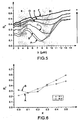
- the Figure 2 demonstrates that the electronic properties of the sub-layer of WO 3-y can be effectively controlled using the flow of oxygen introduced into the enclosure of the frame during the deposition of this layer by magnetron sputtering.
- the material WO 3-y has a resistivity of between 0.5 and 10 -2 ⁇ .cm when the flow of oxygen introduced into the chamber, regulated by optical emission of the tungsten atoms, varies from 9 0 to 9.9 sccm ("standard cubic centimeter per minute") with an argon flow of 70 sccm.
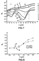
- optical modulation in the infrared is performed in an aqueous liquid medium, namely a slightly acidic electrolyte comprising H 3 PO 4 to 0, 1M, by stacks consisting of a bilayer H x WO 3 / WO 3-y on a glass substrate.
- band II of the infrared range extends between the wavelengths of 3 and 5 microns
- band III of the infrared range extends between the wavelengths of 8 and 12 microns.
- Such a stack which constitutes the "front face” of the device according to the invention can be considered to be representative of the operation of an "all-solid" proton device according to the invention because the layers located under the WO 3-y contribute little or no at all to the optical properties of the device according to the invention.
- the thickness of the WO 3-y material must be less than 500 nm to be permeable to protons.
- the reversible modulation of the optical response in total reflection in the infrared is ensured by the variation of the intercalation rate x, which corresponds to the proton level in the active material H x WO 3 -c.
- X is varied from 0 to 0.5.
- the overall response times for maximum band II contrast are less than 1 minute for a 1 cm 2 area .
Landscapes
- Physics & Mathematics (AREA)
- Nonlinear Science (AREA)
- Chemical & Material Sciences (AREA)
- General Physics & Mathematics (AREA)
- Optics & Photonics (AREA)
- Inorganic Chemistry (AREA)
- Engineering & Computer Science (AREA)
- Crystallography & Structural Chemistry (AREA)
- Electrochemistry (AREA)
- Thermal Sciences (AREA)
- Health & Medical Sciences (AREA)
- Critical Care (AREA)
- Emergency Medicine (AREA)
- General Health & Medical Sciences (AREA)
- Chemical Kinetics & Catalysis (AREA)
- Remote Sensing (AREA)
- Aviation & Aerospace Engineering (AREA)
- Electrochromic Elements, Electrophoresis, Or Variable Reflection Or Absorption Elements (AREA)
Description
- L'invention concerne un dispositif électrochrome tout-solide.
- Plus précisément, l'invention concerne un dispositif électrochrome tout-solide à réflexion ou émission infrarouge contrôlée, notamment de type électrocommandable.
- L'invention a trait, en outre, à un bicouche, aussi appelé électrode bicouche ou composite pour un tel dispositif électrochrome.
- L'invention concerne enfin un procédé de préparation dudit dispositif.
- Le domaine technique de l'invention peut être défini comme celui des dispositifs électrochromes actifs dans l'infrarouge.
- Il existe actuellement deux familles de dispositifs électrochromes actifs dans l'infrarouge, à savoir les dispositifs souples qui peuvent être « tout-organique » exclusivement à base de polymères organiques ou bien hybrides, et les dispositifs « tout-solide » constitués d'empilements de couches inorganiques ou minérales.
- Si l'on s'intéresse aux dispositifs « tout-organique », le document
FR-A1-2 825 481 - Le dispositif décrit dans ce document présente des interfaces fragiles qui limitent sa durée de vie. En effet, l'électrolyte est généralement liquide, et si un défaut d'étanchéité vient à survenir, il peut alors se produire une fuite d'électrolyte conduisant éventuellement à un assèchement du dispositif.
- Le manque d'électrolyte altère gravement les propriétés électrochromes.
- Le document
WO-A1-2010/058108 décrit un dispositif électroémissif comprenant un matériau sous la forme d'un réseau semi-interpénétré de polymères. Ce dispositif présente l'avantage de ne pas nécessiter de couche d'or pour fonctionner. - Bien que présentant une très bonne cyclabilité à température ambiante alliée à une architecture simplifiée, ce dispositif nécessite lui aussi une étape d'imprégnation dans un électrolyte liquide. De plus, les tests réalisés à température élevée révèlent une dégradation des propriétés électrochromes.
- Des dispositifs hybrides sont décrits dans le document
FR-A1-2 879 764 - Le matériau d'insertion WO3.H2O possède une bonne conduction protonique alliée à une réflexion IR modulable sur fond absorbant carboné, perméable aux ions et collecteur de courant.
- Bien que plus robuste que celui du document
FR-A1-2,825,481 - Les dispositifs souples, quels qu'ils soient, présentent en particulier l'inconvénient, notamment lorsqu'ils sont utilisés pour la protection thermique des satellites, d'être peu adaptés aux conditions spatiales.
- En effet, les électrolytes gels posent des problèmes lorsqu'ils sont utilisés sous vide, et les polymères qui constituent les dispositifs souples se déforment sous l'effet de la chaleur et sont peu résistants aux UV.
- Les dispositifs « tout-solide », « commandables », sont le plus souvent conçus pour une application dans le domaine du vitrage, et permettent d'allier confort visuel et confort thermique dans le domaine du visible et du proche Infrarouge (IR).
- Le matériau actif est généralement constitué d'une couche d'oxyde de tungstène poreux et faiblement cristallisé, c'est-à-dire amorphe aux rayons X.
- Cette couche dite couche de HxWO3-a devient absorbante lorsque le matériau est intercalé, en d'autres termes lorsque des protons y sont insérés, à savoir lorsque x>0.
- Un exemple d'un tel dispositif « tout-solide » est décrit dans le document
FR-A1-2 904 704 - Ce dispositif comprend un empilement électrochrome « tout-solide » de structure TC1/EC1/EL/EC2/TC2 avec un substrat porteur muni d'une première couche électroconductrice TC1, une première couche électrochimiquement active EC1 susceptible d'insérer de manière réversible des ions comme des cations tels que H+ ou Li+ ou des anions tels que OH-, notamment en un matériau électrochrome cathodique ou respectivement anodique, une couche d'électrolyte EL, une seconde couche électrochimiquement active EC2 susceptible d'insérer de manière réversible lesdits ions, notamment en un matériau électrochrome cathodique ou respectivement anodique, et une seconde couche électroconductrice TC2.
- Chaque couche électroactive EC1 ou EC2 peut notamment comporter de l'oxyde de tungstène.
- Or, ce dispositif tout-solide ne peut être employé pour une modulation du rayonnement infrarouge moyen, à savoir d'une longueur d'onde généralement de 1,5 à 20 µm, car les électrodes TC1 et TC2 ne sont pas transparentes au-delà de 2 µm, en raison de leur conductivité élevée.
- Ainsi, des problèmes particuliers se posent pour les dispositifs électrochromes « tout-solide », inorganiques, actifs dans l'infrarouge.
- En effet, les dispositifs électrochromes actifs dans l'infrarouge de conception classique nécessitent une électrode transparente dans l'infrarouge afin que la signature du matériau actif puisse être efficace et modulable.
- Ainsi, le document
US-B1-7,265,890 décrit-il un dispositif électrochrome qui comprend sur un substrat rigide ou flexible une électrode constituée par exemple, par un film de métal ou par une couche d'oxyde métallique conducteur tel que l'ITO, une couche électrochrome, par exemple en oxyde de tungstène chargée en ions lithium, une couche de transfert d'ions en nitrure de lithium, une couche d'électrolyte, une couche de stockage d'ions, et une électrode transparente en métal. - Dans ce dispositif, le matériau actif LixWO3 est déposé à l'arrière de l'empilement.
- Les performances d'un tel dispositif sont alors limitées par la transparence aux infrarouges des couches supérieures constituées par l'électrolyte, la contre-électrode réservoir d'ions et l'électrode chargée d'y amener le courant.
- Les empilements actifs dans l'infrarouge, et notamment dans le moyen infrarouge, à savoir d'une longueur d'onde généralement de 1,5 à 20 µm, peuvent comprendre une couche d'oxyde de tungstène HxWO3-a en face avant et absorbante sur fond réflecteur.
- Le document de K. Sauvet, L. Sauques et A. Rougier, Journal of Physics and Chemistry of Solids 71, (2010), 696-699, mentionne l'utilisation d'une grille d'or poreuse réflectrice en tant qu'électrode pour HxWO3-a à l'instar de l'architecture utilisée dans le système souple « tout-organique » du document
FR-A1-2825481 - Toutefois, dans le cas des systèmes complets conçus par ces auteurs, l'emploi d'une électrode transparente aux infrarouges, en plus de la grille d'or à maillage micronique, reste nécessaire afin d'amener les électrons dans le matériau actif.
- Or, les électrodes transparentes dans l'infrarouge sont encore à l'état de recherche, et sont difficilement industrialisables.
- Actuellement, on a recours à des grilles d'or transparentes dans l'infrarouge à maillage submillimétrique réalisées par photolithographie sur verre transparent de type BaF2, ce qui complique de manière drastique la réalisation des dispositifs.
- Ainsi, le document
FR-A1-2934062 - une grille métallique, de préférence en or, transparent dans le domaine infrarouge, formant une première électrode,
- un système fonctionnel électrochrome comprenant une couche d'un premier matériau électrochrome de stockage ionique (EC1), de préférence à base d'oxyde d'iridium, au moins une couche à fonction électrolytique (EL1, EL2) de préférence à base d'oxyde de tantale et d'oxyde de tungstène, et une couche d'un second matériau électrochrome (EC2),
- une couche métallique apte à réfléchir le rayonnement infrarouge, formant une seconde électrode,
- un intercalaire de feuilletage en matériau thermoplastique.
- Il existe donc, au regard de ce qui précède, un besoin pour un dispositif électrochrome, actif dans l'infrarouge, de préférence dans l'infrarouge moyen, notamment à émissivité modulable dans l'infrarouge (IR) qui permette de s'affranchir de l'utilisation d'électrodes transparentes au rayonnement infrarouge et notamment de grilles en or.
- Il existe encore, au regard de ce qui précède, un besoin pour un dispositif électrochrome, actif dans l'infrarouge, de préférence dans l'infrarouge moyen, robuste, possédant une résistance mécanique élevée, résistant aux températures élevées, par exemple supérieures ou égales à 100°C, résistant aux rayonnements ultraviolets, pouvant être placé dans un environnement où règne le vide, par exemple dans l'espace.
- Il existe, également, un besoin pour un dispositif qui puisse être fabriqué par un procédé simple, comportant un nombre limité d'étapes, et d'une durée réduite.
- Le but de la présente invention est de fournir un dispositif électrochrome, actif dans l'infrarouge, de préférence dans l'infrarouge moyen, qui réponde entre autres aux besoins énumérés plus haut.
- Le but de la présente invention est encore de fournir un tel dispositif qui ne présente pas les inconvénients, limitations, défauts et désavantages des dispositifs de l'art antérieur, et qui résolve les problèmes des dispositifs de l'art antérieur.
- Dans la présente description, il est fait référence à un premier matériau électrochrome de stockage protonique. Ce premier matériau électrochrome de stockage protonique de la description correspond au matériau électrochrome de stockage protonique mentionné dans les revendications.
- De même, le second matériau électrochrome à taux d'intercalation protonique variable, choisi parmi l'oxyde de tungstène cristallisé HxWO3-c où x est compris entre 0 et 1, et l'oxyde de tungstène cristallisé hydraté HxWO3.nH20-c où x est compris entre 0 et 1 et n est un nombre entier de 1 à 2, mentionné dans la description, correspond au matériau électrochrome à taux d'intercalation protonique variable, choisi parmi l'oxyde de tungstène cristallisé HxWO3-c où x est compris entre 0 et 1, et l'oxyde de tungstène cristallisé hydraté HxWO3.nH20-c où x est compris entre 0 et 1 et n est un nombre entier de 1 à 2, mentionné dans les revendications.
- Ce but, et d'autres encore sont atteints, conformément à la présente invention, par un dispositif électrochrome tout-solide à réflexion ou émission infrarouge contrôlée, notamment de type électrocommandable, comprenant un empilement, ledit empilement comprenant successivement depuis une face arrière jusqu'à une face avant exposée aux rayons infrarouges :
- a) un substrat en un matériau conducteur électronique, ou un substrat en un matériau non conducteur électronique recouvert d'une couche en un matériau conducteur électronique, ledit substrat en un matériau conducteur électronique ou ladite couche en un matériau conducteur électronique formant une première électrode ;
- b) une couche en un premier matériau électrochrome de stockage protonique ;
- c) une couche d'un électrolyte conducteur protonique et isolant électronique ;
- d) un bicouche comprenant une couche d'un oxyde de tungstène sous stoechiométrique, non électrochrome, WO3-y où y est compris entre 0,2 et 1, optiquement absorbante dans l'infrarouge (de préférence dans le moyen infrarouge), conductrice électronique, poreuse, formant une seconde électrode ; ladite couche d'oxyde de tungstène WO3-y étant disposée sous une couche à réflexion variable dans l'infrarouge, d'un second matériau électrochrome à taux d'intercalation protonique variable, choisi parmi l'oxyde de tungstène cristallisé HxWO3-c où x est compris entre 0 et 1, et l'oxyde de tungstène cristallisé hydraté HxWO3.nH2O-c où x est compris entre 0 et 1 et n est un nombre entier de 1 à 2.
- e) une couche de protection, transparente aux rayons infrarouges, en un matériau inorganique.
- La couche à réflexion variable qui fait partie du bicouche d) est plus ou moins réfléchissante ou même pas du tout réfléchissante selon la valeur de x.
- Ainsi pour x = 0, cette couche n'est pas réfléchissante et pour les valeurs de x au-delà de 0,1, cette couche est réfléchissante.
- Avantageusement, ledit substrat lorsqu'il est en un matériau conducteur électronique, peut être en un matériau choisi parmi les matériaux résistants mécaniquement et chimiquement aux sollicitations du milieu extérieur (par exemple dans l'espace) et chimiquement compatible vis-à-vis d'un fonctionnement protonique et notamment chimiquement compatible vis-à-vis du premier matériau électrochrome de stockage protonique, de préférence ledit matériau conducteur électronique est choisi parmi les métaux tels que l'aluminium, le platine ou le chrome, et leurs alliages.
- Par matériau « chimiquement compatible vis-à-vis d'un fonctionnement protonique », on entend généralement un matériau dont les propriétés (chimiques, physiques, mécaniques, électroniques) ne sont pas dégradées lors d'un fonctionnement du dispositif avec des protons.
- Par « chimiquement compatible vis-à-vis du premier matériau électrochrome de stockage protonique », on entend généralement que le matériau conducteur électronique réagit peu ou pas avec le premier matériau électrochrome de stockage protonique, ou encore que le matériau conducteur électronique est inerte vis-à-vis du premier matériau électrochrome de stockage protonique.
- De manière générale, dans la présente, on entend généralement qu'un premier matériau est chimiquement compatible avec un deuxième matériau, lorsque ce premier matériau réagit peu ou pas avec le deuxième matériau, ou encore que le premier matériau est inerte vis-à-vis du deuxième matériau.
- Avantageusement, ledit substrat lorsqu'il est en un matériau non conducteur électronique peut être en un matériau choisi parmi les matériaux résistants mécaniquement et chimiquement aux sollicitations du milieu extérieur (par exemple dans l'espace) et chimiquement compatibles vis-à-vis d'un fonctionnement protonique et notamment chimiquement compatibles vis-à-vis du premier matériau électrochrome de stockage protonique, de préférence ledit matériau non conducteur électronique est choisi parmi les verres et les polymères organiques résistants mécaniquement et chimiquement, tels que le Poly (Téréphtalate d'éthylène) ou PET.
- Avantageusement, la couche en un matériau conducteur électronique peut être en un matériau choisi parmi les matériaux résistants mécaniquement et chimiquement aux sollicitations du milieu extérieur (par exemple dans l'espace), et chimiquement compatibles vis-à-vis d'un fonctionnement protonique et notamment chimiquement compatibles vis-à-vis du premier matériau électrochrome de stockage protonique, de préférence ledit matériau conducteur électronique est choisi parmi les métaux tels que l'aluminium, le platine, le chrome et leurs alliages ; et les oxydes métalliques conducteurs électroniques tels que l'oxyde d'indium dopé à l'étain ou ITO et l'oxyde d'étain dopé au fluor ou FTO.
- Avantageusement, le premier matériau électrochrome de stockage protonique peut être choisi parmi les matériaux électrochromes de stockage protonique chimiquement compatibles vis-à-vis d'un fonctionnement protonique, notamment chimiquement compatibles vis-à-vis de l'électrolyte conducteur protonique et isolant électronique, de préférence le premier matériau électrochrome de stockage protonique peut être choisi parmi les oxydes métalliques hydratés de préférence amorphes tels que l'oxyde de tungstène hydraté HxWO3.nH2O, ou x est compris entre 0 et 1, et n est un nombre entier de 1 à 2, et les mélanges de deux ou plus desdits oxydes.
- Avantageusement, l'électrolyte conducteur protonique et isolant électronique peut être choisi parmi les électrolytes conducteurs protoniques et isolants électroniques chimiquement compatible vis-à-vis d'un fonctionnement protonique, notamment chimiquement compatibles (inertes) vis-à-vis de l'oxyde de tungstène cristallisé HxWO3-c (oxyde de tungstène protoné) ou de l'oxyde de tungstène cristallisé hydraté HxWO3.nH2O-c, de préférence l'électrolyte conducteur protonique et isolant électronique peut être choisi parmi les oxydes métalliques hydratés, de préférence amorphes tels que l'oxyde de tantale Ta2O5 hydraté amorphe, l'oxyde de zirconium hydraté amorphe et les mélanges de deux ou plus desdits oxydes.
- L'électrolyte est hydraté et amorphe afin qu'il puisse facilement transporter les protons du matériau de stockage vers le matériau actif en réflexion infrarouge. L'oxyde métallique de l'électrolyte doit généralement être différent de l'oxyde de tungstène.
- Avantageusement, la couche de protection transparente aux rayons infrarouges, peut être en un matériau choisi parmi les matériaux compatibles vis-à-vis d'un fonctionnement protonique, notamment chimiquement compatibles vis-à-vis de l'oxyde de tungstène cristallisé HxWO3-c ou de l'oxyde de tungstène cristallisé hydraté HxWO3.nH2O-c, de préférence la couche de protection transparente aux rayons infrarouges peut être en un matériau choisi parmi les matériaux inorganiques non toxiques, de préférence parmi les oxydes de métaux et de métalloïdes, de préférence, denses, tels que l'oxyde de cérium CeO2, l'oxyde d'yttrium Y2O3, la silice SiO2 et les mélanges de deux ou plus desdits oxydes de métaux ou de métalloïdes.
- Par oxydes de métaux ou de métalloïdes denses, on entend généralement que ces oxydes ont une densité supérieure à 99% de la densité théorique.
- Avantageusement, le substrat (conducteur électronique ou non) a une épaisseur de 0,175 mm à 1 mm.
- Avantageusement, la couche en un matériau conducteur électronique qui recouvre le substrat lorsque celui-ci est un substrat en un matériau non conducteur électronique, a une épaisseur de 50 à 150 nm.
- Avantageusement, la couche en un premier matériau électrochrome de stockage protonique a une épaisseur de 0,2 à 1 µm, de préférence de 0,4 à 1 µm.
- Avantageusement, la couche en un électrolyte conducteur protonique et isolant électronique a une épaisseur de 0,2 à 1 µm, de préférence de 0,4 à 1 µm.
- Avantageusement, la couche en oxyde de tungstène WO3-y a une épaisseur 0,2 à 0,5 µm, de préférence de 0,4 à 0,5 µm.
- Avantageusement, la couche d'un second matériau électrochrome a une épaisseur 0,2 à 1 µm, de préférence de 0,3 à 0,8 µm.
- Avantageusement, la couche de protection transparente aux rayons infrarouges a une épaisseur de 0,1 à 1 µm, de préférence de 0,4 à 1 µm.
- Le dispositif selon l'invention comprend un empilement spécifique de couches spécifiques dans un ordre spécifique qui n'a jamais été décrit dans l'art antérieur tel que représenté notamment par les documents relatifs à des dispositifs électrochromes « tout-solide » mentionnés plus haut.
- Le dispositif selon l'invention peut être défini comme un dispositif tout-solide électrochrome à réflexion ou émissivité modulable dans l'infrarouge (IR) en particulier dans l'infrarouge moyen (longueurs d'onde de 1,5 à 20 µm) et notamment dans la bande II (longueur d'onde de 3 à 5 µm) et/ou dans la bande III (longueur d'onde de 8 à 12 µm) du spectre infrarouge, dont la partie active est un bicouche, que l'on pourrait aussi appeler électrode composite ou bicouche, à base d'oxyde de tungstène qui est selon l'invention située en face avant du dispositif.
- La gamme de longueurs d'ondes d'intérêt préférée pour le dispositif selon l'invention se situe en effet dans le moyen infrarouge (« MIR ») c'est-à-dire dans une gamme de longueurs d'onde de 1,5 à 20 µm, notamment de 2 à 20 µm, qui est une gamme privilégiée pour les applications spatiales alors que pour des applications de type vitrage, les gammes de longueur d'onde d'intérêt se situent dans le Visible - Proche Infrarouge.
- Le fait de disposer la partie active du dispositif électrochrome et notamment la couche du second matériau électrochrome à taux d'intercalation protonique variable, en face avant du dispositif, c'est-à-dire du côté du dispositif qui est directement exposé aux rayons infrarouges n'a jamais été décrit jusqu'alors dans les dispositifs « tout-solide » et est à l'origine de nombre des avantages du dispositif selon l'invention.
- En effet, ce bicouche, cette électrode composite, exposé directement au rayonnement IR, est capable, par insertion électrochimique réversible de protons (qui ont été préférés aux ions lithium pour des raisons cinétiques), de moduler l'émissivité infrarouge totale du système comme cela est largement démontré dans les exemples fournis plus loin, et cela indépendamment des autres constituants sous-jacents de l'empilement.
- La couche active du second matériau électrochrome à taux d'intercalation protonique variable, constitue la première couche de la face avant du dispositif. Aucun obstacle, tel qu'une électrode, ne fait donc obstacle à son exposition aux rayons infrarouges, et aucune perte optique n'est créée, car la couche d'oxyde de tungstène formant la seconde électrode est disposée sur la face de la couche active du second matériau électrochrome opposée à la face exposée aux rayonnements infrarouges.
- Dans le dispositif selon l'invention, on surmonte l'un des inconvénients majeurs des dispositifs « tout-solide » de l'art antérieur dans lesquels la couche active est disposée sous une électrode, qui doit être obligatoirement transparente aux rayonnements infrarouges avec toutes les difficultés de réalisation que cela implique.
- En particulier, le dispositif selon l'invention ne comporte pas de grille d'or, ce qui simplifie grandement la fabrication du dispositif selon l'invention et en abaisse grandement le coût.
- Plus précisément, on fournit selon l'invention, pour la première fois, un dispositif tout-solide, non organique, qui ne comporte pas d'électrode transparente aux rayonnements infrarouges telle qu'une grille d'or.
- En d'autres termes, les performances optiques du dispositif selon l'invention sont produites par les propriétés électroniques intrinsèques du matériau actif électrochrome situé en face avant de l'empilement.
- On peut ainsi bénéficier de la réponse optique optimale du système, indépendamment des couches situées derrière la face avant.
- On peut dire que le dispositif selon l'invention est réalisé selon une conception optimisée qui n'a jamais été décrite ni suggérée dans l'art antérieur relatif aux dispositifs « tout-solide ».
- Le dispositif selon l'invention est, en outre, caractérisé en ce qu'il comprend un bicouche, que l'on pourrait aussi appeler électrode composite ou bicouche, constitué d'une couche d'oxyde de tungstène active, électrochrome, réflectrice, cristallisée et/ou hydratée de formule HxWO3-c ou WO3.nH2O-c à taux d'intercalation protonique (défini par x) variable en fonction de la tension appliquée (bornes comprises généralement entre +3 et -3 Volts).
- Cette couche active, électrochrome est selon l'invention elle-même déposée sur une couche d'oxyde de tungstène sous-stoechiométrique absorbante de formule WO3-y.
- Le bicouche produit à lui-seul un contraste optique variable dans l'infrarouge, de préférence dans le moyen infrarouge (2 à 50 µm).
- Dans le dispositif selon l'invention, l'effet technique produit par la nature différente des deux couches qui constituent le bicouche n'est pas d'accroître l'absorption du dispositif qui est fixée par la couche de WO3-y, mais au contraire de la diminuer par augmentation de la réflexion de la couche d'un second matériau électrochrome HxWO3-c ou WO3.nH2O-c. Ce second matériau électrochrome est nécessairement à l'état cristallisé afin qu'une augmentation du taux d'intercalation d'ions x (ici il s'agit généralement de protons H+) produise dans la couche de ce second matériau électrochrome une augmentation de la réflexion infrarouge R.
- En d'autres termes, la couche du second matériau électrochrome HxWO3-c ou WO3.nH2O-c devient réflectrice lorsqu'elle est intercalée, accroissant ainsi la modulation d'émissivité du dispositif.
- Dans ce bicouche ou électrode composite, la sous-couche de WO3-y qui est une électrode poreuse, joue un triple rôle :
- elle assure un fond absorbant optique au système ;
- elle permet la diffusion des protons ;
- elle assure un apport électronique dans le matériau actif HxWO3-c.
- On peut dire que la sous-couche de WO3-y du bicouche ou électrode composite possède une fonction « 3 en 1 », ce qui permet par exemple d'utiliser une seule cible de tungstène pour réaliser un empilement simplifié. Un autre matériau par exemple sous la forme d'une grille d'or n'est, en effet, pas nécessaire pour amener les électrons dans le matériau actif HxWO3-c ou WO3.nH2O-c.
- La sous-couche de WO3-y est dans un état sous-stoechiométrique, elle est nécessairement non-électrochrome, et elle sert de référence optique absorbante infrarouge par rapport à une couche supérieure active dans l'infrarouge. La sous-couche de WO3-y est de préférence absorbante dans le moyen infrarouge.
- Le dispositif « tout-solide » selon l'invention est compatible avec toutes les exigences qui régissent une utilisation dans l'espace, en effet les matériaux entièrement inorganiques qui le constituent lui permettent de résister aux agressions UV, au vide et aux températures élevées, par exemple voisines de 100°C, au contraire des dispositifs souples existants dont les électrolytes gels supportent mal une mise sous vide et dont les polymères se déforment sous l'effet de la chaleur et sont peu résistants au UV.
- Le dispositif selon l'invention peut être qualifié, de dispositif électrochrome robuste, durable, de conception simplifiée.
- Le dispositif selon l'invention présente, en outre, l'avantage de pouvoir être réalisé très simplement, en un nombre limité d'étapes, par un seul et même procédé de dépôt pour toutes les couches.
- Le dispositif selon l'invention peut donc être réalisé en une durée réduite et avec des coûts réduits.
- Ainsi, le dispositif selon l'invention peut être entièrement réalisé sous vide à l'aide d'une même technologie de dépôt physique en phase vapeur (« PVD » ou « Physical Vapour Deposition » en anglais) choisi par exemple parmi la pulvérisation cathodique, l'ablation laser, ou l'évaporation.
- L'invention concerne, en outre, un bicouche pour un dispositif électrochrome comprenant une couche d'un oxyde de tungstène sous stoechiométrique, non électrochrome, WO3-y où y est compris entre 0,2 et 1, optiquement absorbante dans l'infrarouge (de préférence dans le moyen infrarouge), conductrice électronique, poreuse, formant une électrode ; ladite couche d'oxyde de tungstène WO3-y étant disposée sous une couche à réflexion variable dans l'infrarouge, d'un second matériau électrochrome à taux d'intercalation protonique variable, choisi parmi l'oxyde de tungstène cristallisé HxWO3-c où x est compris entre 0 et 1, et l'oxyde de tungstène cristallisé hydraté HxWO3.nH2O-c où x est compris entre 0 et 1 et n est un nombre entier de 1 à 2.
- Les avantages liés à la structure et à la composition spécifique de ce bicouche ont pour la plupart déjà été exposés plus haut dans le cadre de la description du dispositif.
- L'invention concerne aussi un procédé de préparation du dispositif selon l'invention, tel que décrit plus haut, dans lequel on réalise les étapes successives suivantes :
- a) on dépose une couche en un premier matériau électrochrome de stockage protonique sur un substrat en un matériau conducteur électronique, ou sur une couche en un matériau conducteur électronique disposée sur un substrat en un matériau non conducteur électronique ledit substrat en un matériau conducteur électronique ou ladite couche en un matériau conducteur électronique formant une première électrode ;
- b) on dépose une couche d'un électrolyte conducteur protonique et isolant électronique sur la couche en un premier matériau électrochrome de stockage protonique ;
- c) on dépose une couche d'un oxyde de tungstène sous stoechiométrique, non-électrochrome, WO3-y où y est compris entre 0,2 et 1, optiquement absorbante dans l'infrarouge, conductrice électronique, poreuse, formant une seconde électrode, sur la couche d'un électrolyte conducteur protonique et isolant électronique ;
- d) on dépose une couche à réflexion variable dans l'infrarouge d'un second matériau électrochrome à taux d'intercalation protonique variable, choisi parmi l'oxyde de tungstène cristallisé HxWO3-c où x est compris entre 0 et 1 et l'oxyde de tungstène cristallisé hydraté HxWO3.nH2O-c où x est compris entre 0 et 1 et n est un nombre entier de 1 à 2, sur la couche d'un oxyde de tungstène sous stoechiométrique, non-électrochrome, WO3-y;
- e) on dépose une couche de protection, transparente aux rayons infrarouges, en un matériau inorganique, sur la couche à réflexion variable dans l'infrarouge d'un second matériau électrochrome.
- Le procédé selon l'invention est fiable et beaucoup plus simple que les procédés de l'art antérieur.
- Avantageusement, les couches sont déposées par un procédé de dépôt Physique en phase vapeur ou PVD choisi parmi la pulvérisation cathodique, l'ablation laser et l'évaporation.
- Avantageusement, toutes les couches sont déposées sous vide par un même procédé de dépôt physique en phase vapeur, de préférence par pulvérisation cathodique magnétron réactive.
- Pour des raisons technico-économiques, la pulvérisation cathodique magnétron en mode réactif sera privilégiée car elle assure notamment un bon contrôle du taux d'oxygène dans le plasma, des vitesses de dépôt élevées, par exemple d'environ 60 nm/min, une bonne qualité optique du matériau actif.
- En outre, elle permet de préparer le matériau cristallisé HxWO3-c ou HxWO3.nH2O-c en face avant sans échauffer le reste de l'empilement.
- Avantageusement, toutes les étapes sont réalisées dans une même enceinte sous vide, sans ouverture de l'enceinte entre chacune des étapes, ce qui occasionne une simplification importante du procédé, un gain de temps important sans perte de protons, et des coûts réduits.
- L'invention concerne, en outre, l'utilisation du dispositif tel que décrit plus haut pour la protection thermique d'un objet.
- Cet objet peut être notamment un véhicule et notamment un véhicule spatial tel qu'un satellite.
- L'utilisation du dispositif selon l'invention est particulièrement avantageuse dans le cas de véhicules tels que les satellites soumis à des contraintes, limitations sur leur masse embarquée. En effet, le dispositif selon l'invention est d'une faible masse et permet un gain de masse important par rapport aux dispositifs, par exemple les dispositifs mécaniques, couramment mis en oeuvre pour la protection thermique, notamment dans les satellites.
- D'autres avantages de l'invention apparaîtront mieux à la lecture de la description détaillée qui va suivre faite en relation avec les dessins joints.
-
- La
Figure 1 est une vue schématique du dispositif selon l'invention. - La
Figure 2 est un graphique qui représente la résistivité (en 10-2 Ohm.cm) de la sous couche WO3-y en fonction du débit d'oxygène (en sccm) introduit dans l'enceinte du bâti de l'appareil de pulvérisation cathodique magnétron lors du dépôt de cette couche par cette technique. - La
Figure 3 est un graphique qui illustre le pilotage électrochimique du matériau actif HxWO3-c, entre 0,2 V (x = 0) et -0,8 V (x = 0,5), par rapport à une électrode de référence de type ECS en milieu H3PO4 - 0,1 M.
En ordonnée est porté le coefficient de réflexion totale RT dans le domaine de l'infrarouge de la partie active de l'empilement HxWO3-c (320 nm) / WO3-y (400 nm) / verre et, en abscisse est portée la longueur d'onde λ (en µm) du rayonnement infrarouge.
Les courbes A, B, C, D, E, F, G correspondent respectivement à des valeurs de x de 0 ; 0,05 ; 0,1 ; 0,2 ; 0,25 ; 0,35 ; et 0,5. - La
Figure 4 est un graphique qui donne la moyenne du coefficient de réflexion totale RT produite par la partie active de l'empilement HxWO3-c (320 nm) / WO3-y (400 nm) / verre dans les bandes II (courbe A) et III (courbe B), en fonction du taux d'intercalation x dans HxWO3-c. - La
Figure 5 est un graphique qui illustre le pilotage électrochimique du matériau actif HxWO3-c, entre 0,2 V (x = 0) et -0,8 V (x = 0,5), par rapport à une électrode de référence de type ECS en milieu H3PO4-0,1 M.
En ordonnée est porté le coefficient de réflexion totale RT dans le domaine de l'infrarouge de la partie active de l'empilement HxWO3-c (560 nm) / WO3-y (400 nm) / verre et, en abscisse est portée la longueur d'onde λ (en µm) du rayonnement infrarouge.
Les courbes A, B, C, D, E, F correspondent respectivement à des valeurs de x de 0 ; 0,1 ; 0,2 ; 0,3 ; 0,4 ; et 0,5. - La
Figure 6 est un graphique qui donne la moyenne du coefficient de réflexion totale RT produite par la partie active de l'empilement HxWO3-c (560 nm) / WO3-y (400 nm) / verre dans les bandes II (courbe A) et III (courbe B), en fonction du taux d'intercalation x dans HxWO3-c. - La
Figure 7 est un graphique qui illustre le pilotage électrochimique du matériau actif HxWO3-c, entre 0,2 V (x = 0) et -0,8 V (x = 0,5), par rapport à une électrode de référence de type ECS en milieu H3PO4-0,1M.
En ordonnée est porté le coefficient de réflexion totale RT dans le domaine de l'infrarouge de la partie active de l'empilement HxWO3-c (730 nm) / WO3-y (400 nm) / verre et en abscisse est portée la longueur d'onde λ (en µm) du rayonnement infrarouge.
Les courbes A, B, C, D, E, F correspondent respectivement à des valeurs de x de 0 ; 0,1 ; 0,2 ; 0,3 ; 0,4 ; et 0,5. - La
Figure 8 est un graphique qui donne la moyenne du coefficient de réflexion totale RT produite par la partie active de l'empilement HxWO3-c (730 nm) / WO3-y (400 nm) / verre dans les bandes II (courbe A) et III (courbe B), en fonction du taux d'intercalation x dans HxWO3-c. - La
Figure 1 représente un dispositif selon l'invention comprenant le bicouche spécifique selon l'invention. - Ce dispositif comporte une face avant (1) exposée au rayonnement infrarouge (2) et une face arrière (3) qui n'est pas exposée directement aux rayons infrarouges.
- Le dispositif selon l'invention comprend tout d'abord un substrat ou support (4), qui joue essentiellement un rôle de support métallique du dispositif.
- Le substrat ou support (4) ne présente généralement pas de transparence aux rayons infrarouges.
- Le substrat ou support est généralement en un matériau léger.
- Ce substrat ou support (4) peut être en un matériau choisi parmi les métaux, les verres tels que le verre de lame de microscope, et les polymères organiques qui présentent une rigidité suffisante, tels que le Poly (téréphtalate d'éthylène) ou PET.
- Les métaux qui peuvent constituer le substrat ou support (4), peuvent être choisis par exemple, parmi l'aluminium, le platine, le chrome, et leurs alliages.
- Dans le cas où le substrat ou support (4) est en un matériau qui n'est pas conducteur électronique tel que le verre ou le PET, alors une couche en un matériau conducteur électronique est déposée sur le substrat ou plus exactement sur la surface supérieure de celui-ci.
- Cette couche en un matériau conducteur électronique joue le rôle d'électrode reliée à l'alimentation du dispositif.
- Ce matériau conducteur électronique est généralement choisi parmi les métaux, et les oxydes métalliques conducteurs électroniques.
- Les métaux qui peuvent constituer la couche en un matériau conducteur électronique peuvent être choisis parmi les métaux déjà cités plus haut qui peuvent constituer le substrat ou support.
- Les oxydes métalliques conducteurs électroniques sont bien connus de l'homme du métier.
- Des exemples de tels oxydes conducteurs sont l'oxyde d'indium dopé à l'étain (« Indium Tin Oxide » ou ITO en anglais), l'oxyde d'étain SnO2 dopé ou fluor (« Fluor Tin Oxide » ou FTO en anglais).
- Le matériau conducteur électronique de ladite couche, notamment lorsqu'il s'agit d'un oxyde métallique conducteur électronique est généralement choisi parmi les matériaux qui peuvent être déposés en couche mince par un procédé PVD, tel que la pulvérisation cathodique, l'ablation laser ou l'évaporation, et de préférence parmi les matériaux qui peuvent être déposés en couche mince par pulvérisation cathodique.
- Dans le cas où le substrat ou support est en un matériau qui est conducteur électronique tel qu'un métal, alors il n'est pas nécessaire qu'une couche en un matériau conducteur électronique soit déposée sur le substrat.
- Le support ou substrat (4), que l'on peut alors qualifier de substrat « monobloc », joue dans ce cas à la fois le rôle de support mécanique du dispositif déjà indiqué plus haut et le rôle d'électrode reliée à l'alimentation du dispositif.
- Sur la
Figure 1 , c'est ce mode de réalisation, sans couche en un matériau conducteur électronique sur le substrat, qui est représenté. - Il est important que le matériau qui constitue la couche en un matériau conducteur électronique lorsque celle-ci est présente, ou le matériau conducteur électronique qui constitue le substrat lorsque ladite couche n'est pas présente, soit chimiquement compatible avec le matériau de la couche d'un premier matériau électrochrome de stockage protonique (5) déposée sur le substrat ou sur la couche en un matériau conducteur électronique.
- On choisira donc le matériau qui constitue la couche en un matériau conducteur électronique, ou le matériau conducteur électronique qui constitue le substrat de manière à ce qu'il soit chimiquement compatible avec un milieu protoné, tel qu'un oxyde métallique hydraté.
- Le substrat (4) a généralement une épaisseur de 0,175 à 1 mm.
- Le substrat (4) se présente généralement sous la forme d'une feuille de matériau léger.
- Ainsi, l'épaisseur du substrat (4) est généralement d'environ 1 mm dans le cas d'un substrat en verre et d'environ 175 µm dans le cas d'un substrat en polymère, par exemple d'un substrat en PET.
- La couche en un matériau conducteur électronique éventuelle a généralement une épaisseur de 50 à 150 nm.
- Sur le substrat ou la couche en un matériau conducteur électronique est disposée une couche en un premier matériau électrochrome de stockage protonique (5). Cette couche peut aussi être dénommée contre-électrode réservoir de protons.
- Le premier matériau électrochrome de stockage protonique peut être choisi parmi tous les oxydes métalliques hydratés électrochromes, et les mélanges de deux ou plus de ces oxydes.
- Des exemples de tels oxydes sont l'oxyde de tungstène hydraté HxWO3.nH2O, où x est compris entre 0 et 1 (0 et 1 inclus), et n est un nombre entier de 1 à 2, par exemple n = 1.
- Le choix de ce dernier oxyde analogue à celui du bicouche, présente l'avantage de simplifier encore le procédé de préparation du dispositif selon l'invention en réduisant le nombre de cibles, précurseurs mis en oeuvre.
- Le premier matériau électrochrome de stockage protonique est généralement choisi parmi les matériaux qui peuvent être déposés en couche mince par un procédé PVD tel que la pulvérisation cathodique, l'ablation laser ou l'évaporation, et de préférence parmi les matériaux qui peuvent être déposés en couche mince par pulvérisation cathodique.
- On choisira le premier matériau électrochrome de stockage protonique de manière à ce qu'il soit chimiquement compatible avec l'électrolyte conducteur protonique déposé sur la couche de premier matériau électrochrome.
- La couche en un premier matériau électrochrome de stockage protonique (5) a généralement une épaisseur de 0,2 à 1 µm, de préférence de 0,4 à 1 µm.
- Sur la couche en un premier matériau électrochrome de stockage protonique (5) est disposée une couche en un électrolyte conducteur protonique et isolant électronique (6).
- Cet électrolyte conducteur protonique peut être choisi parmi tous les oxydes métalliques hydratés, de préférence amorphes, et les mélanges de deux ou plus de ces oxydes.
- En effet, les oxydes amorphes conduisent bien mieux les protons.
- Des exemples de tels oxydes sont l'oxyde de tantale Ta2O5 hydraté amorphe et l'oxyde de zirconium hydraté amorphe.
- La couche en un électrolyte conducteur protonique et isolant électronique (6) a généralement une épaisseur de 0,2 à 1 µm, de préférence de 0,4 à 1 µm.
- Sur la couche en un électrolyte conducteur protonique (6) est disposée le bicouche que l'on peut aussi appeler électrode bicouche ou électrode composite (7) selon l'invention.
- Tout d'abord, sur la couche en un électrolyte conducteur protonique est disposée une couche d'un oxyde de tungstène WO3-y où y est compris entre 0,2 et 1 sous stoechiométrique, non électrochrome, optiquement absorbante dans l'infrarouge (8), formant une seconde électrode conductrice électronique reliée à l'alimentation du dispositif.
- Cette couche d'oxyde de tungstène est chimiquement compatible avec les matériaux qui l'entourent, à savoir avec l'électrolyte conducteur protonique de la couche sous-jacente (6) et avec l'oxyde de tungstène cristallisé éventuellement hydraté HxWO3-c ou HxWO3.nH2O-c de la couche immédiatement supérieure (9) de l'empilement de couches du dispositif.
- Cette couche d'un oxyde de tungstène WO3-y (8), est une couche poreuse, avec une taille de pores submicronique, par exemple de 10 à 100 nm.
- Le rôle de cette couche d'oxyde de tungstène WO3-y (8) est triple.
- Ce rôle est en effet d'assurer un fond absorbant optique au système, tout en permettant la diffusion des protons et un apport électronique dans le matériau actif HxWO3-c ou HxWO3.nH2O-c.
- La couche en oxyde de tungstène WO3-y (8) a généralement une épaisseur de 0,2 à 0,5 µm, de préférence de 0,4 à 0,5 µm.
- En effet, l'épaisseur de la couche d'oxyde de tungstène WO3-y (8) doit généralement être inférieure ou égale à 500 nm pour être perméable aux protons. En revanche, cette épaisseur doit généralement être supérieure à 200 nm pour constituer un fond absorbant, ce qui permet de découpler la fonction optique de la face avant du dispositif constituée essentiellement par le bicouche (7), de la fonction électrochimique conférée par le reste de l'empilement, sous la couche d' oxyde de tungstène WO3-y (8) .
- Sur la couche d'oxyde de tungstène WO3-y, (8) est disposée une couche (9) en un second matériau électrochrome choisi parmi l'oxyde de tungstène cristallisé HxWO3-c où x est compris entre 0 et 1 et l'oxyde de tungstène cristallisé hydraté HxWO3.nH2O-c où x est compris entre 0 et 1 et n est compris entre 1 et 2.
- Cette couche en un second matériau électrochrome (9) est généralement une couche poreuse avec une porosité submicronique, par exemple de 10 à 100 nm.
- Cette couche en un second matériau électrochrome (9) est une couche à réflexion variable vis-à-vis des rayons IR.
- Dans cette couche, le matériau actif est un oxyde de tungstène cristallisé représenté par la formule HxWO3-c, qui peut être hydraté afin d'en améliorer les performances, et essentiellement la conductivité protonique.
- Cet oxyde de tungstène cristallisé hydraté est représenté par la formule HxWO3.nH2O-c.
- Dans ces formules, x qui représente le taux d'intercalation du matériau actif HxWO3-c ou HxWO3.nH2O-c est variable et est généralement compris entre 0 et 1 (0 et 1 inclus), tandis que n est généralement compris entre 1 et 2 (1 et 2 inclus).
- La réponse optique du dispositif suit très finement les variations de x, avec une modulation possible à 0,05 près, du fait de la capacité des couches inorganiques à conserver leur taux de protons, encore appelée « effet mémoire ».
- En d'autres termes, les propriétés optiques, la réponse optique, de la couche d'oxyde de tungstène active, électrochrome, réflectrice, cristallisée et/ou hydratée de formule HxWO3-c ou WO3.nH2O-c (9) peuvent être facilement modulées en fonction du taux d'intercalation protonique (défini par x) qui est lui-même variable en fonction de la tension appliquée.
- Ainsi en modifiant cette tension, on pourra agir à volonté sur les propriétés optiques du dispositif. Par exemple, pour une tension appliquée de 0,2 V, x = 0, et pour une tension appliquée de - 0,8 V, x = 0,5.
- Il est à noter que l'oxyde de tungstène WO3, qui constitue la partie active de l'empilement du dispositif selon l'invention est un matériau capable de fonctionner avec des ions lithium et/ou avec des protons.
- Selon l'invention, on choisit de faire fonctionner l'oxyde de tungstène WO3 avec des protons plutôt qu'avec des ions Li+, pour des raisons liées à la cinétique.
- En effet, les dispositifs « tout-solide » tels que le dispositif selon l'invention étant plus lents que les dispositifs souples, il est préférable de travailler avec un second matériau électrochrome protonique, avec un électrolyte inorganique au proton par exemple de type oxyde de tantale Ta2O3 hydraté, et enfin avec une contre-électrode inorganique également au proton.
- La couche en second matériau actif électrochrome (9) a généralement une épaisseur de 0,2 à 1 µm, de préférence de 0,3 à 0,8 µm.
- Les propriétés optiques du dispositif sont adaptables dans le moyen infrarouge avec l'épaisseur de matériau actif HxWO3-c, ou HxWO3.nH2O-c notamment sur les bandes II 3-5 µm) et III (8-12 um) de transparence de l'atmosphère.
- Par exemple, une faible épaisseur (par exemple environ 300 nm) de matériau actif (9) donnera une modulation privilégiée de la réflexion totale dans la bande II tandis qu'une épaisseur élevée (par exemple environ 700 à 800 nm) de matériau actif donnera une modulation privilégiée de la réflexion totale dans la bande III.
- En résumé, les propriétés optiques, le contraste optique, du dispositif selon l'invention peuvent être modulés dans l'infrarouge et notamment dans l'infrarouge moyen en faisant varier x et l'épaisseur du matériau actif HxWO3-c ou HxWO3.nH2O-c.
- Sur la couche en second matériau actif électrochrome (9) est disposée une couche (10) de protection de l'empilement, transparente aux rayons infrarouges, et de préférence réfléchissante vis-à-vis du rayonnement solaire.
- Cette couche (10) peut aussi être appelée couche d'encapsulation.
- En effet, cette couche (10) est déposée lors d'une étape finale sur l'ensemble de l'empilement décrit plus haut afin de conserver la teneur en ions (protons) à l'intérieur du dispositif, et de servir ainsi de matériau d'encapsulation.
- Par transparente aux rayons infrarouges, on entend généralement que cette couche (10) est transparente aux rayons infrarouges de longueurs d'ondes comprises entre 1,5 µm et 20 pm, de préférence entre 3 µm et 12 µm.
- Par faible indice de réfraction, on entend généralement que cette couche (10) a un indice de réfraction entre 1 et 2.
- Cette couche (10) est généralement en un matériau inorganique non toxique.
- De préférence, cette couche (10) est en un matériau choisi parmi les oxydes de métaux et de métalloïdes, et les mélanges de deux ou plus de ces oxydes de métaux et oxydes de métalloïdes.
- Ce ou ces oxyde(s) de métaux ou de métalloïdes, de préférence amorphes, sont choisis de préférence parmi les oxydes qui peuvent être facilement déposés par PVD à partir d'une cible d'oxyde ou de métal, tel que l'oxyde de cérium CeO2, l'oxyde d'yttrium Y2O3, ou SiO2.
- La couche (10) de protection de l'empilement a généralement une épaisseur 0,1 à 1 µm, de préférence de 0,4 à 1 µm.
- Le dispositif selon l'invention comprend, en outre, des moyens (11, 12) pour établir une tension variable entre les électrodes, par exemple une tension variable entre +3 Volts et -3 Volts.
- Le dispositif selon l'invention est préparé par le procédé décrit plus haut.
- L'appareil utilisé pour mettre en oeuvre le procédé selon l'invention pour préparer le dispositif selon l'invention peut être par exemple un bâti de dépôt sous vide (Physical Vapour Deposition ou « PVD » en anglais) comprenant :
- une enceinte sous vide, d'un volume par exemple de 0,1 m3 dans laquelle règne une pression initiale par exemple d'environ 5 10-7 mbar, la vitesse de pompage maximale pour réaliser le vide dans l'enceinte étant de 900 L/s avec une enceinte initialement remplie d'azote ;
- au plus 6 cathodes d'un diamètre de 3 pouces (ou 76 mm), ou bien 2 cathodes d'un diamètre 6 pouces (ou 152 mm) et 2 cathodes d'un diamètre de 3 pouces (ou 76 mm) ;
- chaque dépôt sera réalisé par pulvérisation cathodique magnétron à partir d'une cible métallique par exemple de Ir, Ta, W, ou Ce, avec une puissance appliquée de 1 à 2 W/cm2, de préférence en mode DC pulsé, par exemple à 50kHz pendant 2 µs, afin d'obtenir des vitesses de dépôt élevées, par exemple de 60 à 100 nm/minute pour l'industrialisation du procédé qualifié de réactif.
- Afin d'oxyder et/ou d'hydrater les matériaux en couches minces, le gaz plasmagène sera constitué d'un mélange d'argon (avec de l'hydrogène) et d'oxygène, injectés dans l'enceinte avec des débits par exemple de 70 sccm et de 9 à 20 sccm, respectivement.
- Il est à noter que selon une des caractéristiques avantageuses de l'invention, le bicouche peut être préparé par un procédé de PVD, par exemple par pulvérisation cathodique magnétron réactive, à partir d'une seule cible de tungstène avec notamment une teneur en oxygène maîtrisée dans l'enceinte de dépôt. Dans ce cas où l'on opère avec une seule cible de tungstène, on obtient alors un oxyde WO3-y sous-stoechiométrique.
- Le taux d'oxygène de WO3-y, déterminé par la valeur de y, qui est comprise, selon l'invention, entre 0,2 et 1, peut être parfaitement maîtrisé par le contrôle des paramètres de pulvérisation cathodique, à savoir par exemple :
- puissance appliquée de 400 W sur une cible de tungstène d'un diamètre 6 pouces ;
- tension de cathode comprise entre 500 et 520 Volts ;
- pression de gaz plasmagène élevée, comprise entre 2 et 2,3 10-2 mbar, afin d'obtenir une couche poreuse.
- Le taux d'oxygène de WO3-y peut notamment être maîtrisé par la teneur en oxygène dans l'enceinte de dépôt dont le débit est finement contrôlé, par exemple à plus ou moins 0,1 sccm, par régulation optique du taux d'atomes de tungstène dans le plasma de dépôt. On utilise pour cela une photodiode pourvue d'un filtre à 400 nm qui est la longueur d'onde d'une des raies principales du W.
- Ainsi par exemple, la valeur de y peut être comprise entre 0,1 (valeur non conforme à l'invention donnée à titre d'information), à savoir par exemple pour un débit de O2 de 9,9 sccm, et 0,5 (valeur conforme à l'invention), à savoir par exemple pour un débit de O2 de 9 sccm.
- Le matériau actif HxWO3-c cristallisé sera obtenu avec un taux d'oxygène généralement fixé à 20 sccm par le débitmètre.
- Les paramètres de dépôt seront par exemple :
- une densité de puissance appliquée sur cible de tungstène de 2 W/cm2 ;
- une tension de cathode de 520 Volts ;
- une pression de gaz plasmagène tel qu'un mélange d'argon et d'oxygène de 2,5 10-2 mbar.
- De plus, le substrat sera généralement chauffé à 350°C avec une légère assistance ionique afin d'améliorer la cristallisation pendant le dépôt.
- Cette assistance ionique peut consister par exemple en un bombardement par des ions Ar+ à 80 W en mode RF.
- WO3 y peut être également préparé par copulvérisation d'une cible de tungstène métallique W et d'une deuxième cible d'oxyde de tungstène stoechiométrique WO3.
- La proportion de mélange des matériaux W et WO3 est alors ajustée en jouant sur la densité de puissance appliquée, en mode RF sous argon, à leurs cibles respectives, entre 1 et 2 W/cm2, à faible vitesse de dépôt, par exemple 10 à 20 nm/min, afin d'obtenir une composition homogène.
- On obtient ainsi une matrice de WO3 stoechiométrique dans laquelle sont implantés des atomes de W métalliques, capables de percoler avec une teneur en W généralement au moins égale à 10%.
- Ce matériau peut être qualifié de Cermet, il possède en effet les propriétés caractéristiques des Cermets, avec notamment une variation de conductivité typique des Cermets correspondant au seuil de percolation électronique (voir Exemple 1).
- Il est à noter que HxWO3-c cristallisé peut être également déposé avec une cible de WO3 en mode RF non réactif sous argon, mais avec une vitesse de dépôt beaucoup plus lente qu'avec le procédé réactif utilisant une cible de W métallique.
- La vitesse de dépôt est généralement d'environ 12 nm/min en mode RF, au lieu d'environ 60 nm/min en mode DC.
- Le dispositif selon l'invention inorganique, robuste et de conception simplifiée qui peut notamment fonctionner dans le moyen infrarouge trouve notamment son application dans la protection thermique des satellites.
- Par exemple, on pourra utiliser des « patches » pour satellites composés de plusieurs dispositifs « tout-solide » électrochromes selon l'invention pour remplacer des volets mécaniques forts consommateurs d'énergie.
- L'invention va maintenant être décrite en référence aux exemples suivants, donnés à titre illustratif et non limitatif.
- Cet exemple illustre le contrôle des propriétés électroniques de la sous-couche de WO3-y, et en particulier de sa résistivité, en maîtrisant le débit d'oxygène introduit dans l'enceinte du bâti de l'appareil de pulvérisation cathodique magnétron, lors du dépôt de cette sous-couche.
- Cette sous-couche de WO3-y est un élément fondamental du dispositif et du bicouche (électrode bicouche, composite) selon l'invention.
- Le dépôt de WO3-y est réalisé de préférence par la technique de pulvérisation cathodique magnétron, en mode DC pulsé réactif, à l'aide d'un bâti de dépôt sous vide (PVD).
- Une puissance de 400 W est appliquée sur une cible de tungstène de diamètre 6 pouces.
- La tension de la cathode est comprise entre 500 et 520 Volts, et la pression de gaz plasmagène, constitué par un mélange d'Argon et d'oxygène est comprise entre 2 et 2,3 10-2 mbar.
- Ce procédé produit avantageusement des couches minces poreuses, quand on utilise une pression de travail élevée, et à croissance rapide, par exemple d'environ 100 nm/min.
- La
Figure 2 démontre que les propriétés électroniques de la sous-couche de WO3-y peuvent être effectivement maîtrisées à l'aide du débit d'oxygène introduit dans l'enceinte du bâti lors du dépôt de cette couche par pulvérisation cathodique magnétron. Sur laFigure 2 , on constate que le matériau WO3-y a une résistivité comprise entre 0,5 et 5 10-2 Ω.cm lorsque le débit d'oxygène introduit dans l'enceinte, régulé par émission optique des atomes de tungstène, varie de 9,0 à 9,9 sccm (« standard cubic centimeter per minute ») avec un débit d'argon de 70 sccm. - Il apparaît que les propriétés électroniques de WO3-y sont très sensibles au débit d'oxygène au-delà d'une valeur seuil de 9,8 sccm.
- La
Figure 2 montre en effet un seuil de transition des propriétés électroniques à 9,8 sccm (y = 0,25) correspondant à un maximum d'absorption optique (principe du CERMET). - En conséquence, afin d'assurer la reproductibilité des propriétés optiques de la sous-couche absorbante de WO3-y, on utilise dans l'Exemple 2 qui suit une couche mince de WO3-y (y = 0,5) voisine du CERMET optimal, et élaborée avec 9 sccm d'O2.
- Dans cet exemple, on montre qu'une modulation de réflexion totale dans le domaine de l'infrarouge est effectivement obtenue en face avant de l'empilement « tout-solide » du dispositif selon l'invention.
- Plus précisément, on illustre dans cet exemple qu'une modulation optique dans l'infrarouge (focalisée dans les bandes II et III du domaine IR) est réalisée en milieu liquide aqueux, à savoir un électrolyte légèrement acide comprenant H3PO4 à 0,1 M, par des empilements constitués par une bicouche HxWO3/ WO3-y sur un substrat en verre.
- Rappelons que la bande II du domaine infrarouge s'étend entre les longueurs d'ondes de 3 et 5 um, et que la bande III du domaine infrarouge s'étend entre les longueurs d'ondes de 8 et 12 µm.
- Un tel empilement qui constitue la « face avant » du dispositif selon l'invention peut être considéré comme étant représentatif du fonctionnement d'un dispositif « tout-solide » au proton selon l'invention car les couches situées sous la couche de WO3-y contribuent peu ou pas du tout aux propriétés optiques du dispositif selon l'invention.
- Comme on l'a déjà précisé plus haut, on utilise dans les empilements mis en oeuvre dans cet exemple une couche mince de WO3-y voisine du CERMET optimal, et élaborée avec 9 sccm d'O2.
- L'épaisseur du matériau WO3-y doit être inférieure à 500 nm pour être perméable aux protons.
- En revanche, elle doit être supérieure à 200 nm afin de constituer un fond absorbant (Rsurfacique < 200 ohm par carré), découplant ainsi la fonction optique de la face avant HxWO3/ WO3-y de la fonction électrochimique conférée par le reste de l'empilement.
- Dans cet exemple, l'épaisseur de la couche de WO3-y (y = 0,5) a donc été fixée à 400 nm.
- La couche active de HxWO3-c est déposée dans la même enceinte de pulvérisation cathodique magnétron que la couche de WO3-y sans ouverture de l'enceinte, à l'aide de la même cible de tungstène, avec le procédé de dépôt en mode DC pulsé réactif, caractérisé par un chauffage et une assistance ionique favorisant la cristallisation de WO3, et par une pression de travail élevée, à savoir par exemple une pression P (Ar + O2) = 2,5 10-2 mbar, conférant au matériau une porosité suffisante pour sa réactivité vis-à-vis de l'intercalation des protons (représentée par le taux d'intercalation x dans HxWO3).
- Dans la couche active initialement déposée x = 0.
- Trois empilements avec des couches de HxWO3-c respectivement d'une épaisseur de 320 nm, 560 nm et 730 nm sur une couche de WO3-y (y = 0,5) de 400 nm, sur un substrat en verre, constitué par une lame de microscope d'épaisseur 1 mm, ont été étudiés.
- La modulation réversible de la réponse optique en réflexion totale dans l'infrarouge est assurée par la variation du taux d'intercalation x, qui correspond au taux de protons dans le matériau actif HxWO3-c.
- On fait varier x de 0 à 0,5.
- Avec cet empilement, comme cela ressort du Tableau 1 et des
Figures 3 et 4 , on obtient une modulation privilégiée de la réflexion totale dans la bande II du fait de la faible épaisseur de la couche de matériau actif.TABLEAU 1 x R (II) (*) R (III) (*) 0,5 0,51 0,55 0,35 0,49 0,48 0,25 0,46 0,41 0,2 0,40 0,35 0,1 0,27 0,37 0,05 0,18 0,42 0 0,07 0,49 (*) R(II) et R(III) représentent respectivement les moyennes des coefficients de réflexion totale RT produite par la partie active de l'empilement dans les bandes (II) et (III) du domaine infrarouge. - Cet empilement, représentatif du dispositif selon l'invention, est très actif en bande II (ΔR II = 51% - 7% soit 44%) et quasi-inactif en bande III (ΔR III = 55% - 49% soit 6%), lorsque x varie de 0 à 0,5.
- Les temps de réponse globaux pour obtenir un contraste maximal en bande II sont inférieurs à la minute pour une surface de 1 cm2.
- Avec un empilement complet selon l'invention qui comprendrait alors un électrolyte solide limitant la cinétique, on peut penser que les temps de réponse globaux pourraient être de plusieurs minutes, à moins de réduire la plage de variation des x de 0,1 à 0,5 (car HxWO3-c est conducteur quel que soit x), avec un contraste optique atténué.
- Ainsi, en limitant la modulation entre 0V (x = 0,1) et -0,8V (x = 0,5), les contrastes deviennent plus équilibrés entre les bandes II et III, soit : ΔR II = 24% et ΔR III = 18% (voir Tableau 1).
- Avec cet empilement, comme cela ressort du Tableau 2 et des
Figures 5 et 6 , on obtient un bon compromis entre la modulation de la réflexion totale dans la bande II et la modulation de la réflexion totale dans la bande III dû à l'épaisseur intermédiaire du matériau actif.TABLEAU 2 x R (II) (*) R (III) (*) 0,5 0,48 0,59 0,4 0,43 0,50 0,3 0,40 0,42 0,2 0,34 0,29 0,1 0,27 0,27 0 0,22 0,32 (*) R(II) et R(III) représentent respectivement les moyennes des coefficients de réflexion totale RT produite par la partie active de l'empilement dans les bandes (II) et (III) du domaine infrarouge. - Cet empilement, représentatif du dispositif selon l'invention, est actif en bande II (ΔR II = 26%) et en bande III (ΔR III = 27%), lorsque x varie de 0 à 0,5.
- Avec cet empilement, comme cela ressort du Tableau 3 et des
Figures 7 et 8 , on obtient une modulation privilégiée de la réflexion totale dans la bande III du fait de l'épaisseur importante de la couche de matériau actif.TABLEAU 3 x R (II) (*) R (III) (*) 0,5 0,48 0,58 0,4 0,44 0,52 0,3 0,37 0,39 0,2 0,25 0,1 0,24 0,21 0 0,22 0,22 (*) R(II) et R(III) représentent respectivement les moyennes des coefficients de réflexion totale RT produite par la partie active de l'empilement dans les bandes (II) et (III) du domaine infrarouge. - Cet empilement, représentatif du dispositif selon l'invention, est actif dans la bande II (ΔR II = 26%) et plus actif dans la bande III (ΔR III = 36 %), lorsque x varie de 0 à 0,5.
Claims (15)
- Bicouche (7) pour un dispositif électrochrome, comprenant une couche (9) à réflexion variable dans l'infrarouge, d'un matériau électrochrome à réflexion variable dans l'infrarouge selon un taux d'intercalation protonique variable x, ledit matériau électrochrome à réflexion variable dans l'infrarouge étant choisi parmi l'oxyde de tungstène cristallisé HxWO3-c où x est compris entre 0 et 1, et l'oxyde de tungstène cristallisé hydraté HxWO3.nH2O-c où x est compris entre 0 et 1, et n est un nombre entier de 1 à 2, ledit bicouche étant caractérisé en ce qu'il comprend une couche (8) d'un oxyde de tungstène sous stoechiométrique, non électrochrome, WO3-y où y est compris entre 0,2 et 1, optiquement absorbante dans l'infrarouge, conductrice électronique, poreuse, et formant une électrode ; ladite couche (8) d'oxyde de tungstène WO3-y étant disposée sous ladite couche (9) à réflexion variable dans l'infrarouge.
- Dispositif électrochrome tout-solide à réflexion ou émission infrarouge contrôlée, notamment de type électrocommandable, comprenant un empilement, ledit empilement comprenant successivement depuis une face arrière (3) jusqu'à une face avant (1) exposée aux rayons infrarouges (2) :a) un substrat (4) en un matériau conducteur électronique, ou un substrat en un matériau non conducteur électronique recouvert d'une couche en un matériau conducteur électronique, ledit substrat en un matériau conducteur électronique ou ladite couche en un matériau conducteur électronique formant une première électrode ;b) une couche en un matériau électrochrome de stockage protonique (5) ;c) une couche d'un électrolyte conducteur protonique et isolant électronique (6) ;d) un bicouche (7) selon la revendication 1, ladite couche (8) d'un oxyde de tungstène sous stoechiométrique, non électrochrome, WO3-y formant une seconde électrode et étant disposée entre ladite couche (9) à réflexion variable dans l'infrarouge et ladite couche d'un électrolyte (6), sur ladite couche d'un électrolyte (6) ;e) une couche de protection (10), transparente aux rayons infrarouges, en un matériau inorganique sur ladite couche (9) à réflexion variable dans l'infrarouge.
- Dispositif selon la revendication 2, dans lequel ledit substrat (4) est en un matériau conducteur électronique choisi parmi les matériaux résistants mécaniquement et chimiquement aux sollicitations du milieu extérieur et chimiquement compatibles vis-à-vis d'un fonctionnement protonique et notamment chimiquement compatible vis-à-vis du matériau électrochrome de stockage protonique, de préférence ledit matériau conducteur électronique est choisi parmi les métaux tels que l'aluminium, le platine ou le chrome, et leurs alliages.
- Dispositif selon la revendication 2, dans lequel ledit substrat (4) est en un matériau non conducteur électronique choisi parmi les matériaux résistants mécaniquement et chimiquement aux sollicitations du milieu extérieur et chimiquement compatibles vis-à-vis d'un fonctionnement protonique et notamment chimiquement compatibles vis-à-vis du matériau électrochrome de stockage protonique, de préférence ledit matériau non conducteur électronique est choisi parmi les verres et les polymères organiques résistants mécaniquement et chimiquement, tels que le Poly (Téréphtalate d'éthylène) ou PET.
- Dispositif selon l'une quelconque des revendications 2 et 4, dans lequel la couche en un matériau conducteur électronique est en un matériau choisi parmi les matériaux résistants mécaniquement et chimiquement aux sollicitations du milieu extérieur, et chimiquement compatibles vis-à-vis d'un fonctionnement protonique et notamment chimiquement compatibles vis-à-vis du matériau électrochrome de stockage protonique, de préférence ledit matériau conducteur électronique est choisi parmi les métaux tels que l'aluminium, le platine, le chrome et leurs alliages ; et les oxydes métalliques conducteurs électroniques tels que l'oxyde d'indium dopé à l'étain ou ITO et l'oxyde d'étain dopé au fluor ou FTO.
- Dispositif selon l'une quelconque des revendications 2 à 5, dans lequel le matériau électrochrome de stockage protonique (5) est choisi parmi les matériaux électrochromes de stockage protonique chimiquement compatibles vis-à-vis d'un fonctionnement protonique, notamment chimiquement compatibles vis-à-vis de l'électrolyte conducteur protonique et isolant électronique, de préférence le matériau électrochrome de stockage protonique (5) est choisi parmi les oxydes métalliques hydratés de préférence amorphes tels que l'oxyde de tungstène hydraté HxWO3.nH2O, ou x est compris entre 0 et 1, et n est un nombre entier de 1 à 2, et les mélanges de deux ou plus desdits oxydes.
- Dispositif selon l'une quelconque des revendications 2 à 6, dans lequel l'électrolyte conducteur protonique et isolant électronique (6) est choisi parmi les électrolytes conducteurs protoniques et isolants électroniques chimiquement compatibles vis-à-vis d'un fonctionnement protonique, notamment chimiquement compatibles (inertes) vis-à-vis de l'oxyde de tungstène cristallisé HxWO3-c (oxyde de tungstène protoné) ou de l'oxyde de tungstène cristallisé hydraté HxWO3.nH2O-c, de préférence l'électrolyte conducteur protonique et isolant électronique est choisi parmi les oxydes métalliques hydratés de préférence amorphes tels que l'oxyde de tantale Ta2O5 hydraté amorphe, l'oxyde de zirconium hydraté amorphe et les mélanges de deux ou plus desdits oxydes.
- Dispositif selon l'une quelconque des revendications 2 à 7, dans lequel la couche de protection (10) transparente aux rayons infrarouges est en un matériau choisi parmi les matériaux compatibles vis-à-vis d'un fonctionnement protonique, notamment chimiquement compatibles vis-à-vis de l'oxyde de tungstène cristallisé HxWO3-c ou de l'oxyde de tungstène cristallisé hydraté HxWO3.nH2O-c, de préférence la couche de protection (10) transparente aux rayons infrarouges est en un matériau choisi parmi les matériaux inorganiques non toxiques, de préférence parmi les oxydes de métaux et de métalloïdes, de préférence denses, tels que l'oxyde de cérium CeO2, l'oxyde d'yttrium Y2O3, la silice SiO2 et les mélanges de deux ou plus desdits oxydes de métaux ou de métalloïdes.
- Dispositif selon l'une quelconque des revendications 2 à 8, dans lequel le substrat a une épaisseur de 0,175 mm à 1 mm.
- Dispositif selon l'une quelconque des revendications 2 à 9, dans lequel la couche en un matériau conducteur électronique qui recouvre le substrat en un matériau non conducteur électronique a une épaisseur de 50 à 150 nm ; la couche d'un matériau électrochrome de stockage protonique (5) a une épaisseur de 0,2 à 1 µm, de préférence de 0,4 à 1 µm ; la couche en un électrolyte conducteur protonique et isolant électronique (6) a une épaisseur de 0,2 à 1 µm, de préférence de 0,4 à 1 µm ; la couche (8) en oxyde de tungstène sous stoechiométrique, non électrochrome, WO3-y, a une épaisseur 0,2 à 0,5 µm, de préférence de 0,4 à 0,5 µm ; la couche (9) à réflexion variable dans l'infrarouge a une épaisseur 0,2 à 1 µm, de préférence de 0,3 à 0,8 µm ; et la couche de protection (10) transparente aux rayons infrarouges a une épaisseur de 0,1 à 1 µm, de préférence de 0,4 à 1 µm.
- Procédé de préparation du dispositif selon l'une quelconque des revendications 2 à 10, dans lequel on réalise les étapes successives suivantes :a) on dépose une couche en un matériau électrochrome de stockage protonique (5) sur un substrat (4) -en un matériau conducteur électronique, ou sur une couche en un matériau conducteur électronique disposée sur un substrat en un matériau non conducteur électronique ledit substrat en un matériau conducteur électronique ou ladite couche en un matériau conducteur électronique formant une première électrode ;b) on dépose une couche d'un électrolyte conducteur protonique et isolant électronique (6) sur la couche en un matériau électrochrome de stockage protonique (5);c) on dépose une couche (8) d'un oxyde de tungstène sous stoechiométrique, non-électrochrome, WO3-y où y est compris entre 0,2 et 1, optiquement absorbante dans l'infrarouge, conductrice électronique, poreuse, formant une seconde électrode, sur la couche d'un électrolyte conducteur protonique et isolant électronique ;d) on dépose une couche (9) à réflexion variable dans l'infrarouge d'un matériau électrochrome à réflexion variable dans l'infrarouge selon un taux d'intercalation protonique variable x, choisi parmi l'oxyde de tungstène cristallisé HxWO3-c où x est compris entre 0 et 1 et l'oxyde de tungstène cristallisé hydraté HxWO3.nH2O-c où x est compris entre 0 et 1 et n est un nombre entier de 1 à 2, sur la couche (8) d'un oxyde de tungstène sous stoechiométrique, non-électrochrome, WO3-y ;e) on dépose une couche de protection (10), transparente aux rayons infrarouges, en un matériau inorganique, sur la couche (9) à réflexion variable dans l'infrarouge d'un matériau électrochrome à réflexion variable dans l'infrarouge.
- Procédé selon la revendication 11, dans lequel les couches sont déposées par un procédé de dépôt Physique en phase vapeur ou PVD choisi parmi la pulvérisation cathodique, l'ablation laser et l'évaporation.
- Procédé selon la revendication 12, dans lequel toutes les couches sont déposées par un même procédé de dépôt physique en phase vapeur, de préférence par pulvérisation cathodique magnétron réactive.
- Procédé selon la revendication 13, dans lequel toutes les étapes sont réalisées dans une même enceinte sous vide sans ouverture de l'enceinte entre chacune des étapes.
- Utilisation du dispositif selon l'une quelconque des revendications 2 à 10, pour la protection thermique d'un objet, en particulier d'un satellite.
Applications Claiming Priority (2)
| Application Number | Priority Date | Filing Date | Title |
|---|---|---|---|
| FR1060576A FR2969323B1 (fr) | 2010-12-15 | 2010-12-15 | Dispositif electrochrome tout-solide, électrode bicouche pour ce dispositif, et procédé de préparation de ce dispositif. |
| PCT/EP2011/072722 WO2012080312A1 (fr) | 2010-12-15 | 2011-12-14 | Dispositif electrochrome tout -solide, bicouche electrochrome pour ce dispositif, et procede de preparation de ce dispositif. |
Publications (2)
| Publication Number | Publication Date |
|---|---|
| EP2652548A1 EP2652548A1 (fr) | 2013-10-23 |
| EP2652548B1 true EP2652548B1 (fr) | 2018-07-11 |
Family
ID=45346490
Family Applications (1)
| Application Number | Title | Priority Date | Filing Date |
|---|---|---|---|
| EP11794759.8A Active EP2652548B1 (fr) | 2010-12-15 | 2011-12-14 | Dispositif electrochrome tout-solide, bicouche electrochrome pour ce dispositif, et procede de preparation de ce dispositif. |
Country Status (4)
| Country | Link |
|---|---|
| US (2) | US9170466B2 (fr) |
| EP (1) | EP2652548B1 (fr) |
| FR (1) | FR2969323B1 (fr) |
| WO (1) | WO2012080312A1 (fr) |
Families Citing this family (21)
| Publication number | Priority date | Publication date | Assignee | Title |
|---|---|---|---|---|
| US10591795B2 (en) | 2009-03-31 | 2020-03-17 | View, Inc. | Counter electrode for electrochromic devices |
| US10156762B2 (en) | 2009-03-31 | 2018-12-18 | View, Inc. | Counter electrode for electrochromic devices |
| US9664974B2 (en) | 2009-03-31 | 2017-05-30 | View, Inc. | Fabrication of low defectivity electrochromic devices |
| US12353109B2 (en) | 2009-12-22 | 2025-07-08 | View Operating Corporation | Electrochromic cathode materials |
| FR2969323B1 (fr) * | 2010-12-15 | 2013-08-16 | Commissariat Energie Atomique | Dispositif electrochrome tout-solide, électrode bicouche pour ce dispositif, et procédé de préparation de ce dispositif. |
| CN103207492A (zh) * | 2013-03-29 | 2013-07-17 | 天津理工大学 | 一种电致变发射率智能材料及其制备方法 |
| FR3005350B1 (fr) | 2013-05-03 | 2015-04-17 | Nexter Systems | Procede et dispositif de masquage adaptatif. |
| FR3030068B1 (fr) * | 2014-06-04 | 2018-04-20 | Commissariat A L'energie Atomique Et Aux Energies Alternatives | Dispositif electrochrome tout-solide, couche auto-active electroniquement pour ce dispositif, et procede de preparation de ce dispositif. |
| US10344208B2 (en) | 2014-06-09 | 2019-07-09 | iGlass Technology, Inc. | Electrochromic device and method for manufacturing electrochromic device |
| US10294415B2 (en) | 2014-06-09 | 2019-05-21 | iGlass Technology, Inc. | Electrochromic composition and electrochromic device using same |
| JP6452734B2 (ja) | 2014-06-17 | 2019-01-16 | セイジ・エレクトロクロミクス,インコーポレイテッド | 耐湿性エレクトロクロミックデバイス |
| WO2017199988A1 (fr) * | 2016-05-18 | 2017-11-23 | 旭硝子株式会社 | Élément électrochromique |
| WO2017216428A1 (fr) * | 2016-06-16 | 2017-12-21 | Commissariat A L'energie Atomique Et Aux Energies Alternatives | Dispositif électrochrome tout-solide, couche auto-active electroniquement pour ce dispositif, et procédé de préparation de ce dispositif |
| FR3054676B1 (fr) | 2016-07-28 | 2018-08-31 | Commissariat A L'energie Atomique Et Aux Energies Alternatives | Dispositif thermochrome tout-solide, et procede de preparation de ce dispositif |
| KR102584307B1 (ko) | 2018-07-18 | 2023-09-27 | 컴베리, 엘엘씨 | 일렉트로크로믹 재료 및 그 제조 방법 |
| WO2021216842A1 (fr) | 2020-04-22 | 2021-10-28 | Massachusetts Institute Of Technology | Dispositifs résistifs protoniques compatibles cmos |
| CN111929956B (zh) * | 2020-07-08 | 2022-05-31 | 东华大学 | 一种用于红外伪装的长程电致变色纤维及其制备方法 |
| JP7803930B2 (ja) | 2020-08-11 | 2026-01-21 | カウンスィル オブ サイエンティフィック アンド インダストリアル リサーチ | 動的光スループット制御を行うエレクトロクロミック二重層装置とその製造工程 |
| CN115915773A (zh) * | 2022-12-02 | 2023-04-04 | 电子科技大学长三角研究院(湖州) | 一种电导可调的电双层效应神经形态器件及其制备方法 |
| US11978751B1 (en) | 2023-01-10 | 2024-05-07 | Taiwan Semiconductor Manufacturing Company, Ltd. | Pixel sensors and methods of forming the same |
| WO2025181674A1 (fr) * | 2024-02-26 | 2025-09-04 | Gentex Corporation | Copolymères électrochromiques |
Family Cites Families (7)
| Publication number | Priority date | Publication date | Assignee | Title |
|---|---|---|---|---|
| FR2825481B1 (fr) | 2001-05-31 | 2003-07-18 | Commissariat Energie Atomique | Structure electrochrome souple et procedes de fabrication de cette structure |
| FR2879764B1 (fr) | 2004-12-21 | 2007-03-23 | Eads Ccr Groupement D Interet | Cellule electrochimique souple, aqueuse, a emission controlee |
| US7265891B1 (en) | 2006-06-20 | 2007-09-04 | Eclipse Energy Systems | Electrochromic device with self-forming ion transfer layer and lithium-fluoro-nitride electrolyte |
| FR2904704B1 (fr) | 2006-08-04 | 2008-12-05 | Saint Gobain | Dispositif electrochimique, et/ou elelctrocommandable du type vitrage et a proprietes optiques et/ou energetiques variables |
| FR2934062B1 (fr) | 2008-07-17 | 2010-08-13 | Saint Gobain | Dispositif electrochrome a reflexion infrarouge controlee |
| DK2358817T3 (da) | 2008-11-20 | 2016-06-13 | Université de Cergy-Pontoise | Interpenetrerende polymernetværk med indstillelig emissivitet |
| FR2969323B1 (fr) * | 2010-12-15 | 2013-08-16 | Commissariat Energie Atomique | Dispositif electrochrome tout-solide, électrode bicouche pour ce dispositif, et procédé de préparation de ce dispositif. |
-
2010
- 2010-12-15 FR FR1060576A patent/FR2969323B1/fr not_active Expired - Fee Related
-
2011
- 2011-12-14 EP EP11794759.8A patent/EP2652548B1/fr active Active
- 2011-12-14 US US13/993,260 patent/US9170466B2/en not_active Expired - Fee Related
- 2011-12-14 WO PCT/EP2011/072722 patent/WO2012080312A1/fr not_active Ceased
-
2015
- 2015-09-28 US US14/867,883 patent/US9703165B2/en not_active Expired - Fee Related
Non-Patent Citations (1)
| Title |
|---|
| None * |
Also Published As
| Publication number | Publication date |
|---|---|
| US20140002884A1 (en) | 2014-01-02 |
| WO2012080312A1 (fr) | 2012-06-21 |
| FR2969323B1 (fr) | 2013-08-16 |
| US20160018714A1 (en) | 2016-01-21 |
| FR2969323A1 (fr) | 2012-06-22 |
| US9703165B2 (en) | 2017-07-11 |
| US9170466B2 (en) | 2015-10-27 |
| EP2652548A1 (fr) | 2013-10-23 |
Similar Documents
| Publication | Publication Date | Title |
|---|---|---|
| WO2012080312A1 (fr) | Dispositif electrochrome tout -solide, bicouche electrochrome pour ce dispositif, et procede de preparation de ce dispositif. | |
| US20230176439A1 (en) | Electrochromic devices and methods | |
| EP0831360B1 (fr) | Dispositif électrochimique | |
| EP1776612B1 (fr) | Systeme electrochimique comportant au moins une zone de margeage partiel | |
| EP1451634B1 (fr) | Electrode de dispositifs electrochimiques et/ou electrocommandables | |
| EP3490951B1 (fr) | Dispositif thermochrome tout-solide, et procede de preparation de ce dispositif | |
| FR2899631A1 (fr) | Vitrage feuillete et ses moyens d'etancheification et de renforcement peripherique | |
| FR2746934A1 (fr) | Dispositif electrochimique | |
| EP0253713A1 (fr) | Vitrage à transmission variable du type électrochrome | |
| CN102388341A (zh) | 低缺陷率电致变色装置的制造 | |
| EP1883856A2 (fr) | Electrode de dispositifs electrochimiques/electrocommandables | |
| FR2917899A1 (fr) | Module photovoltaique comprenant un film polymere et procede de fabrication d'un tel module | |
| FR2873460A1 (fr) | Systeme electrochimique a electrolyte non oxyde | |
| WO2017216428A1 (fr) | Dispositif électrochrome tout-solide, couche auto-active electroniquement pour ce dispositif, et procédé de préparation de ce dispositif | |
| US10996535B1 (en) | Electrochromic device with buffer layer(s) | |
| WO2012076800A1 (fr) | Dispositif electrochimique a proprietes de transmission optique et/ou energetique electrocommandables | |
| FR3030068A1 (fr) | Dispositif electrochrome tout-solide, couche auto-active electroniquement pour ce dispositif, et procede de preparation de ce dispositif. | |
| FR2939788A1 (fr) | Substrat a fonction verriere pour module photovoltaique | |
| US12066734B1 (en) | Electrochromic device having various uses |
Legal Events
| Date | Code | Title | Description |
|---|---|---|---|
| PUAI | Public reference made under article 153(3) epc to a published international application that has entered the european phase |
Free format text: ORIGINAL CODE: 0009012 |
|
| 17P | Request for examination filed |
Effective date: 20130617 |
|
| AK | Designated contracting states |
Kind code of ref document: A1 Designated state(s): AL AT BE BG CH CY CZ DE DK EE ES FI FR GB GR HR HU IE IS IT LI LT LU LV MC MK MT NL NO PL PT RO RS SE SI SK SM TR |
|
| DAX | Request for extension of the european patent (deleted) | ||
| GRAP | Despatch of communication of intention to grant a patent |
Free format text: ORIGINAL CODE: EPIDOSNIGR1 |
|
| INTG | Intention to grant announced |
Effective date: 20150422 |
|
| 17Q | First examination report despatched |
Effective date: 20150805 |
|
| GRAP | Despatch of communication of intention to grant a patent |
Free format text: ORIGINAL CODE: EPIDOSNIGR1 |
|
| INTG | Intention to grant announced |
Effective date: 20160725 |
|
| GRAJ | Information related to disapproval of communication of intention to grant by the applicant or resumption of examination proceedings by the epo deleted |
Free format text: ORIGINAL CODE: EPIDOSDIGR1 |
|
| STAA | Information on the status of an ep patent application or granted ep patent |
Free format text: STATUS: EXAMINATION IS IN PROGRESS |
|
| INTC | Intention to grant announced (deleted) | ||
| GRAP | Despatch of communication of intention to grant a patent |
Free format text: ORIGINAL CODE: EPIDOSNIGR1 |
|
| STAA | Information on the status of an ep patent application or granted ep patent |
Free format text: STATUS: GRANT OF PATENT IS INTENDED |
|
| INTG | Intention to grant announced |
Effective date: 20170201 |
|
| GRAJ | Information related to disapproval of communication of intention to grant by the applicant or resumption of examination proceedings by the epo deleted |
Free format text: ORIGINAL CODE: EPIDOSDIGR1 |
|
| STAA | Information on the status of an ep patent application or granted ep patent |
Free format text: STATUS: EXAMINATION IS IN PROGRESS |
|
| GRAS | Grant fee paid |
Free format text: ORIGINAL CODE: EPIDOSNIGR3 |
|
| STAA | Information on the status of an ep patent application or granted ep patent |
Free format text: STATUS: GRANT OF PATENT IS INTENDED |
|
| GRAP | Despatch of communication of intention to grant a patent |
Free format text: ORIGINAL CODE: EPIDOSNIGR1 |
|
| INTC | Intention to grant announced (deleted) | ||
| INTG | Intention to grant announced |
Effective date: 20170609 |
|
| GRAJ | Information related to disapproval of communication of intention to grant by the applicant or resumption of examination proceedings by the epo deleted |
Free format text: ORIGINAL CODE: EPIDOSDIGR1 |
|
| GRAL | Information related to payment of fee for publishing/printing deleted |
Free format text: ORIGINAL CODE: EPIDOSDIGR3 |
|
| STAA | Information on the status of an ep patent application or granted ep patent |
Free format text: STATUS: EXAMINATION IS IN PROGRESS |
|
| INTC | Intention to grant announced (deleted) | ||
| GRAR | Information related to intention to grant a patent recorded |
Free format text: ORIGINAL CODE: EPIDOSNIGR71 |
|
| STAA | Information on the status of an ep patent application or granted ep patent |
Free format text: STATUS: GRANT OF PATENT IS INTENDED |
|
| GRAJ | Information related to disapproval of communication of intention to grant by the applicant or resumption of examination proceedings by the epo deleted |
Free format text: ORIGINAL CODE: EPIDOSDIGR1 |
|
| STAA | Information on the status of an ep patent application or granted ep patent |
Free format text: STATUS: EXAMINATION IS IN PROGRESS |
|
| GRAP | Despatch of communication of intention to grant a patent |
Free format text: ORIGINAL CODE: EPIDOSNIGR1 |
|
| STAA | Information on the status of an ep patent application or granted ep patent |
Free format text: STATUS: GRANT OF PATENT IS INTENDED |
|
| GRAA | (expected) grant |
Free format text: ORIGINAL CODE: 0009210 |
|
| STAA | Information on the status of an ep patent application or granted ep patent |
Free format text: STATUS: THE PATENT HAS BEEN GRANTED |
|
| AK | Designated contracting states |
Kind code of ref document: B1 Designated state(s): AL AT BE BG CH CY CZ DE DK EE ES FI FR GB GR HR HU IE IS IT LI LT LU LV MC MK MT NL NO PL PT RO RS SE SI SK SM TR |
|
| INTG | Intention to grant announced |
Effective date: 20171218 |
|
| REG | Reference to a national code |
Ref country code: GB Ref legal event code: FG4D Free format text: NOT ENGLISH |
|
| REG | Reference to a national code |
Ref country code: CH Ref legal event code: EP |
|
| REG | Reference to a national code |
Ref country code: AT Ref legal event code: REF Ref document number: 1017516 Country of ref document: AT Kind code of ref document: T Effective date: 20180715 |
|
| REG | Reference to a national code |
Ref country code: IE Ref legal event code: FG4D Free format text: LANGUAGE OF EP DOCUMENT: FRENCH |
|
| REG | Reference to a national code |
Ref country code: DE Ref legal event code: R096 Ref document number: 602011050013 Country of ref document: DE |
|
| REG | Reference to a national code |
Ref country code: NL Ref legal event code: MP Effective date: 20180711 |
|
| REG | Reference to a national code |
Ref country code: LT Ref legal event code: MG4D |
|
| REG | Reference to a national code |
Ref country code: AT Ref legal event code: MK05 Ref document number: 1017516 Country of ref document: AT Kind code of ref document: T Effective date: 20180711 |
|
| PG25 | Lapsed in a contracting state [announced via postgrant information from national office to epo] |
Ref country code: NL Free format text: LAPSE BECAUSE OF FAILURE TO SUBMIT A TRANSLATION OF THE DESCRIPTION OR TO PAY THE FEE WITHIN THE PRESCRIBED TIME-LIMIT Effective date: 20180711 |
|
| PG25 | Lapsed in a contracting state [announced via postgrant information from national office to epo] |
Ref country code: FI Free format text: LAPSE BECAUSE OF FAILURE TO SUBMIT A TRANSLATION OF THE DESCRIPTION OR TO PAY THE FEE WITHIN THE PRESCRIBED TIME-LIMIT Effective date: 20180711 Ref country code: LT Free format text: LAPSE BECAUSE OF FAILURE TO SUBMIT A TRANSLATION OF THE DESCRIPTION OR TO PAY THE FEE WITHIN THE PRESCRIBED TIME-LIMIT Effective date: 20180711 Ref country code: PL Free format text: LAPSE BECAUSE OF FAILURE TO SUBMIT A TRANSLATION OF THE DESCRIPTION OR TO PAY THE FEE WITHIN THE PRESCRIBED TIME-LIMIT Effective date: 20180711 Ref country code: BG Free format text: LAPSE BECAUSE OF FAILURE TO SUBMIT A TRANSLATION OF THE DESCRIPTION OR TO PAY THE FEE WITHIN THE PRESCRIBED TIME-LIMIT Effective date: 20181011 Ref country code: AT Free format text: LAPSE BECAUSE OF FAILURE TO SUBMIT A TRANSLATION OF THE DESCRIPTION OR TO PAY THE FEE WITHIN THE PRESCRIBED TIME-LIMIT Effective date: 20180711 Ref country code: SE Free format text: LAPSE BECAUSE OF FAILURE TO SUBMIT A TRANSLATION OF THE DESCRIPTION OR TO PAY THE FEE WITHIN THE PRESCRIBED TIME-LIMIT Effective date: 20180711 Ref country code: GR Free format text: LAPSE BECAUSE OF FAILURE TO SUBMIT A TRANSLATION OF THE DESCRIPTION OR TO PAY THE FEE WITHIN THE PRESCRIBED TIME-LIMIT Effective date: 20181012 Ref country code: RS Free format text: LAPSE BECAUSE OF FAILURE TO SUBMIT A TRANSLATION OF THE DESCRIPTION OR TO PAY THE FEE WITHIN THE PRESCRIBED TIME-LIMIT Effective date: 20180711 Ref country code: NO Free format text: LAPSE BECAUSE OF FAILURE TO SUBMIT A TRANSLATION OF THE DESCRIPTION OR TO PAY THE FEE WITHIN THE PRESCRIBED TIME-LIMIT Effective date: 20181011 Ref country code: IS Free format text: LAPSE BECAUSE OF FAILURE TO SUBMIT A TRANSLATION OF THE DESCRIPTION OR TO PAY THE FEE WITHIN THE PRESCRIBED TIME-LIMIT Effective date: 20181111 |
|
| PG25 | Lapsed in a contracting state [announced via postgrant information from national office to epo] |
Ref country code: ES Free format text: LAPSE BECAUSE OF FAILURE TO SUBMIT A TRANSLATION OF THE DESCRIPTION OR TO PAY THE FEE WITHIN THE PRESCRIBED TIME-LIMIT Effective date: 20180711 Ref country code: LV Free format text: LAPSE BECAUSE OF FAILURE TO SUBMIT A TRANSLATION OF THE DESCRIPTION OR TO PAY THE FEE WITHIN THE PRESCRIBED TIME-LIMIT Effective date: 20180711 Ref country code: HR Free format text: LAPSE BECAUSE OF FAILURE TO SUBMIT A TRANSLATION OF THE DESCRIPTION OR TO PAY THE FEE WITHIN THE PRESCRIBED TIME-LIMIT Effective date: 20180711 Ref country code: AL Free format text: LAPSE BECAUSE OF FAILURE TO SUBMIT A TRANSLATION OF THE DESCRIPTION OR TO PAY THE FEE WITHIN THE PRESCRIBED TIME-LIMIT Effective date: 20180711 |
|
| REG | Reference to a national code |
Ref country code: DE Ref legal event code: R097 Ref document number: 602011050013 Country of ref document: DE |
|
| PG25 | Lapsed in a contracting state [announced via postgrant information from national office to epo] |
Ref country code: EE Free format text: LAPSE BECAUSE OF FAILURE TO SUBMIT A TRANSLATION OF THE DESCRIPTION OR TO PAY THE FEE WITHIN THE PRESCRIBED TIME-LIMIT Effective date: 20180711 Ref country code: RO Free format text: LAPSE BECAUSE OF FAILURE TO SUBMIT A TRANSLATION OF THE DESCRIPTION OR TO PAY THE FEE WITHIN THE PRESCRIBED TIME-LIMIT Effective date: 20180711 Ref country code: CZ Free format text: LAPSE BECAUSE OF FAILURE TO SUBMIT A TRANSLATION OF THE DESCRIPTION OR TO PAY THE FEE WITHIN THE PRESCRIBED TIME-LIMIT Effective date: 20180711 |
|
| PLBE | No opposition filed within time limit |
Free format text: ORIGINAL CODE: 0009261 |
|
| STAA | Information on the status of an ep patent application or granted ep patent |
Free format text: STATUS: NO OPPOSITION FILED WITHIN TIME LIMIT |
|
| PG25 | Lapsed in a contracting state [announced via postgrant information from national office to epo] |
Ref country code: DK Free format text: LAPSE BECAUSE OF FAILURE TO SUBMIT A TRANSLATION OF THE DESCRIPTION OR TO PAY THE FEE WITHIN THE PRESCRIBED TIME-LIMIT Effective date: 20180711 Ref country code: SK Free format text: LAPSE BECAUSE OF FAILURE TO SUBMIT A TRANSLATION OF THE DESCRIPTION OR TO PAY THE FEE WITHIN THE PRESCRIBED TIME-LIMIT Effective date: 20180711 Ref country code: SM Free format text: LAPSE BECAUSE OF FAILURE TO SUBMIT A TRANSLATION OF THE DESCRIPTION OR TO PAY THE FEE WITHIN THE PRESCRIBED TIME-LIMIT Effective date: 20180711 |
|
| 26N | No opposition filed |
Effective date: 20190412 |
|
| REG | Reference to a national code |
Ref country code: CH Ref legal event code: PL |
|
| PG25 | Lapsed in a contracting state [announced via postgrant information from national office to epo] |
Ref country code: SI Free format text: LAPSE BECAUSE OF FAILURE TO SUBMIT A TRANSLATION OF THE DESCRIPTION OR TO PAY THE FEE WITHIN THE PRESCRIBED TIME-LIMIT Effective date: 20180711 Ref country code: LU Free format text: LAPSE BECAUSE OF NON-PAYMENT OF DUE FEES Effective date: 20181214 Ref country code: MC Free format text: LAPSE BECAUSE OF FAILURE TO SUBMIT A TRANSLATION OF THE DESCRIPTION OR TO PAY THE FEE WITHIN THE PRESCRIBED TIME-LIMIT Effective date: 20180711 |
|
| REG | Reference to a national code |
Ref country code: IE Ref legal event code: MM4A |
|
| REG | Reference to a national code |
Ref country code: BE Ref legal event code: MM Effective date: 20181231 |
|
| PG25 | Lapsed in a contracting state [announced via postgrant information from national office to epo] |
Ref country code: IE Free format text: LAPSE BECAUSE OF NON-PAYMENT OF DUE FEES Effective date: 20181214 |
|
| PG25 | Lapsed in a contracting state [announced via postgrant information from national office to epo] |
Ref country code: BE Free format text: LAPSE BECAUSE OF NON-PAYMENT OF DUE FEES Effective date: 20181231 |
|
| PG25 | Lapsed in a contracting state [announced via postgrant information from national office to epo] |
Ref country code: CH Free format text: LAPSE BECAUSE OF NON-PAYMENT OF DUE FEES Effective date: 20181231 Ref country code: LI Free format text: LAPSE BECAUSE OF NON-PAYMENT OF DUE FEES Effective date: 20181231 |
|
| PG25 | Lapsed in a contracting state [announced via postgrant information from national office to epo] |
Ref country code: MT Free format text: LAPSE BECAUSE OF FAILURE TO SUBMIT A TRANSLATION OF THE DESCRIPTION OR TO PAY THE FEE WITHIN THE PRESCRIBED TIME-LIMIT Effective date: 20180711 |
|
| PG25 | Lapsed in a contracting state [announced via postgrant information from national office to epo] |
Ref country code: TR Free format text: LAPSE BECAUSE OF FAILURE TO SUBMIT A TRANSLATION OF THE DESCRIPTION OR TO PAY THE FEE WITHIN THE PRESCRIBED TIME-LIMIT Effective date: 20180711 |
|
| PG25 | Lapsed in a contracting state [announced via postgrant information from national office to epo] |
Ref country code: PT Free format text: LAPSE BECAUSE OF FAILURE TO SUBMIT A TRANSLATION OF THE DESCRIPTION OR TO PAY THE FEE WITHIN THE PRESCRIBED TIME-LIMIT Effective date: 20180711 |
|
| PG25 | Lapsed in a contracting state [announced via postgrant information from national office to epo] |
Ref country code: MK Free format text: LAPSE BECAUSE OF NON-PAYMENT OF DUE FEES Effective date: 20180711 Ref country code: HU Free format text: LAPSE BECAUSE OF FAILURE TO SUBMIT A TRANSLATION OF THE DESCRIPTION OR TO PAY THE FEE WITHIN THE PRESCRIBED TIME-LIMIT; INVALID AB INITIO Effective date: 20111214 Ref country code: CY Free format text: LAPSE BECAUSE OF FAILURE TO SUBMIT A TRANSLATION OF THE DESCRIPTION OR TO PAY THE FEE WITHIN THE PRESCRIBED TIME-LIMIT Effective date: 20180711 |
|
| PGFP | Annual fee paid to national office [announced via postgrant information from national office to epo] |
Ref country code: GB Payment date: 20241227 Year of fee payment: 14 |
|
| PGFP | Annual fee paid to national office [announced via postgrant information from national office to epo] |
Ref country code: FR Payment date: 20241227 Year of fee payment: 14 |
|
| PGFP | Annual fee paid to national office [announced via postgrant information from national office to epo] |
Ref country code: IT Payment date: 20241216 Year of fee payment: 14 |
|
| PGFP | Annual fee paid to national office [announced via postgrant information from national office to epo] |
Ref country code: DE Payment date: 20241219 Year of fee payment: 14 |