EP2651942B1 - Elektroaktive 1,7- und 4,10-diazachrysenderivate und aus solchen materialien hergestellte vorrichtungen - Google Patents
Elektroaktive 1,7- und 4,10-diazachrysenderivate und aus solchen materialien hergestellte vorrichtungen Download PDFInfo
- Publication number
- EP2651942B1 EP2651942B1 EP11808993.7A EP11808993A EP2651942B1 EP 2651942 B1 EP2651942 B1 EP 2651942B1 EP 11808993 A EP11808993 A EP 11808993A EP 2651942 B1 EP2651942 B1 EP 2651942B1
- Authority
- EP
- European Patent Office
- Prior art keywords
- compound
- formula
- layer
- materials
- deuterated
- Prior art date
- Legal status (The legal status is an assumption and is not a legal conclusion. Google has not performed a legal analysis and makes no representation as to the accuracy of the status listed.)
- Not-in-force
Links
- SRXDCFZNYSUNGU-UHFFFAOYSA-N c(cc1)ccc1-c1c(ccc(c2ccc3c(-c4ccccc4)c4)c3nc4-c3ccccc3)c2nc(-c2ccccc2)c1 Chemical compound c(cc1)ccc1-c1c(ccc(c2ccc3c(-c4ccccc4)c4)c3nc4-c3ccccc3)c2nc(-c2ccccc2)c1 SRXDCFZNYSUNGU-UHFFFAOYSA-N 0.000 description 2
- NXYQKKYSIMPYCF-UHFFFAOYSA-N c(cc1)ccc1-c1nc(ccc2c3ccc4c2c(-c2cccc(N(c5ccccc5)c5cc6ccccc6cc5)c2)cc(-c2ccccc2)n4)c3c(-c2cc(N(c3ccccc3)c3cc(cccc4)c4cc3)ccc2)c1 Chemical compound c(cc1)ccc1-c1nc(ccc2c3ccc4c2c(-c2cccc(N(c5ccccc5)c5cc6ccccc6cc5)c2)cc(-c2ccccc2)n4)c3c(-c2cc(N(c3ccccc3)c3cc(cccc4)c4cc3)ccc2)c1 NXYQKKYSIMPYCF-UHFFFAOYSA-N 0.000 description 1
- SYTPZEAPDURAFM-UHFFFAOYSA-N c(cc1)ccc1N(c1ccccc1)c1cccc(-c2cc(-c3cc4ccccc4cc3)c(ccc(c3ccc4c(-c5cc(cccc6)c6cc5)c5)c4nc5-c4cccc(N(c5ccccc5)c5ccccc5)c4)c3n2)c1 Chemical compound c(cc1)ccc1N(c1ccccc1)c1cccc(-c2cc(-c3cc4ccccc4cc3)c(ccc(c3ccc4c(-c5cc(cccc6)c6cc5)c5)c4nc5-c4cccc(N(c5ccccc5)c5ccccc5)c4)c3n2)c1 SYTPZEAPDURAFM-UHFFFAOYSA-N 0.000 description 1
Images
Classifications
-
- C—CHEMISTRY; METALLURGY
- C07—ORGANIC CHEMISTRY
- C07D—HETEROCYCLIC COMPOUNDS
- C07D471/00—Heterocyclic compounds containing nitrogen atoms as the only ring hetero atoms in the condensed system, at least one ring being a six-membered ring with one nitrogen atom, not provided for by groups C07D451/00 - C07D463/00
- C07D471/02—Heterocyclic compounds containing nitrogen atoms as the only ring hetero atoms in the condensed system, at least one ring being a six-membered ring with one nitrogen atom, not provided for by groups C07D451/00 - C07D463/00 in which the condensed system contains two hetero rings
- C07D471/04—Ortho-condensed systems
-
- C—CHEMISTRY; METALLURGY
- C09—DYES; PAINTS; POLISHES; NATURAL RESINS; ADHESIVES; COMPOSITIONS NOT OTHERWISE PROVIDED FOR; APPLICATIONS OF MATERIALS NOT OTHERWISE PROVIDED FOR
- C09K—MATERIALS FOR MISCELLANEOUS APPLICATIONS, NOT PROVIDED FOR ELSEWHERE
- C09K11/00—Luminescent materials, e.g. electroluminescent or chemiluminescent
- C09K11/06—Luminescent materials, e.g. electroluminescent or chemiluminescent containing organic luminescent materials
-
- H—ELECTRICITY
- H05—ELECTRIC TECHNIQUES NOT OTHERWISE PROVIDED FOR
- H05B—ELECTRIC HEATING; ELECTRIC LIGHT SOURCES NOT OTHERWISE PROVIDED FOR; CIRCUIT ARRANGEMENTS FOR ELECTRIC LIGHT SOURCES, IN GENERAL
- H05B33/00—Electroluminescent light sources
- H05B33/12—Light sources with substantially two-dimensional [2D] radiating surfaces
- H05B33/20—Light sources with substantially two-dimensional [2D] radiating surfaces characterised by the chemical or physical composition or the arrangement of the material in which the electroluminescent material is embedded
-
- H—ELECTRICITY
- H10—SEMICONDUCTOR DEVICES; ELECTRIC SOLID-STATE DEVICES NOT OTHERWISE PROVIDED FOR
- H10K—ORGANIC ELECTRIC SOLID-STATE DEVICES
- H10K10/00—Organic devices specially adapted for rectifying, amplifying, oscillating or switching; Organic capacitors or resistors having potential barriers
- H10K10/40—Organic transistors
- H10K10/46—Field-effect transistors, e.g. organic thin-film transistors [OTFT]
- H10K10/462—Insulated gate field-effect transistors [IGFETs]
- H10K10/484—Insulated gate field-effect transistors [IGFETs] characterised by the channel regions
-
- H—ELECTRICITY
- H10—SEMICONDUCTOR DEVICES; ELECTRIC SOLID-STATE DEVICES NOT OTHERWISE PROVIDED FOR
- H10K—ORGANIC ELECTRIC SOLID-STATE DEVICES
- H10K50/00—Organic light-emitting devices
- H10K50/10—OLEDs or polymer light-emitting diodes [PLED]
- H10K50/14—Carrier transporting layers
- H10K50/16—Electron transporting layers
-
- H—ELECTRICITY
- H10—SEMICONDUCTOR DEVICES; ELECTRIC SOLID-STATE DEVICES NOT OTHERWISE PROVIDED FOR
- H10K—ORGANIC ELECTRIC SOLID-STATE DEVICES
- H10K59/00—Integrated devices, or assemblies of multiple devices, comprising at least one organic light-emitting element covered by group H10K50/00
- H10K59/10—OLED displays
- H10K59/12—Active-matrix OLED [AMOLED] displays
- H10K59/125—Active-matrix OLED [AMOLED] displays including organic TFTs [OTFT]
-
- H—ELECTRICITY
- H10—SEMICONDUCTOR DEVICES; ELECTRIC SOLID-STATE DEVICES NOT OTHERWISE PROVIDED FOR
- H10K—ORGANIC ELECTRIC SOLID-STATE DEVICES
- H10K85/00—Organic materials used in the body or electrodes of devices covered by this subclass
- H10K85/60—Organic compounds having low molecular weight
- H10K85/649—Aromatic compounds comprising a hetero atom
- H10K85/657—Polycyclic condensed heteroaromatic hydrocarbons
- H10K85/6572—Polycyclic condensed heteroaromatic hydrocarbons comprising only nitrogen in the heteroaromatic polycondensed ring system, e.g. phenanthroline or carbazole
Definitions
- This disclosure relates in general to electroactive compounds. It also relates to organic electronic devices including at least one layer having the electroactive compound.
- organic photoactive electronic devices such as organic light emitting diodes (“OLED”), that make up OLED displays
- OLED organic light emitting diodes
- the organic active layer is sandwiched between two electrical contact layers in an OLED display.
- the organic photoactive layer emits light through the light-transmitting electrical contact layer upon application of a voltage across the electrical contact layers.
- organic electroluminescent compounds As the active component in light-emitting diodes. Simple organic molecules, conjugated polymers, and organometallic complexes have been used.
- Devices that use photoactive materials frequently include one or more charge transport layers, which are positioned between a photoactive (e.g., light-emitting) layer and a contact layer (hole-injecting contact layer).
- a device can contain two or more contact layers.
- a hole transport layer can be positioned between the photoactive layer and the hole-injecting contact layer.
- the hole-injecting contact layer may also be called the anode.
- An electron transport layer can be positioned between the photoactive layer and the electron-injecting contact layer.
- the electron-injecting contact layer may also be called the cathode.
- Charge transport materials can also be used as hosts in combination with the photoactive materials.
- composition comprising (a) a host compound having Formula I or Formula II and (b) a dopant capable of electroluminescence having an emission maximum between 380 and 750 nm.
- an electronic device comprising at least one layer comprising the compound of Formula I or Formula II.
- an organic electronic device comprising an anode, a hole injection layer, a photoactive layer, an electron transport layer, and a cathode, wherein at least one of the photoactive layer and the electron transport layer comprises a compound having Formula I or Formula II.
- alkyl is intended to mean a group derived from an aliphatic hydrocarbon.
- aryl is intended to mean a group derived from an aromatic hydrocarbon.
- aromatic compound is intended to mean an organic compound comprising at least one unsaturated cyclic group having delocalized pi electrons. The term is intended to encompass both aromatic compounds having only carbon and hydrogen atoms, and heteroaromatic compounds wherein one or more of the carbon atoms within the cyclic group has been replaced by another atom, such as nitrogen, oxygen, sulfur, or the like.
- charge transport when referring to a layer, material, member, or structure is intended to mean such layer, material, member, or structure facilitates migration of such charge through the thickness of such layer, material, member, or structure with relative efficiency and small loss of charge.
- Hole transport materials facilitate positive charge; electron transport material facilitate negative charge.
- photoactive materials may also have some charge transport properties, the term "charge transport layer, material, member, or structure” is not intended to include a layer, material, member, or structure whose primary function is light emission or light reception.
- dopant is intended to mean a material, within a layer including a host material, that changes the electronic characteristic(s) or the targeted wavelength(s) of radiation emission, reception, or filtering of the layer compared to the electronic characteristic(s) or the wavelength(s) of radiation emission, reception, or filtering of the layer in the absence of such material.
- host material is intended to mean a material, usually in the form of a layer, to which a dopant may or may not be added.
- the host material may or may not have electronic characteristic(s) or the ability to emit, receive, or filter radiation.
- hydrocarbon aryl is intended to mean an aryl group containing only hydrogen and carbon atoms.
- layer is used interchangeably with the term “film” and refers to a coating covering a desired area.
- the term is not limited by size.
- the area can be as large as an entire device or as small as a specific functional area such as the actual visual display, or as small as a single sub-pixel.
- Layers and films can be formed by any conventional deposition technique, including vapor deposition, liquid deposition (continuous and discontinuous techniques), and thermal transfer.
- Continuous deposition techniques include but are not limited to, spin coating, gravure coating, curtain coating, dip coating, slot-die coating, spray coating, and continuous nozzle coating.
- Discontinuous deposition techniques include, but are not limited to, ink jet printing, gravure printing, and screen printing.
- N-heterocycle is intended to mean a heteroaromatic group having at least one nitrogen in the aromatic ring.
- organic electronic device or sometimes just “electronic device,” is intended to mean a device including one or more organic semiconductor layers or materials.
- photoactive is intended to mean a material or layer that emits light when activated by an applied voltage (such as in a light emitting diode or chemical cell) or responds to radiant energy and generates a signal with or without an applied bias voltage (such as in a photodetector).
- the terms “comprises,” “comprising,” “includes,” “including,” “has,” “having” or any other variation thereof, are intended to cover a non-exclusive inclusion.
- a process, method, article, or apparatus that comprises a list of elements is not necessarily limited to only those elements but may include other elements not expressly listed or inherent to such process, method, article, or apparatus.
- An alternative embodiment of the disclosed subject matter hereof, is described as consisting essentially of certain features or elements, in which embodiment features or elements that would materially alter the principle of operation or the distinguishing characteristics of the embodiment are not present therein.
- a further alternative embodiment of the described subject matter hereof is described as consisting of certain features or elements, in which embodiment, or in insubstantial variations thereof, only the features or elements specifically stated or described are present.
- "or" refers to an inclusive or and not to an exclusive or. For example, a condition A or B is satisfied by any one of the following: A is true (or present) and B is false (or not present), A is false (or not present) and B is true (or present), and both A and B are true (or present).
- Electron transport materials have been used as host materials in photoactive layers and in electron transport layers. Electron transport materials based on metal complexes of quinoline ligands, such as with Al, Ga, or Zr, have been used in these applications. However, there are several disadvantages. The complexes can have poor atmospheric stability when used as hosts. It is difficult to plasma clean fabricated parts employing such metal complexes. The low triplet energy leads to quenching of phosphorescent emission of >2.0eV energy. In some embodiments, the new compounds described herein have higher triplet energies.
- the new compounds are useful as solution processible electron dominated hosts for OLED devices or as electron transport materials suitable for n-doping in OLED devices having a thick electron transport layer.
- devices made with the new compounds can have lower operating voltage, higher efficiency and longer lifetimes.
- the materials are useful in any printed electronics application including photovoltaics and TFTs.
- the compound having Formula I or Formula II is deuterated.
- deuterated is intended to mean that at least one H has been replaced by D.
- deuterated analog refers to a structural analog of a compound or group in which one or more available hydrogens have been replaced with deuterium. In a deuterated compound or deuterated analog, the deuterium is present in at least 100 times the natural abundance level. In some embodiments, the compound is at least 10% deuterated.
- % deuterated or “% deuteration” is meant the ratio of deuterons to the sum of protons plus deuterons, expressed as a percentage.
- the compound is at least 20% deuterated; in some embodiments, at least 30% deuterated; in some embodiments, at least 40% deuterated; in some embodiments, at least 50% deuterated; in some embodiments, at least 60% deuterated; in some embodiments, at least 70% deuterated; in some embodiments, at least 80% deuterated; in some embodiments, at least 90% deuterated; in some embodiments, 100% deuterated.
- Ar 1 -Ar 4 are the same or different and are selected from the group consisting of hydrocarbon aryls, N-heterocycles, and deuterated analogs thereof. In some embodiments, at least one of Ar 1 -Ar 4 is substituted. Suitable substituents for such groups include, but are not limited to, alkyl, aryl, silyl, diarylamine, carbazole, or deuterated analogs thereof. In some embodiments, the aryl substituent is heteroaryl.
- Ar 1 -Ar 4 are the same or different and all have Formula a where:
- Ar 1 -Ar 4 are the same or different and all have Formula b where R 1 and m are as defined above.
- the group with Formula b may also be deuterated.
- m is 1-2.
- Ar 1 -Ar 4 are the same or different and all have Formula c where R 1 is as defined above.
- the group with Formula c may also be deuterated.
- Ar 1 -Ar 4 are the same or different and have a formula selected from the group consisting of Formula a, Formula b, and Formula c, as defined above.
- one or more of Ar 1 -Ar 4 is phenyl, biphenyl, terphenyl, naphthyl, phenylnaphthyl, naphthylphenyl, pyridine, pyridimine, triazine, or a deuterated analog thereof. In some embodiments, at least one of Ar 1 -Ar 4 is substituted with diarylamino, carbazole, or a deuterated analog thereof.
- the new compounds having Formulae I and II can be made by known synthetic techniques.
- the core tetracyclic diazachrysene structure is readily prepared via acid-mediated cyclization of enamine derivatives of 1,5- and 2,6-diaminonaphthalene. Chlorination (halogenation) and subsequent metal-catalyzed cross-coupling reactions leads to large variety of potential structures. It is also possible to generate this class of compounds via a double Skraup reaction on the diaminonaphthalenes. Other routes to this core structure can be easily devised by those skilled in the art. This is further illustrated in the examples.
- the deuterated analog compounds can be prepared in a similar manner using deuterated precursor materials or, more generally, by treating the non-deuterated compound with deuterated solvent, such as d6-benzene, in the presence of a Lewis acid H/D exchange catalyst, such as aluminum trichloride or ethyl aluminum chloride, or acids such as CF 3 COOD, DCI, etc.
- deuteration reactions have also been described in copending application PCT/US2009/068924 .
- composition comprising (a) a host compound having Formula I or Formula II and (b) a dopant capable of electroluminescence having an emission maximum between 380 and 750 nm.
- the new compounds of Formulae I and II are useful as host materials for photoactive materials.
- the compounds can be used alone, or in combination with another host material.
- the compounds of Formulae I and II can be used as a host for dopants with any color of emission.
- the composition comprises (a) a host compound having Formula I or Formula II and (b) a photoactive dopant capable of electroluminescence having an emission maximum between 380 and 750 nm. In some embodiments, the composition consists essentially of (a) a host compound having Formula I or Formula II and (b) a photoactive dopant capable of electroluminescence having an emission maximum between 380 and 750 nm. In some embodiments, the composition comprises (a) a host compound having Formula I or Formula II, (b) a photoactive dopant capable of electroluminescence having an emission maximum between 380 and 750 nm, and (c) a second host material. In some embodiments, the composition comprises (a) a host compound having Formula I or Formula II, (b) a photoactive dopant capable of electroluminescence having an emission maximum between 380 and 750 nm, and (c) a second host material.
- the amount of dopant present in the composition is generally in the range of 3-20% by weight, based on the total weight of the composition; in some embodiments, 5-15% by weight.
- the ratio of first host having Formula I to second host is generally in the range of 1:20 to 20:1; in some embodiments, 5:15 to 15:5.
- the first host material having Formula I is at least 50% by weight of the total host material; in some embodiments, at least 70% by weight.
- Electroluminescent (“EL”) materials which can be used as a dopant include, but are not limited to, small molecule organic luminescent compounds, luminescent metal complexes, conjugated polymers, and mixtures thereof.
- small molecule luminescent organic compounds include, but are not limited to, chrysenes, pyrenes, perylenes, rubrenes, coumarins, anthracenes, thiadiazoles, derivatives thereof, and mixtures thereof.
- metal complexes include, but are not limited to, metal chelated oxinoid compounds and cyclometallated complexes of metals such as iridium and platinum.
- conjugated polymers include, but are not limited to poly(phenylenevinylenes), polyfluorenes, poly(spirobifluorenes), polythiophenes, poly(p-phenylenes), copolymers thereof, and mixtures thereof.
- red light-emitting materials include, but are not limited to, complexes of Ir having phenylquinoline or phenylisoquinoline ligands, periflanthenes, fluoranthenes, and perylenes. Red light-emitting materials have been disclosed in, for example, US patent 6,875,524 , and published US application 2005-0158577 .
- green light-emitting materials include, but are not limited to, complexes of Ir having phenylpyridine ligands, bis(diarylamino)anthracenes, and polyphenylenevinylene polymers. Green light-emitting materials have been disclosed in, for example, published PCT application WO 2007/021117 .
- blue light-emitting materials include, but are not limited to, complexes of Ir having phenylpyridine or phenylimidazole ligands, diarylanthracenes, diaminochrysenes, diaminopyrenes, and polyfluorene polymers. Blue light-emitting materials have been disclosed in, for example, US patent 6,875,524 , and published US applications 2007-0292713 and 2007-0063638 .
- the dopant is an organometallic complex.
- the organometallic complex is cyclometallated.
- cyclometallated it is meant that the complex contains at least one ligand which bonds to the metal in at least two points, forming at least one 5- or 6-membered ring with at least one carbon-metal bond.
- the metal is iridium or platinum.
- the organometallic complex is electrically neutral and is a tris-cyclometallated complex of iridium having the formula IrL 3 or a bis-cyclometallated complex of iridium having the formula IrL 2 Y.
- L is a monoanionic bidentate cyclometalating ligand coordinated through a carbon atom and a nitrogen atom.
- L is an aryl N-heterocycle, where the aryl is phenyl or napthyl, and the N-heterocycle is pyridine, quinoline, isoquinoline, diazine, pyrrole, pyrazole or imidazole.
- Y is a monoanionic bidentate ligand.
- L is a phenylpyridine, a phenylquinoline, or a phenylisoquinoline.
- Y is a ⁇ -dienolate, a diketimine, a picolinate, or an N-alkoxypyrazole.
- the ligands may be unsubstituted or substituted with F, D, alkyl, perfluororalkyl, alkoxyl, alkylamino, arylamino, CN, silyl, fluoroalkoxyl or aryl groups.
- the dopant is a cyclometalated complex of iridium or platinum. Such materials have been disclosed in, for example, U.S. Patent 6,670,645 and Published PCT Applications WO 03/063555 , WO 2004/016710 , and WO 03/040257 .
- the dopant is a complex having the formula Ir(L1) a (L2) b (L3) c ; where L1 is a monoanionic bidentate cyclometalating ligand coordinated through carbon and nitrogen; L2 is a monoanionic bidentate ligand which is not coordinated through a carbon; L3 is a monodentate ligand; ais1-3; b and c are independently 0-2; and a, b, and c are selected such that the iridium is hexacoordinate and the complex is electrically neutral.
- Some examples of formulae include, but are not limited to, Ir(L1) 3 ; Ir(L1) 2 (L2); and Ir(L1) 2 (L3)(L3'), where L3 is anionic and L3' is nonionic.
- L1 ligands include, but are not limited to phenylpyridines, phenylquinolines, phenylpyrimidines, phenylpyrazoles, thienylpyridines, thienylquinolines, and thienylpyrimidines.
- quinolines includes “isoquinolines” unless otherwise specified.
- the fluorinated derivatives can have one or more fluorine substituents. In some embodiments, there are 1-3 fluorine substituents on the non-nitrogen ring of the ligand.
- Monoanionic bidentate ligands L2 are well known in the art of metal coordination chemistry. In general these ligands have N, O, P, or S as coordinating atoms and form 5- or 6-membered rings when coordinated to the iridium. Suitable coordinating groups include amino, imino, amido, alkoxide, carboxylate, phosphino, thiolate, and the like.
- Suitable parent compounds for these ligands include ⁇ -dicarbonyls ( ⁇ -enolate ligands), and their N and S analogs; amino carboxylic acids (aminocarboxylate ligands); pyridine carboxylic acids (iminocarboxylate ligands); salicylic acid derivatives (salicylate ligands); hydroxyquinolines (hydroxyquinolinate ligands) and their S analogs; and phosphinoalkanols (phosphinoalkoxide ligands).
- Monodentate ligand L3 can be anionic or nonionic.
- Anionic ligands include, but are not limited to, H - ("hydride") and ligands having C, O or S as coordinating atoms. Coordinating groups include, but are not limited to alkoxide, carboxylate, thiocarboxylate, dithiocarboxylate, sulfonate, thiolate, carbamate, dithiocarbamate, thiocarbazone anions, sulfonamide anions, and the like.
- ligands listed above as L2 such as ⁇ -enolates and phosphinoakoxides, can act as monodentate ligands.
- the monodentate ligand can also be a coordinating anion such as halide, cyanide, isocyanide, nitrate, sulfate, hexahaloantimonate, and the like. These ligands are generally available commercially.
- the monodentate L3 ligand can also be a non-ionic ligand, such as CO or a monodentate phosphine ligand.
- one or more of the ligands has at least one substituent selected from the group consisting of F and fluorinated alkyls.
- the iridium complex dopants can be made using standard synthetic techniques as described in, for example, US patent 6,670,645 .
- the dopant is a small organic luminescent compound. In some embodiments, the dopant is selected from the group consisting of a non-polymeric spirobifluorene compound and a fluoranthene compound.
- the dopant is a compound having aryl amine groups.
- the photoactive dopant is selected from the formulae below: where:
- At least one of A and Q' in each formula has at least three condensed rings. In some embodiments, p and q are equal to 1.
- Q' is a styryl or styrylphenyl group.
- Q' is an aromatic group having at least two condensed rings. In some embodiments, Q' is selected from the group consisting of naphthalene, anthracene, chrysene, pyrene, tetracene, xanthene, perylene, coumarin, rhodamine, quinacridone, and rubrene.
- A is selected from the group consisting of phenyl, biphenyl, tolyl, naphthyl, naphthylphenyl, and anthracenyl groups.
- the dopant has the formula below: where:
- the dopant is an aryl acene. In some embodiments, the dopant is a non-symmetrical aryl acene.
- the photoactive dopant is a chrysene derivative.
- the term "chrysene” is intended to mean 1,2-benzophenanthrene.
- the photoactive dopant is a chrysene having aryl substituents.
- the photoactive dopant is a chrysene having arylamino substituents.
- the photoactive dopant is a chrysene having two different arylamino substituents.
- the chrysene derivative has a deep blue emission.
- the new compound is used with an additional host material. In some embodiments, the new compound is not used as a host in the photoactive layer.
- hosts which can be used alone or in combination with the new compounds, include, but are not limited to, indolocarbazoles, chrysenes, phenanthrenes, triphenylenes, phenanthrolines, triazines, naphthalenes, anthracenes, quinolines, isoquinolines, quinoxalines, phenylpyridines, benzodifurans, and metal quinolinate complexes, and deuterated analogs thereof.
- Organic electronic devices that may benefit from having one or more layers comprising the deuterated materials described herein include, but are not limited to, (1) devices that convert electrical energy into radiation (e.g., a light-emitting diode, light-emitting diode display, light-emitting luminaire, or diode laser), (2) devices that detect signals through electronics processes (e.g., photodetectors, photoconductive cells, photoresistors, photoswitches, phototransistors, phototubes, IR detectors), (3) devices that convert radiation into electrical energy, (e.g., a photovoltaic device or solar cell), and (4) devices that include one or more electronic components that include one or more organic semi-conductor layers (e.g., a thin film transistor or diode).
- the compounds of the invention often can be useful in applications such as oxygen sensitive indicators and as luminescent indicators in bioassays.
- an organic electronic device comprises at least one layer comprising the compound having Formula I as discussed above.
- the thin-film transistor generally includes a gate electrode, a gate dielectric on the gate electrode, a source electrode and a drain electrode adjacent to the gate dielectric, and a semiconductor layer adjacent to the gate dielectric and adjacent to the source and drain electrodes (see, for example, S. M. Sze, Physics of Semiconductor Devices, 2nd edition, John Wiley and Sons, page 492 ). These components can be assembled in a variety of configurations.
- An organic thin-film transistor (OTFT) is characterized by having an organic semiconductor layer.
- an OTFT comprises:
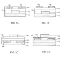
- FIG. 1A there is schematically illustrated an organic field effect transistor (OTFT) showing the relative positions of the active layers of such a device in “bottom contact mode.”
- OTFT organic field effect transistor
- the drain and source electrodes are deposited onto the gate dielectric layer prior to depositing the active organic semiconductor layer onto the source and drain electrodes and any remaining exposed gate dielectric layer.
- a substrate 112 is in contact with a gate electrode 102 and an insulating layer 104 on top of which the source electrode 106 and drain electrode 108 are deposited.
- an organic semiconductor layer 110 comprising an electroactive compound of Formula I or Formula II.
- Figure 1B is a schematic diagram of an OTFT showing the relative positions of the active layers of such a device in top contact mode. (In “top contact mode,” the drain and source electrodes of an OTFT are deposited on top of the active organic semiconductor layer.)
- Figure 1C is a schematic diagram of OTFT showing the relative positions of the active layers of such a device in bottom contact mode with the gate at the top.
- Figure 1D is a schematic diagram of an OTFT showing the relative positions of the active layers of such a device in top contact mode with the gate at the top.
- the substrate can comprise inorganic glasses, ceramic foils, polymeric materials (for example, acrylics, epoxies, polyamides, polycarbonates, polyimides, polyketones, poly(oxy-1, 4-phenyleneoxy-1,4-phenylenecarbonyl-1,4-phenylene) (sometimes referred to as poly(ether ether ketone) or PEEK), polynorbornenes, polyphenyleneoxides, poly(ethylene naphthalenedicarboxylate) (PEN), poly(ethylene terephthalate) (PET), poly(phenylene sulfide) (PPS)), filled polymeric materials (for example, fiber-reinforced plastics (FRP)), and/or coated metallic foils.
- polymeric materials for example, acrylics, epoxies, polyamides, polycarbonates, polyimides, polyketones, poly(oxy-1, 4-phenyleneoxy-1,4-phenylenecarbonyl-1,4-phenylene) (sometimes referred to as poly
- the thickness of the substrate can be from about 10 micrometers to over 10 millimeters; for example, from about 50 to about 100 micrometers for a flexible plastic substrate; and from about 1 to about 10 millimeters for a rigid substrate such as glass or silicon.
- a substrate supports the OTFT during manufacturing, testing, and/or use.
- the substrate can provide an electrical function such as bus line connection to the source, drain, and electrodes and the circuits for the OTFT.
- the gate electrode can be a thin metal film, a conducting polymer film, a conducting film made from conducting ink or paste or the substrate itself, for example heavily doped silicon.
- suitable gate electrode materials include aluminum, gold, chromium, indium tin oxide, conducting polymers such as polystyrene sulfonate-doped poly(3,4-ethylenedioxythiophene) (PSS-PEDOT), conducting ink/paste comprised of carbon black/graphite or colloidal silver dispersion in polymer binders.
- PSS-PEDOT polystyrene sulfonate-doped poly(3,4-ethylenedioxythiophene)
- conducting ink/paste comprised of carbon black/graphite or colloidal silver dispersion in polymer binders.
- the same material can provide the gate electrode function and also provide the support function of the substrate.
- doped silicon can function as the gate electrode and support the OTFT.
- the gate electrode can be prepared by vacuum evaporation, sputtering of metals or conductive metal oxides, coating from conducting polymer solutions or conducting inks by spin coating, casting or printing.
- the thickness of the gate electrode can be, for example, from about 10 to about 200 nanometers for metal films and from about 1 to about 10 micrometers for polymer conductors.
- the source and drain electrodes can be fabricated from materials that provide a low resistance ohmic contact to the semiconductor layer, such that the resistance of the contact between the semiconductor layer and the source and drain electrodes is less than the resistance of the semiconductor layer.
- Channel resistance is the conductivity of the semiconductor layer. Typically, the resistance should be less than the channel resistance.
- Typical materials suitable for use as source and drain electrodes include aluminum, barium, calcium, chromium, gold, silver, nickel, palladium, platinum, titanium, and alloys thereof; carbon nanotubes; conducting polymers such as polyaniline and poly(3,4-ethylenedioxythiophene)/poly-(styrene sulfonate) (PEDOT:PSS); dispersions of carbon nanotubes in conducting polymers; dispersions of a metal in a conducting polymer; and multilayers thereof. Some of these materials are appropriate for use with n-type semiconductor materials and others are appropriate for use with p- type semiconductor materials, as is known to those skilled in the art.
- Typical thicknesses of source and drain electrodes are about, for example, from about 40 nanometers to about 1 micrometer. In some embodiments, the thickness is about 100 to about 400 nanometers.
- the insulating layer comprises an inorganic material film or an organic polymer film.
- inorganic materials suitable as the insulating layer include aluminum oxides, silicon oxides, tantalum oxides, titanium oxides, silicon nitrides, barium titanate, barium strontium titanate, barium zirconate titanate, zinc selenide, and zinc sulfide.
- alloys, combinations, and multilayers of the aforesaid materials can be used for the insulating layer.
- Illustrative examples of organic polymers for the insulating layer include polyesters, polycarbonates, poly(vinyl phenol), polyimides, polystyrene, poly(methacrylate)s, poly(acrylate)s, epoxy resins and blends and multilayers thereof.
- the thickness of the insulating layer is, for example from about 10 nanometers to about 500 nanometers, depending on the dielectric constant of the dielectric material used. For example, the thickness of the insulating layer can be from about 100 nanometers to about 500 nanometers.
- the insulating layer, the gate electrode, the semiconductor layer, the source electrode, and the drain electrode are formed in any sequence as long as the gate electrode and the semiconductor layer both contact the insulating layer, and the source electrode and the drain electrode both contact the semiconductor layer.
- the phrase "in any sequence" includes sequential and simultaneous formation.
- the source electrode and the drain electrode can be formed simultaneously or sequentially.
- the gate electrode, the source electrode, and the drain electrode can be provided using known methods such as physical vapor deposition (for example, thermal evaporation or sputtering) or ink jet printing.
- the patterning of the electrodes can be accomplished by known methods such as shadow masking, additive photolithography, subtractive photolithography, printing, microcontact printing, and pattern coating.
- electrodes 106 and 108 which form channels for source and drain respectively, can be created on the silicon dioxide layer using a photolithographic process.
- a semiconductor layer 110 is then deposited over the surface of electrodes 106 and 108 and layer 104.
- semiconductor layer 110 comprises one or more compounds represented by Formula I or Formula II.
- the semiconductor layer 110 can be deposited by various techniques known in the art. These techniques include thermal evaporation, chemical vapor deposition, thermal transfer, ink-jet printing and screenprinting. Dispersion thin film coating techniques for deposition include spin coating, doctor blade coating, drop casting and other known techniques.
- layer 110 is deposited on layer 104 before the fabrication of electrodes 106 and 108.
- the present invention also relates to an electronic device comprising at least one active layer positioned between two electrical contact layers, wherein the at least one active layer of the device includes a new compound having Formula I or Formula II.
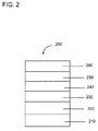
- the device 200 has a first electrical contact layer, an anode layer 210 and a second electrical contact layer, a cathode layer 260, and a photoactive layer 240 between them.
- Adjacent to the anode may be a hole injection layer 220.
- Adjacent to the hole injection layer may be a hole transport layer 230, comprising hole transport material.
- Adjacent to the cathode may be an electron transport layer 250, comprising an electron transport material.
- Devices may use one or more additional hole injection or hole transport layers (not shown) next to the anode 210 and/or one or more additional electron injection or electron transport layers (not shown) next to the cathode 260.
- Layers 220 through 250 are individually and collectively referred to as the active layers.
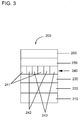
- the photoactive layer 240 is pixellated, as shown in Figure 3 .
- Layer 240 is divided into pixel or subpixel units 241, 242, and 243 which are repeated over the layer.
- Each of the pixel or subpixel units represents a different color.
- the subpixel units are for red, green, and blue. Although three subpixel units are shown in the figure, two or more than three may be used.
- the different layers have the following range of thicknesses: anode 210, 500-5000 A, in one embodiment 1000-2000 A; hole injection layer 220, 50-2000 A, in one embodiment 200-1000 A; hole transport layer 230, 50-2000 A, in one embodiment 200-1000 A; electroactive layer 240, 10-2000 A, in one embodiment 100-1000 A; layer 250, 50-2000 A, in one embodiment 100-1000 A; cathode 260, 200-10000 A, in one embodiment 300-5000 A.
- the location of the electron-hole recombination zone in the device, and thus the emission spectrum of the device can be affected by the relative thickness of each layer.
- the desired ratio of layer thicknesses will depend on the exact nature of the materials used.
- the devices have additional layers to aid in processing or to improve functionality.
- the photoactive layer 240 can be a light-emitting layer that is activated by an applied voltage (such as in a light-emitting diode or light-emitting electrochemical cell), or a layer of material that responds to radiant energy and generates a signal with or without an applied bias voltage (such as in a photodetector).
- an applied voltage such as in a light-emitting diode or light-emitting electrochemical cell
- a layer of material that responds to radiant energy and generates a signal with or without an applied bias voltage
- Examples of photodetectors include photoconductive cells, photoresistors, photoswitches, phototransistors, and phototubes, and photovoltaic cells, as these terms are described in Markus, John, Electronics and Nucleonics Dictionary, 470 and 476 (McGraw-Hill, Inc. 1966 ).
- Devices with light-emitting layers may be used to form displays or for lighting applications, such as white light luminaires.
- One or more of the new electroactive compounds described herein may be present in one or more of the active layers of a device.
- the new electroactive compounds having Formula I or Formula II are useful as host materials for photoactive dopant materials in photoactive layer 240. It has been found that when these compounds are used by themselves or in conjunction with other cohosts, they can provide improved efficiency and lifetime in OLED devices. It has been discovered through calculations that these compounds have high triplet energies and HOMO and LUMO levels appropriate for charge transport, making them excellent host materials for organometallic emitters.
- the new electroactive compounds are useful as electron transport materials in layer 250.
- the photoactive layer 240 comprises the electroactive composition described above.
- the dopant is an organometallic material.
- the organometallic material is a complex of Ir or Pt.
- the organometallic material is a cyclometallated complex of Ir.
- the photoactive layer comprises (a) a host material having Formula I or Formula II and (b) one or more dopants. In some embodiments, the photoactive layer comprises (a) a host material having Formula I or Formula II and (b) an organometallic electroluminescent dopant. In some embodiments, the photoactive layer comprises (a) a host material having Formula I or Formula II, (b) a photoactive dopant, and (c) a second host material. In some embodiments, the photoactive layer comprises (a) a host material having Formula I or Formula II, (b) an organometallic complex of Ir or Pt, and (c) a second host material. In some embodiments, the photoactive layer comprises (a) a host material having Formula I or Formula II, (b) a cyclometallated complex of Ir, and (c) a second host material.
- the photoactive layer consists essentially of (a) a host material having Formula I or Formula II and (b) one or more dopants. In some embodiments, the photoactive layer consists essentially of (a) a host material having Formula I or Formula II and (b) an organometallic electroluminescent dopant. In some embodiments, the photoactive layer consists essentially of (a) a host material having Formula I or Formula II, (b) a photoactive dopant, and (c) a second host material. In some embodiments, the photoactive layer consists essentially of (a) a host material having Formula I or Formula II, (b) an organometallic complex of Ir or Pt, and (c) a second host material. In some embodiments, the photoactive layer consists essentially of (a) a host material having Formula I or Formula II, (b) a cyclometallated complex of Ir, and (c) a second host material.
- the photoactive layer consists essentially of (a) a host material having Formula I or Formula II, wherein the compound is deuterated, and (b) one or more dopants. In some embodiments, the photoactive layer consists essentially of a host material having Formula I or Formula II, wherein the compound is deuterated, and (b) an organometallic electroluminescent dopant. In some embodiments, the photoactive layer consists essentially of (a) a host material having Formula I or Formula II, wherein the compound is deuterated, (b) a photoactive dopant, and (c) a second host material.
- the photoactive layer consists essentially of a host material having Formula I or Formula II, wherein the compound is deuterated, (b) an organometallic complex of Ir or Pt, and (c) a second host material.
- the photoactive layer consists essentially of (a) a host material having Formula I or Formula II, wherein the compound is deuterated a host material having Formula I or Formula II, wherein the compound is deuterated, (b) a cyclometallated complex of Ir, and (c) a second host material.
- the deuterated compound of Formula I or Formula II is at least 10% deuterated; in some embodiments, at least 50% deuterated.
- the second host material is deuterated.
- the second host material is at least 10% deuterated; in some embodiments, at least 50% deuterated.
- the new compounds of Formulae I and II are useful as electron transport materials in layer 250.
- the compounds can be used alone, or in combination with another electron transport material.
- the electron transport layer consists essentially of a new compound of Formula I or II.
- Examples of other electron transport materials which can be used alone or in combination with the new compounds include, but are not limited to, metal chelated oxinoid compounds, including metal quinolate derivatives such as tris(8-hydroxyquinolato)aluminum (AIQ), bis(2-methyl-8-quinolinolato)(p-phenylphenolato) aluminum (BAlq), tetrakis-(8-hydroxyquinolato)hafnium (HfQ) and tetrakis-(8-hydroxyquinolato)zirconium (ZrQ); and azole compounds such as 2- (4-biphenylyl)-5-(4-t-butylphenyl)-1,3,4-oxadiazole (PBD), 3-(4-biphenylyl)-4-phenyl-5-(4-t-butylphenyl)-1,2,4-triazole (TAZ), and 1,3,5-tri(phenyl-2-benzimidazole)benzene (TPBI); qui
- the electron transport material is selected from the group consisting of metal quinolates and phenanthroline derivatives.
- the electron transport layer further comprises an n-dopant.
- N-dopant materials are well known.
- the other layers in the device can be made of any materials that are known to be useful in such layers.
- the anode 210 is an electrode that is particularly efficient for injecting positive charge carriers. It can be made of, for example, materials containing a metal, mixed metal, alloy, metal oxide or mixed-metal oxide, or it can be a conducting polymer, or mixtures thereof. Suitable metals include the Group 11 metals, the metals in Groups 4-6, and the Group 8-10 transition metals. If the anode is to be light-transmitting, mixed-metal oxides of Groups 12, 13 and 14 metals, such as indium-tin-oxide, are generally used.
- the anode 210 can also comprise an organic material such as polyaniline as described in " Flexible light-emitting diodes made from soluble conducting polymer," Nature vol. 357, pp 477-479 (11 June 1992 ). At least one of the anode and cathode is desirably at least partially transparent to allow the generated light to be observed.
- the hole injection layer 220 comprises hole injection material and may have one or more functions in an organic electronic device, including but not limited to, planarization of the underlying layer, charge transport and/or charge injection properties, scavenging of impurities such as oxygen or metal ions, and other aspects to facilitate or to improve the performance of the organic electronic device.
- Hole injection materials may be polymers, oligomers, or small molecules. They may be vapour deposited or deposited from liquids which may be in the form of solutions, dispersions, suspensions, emulsions, colloidal mixtures, or other compositions.
- the hole injection layer can be formed with polymeric materials, such as polyaniline (PANI) or polyethylenedioxythiophene (PEDOT), which are often doped with protonic acids.
- the protonic acids can be, for example, poly(styrenesulfonic acid), poly(2-acrylamido-2-methyl-1-propanesulfonic acid), and the like.
- the hole injection layer can comprise charge transfer compounds, and the like, such as copper phthalocyanine and the tetrathiafulvalene-tetracyanoquinodimethane system (TTF-TCNQ).
- charge transfer compounds such as copper phthalocyanine and the tetrathiafulvalene-tetracyanoquinodimethane system (TTF-TCNQ).
- the hole injection layer comprises at least one electrically conductive polymer and at least one fluorinated acid polymer. In some embodiments, the hole injection layer comprises an electrically conductive polymer doped with a fluorinated acid polymer. materials have been described in, for example, published U.S. patent applications US 2004/0102577 , US 2004/0127637 , US 2005/0205860 , and published PCT application WO 2009/018009 .
- hole transport materials for layer 230 have been summarized for example, in Kirk-Othmer Encyclopedia of Chemical Technology, Fourth Edition, Vol. 18, p. 837-860, 1996, by Y. Wang . Both hole transporting molecules and polymers can be used. Commonly used hole transporting molecules are: N,N'-diphenyl-N,N'-bis(3-methylphenyl)-[1,1'-biphenyl]-4,4'-diamine (TPD), 1,1-bis[(di-4-tolylamino) phenyl]cyclohexane (TAPC), N,N'-bis(4-methylphenyl)-N,N'-bis(4-ethylphenyl)-[1,1'-(3,3'-dimethyl)biphenyl]-4,4'-diamine (ETPD), tetrakis-(3-methylphenyl)-N,N,N',N'-2,5-phenylenediamine (PDA),
- hole transporting polymers are polyvinylcarbazole, (phenylmethyl)-polysilane, and polyaniline. It is also possible to obtain hole transporting polymers by doping hole transporting molecules such as those mentioned above into polymers such as polystyrene and polycarbonate. In some cases, triarylamine polymers are used, especially triarylamine-fluorene copolymers. In some cases, the polymers and copolymers are crosslinkable. In some embodiments, the hole transport layer further comprises a p-dopant. In some embodiments, the hole transport layer is doped with a p-dopant.
- p-dopants include, but are not limited to, tetrafluorotetracyanoquinodimethane (F4-TCNQ) and perylene-3,4,9,10-tetracarboxylic-3,4,9,10-dianhydride (PTCDA).
- F4-TCNQ tetrafluorotetracyanoquinodimethane
- PTCDA perylene-3,4,9,10-tetracarboxylic-3,4,9,10-dianhydride
- the cathode 260 is an electrode that is particularly efficient for injecting electrons or negative charge carriers.
- the cathode can be any metal or nonmetal having a lower work function than the anode.
- Materials for the cathode can be selected from alkali metals of Group 1 (e.g., Li, Cs), the Group 2 (alkaline earth) metals, the Group 12 metals, including the rare earth elements and lanthanides, and the actinides. Materials such as aluminum, indium, calcium, barium, samarium and magnesium, as well as combinations, can be used.
- Li- or Cs-containing organometallic compounds, LiF, CsF, and Li 2 O can also be deposited between the organic layer and the cathode layer to lower the operating voltage.
- anode 210 there can be a layer (not shown) between the anode 210 and hole injection layer 220 to control the amount of positive charge injected and/or to provide band-gap matching of the layers, or to function as a protective layer.
- Layers that are known in the art can be used, such as copper phthalocyanine, silicon oxy-nitride, fluorocarbons, silanes, or an ultra-thin layer of a metal, such as Pt.
- some or all of anode layer 210, active layers 220, 230, 240, and 250, or cathode layer 260 can be surface-treated to increase charge carrier transport efficiency.
- the choice of materials for each of the component layers is preferably determined by balancing the positive and negative charges in the emitter layer to provide a device with high electroluminescence efficiency.
- each functional layer can be made up of more than one layer.
- the device can be prepared by a variety of techniques, including sequential vapor deposition of the individual layers on a suitable substrate.
- Substrates such as glass, plastics, and metals can be used.
- Conventional vapor deposition techniques can be used, such as thermal evaporation, chemical vapor deposition, and the like.
- the organic layers can be applied from solutions or dispersions in suitable solvents, using conventional coating or printing techniques, including but not limited to spin-coating, dip-coating, roll-to-roll techniques, ink-jet printing, screenprinting, gravure printing and the like.
- the device is fabricated by liquid deposition of the buffer layer, the hole transport layer, and the photoactive layer, and by vapor deposition of the anode, the electron transport layer, an electron injection layer and the cathode.
- the HOMO (highest occupied molecular orbital) of the hole transport material desirably aligns with the work function of the anode
- the LUMO (lowest un-occupied molecular orbital) of the electron transport material desirably aligns with the work function of the cathode.
- Chemical compatibility and sublimation temperature of the materials may also be considerations in selecting the electron and hole transport materials.
- the efficiency of devices made with the new compounds described herein can be further improved by optimizing the other layers in the device.
- more efficient cathodes such as Ca, Ba or LiF can be used.
- Shaped substrates and novel hole transport materials that result in a reduction in operating voltage or increase quantum efficiency are also applicable.
- Additional layers can also be added to tailor the energy levels of the various layers and facilitate electroluminescence.
- This example illustrates the synthesis of Compound 1, 2,4,8,10-tetraphenyl-quino[8,7-h]quinoline.
- Eaton's Reagent (210 mL, 7.7 w % P 2 O 5 in methanesulfonic acid) was freshly prepared prior to the reaction.
- Phosphorus pentoxide 24.06 g
- 195 mL methanesulfonic acid (288.44g) were combined in the reaction flask under nitrogen and heated for 1 hour at 70°C before cooling to room temperature.
- 1,5-Bis(ethyl benzoylacetanilide)naphthalene (23.5 g, 43.6 mmol) was added to the solution and the mixture heated to 50°C under nitrogen for 34 hours before cooling to ambient temperature.
- Water 400mL was slowly added and the resulting mixture was then neutralized using 50% NaOH solution. This mixture was stirred for 1 hour before filtering, and the collected precipitate was rinsed with methanol before drying under vacuum to yield 18.55g (96.5% yield) of an off-white powder.
- Phosphorus (V) oxychloride (165mL) and substrate (18.5 g, 44.7 mmol) were combined in the reaction flask under nitrogen and warmed to reflux temperature for 7 hours before cooling back to room temperature.
- the mixture was slowly added to 4L cold water and stirred for a further 30 minutes.
- the mixture was then neutralized with 50% NaOH solution.
- the precipitate was filtered and rinsed with 1 L water, followed by 500 mL methanol.
- the collected solid was dried under vacuum to yield 19.1 g of crude product. This material was then suspended in toluene and the slurry mixture warmed to reflux temperature with stirring. The solids never fully dissolved into the hot toluene.
- the mixture was allowed to come back to room temperature after 4 hours heating at reflux.
- Phenylboronic acid (3.38 g, 27.7 mmol), 1,7-dichloro-4,10-diazachrysene (2.50 g, 5.50 mmol), potassium carbonate (19.1 g, 138 mmol) dissolved into 70mL water, and 1,4-dioxane (70 mL) were combined in a flask and sparged with nitrogen for 45 minutes.
- Tris (dibenzilineacetone)dipalladium(0) (0.142 g, 0.140 mmol
- tricyclohosphine 0.112 g, 0.550 mmol
- the reaction mixture was then cooled to room temperature and the product extracted with chloroform and the solution dried with magnesium sulfate before concentrating under reduced pressure.
- the crude product was then purified by column chromatography using silica gel and 100% chloroform as eluent. The product fractions were collected and concentrated under reduced pressure to afford an off-white solid. This residue was then recrystallized from hot toluene ( ⁇ 400mL) to yield 1.82g (61.6% yield).
- the product underwent vapor sublimation as a final purification step.
- the structure was confirmed by 1 H NMR using chlorobenzene- d 5 at 80°C.
- This example illustrates the use of the new compounds in the electron transport layer of an OLED device.
- HIJ-1 Indium Tin Oxide (ITO)
- 50 nm hole injection layer HIJ-1, 50 nm.
- HIJ-1 is an aqueous dispersion of an electrically conductive polymer and a polymeric fluorinated sulfonic acid. Such materials have been described in, for example, published U.S. patent applications US 2004/0102577 , US 2004/0127637 , and US 2005/0205860 , and published PCT application WO 2009/018009 .
- hole transport layer HT-1 (20 nm).
- HT-1 is a hole transport material which is a triarylamine polymer.
- H1 is a deuterated diarylanthracene.
- the non-deuterated analogs of such materials have been previously disclosed as blue host materials in, for example, published U.S. patent application no. US 2007-0088185 (Idemitsu).
- E1 is a bis(diarylamino)chrysene.
- the electron transport layer was tetrakis (8-hydroxyquinoline)zirconium ("ZrQ4").
- the electron transport layer was Compound 1.
- OLED devices were fabricated by a combination of solution processing and thermal evaporation techniques.
- Patterned indium tin oxide (ITO) coated glass substrates from Thin Film Devices, Inc were used. These ITO substrates are based on Corning 1737 glass coated with ITO having a sheet resistance of 30 ohms/square and 80% light transmission.
- the patterned ITO substrates were cleaned ultrasonically in aqueous detergent solution and rinsed with distilled water.
- the patterned ITO was subsequently cleaned ultrasonically in acetone, rinsed with isopropanol, and dried in a stream of nitrogen.
- ITO substrates were treated with UV ozone for 10 minutes.
- an aqueous dispersion of HIJ-1 was spin-coated over the ITO surface and heated to remove solvent.
- the substrates were then spin-coated with a toluene solution of HT-1, and then heated to remove solvent.
- the substrates were masked and placed in a vacuum chamber. After cooling the substrates were spin-coated with a methyl benzoate solution of the host and dopant, and heated to remove solvent.
- the substrates were masked and placed in a vacuum chamber.
- a layer of electron transport material was deposited by thermal evaporation, followed by a layer of CsF.
- Masks were then changed in vacuo and a layer of Al was deposited by thermal evaporation.
- the chamber was vented, and the devices were encapsulated using a glass lid, dessicant, and UV curable epoxy.
- the OLED samples were characterized by measuring their (1) current-voltage (I-V) curves, (2) electroluminescence radiance versus voltage, and (3) electroluminescence spectra versus voltage. All three measurements were performed at the same time and controlled by a computer.
- the current efficiency of the device at a certain voltage is determined by dividing the electroluminescence radiance of the LED by the current density needed to run the device.
- the unit is a cd/A.
- the color coordinates were determined using either a Minolta CS-100 meter or a Photoresearch PR-705 meter.
Landscapes
- Chemical & Material Sciences (AREA)
- Organic Chemistry (AREA)
- Engineering & Computer Science (AREA)
- Materials Engineering (AREA)
- Physics & Mathematics (AREA)
- Optics & Photonics (AREA)
- Spectroscopy & Molecular Physics (AREA)
- Microelectronics & Electronic Packaging (AREA)
- Electroluminescent Light Sources (AREA)
- Nitrogen Condensed Heterocyclic Rings (AREA)
- Thin Film Transistor (AREA)
- Pyridine Compounds (AREA)
Claims (14)
- Verbindung, die die Formel I oder Formel II

 Ar1-Ar4 gleich oder verschieden sind und Kohlenwasserstoffaryle, N-Heterocyclen oder deuterierte Analoga davon sind.
 - Verbindung nach Anspruch 1, wobei mindestens eines von Ar1-Ar4 einen Substituenten aufweist, der Alkyl, Aryl, Silyl, Diarylamin, Carbazol oder ein deuteriertes Analogon davon ist.
- Verbindung nach Anspruch 1, wobei Ar1-Ar4 die Formel a
 R1 bei jedem Vorkommen gleich oder verschieden ist und D, Aryl, Alkyl, Silyl, Diarylamino, Carbazolyl oder ein deuteriertes Analogon davon ist;a bei jedem Vorkommen gleich oder verschieden ist und eine ganze Zahl von 0 - 4 ist;b eine ganze Zahl von 0 - 5 ist; undm eine ganze Zahl von 1 bis 5 ist.
 - Verbindung nach Anspruch 1, wobei Ar1-Ar4 die Formel b
 R1 H, D, Aryl, Alkyl, Silyl, Diarylamino, Carbazolyl oder ein deuteriertes Analogon davon ist undm eine ganze Zahl von 1 bis 5 ist;oder deuteriertes Analogon davon.
 - Verbindung nach Anspruch 1, wobei Ar1-Ar4 die Formel c

R1 H, D, Aryl, Alkyl, Silyl, Diarylamino, Carbazolyl oder ein deuteriertes Analogon davon ist,
oder deuteriertes Analogon davon. - Verbindung nach Anspruch 1, wobei eines oder mehrere von Ar1-Ar4 Phenyl, Biphenyl, Terphenyl, Naphthyl, Phenylnaphthyl, Naphthylphenyl, Pyridin, Pyrimidin, Triazin oder ein deuteriertes Analogon davon ist.
- Verbindung nach Anspruch 6, wobei mindestens eines von Ar1-Ar4 mit Diarylamino, Carbazol oder einem deuterierten Analogon davon substituiert ist.
- Verbindung nach Anspruch 1 ausgewählt unter Verbindung 1 bis Verbindung 8 Verbindung 1


- Zusammensetzung umfassend (a) eine Wirtsverbindung. die die Formel I oder Formel II, wie in einem der vorhergehenden Ansprüche definiert, aufweist, und (b) ein Dotiermittel, das der Elektrolumineszenz fähig ist, die ein Emissionsmaximum zwischen 380 und 750 aufweist.
- Elektronische Vorrichtung, die mindestens eine Schicht aufweist, die die Verbindung der Formel I oder Formel II, wie in einem der Ansprüche 1 - 8 definiert, umfasst.
- Vorrichtung nach Anspruch 10, umfassend eine Anode, eine Lochinjektionsschicht, eine photoaktive Schicht, eine Elektronentransportschicht und eine Kathode, wobei mindestens eine von der photoaktiven Schicht und der Elektronentransportschicht eine Verbindung der Formel I oder Formel II umfasst.
- Vorrichtung nach Anspruch 11, wobei die photoaktive Schicht (a) ein Wirtsmaterial, das die Formel I oder Formel II aufweist, und (b) ein organometallisches elektrolumineszierendes Dotiermittel umfasst.
- Vorrichtung nach Anspruch 12, wobei die Lochinjektionsschicht mindestens ein elektrisch leitfähiges Polymer und mindestens ein fluoriertes saures Polymer umfasst.
- Vorrichtung nach Anspruch 10, wobei die Elektronentransportschicht eine Verbindung umfasst, die die Formel I oder Formel II aufweist.
Applications Claiming Priority (2)
| Application Number | Priority Date | Filing Date | Title |
|---|---|---|---|
| US42337210P | 2010-12-15 | 2010-12-15 | |
| PCT/US2011/064360 WO2012082593A2 (en) | 2010-12-15 | 2011-12-12 | Electroactive material and devices made with such materials |
Publications (2)
| Publication Number | Publication Date |
|---|---|
| EP2651942A2 EP2651942A2 (de) | 2013-10-23 |
| EP2651942B1 true EP2651942B1 (de) | 2016-03-16 |
Family
ID=45496261
Family Applications (1)
| Application Number | Title | Priority Date | Filing Date |
|---|---|---|---|
| EP11808993.7A Not-in-force EP2651942B1 (de) | 2010-12-15 | 2011-12-12 | Elektroaktive 1,7- und 4,10-diazachrysenderivate und aus solchen materialien hergestellte vorrichtungen |
Country Status (6)
| Country | Link |
|---|---|
| US (1) | US9269909B2 (de) |
| EP (1) | EP2651942B1 (de) |
| JP (1) | JP5837611B2 (de) |
| KR (1) | KR101539156B1 (de) |
| TW (1) | TW201226410A (de) |
| WO (1) | WO2012082593A2 (de) |
Families Citing this family (10)
| Publication number | Priority date | Publication date | Assignee | Title |
|---|---|---|---|---|
| KR101971198B1 (ko) * | 2011-10-19 | 2019-04-23 | 삼성디스플레이 주식회사 | 헤테로시클릭 화합물, 이를 포함하는 유기 발광 소자 및 평판 표시 장치 |
| TW201339138A (zh) * | 2012-01-20 | 2013-10-01 | Univ Southern California | 作為用於有機電子裝置之新穎n-型材料之氮雜-并苯之合成 |
| JP6463696B2 (ja) * | 2013-02-25 | 2019-02-06 | イー・アイ・デュポン・ドウ・ヌムール・アンド・カンパニーE.I.Du Pont De Nemours And Company | ジアザクリセン誘導体を含む電子デバイス |
| WO2018043725A1 (ja) * | 2016-09-02 | 2018-03-08 | 国立大学法人東京工業大学 | 有機半導体材料及び有機化合物並びに有機半導体装置 |
| KR102658368B1 (ko) | 2016-12-09 | 2024-04-18 | 삼성디스플레이 주식회사 | 축합환 화합물 및 이를 포함한 유기 발광 소자 |
| CN109134456B (zh) * | 2017-06-13 | 2020-11-03 | 北京鼎材科技有限公司 | 一种并喹啉类衍生物及其应用和有机电致发光器件 |
| US10923660B2 (en) | 2017-09-29 | 2021-02-16 | Beijing Summer Sprout Technology Co., Ltd. | Liquid formulation and a method for making electronic devices by solution process |
| TWI731616B (zh) * | 2020-03-09 | 2021-06-21 | 財團法人紡織產業綜合研究所 | 電致發光線 |
| CN115894484B (zh) * | 2022-12-02 | 2024-03-19 | 烟台九目化学股份有限公司 | 一种异喹啉并喹啉类化合物及其制备方法和应用 |
| CN117038759B (zh) * | 2023-09-23 | 2024-04-19 | 河北大学 | 一种以炭黑导电薄膜作为空穴传输层的晶硅太阳能电池 |
Family Cites Families (21)
| Publication number | Priority date | Publication date | Assignee | Title |
|---|---|---|---|---|
| US7476452B2 (en) | 2000-06-30 | 2009-01-13 | E. I. Du Pont De Nemours And Company | Electroluminescent iridium compounds with fluorinated phenylpyridine ligands, and devices made with such compounds |
| US6670645B2 (en) | 2000-06-30 | 2003-12-30 | E. I. Du Pont De Nemours And Company | Electroluminescent iridium compounds with fluorinated phenylpyridines, phenylpyrimidines, and phenylquinolines and devices made with such compounds |
| US7166368B2 (en) | 2001-11-07 | 2007-01-23 | E. I. Du Pont De Nemours And Company | Electroluminescent platinum compounds and devices made with such compounds |
| EP2299785A1 (de) | 2001-12-26 | 2011-03-23 | E. I. du Pont de Nemours and Company | Iridiumverbindungen |
| JP4161262B2 (ja) | 2002-06-26 | 2008-10-08 | ソニー株式会社 | 有機電界発光素子、及びそれを用いた発光又は表示装置 |
| US6963005B2 (en) | 2002-08-15 | 2005-11-08 | E. I. Du Pont De Nemours And Company | Compounds comprising phosphorus-containing metal complexes |
| AU2003275203A1 (en) | 2002-09-24 | 2004-04-19 | E.I. Du Pont De Nemours And Company | Water dispersible polythiophenes made with polymeric acid colloids |
| CN1681869B (zh) | 2002-09-24 | 2010-05-26 | E.I.内穆尔杜邦公司 | 用于电子器件用聚合物酸胶体制成的可水分散的聚苯胺 |
| US6875524B2 (en) | 2003-08-20 | 2005-04-05 | Eastman Kodak Company | White light-emitting device with improved doping |
| JPWO2005081587A1 (ja) | 2004-02-19 | 2008-01-17 | 出光興産株式会社 | 白色系有機エレクトロルミネッセンス素子 |
| US7351358B2 (en) | 2004-03-17 | 2008-04-01 | E.I. Du Pont De Nemours And Company | Water dispersible polypyrroles made with polymeric acid colloids for electronics applications |
| JPWO2006104044A1 (ja) | 2005-03-28 | 2008-09-04 | 出光興産株式会社 | アントリルアリーレン誘導体、有機エレクトロルミネッセンス素子用材料、及びそれを用いた有機エレクトロルミネッセンス素子 |
| KR100788254B1 (ko) | 2005-08-16 | 2007-12-27 | (주)그라쎌 | 녹색 발광 화합물 및 이를 발광재료로서 채용하고 있는발광소자 |
| EP2173811A1 (de) | 2007-07-27 | 2010-04-14 | E. I. du Pont de Nemours and Company | Wässrige dispersionen aus elektrisch leitenden polymeren mit anorganischen nanopartikeln |
| US8063399B2 (en) | 2007-11-19 | 2011-11-22 | E. I. Du Pont De Nemours And Company | Electroactive materials |
| US20110259807A1 (en) | 2008-09-25 | 2011-10-27 | Metawater Co., Ltd. | Filtering and condensing apparatus of suction type |
| EP2432849B1 (de) * | 2009-05-19 | 2015-02-25 | E. I. du Pont de Nemours and Company | Chrysenverbindungen für leuchtanwendungen |
| JP5567675B2 (ja) * | 2009-08-13 | 2014-08-06 | イー・アイ・デュポン・ドウ・ヌムール・アンド・カンパニー | クリセン誘導体材料 |
| JP5523016B2 (ja) * | 2009-08-20 | 2014-06-18 | キヤノン株式会社 | 複素環化合物及びこれを用いた有機発光素子 |
| JP5523021B2 (ja) * | 2009-08-25 | 2014-06-18 | キヤノン株式会社 | 複素環化合物及びこれを用いた有機発光素子 |
| KR101971198B1 (ko) * | 2011-10-19 | 2019-04-23 | 삼성디스플레이 주식회사 | 헤테로시클릭 화합물, 이를 포함하는 유기 발광 소자 및 평판 표시 장치 |
-
2011
- 2011-12-12 WO PCT/US2011/064360 patent/WO2012082593A2/en not_active Ceased
- 2011-12-12 EP EP11808993.7A patent/EP2651942B1/de not_active Not-in-force
- 2011-12-12 JP JP2013544641A patent/JP5837611B2/ja active Active
- 2011-12-12 US US13/989,296 patent/US9269909B2/en active Active
- 2011-12-12 KR KR1020137018270A patent/KR101539156B1/ko active Active
- 2011-12-14 TW TW100146127A patent/TW201226410A/zh unknown
Also Published As
| Publication number | Publication date |
|---|---|
| JP2014506246A (ja) | 2014-03-13 |
| KR101539156B1 (ko) | 2015-07-23 |
| KR20140040686A (ko) | 2014-04-03 |
| WO2012082593A2 (en) | 2012-06-21 |
| JP5837611B2 (ja) | 2015-12-24 |
| TW201226410A (en) | 2012-07-01 |
| US9269909B2 (en) | 2016-02-23 |
| US20130240866A1 (en) | 2013-09-19 |
| EP2651942A2 (de) | 2013-10-23 |
| WO2012082593A3 (en) | 2012-08-16 |
Similar Documents
| Publication | Publication Date | Title |
|---|---|---|
| US9496506B2 (en) | Deuterated compounds for electronic applications | |
| US20130264560A1 (en) | Triazine derivatives for electronic applications | |
| KR102158326B1 (ko) | 전자적 응용을 위한 전기활성 조성물 | |
| EP2651942B1 (de) | Elektroaktive 1,7- und 4,10-diazachrysenderivate und aus solchen materialien hergestellte vorrichtungen | |
| US8617720B2 (en) | Electroactive composition and electronic device made with the composition | |
| US20130256646A1 (en) | Electronic device including a pyrimidine compound | |
| WO2012087955A1 (en) | Compositions for electronic applications | |
| US9966542B2 (en) | Electroactive materials | |
| US20120187383A1 (en) | Electroactive compound and composition and electronic device made with the composition | |
| US10804473B2 (en) | Electron transport materials for electronic applications | |
| US9748497B2 (en) | Electronic device including a diazachrysene derivative | |
| US9876174B2 (en) | Electronic device including a fluoranthene derivative |
Legal Events
| Date | Code | Title | Description |
|---|---|---|---|
| PUAI | Public reference made under article 153(3) epc to a published international application that has entered the european phase |
Free format text: ORIGINAL CODE: 0009012 |
|
| 17P | Request for examination filed |
Effective date: 20130418 |
|
| AK | Designated contracting states |
Kind code of ref document: A2 Designated state(s): AL AT BE BG CH CY CZ DE DK EE ES FI FR GB GR HR HU IE IS IT LI LT LU LV MC MK MT NL NO PL PT RO RS SE SI SK SM TR |
|
| DAX | Request for extension of the european patent (deleted) | ||
| 17Q | First examination report despatched |
Effective date: 20140801 |
|
| GRAP | Despatch of communication of intention to grant a patent |
Free format text: ORIGINAL CODE: EPIDOSNIGR1 |
|
| INTG | Intention to grant announced |
Effective date: 20151117 |
|
| RAP1 | Party data changed (applicant data changed or rights of an application transferred) |
Owner name: E. I. DU PONT DE NEMOURS AND COMPANY |
|
| GRAS | Grant fee paid |
Free format text: ORIGINAL CODE: EPIDOSNIGR3 |
|
| GRAA | (expected) grant |
Free format text: ORIGINAL CODE: 0009210 |
|
| AK | Designated contracting states |
Kind code of ref document: B1 Designated state(s): AL AT BE BG CH CY CZ DE DK EE ES FI FR GB GR HR HU IE IS IT LI LT LU LV MC MK MT NL NO PL PT RO RS SE SI SK SM TR |
|
| REG | Reference to a national code |
Ref country code: GB Ref legal event code: FG4D |
|
| REG | Reference to a national code |
Ref country code: CH Ref legal event code: EP |
|
| REG | Reference to a national code |
Ref country code: IE Ref legal event code: FG4D |
|
| REG | Reference to a national code |
Ref country code: AT Ref legal event code: REF Ref document number: 781124 Country of ref document: AT Kind code of ref document: T Effective date: 20160415 |
|
| REG | Reference to a national code |
Ref country code: DE Ref legal event code: R096 Ref document number: 602011024145 Country of ref document: DE |
|
| REG | Reference to a national code |
Ref country code: NL Ref legal event code: MP Effective date: 20160316 |
|
| REG | Reference to a national code |
Ref country code: LT Ref legal event code: MG4D |
|
| PG25 | Lapsed in a contracting state [announced via postgrant information from national office to epo] |
Ref country code: GR Free format text: LAPSE BECAUSE OF FAILURE TO SUBMIT A TRANSLATION OF THE DESCRIPTION OR TO PAY THE FEE WITHIN THE PRESCRIBED TIME-LIMIT Effective date: 20160617 Ref country code: NO Free format text: LAPSE BECAUSE OF FAILURE TO SUBMIT A TRANSLATION OF THE DESCRIPTION OR TO PAY THE FEE WITHIN THE PRESCRIBED TIME-LIMIT Effective date: 20160616 Ref country code: FI Free format text: LAPSE BECAUSE OF FAILURE TO SUBMIT A TRANSLATION OF THE DESCRIPTION OR TO PAY THE FEE WITHIN THE PRESCRIBED TIME-LIMIT Effective date: 20160316 Ref country code: HR Free format text: LAPSE BECAUSE OF FAILURE TO SUBMIT A TRANSLATION OF THE DESCRIPTION OR TO PAY THE FEE WITHIN THE PRESCRIBED TIME-LIMIT Effective date: 20160316 |
|
| REG | Reference to a national code |
Ref country code: AT Ref legal event code: MK05 Ref document number: 781124 Country of ref document: AT Kind code of ref document: T Effective date: 20160316 |
|
| PG25 | Lapsed in a contracting state [announced via postgrant information from national office to epo] |
Ref country code: NL Free format text: LAPSE BECAUSE OF FAILURE TO SUBMIT A TRANSLATION OF THE DESCRIPTION OR TO PAY THE FEE WITHIN THE PRESCRIBED TIME-LIMIT Effective date: 20160316 Ref country code: RS Free format text: LAPSE BECAUSE OF FAILURE TO SUBMIT A TRANSLATION OF THE DESCRIPTION OR TO PAY THE FEE WITHIN THE PRESCRIBED TIME-LIMIT Effective date: 20160316 Ref country code: LV Free format text: LAPSE BECAUSE OF FAILURE TO SUBMIT A TRANSLATION OF THE DESCRIPTION OR TO PAY THE FEE WITHIN THE PRESCRIBED TIME-LIMIT Effective date: 20160316 Ref country code: SE Free format text: LAPSE BECAUSE OF FAILURE TO SUBMIT A TRANSLATION OF THE DESCRIPTION OR TO PAY THE FEE WITHIN THE PRESCRIBED TIME-LIMIT Effective date: 20160316 Ref country code: LT Free format text: LAPSE BECAUSE OF FAILURE TO SUBMIT A TRANSLATION OF THE DESCRIPTION OR TO PAY THE FEE WITHIN THE PRESCRIBED TIME-LIMIT Effective date: 20160316 |
|
| PG25 | Lapsed in a contracting state [announced via postgrant information from national office to epo] |
Ref country code: IS Free format text: LAPSE BECAUSE OF FAILURE TO SUBMIT A TRANSLATION OF THE DESCRIPTION OR TO PAY THE FEE WITHIN THE PRESCRIBED TIME-LIMIT Effective date: 20160716 Ref country code: PL Free format text: LAPSE BECAUSE OF FAILURE TO SUBMIT A TRANSLATION OF THE DESCRIPTION OR TO PAY THE FEE WITHIN THE PRESCRIBED TIME-LIMIT Effective date: 20160316 Ref country code: EE Free format text: LAPSE BECAUSE OF FAILURE TO SUBMIT A TRANSLATION OF THE DESCRIPTION OR TO PAY THE FEE WITHIN THE PRESCRIBED TIME-LIMIT Effective date: 20160316 |
|
| PG25 | Lapsed in a contracting state [announced via postgrant information from national office to epo] |
Ref country code: PT Free format text: LAPSE BECAUSE OF FAILURE TO SUBMIT A TRANSLATION OF THE DESCRIPTION OR TO PAY THE FEE WITHIN THE PRESCRIBED TIME-LIMIT Effective date: 20160718 Ref country code: CZ Free format text: LAPSE BECAUSE OF FAILURE TO SUBMIT A TRANSLATION OF THE DESCRIPTION OR TO PAY THE FEE WITHIN THE PRESCRIBED TIME-LIMIT Effective date: 20160316 Ref country code: SM Free format text: LAPSE BECAUSE OF FAILURE TO SUBMIT A TRANSLATION OF THE DESCRIPTION OR TO PAY THE FEE WITHIN THE PRESCRIBED TIME-LIMIT Effective date: 20160316 Ref country code: AT Free format text: LAPSE BECAUSE OF FAILURE TO SUBMIT A TRANSLATION OF THE DESCRIPTION OR TO PAY THE FEE WITHIN THE PRESCRIBED TIME-LIMIT Effective date: 20160316 Ref country code: RO Free format text: LAPSE BECAUSE OF FAILURE TO SUBMIT A TRANSLATION OF THE DESCRIPTION OR TO PAY THE FEE WITHIN THE PRESCRIBED TIME-LIMIT Effective date: 20160316 Ref country code: ES Free format text: LAPSE BECAUSE OF FAILURE TO SUBMIT A TRANSLATION OF THE DESCRIPTION OR TO PAY THE FEE WITHIN THE PRESCRIBED TIME-LIMIT Effective date: 20160316 Ref country code: SK Free format text: LAPSE BECAUSE OF FAILURE TO SUBMIT A TRANSLATION OF THE DESCRIPTION OR TO PAY THE FEE WITHIN THE PRESCRIBED TIME-LIMIT Effective date: 20160316 |
|
| REG | Reference to a national code |
Ref country code: DE Ref legal event code: R097 Ref document number: 602011024145 Country of ref document: DE |
|
| PG25 | Lapsed in a contracting state [announced via postgrant information from national office to epo] |
Ref country code: IT Free format text: LAPSE BECAUSE OF FAILURE TO SUBMIT A TRANSLATION OF THE DESCRIPTION OR TO PAY THE FEE WITHIN THE PRESCRIBED TIME-LIMIT Effective date: 20160316 Ref country code: BE Free format text: LAPSE BECAUSE OF FAILURE TO SUBMIT A TRANSLATION OF THE DESCRIPTION OR TO PAY THE FEE WITHIN THE PRESCRIBED TIME-LIMIT Effective date: 20160316 |
|
| PLBE | No opposition filed within time limit |
Free format text: ORIGINAL CODE: 0009261 |
|
| STAA | Information on the status of an ep patent application or granted ep patent |
Free format text: STATUS: NO OPPOSITION FILED WITHIN TIME LIMIT |
|
| PG25 | Lapsed in a contracting state [announced via postgrant information from national office to epo] |
Ref country code: DK Free format text: LAPSE BECAUSE OF FAILURE TO SUBMIT A TRANSLATION OF THE DESCRIPTION OR TO PAY THE FEE WITHIN THE PRESCRIBED TIME-LIMIT Effective date: 20160316 |
|
| 26N | No opposition filed |
Effective date: 20161219 |
|
| PG25 | Lapsed in a contracting state [announced via postgrant information from national office to epo] |
Ref country code: BG Free format text: LAPSE BECAUSE OF FAILURE TO SUBMIT A TRANSLATION OF THE DESCRIPTION OR TO PAY THE FEE WITHIN THE PRESCRIBED TIME-LIMIT Effective date: 20160616 |
|
| PG25 | Lapsed in a contracting state [announced via postgrant information from national office to epo] |
Ref country code: SI Free format text: LAPSE BECAUSE OF FAILURE TO SUBMIT A TRANSLATION OF THE DESCRIPTION OR TO PAY THE FEE WITHIN THE PRESCRIBED TIME-LIMIT Effective date: 20160316 |
|
| REG | Reference to a national code |
Ref country code: DE Ref legal event code: R119 Ref document number: 602011024145 Country of ref document: DE |
|
| REG | Reference to a national code |
Ref country code: CH Ref legal event code: PL |
|
| GBPC | Gb: european patent ceased through non-payment of renewal fee |
Effective date: 20161212 |
|
| PG25 | Lapsed in a contracting state [announced via postgrant information from national office to epo] |
Ref country code: MC Free format text: LAPSE BECAUSE OF FAILURE TO SUBMIT A TRANSLATION OF THE DESCRIPTION OR TO PAY THE FEE WITHIN THE PRESCRIBED TIME-LIMIT Effective date: 20160316 |
|
| REG | Reference to a national code |
Ref country code: FR Ref legal event code: ST Effective date: 20170831 |
|
| REG | Reference to a national code |
Ref country code: IE Ref legal event code: MM4A |
|
| PG25 | Lapsed in a contracting state [announced via postgrant information from national office to epo] |
Ref country code: LI Free format text: LAPSE BECAUSE OF NON-PAYMENT OF DUE FEES Effective date: 20161231 Ref country code: LU Free format text: LAPSE BECAUSE OF NON-PAYMENT OF DUE FEES Effective date: 20161212 Ref country code: FR Free format text: LAPSE BECAUSE OF NON-PAYMENT OF DUE FEES Effective date: 20170102 Ref country code: CH Free format text: LAPSE BECAUSE OF NON-PAYMENT OF DUE FEES Effective date: 20161231 |
|
| PG25 | Lapsed in a contracting state [announced via postgrant information from national office to epo] |
Ref country code: DE Free format text: LAPSE BECAUSE OF NON-PAYMENT OF DUE FEES Effective date: 20170701 Ref country code: GB Free format text: LAPSE BECAUSE OF NON-PAYMENT OF DUE FEES Effective date: 20161212 Ref country code: IE Free format text: LAPSE BECAUSE OF NON-PAYMENT OF DUE FEES Effective date: 20161212 |
|
| PG25 | Lapsed in a contracting state [announced via postgrant information from national office to epo] |
Ref country code: CY Free format text: LAPSE BECAUSE OF FAILURE TO SUBMIT A TRANSLATION OF THE DESCRIPTION OR TO PAY THE FEE WITHIN THE PRESCRIBED TIME-LIMIT Effective date: 20160316 Ref country code: HU Free format text: LAPSE BECAUSE OF FAILURE TO SUBMIT A TRANSLATION OF THE DESCRIPTION OR TO PAY THE FEE WITHIN THE PRESCRIBED TIME-LIMIT; INVALID AB INITIO Effective date: 20111212 |
|
| PG25 | Lapsed in a contracting state [announced via postgrant information from national office to epo] |
Ref country code: MK Free format text: LAPSE BECAUSE OF FAILURE TO SUBMIT A TRANSLATION OF THE DESCRIPTION OR TO PAY THE FEE WITHIN THE PRESCRIBED TIME-LIMIT Effective date: 20160316 |
|
| PG25 | Lapsed in a contracting state [announced via postgrant information from national office to epo] |
Ref country code: MT Free format text: LAPSE BECAUSE OF NON-PAYMENT OF DUE FEES Effective date: 20161212 |
|
| PG25 | Lapsed in a contracting state [announced via postgrant information from national office to epo] |
Ref country code: TR Free format text: LAPSE BECAUSE OF FAILURE TO SUBMIT A TRANSLATION OF THE DESCRIPTION OR TO PAY THE FEE WITHIN THE PRESCRIBED TIME-LIMIT Effective date: 20160316 Ref country code: AL Free format text: LAPSE BECAUSE OF FAILURE TO SUBMIT A TRANSLATION OF THE DESCRIPTION OR TO PAY THE FEE WITHIN THE PRESCRIBED TIME-LIMIT Effective date: 20160316 |