EP2650761B1 - Position indicator - Google Patents
Position indicator Download PDFInfo
- Publication number
- EP2650761B1 EP2650761B1 EP13162834.9A EP13162834A EP2650761B1 EP 2650761 B1 EP2650761 B1 EP 2650761B1 EP 13162834 A EP13162834 A EP 13162834A EP 2650761 B1 EP2650761 B1 EP 2650761B1
- Authority
- EP
- European Patent Office
- Prior art keywords
- pressure
- holder
- core body
- position indicator
- wiring board
- Prior art date
- Legal status (The legal status is an assumption and is not a legal conclusion. Google has not performed a legal analysis and makes no representation as to the accuracy of the status listed.)
- Active
Links
- 238000003825 pressing Methods 0.000 claims description 52
- 239000004020 conductor Substances 0.000 claims description 32
- 239000003990 capacitor Substances 0.000 claims description 30
- 230000000881 depressing effect Effects 0.000 claims description 27
- 230000008859 change Effects 0.000 claims description 24
- 230000004308 accommodation Effects 0.000 claims description 13
- 229920005989 resin Polymers 0.000 claims description 11
- 239000011347 resin Substances 0.000 claims description 11
- 238000003780 insertion Methods 0.000 claims description 9
- 230000037431 insertion Effects 0.000 claims description 9
- 230000005674 electromagnetic induction Effects 0.000 claims description 7
- 239000004065 semiconductor Substances 0.000 claims description 7
- 239000000463 material Substances 0.000 claims description 6
- 230000004044 response Effects 0.000 claims description 5
- 238000006073 displacement reaction Methods 0.000 claims description 3
- 229910000859 α-Fe Inorganic materials 0.000 description 100
- 229920002379 silicone rubber Polymers 0.000 description 31
- 238000012545 processing Methods 0.000 description 16
- 238000004891 communication Methods 0.000 description 15
- 238000006243 chemical reaction Methods 0.000 description 7
- 230000000994 depressogenic effect Effects 0.000 description 6
- 238000004804 winding Methods 0.000 description 6
- 230000005540 biological transmission Effects 0.000 description 5
- 238000001514 detection method Methods 0.000 description 5
- 238000012986 modification Methods 0.000 description 5
- 230000004048 modification Effects 0.000 description 5
- 229910021421 monocrystalline silicon Inorganic materials 0.000 description 5
- 230000001360 synchronised effect Effects 0.000 description 5
- 238000005452 bending Methods 0.000 description 4
- 230000001413 cellular effect Effects 0.000 description 4
- 230000035939 shock Effects 0.000 description 4
- 238000009966 trimming Methods 0.000 description 4
- 230000008878 coupling Effects 0.000 description 3
- 238000010168 coupling process Methods 0.000 description 3
- 238000005859 coupling reaction Methods 0.000 description 3
- 238000005520 cutting process Methods 0.000 description 3
- 238000004519 manufacturing process Methods 0.000 description 3
- 238000000034 method Methods 0.000 description 3
- VYPSYNLAJGMNEJ-UHFFFAOYSA-N Silicium dioxide Chemical compound O=[Si]=O VYPSYNLAJGMNEJ-UHFFFAOYSA-N 0.000 description 2
- 238000013459 approach Methods 0.000 description 2
- 239000000470 constituent Substances 0.000 description 2
- 238000010586 diagram Methods 0.000 description 2
- 230000000694 effects Effects 0.000 description 2
- PCHJSUWPFVWCPO-UHFFFAOYSA-N gold Chemical compound [Au] PCHJSUWPFVWCPO-UHFFFAOYSA-N 0.000 description 2
- 239000011810 insulating material Substances 0.000 description 2
- 239000002184 metal Substances 0.000 description 2
- 229910052751 metal Inorganic materials 0.000 description 2
- 230000002093 peripheral effect Effects 0.000 description 2
- 239000000523 sample Substances 0.000 description 2
- 229910052814 silicon oxide Inorganic materials 0.000 description 2
- 238000005476 soldering Methods 0.000 description 2
- 229920003002 synthetic resin Polymers 0.000 description 2
- 239000000057 synthetic resin Substances 0.000 description 2
- 229920005177 Duracon® POM Polymers 0.000 description 1
- 229930182556 Polyacetal Natural products 0.000 description 1
- XUIMIQQOPSSXEZ-UHFFFAOYSA-N Silicon Chemical compound [Si] XUIMIQQOPSSXEZ-UHFFFAOYSA-N 0.000 description 1
- 239000000853 adhesive Substances 0.000 description 1
- 230000001070 adhesive effect Effects 0.000 description 1
- 239000002390 adhesive tape Substances 0.000 description 1
- 229910010293 ceramic material Inorganic materials 0.000 description 1
- 238000012937 correction Methods 0.000 description 1
- 239000000428 dust Substances 0.000 description 1
- 239000013013 elastic material Substances 0.000 description 1
- 238000005530 etching Methods 0.000 description 1
- 239000012212 insulator Substances 0.000 description 1
- 239000004973 liquid crystal related substance Substances 0.000 description 1
- 239000000696 magnetic material Substances 0.000 description 1
- 229920006324 polyoxymethylene Polymers 0.000 description 1
- 230000008569 process Effects 0.000 description 1
- 230000001105 regulatory effect Effects 0.000 description 1
- 229910052710 silicon Inorganic materials 0.000 description 1
- 239000010703 silicon Substances 0.000 description 1
- 229920003051 synthetic elastomer Polymers 0.000 description 1
- 239000005061 synthetic rubber Substances 0.000 description 1
Images


Classifications
-
- G—PHYSICS
- G06—COMPUTING; CALCULATING OR COUNTING
- G06F—ELECTRIC DIGITAL DATA PROCESSING
- G06F3/00—Input arrangements for transferring data to be processed into a form capable of being handled by the computer; Output arrangements for transferring data from processing unit to output unit, e.g. interface arrangements
- G06F3/01—Input arrangements or combined input and output arrangements for interaction between user and computer
- G06F3/03—Arrangements for converting the position or the displacement of a member into a coded form
- G06F3/033—Pointing devices displaced or positioned by the user, e.g. mice, trackballs, pens or joysticks; Accessories therefor
- G06F3/0354—Pointing devices displaced or positioned by the user, e.g. mice, trackballs, pens or joysticks; Accessories therefor with detection of 2D relative movements between the device, or an operating part thereof, and a plane or surface, e.g. 2D mice, trackballs, pens or pucks
- G06F3/03545—Pens or stylus
-
- G—PHYSICS
- G06—COMPUTING; CALCULATING OR COUNTING
- G06F—ELECTRIC DIGITAL DATA PROCESSING
- G06F3/00—Input arrangements for transferring data to be processed into a form capable of being handled by the computer; Output arrangements for transferring data from processing unit to output unit, e.g. interface arrangements
- G06F3/01—Input arrangements or combined input and output arrangements for interaction between user and computer
- G06F3/03—Arrangements for converting the position or the displacement of a member into a coded form
- G06F3/033—Pointing devices displaced or positioned by the user, e.g. mice, trackballs, pens or joysticks; Accessories therefor
-
- G—PHYSICS
- G01—MEASURING; TESTING
- G01B—MEASURING LENGTH, THICKNESS OR SIMILAR LINEAR DIMENSIONS; MEASURING ANGLES; MEASURING AREAS; MEASURING IRREGULARITIES OF SURFACES OR CONTOURS
- G01B5/00—Measuring arrangements characterised by the use of mechanical techniques
- G01B5/0002—Arrangements for supporting, fixing or guiding the measuring instrument or the object to be measured
- G01B5/0004—Supports
-
- G—PHYSICS
- G06—COMPUTING; CALCULATING OR COUNTING
- G06F—ELECTRIC DIGITAL DATA PROCESSING
- G06F1/00—Details not covered by groups G06F3/00 - G06F13/00 and G06F21/00
- G06F1/16—Constructional details or arrangements
-
- G—PHYSICS
- G06—COMPUTING; CALCULATING OR COUNTING
- G06F—ELECTRIC DIGITAL DATA PROCESSING
- G06F3/00—Input arrangements for transferring data to be processed into a form capable of being handled by the computer; Output arrangements for transferring data from processing unit to output unit, e.g. interface arrangements
- G06F3/01—Input arrangements or combined input and output arrangements for interaction between user and computer
- G06F3/03—Arrangements for converting the position or the displacement of a member into a coded form
- G06F3/041—Digitisers, e.g. for touch screens or touch pads, characterised by the transducing means
- G06F3/046—Digitisers, e.g. for touch screens or touch pads, characterised by the transducing means by electromagnetic means
-
- G—PHYSICS
- G06—COMPUTING; CALCULATING OR COUNTING
- G06F—ELECTRIC DIGITAL DATA PROCESSING
- G06F2200/00—Indexing scheme relating to G06F1/04 - G06F1/32
- G06F2200/16—Indexing scheme relating to G06F1/16 - G06F1/18
- G06F2200/163—Indexing scheme relating to constructional details of the computer
- G06F2200/1632—Pen holder integrated in the computer
Definitions
- the present invention relates to a position indicator, having a pen-like shape for example, which is used together with a position detector, and more particularly to a position indicator which has a function of detecting a pressure applied to a tip portion of the position indicator.
- the position input device is composed, for example, of a position indicator which is formed so as to have a pen-like shape, and a position detector having an input surface, on which a pointing operation is carried out, characters, figures or the like are inputted, and so forth, by using the position indicator.
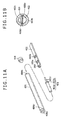
- FIG. 15 shows an example of a schematic structure of a conventional pen type position indicator 100.
- the conventional pen type position indicator 100 of this example shown in FIG. 15 is described in Patent Document 1 of Japanese Patent Laid-Open No. 2002-244806 , and is used for an electromagnetic induction type position detector.
- the conventional pen type position indicator 100 of this example includes a resonance circuit, which has a ferrite core 104 and a ferrite chip 102, and which also has one or more resonance capacitors 115 connected to a coil 105 wound around the ferrite core 104.
- FIG. 15 is a cross sectional view of the position indicator 100, for the sake of clear description, FIG. 15 shows a state in which the coil 105 is wound around the ferrite core 104.
- the conventional pen type position indicator 100 is structured in such a way that the ferrite core 104, around which the coil 105 is wound, and the ferrite chip 102 are made to face each other through an O ring 103, and the ferrite chip 102 comes close to the ferrite core 104 when a pressing pressure (pen pressure) is applied to a core body 101.
- the O ring 103 is a ring-like elastic member which is obtained by forming an elastic material, such as a synthetic resin or a synthetic rubber, into an O-like shape.
- a board holder 113, a board 114, a resonance capacitor 115, a connection line 116 through which the resonance capacitor 115 and the coil 105 are connected to each other, thereby configuring a resonance circuit, a ring type film 117, and a buffer member 118 are accommodated in a hollow chassis (hereinafter simply referred to as "a case") 111, and positions thereof are fixed by a cap 112.
- the components, including the elastic O ring 103, disposed inside the case 111 are directly accommodated in the case 111 in a state in which a biasing force (stress) is directly applied to the case 111.
- the pen type conventional position indicator includes the ferrite core
- the circuit constant is changed, and the change in the inductance due to the adjacency of the ferrite chip 102 deviates from a desired change in some cases.
- the case 111 of the conventional pen type position indicator 100 may be bent into a banana-like shape.
- one approach was adopted to modularize the group of components (e.g., the O ring 103) in a portion, which is elastically biased, and to combine the resulting module with other components, thereby preventing the elastic biasing force described above from being directly applied to the case 111.
- the group of components e.g., the O ring 103
- the present invention is directed to solving the problems described above, and to providing a position indicator which can be formed in a thinner shape while preventing direct application of a stress to a chassis and avoiding the problems as described above.
- the invention is realized by a position indicator according to claim 1.
- Claim 2 to 14 relate to specifically advantageous realizations of the position indicator of claim 1.
- a position indicator including:
- the core body, the one or more pressure-sensitive components, and the printed wired board are disposed and held in the holder, which is accommodated in the inside of the cylindrical chassis.
- the one or more pressure-sensitive components, which are biased by the pressing pressure applied to the core body are disposed in the component disposing portion and held in the holder, the biasing force is not directly applied to the cylindrical chassis.
- the one or more pressure-sensitive components are held such that their central positions are registered with determined positions, respectively, with respect to the holder.
- Each of the central positions of the one or more pressure-sensitive components agrees with a center line position of the core body in the state in which the one or more pressure-sensitive components are held by the holder.
- the position indicator according to the present invention even when a shock is applied to the cylindrical chassis, the center line position of the core body held by the holder, and the center line portions of the one or more pressure-sensitive components also held by the holder can be prevented from being shifted from each other.
- the structure is obtained in which the biasing force due to the internal components is not directly applied to the cylindrical chassis, when adjustments for the core body, the printed wiring board, and the one or more pressure-sensitive components which are all held by the holder are carried out before the holder is accommodated in the cylindrical chassis, it is not necessary to carry out readjustment after the holder is accommodated in the cylindrical chassis.
- the cylindrical chassis even when the position indicator is used for a long period of time or in a severe high-temperature state, the cylindrical chassis is prevented from being deformed into a banana-like shape.
- the one or more pressure-sensitive components which are biased by the pressing pressure applied to the core body, are arranged and disposed in the component disposing portion in the axial line direction with respect to the core body and held by the holder. Therefore, the one or more pressure-sensitive components need not be modularized components and can be arranged as the components suited for thinning the position indicator.
- the holder since the holder only has to be accommodated in the cylindrical chassis after the core body, the one or more pressure-sensitive components, and the printed wiring board are disposed in the holder, ease of manufacturing the position indicator is also improved.
- the core body, the one or more pressure-sensitive components, and the printed wired board are disposed and held in the holder, which is accommodated in the inside of the cylindrical chassis.
- a position indicator capable of preventing (internal) stress from being applied directly to the cylindrical chassis, to improve ease of manufacturing the position indicator, and to make the position indicator thinner.
- Such a position indicator is preferably configured for use with a capacitive type sensor or for use with an electromagnetic induction type sensor.
- the holder is composed of a cylinder body, which is divided into a first accommodation portion and a second accommodation portion along its axial direction; the core body engaging portion, the component disposing portion, and the printed wiring board are included in the first accommodation portion, or are included in both of the first accommodation portion and the second accommodation portion; and the second accommodating portion is engaged with the first accommodating portion to form the cylinder body to enclose therein the core body, the one or more pressure-sensitive components, and the printed wiring board.
- the holder is composed of a cylinder body accommodated in the hollow portion of the cylindrical chassis; the core body, the one or more pressure-sensitive components, and the printed wiring board are inserted into the cylinder body of the holder, in aforementioned order, through an insertion opening provided at an axial end of the cylinder body, and the insertion opening is closed to modularize the holder; and the holder thus modularized is disposed in the hollow portion of the cylindrical chassis.
- FIG. 1 illustrates a structure of a pen-shaped position indicator 1 according to a first embodiment of the present invention.
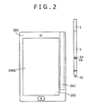
- FIG. 2 is a top plan view showing an example of an electronic apparatus 200 for use with the pen-shaped position indicator 1 according to the first embodiment of the present invention.
- the electronic apparatus 200 is, for example, a high-performance cellular phone unit including a display screen 200D of a display device, such as a Liquid Crystal Display (LCD) device.
- the electronic apparatus 200 includes an electromagnetic induction type position detector 202 on a lower portion (back side) of the display screen 200D.
- a chassis of the electronic apparatus 200 in this case is provided with an accommodation concave hole 201 for accommodating therein the pen-shaped position indicator 1.
- a user takes out the pen-shaped position indicator 1 accommodated in the accommodation concave hole 201 from the electronic apparatus 200 as may be necessary, and carries out a position indicating operation on the display screen 200D of the electronic apparatus 200.
- the position detector 202 provided on the lower portion of the display screen 200D detects both a position, where the operation is carried out by the pen-shaped position indicator 1, and a pen pressure applied to the display screen 200D.
- a microcomputer included in the position detector 202 of the electronic apparatus 200 executes display processing corresponding to both of the operation position and the pen pressure on the display screen 200D.
- FIG. 1 shows an overall structure of the pen-shaped position indicator 1 of the first embodiment.
- FIG. 1 shows the inside of the pen-shaped position indicator 1 by cutting out and removing away a case 2 of the pen-shaped position indicator 1.
- the pen-shaped position indicator 1 includes the case 2, which is long and thin in an axial direction, and which forms a cylindrical chassis having a bottom.
- the case 2 is made of, for example, a resin or the like, and has a cylindrical shape including a hollow portion inside thereof.
- a holder 3 which holds therein a core body 4, a pressure-sensitive component (a component configured to detect a pen pressure) 5, and a printed wiring board 6 is accommodated in the hollow portion of the case 2.
- the holder 3 is made of, for example, a resin.
- the core body 4 is composed of a protrusion member (pen tip member) 41 and a ferrite core 42.
- the pressure-sensitive component 5 is composed of a ferrite chip 51, a coil spring 52, and an elastic body, which is a silicon rubber 53 in this example.
- the ferrite core 42 is an example of a first magnetic body
- the ferrite chip 51 is an example of a second magnetic body.
- One end side in the axial direction of the case 2 is a pen tip side of the pen-shaped position indicator 1, and the pen tip side of the case 2 is provided with a through hole 21, through which the protrusion member (pen tip member) 41 protrudes to the outside.
- the protrusion member 41 On the pen tip side within the case 2 of the pen-shaped position indicator 1, as shown in FIG. 1 , the protrusion member 41 is accommodated in the hollow portion of the case 2 in a state in which a part of the protrusion member 41 protrudes to the outside through the through hole 21.
- the protrusion member 41 includes a guard portion 41a, which engages with the case 2, to be prevented from breaking away from the through hole 21.
- the protrusion member 41 is made of a synthetic resin such as a polyacetal resin (DURACON: registered trademark) to have a sufficient resistance property against friction when the protrusion portion 41 is used in contact with the operation surface.
- the ferrite core 42 as an example of a magnetic material, around which a position indicating coil 43 as an example of an inductance element is wound, is disposed on a side opposite to a protrusion side of the protrusion member 41 within the case 2.
- the ferrite core 42 has a columnar shape.
- the ferrite core 42 forming a part of the core body 4 includes a guard portion 42a whose diameter is larger than that of a winding portion, on which the position indicating coil 43 is wound, on a side opposite to the side of the protrusion member 41.
- the guard portion 42a engages with a core body engaging portion 31 of the holder 3, to be engaged with and held by the holder 3.
- the holder 3 includes a component disposing portion 32, which is formed adjacent to the core body engaging portion 31, and further includes a printed wiring board mounting portion 33 which is formed adjacent to the component disposing portion 32, on a side opposite to the core body 4.
- the ferrite chip 51, the coil spring 52, and the silicon rubber 53, which compose the pressure-sensitive component 5, are arranged in the axial direction along a line extending from the printed wiring board 6 side to the core body 4 side, in order, and are held in the component disposing portion 32.
- a printed wiring board 6 is mounted on the printed wiring board mounting portion 33 of the holder 3.
- a detailed structure of the holder 3, and a structure in which the core body 4, the pressure-sensitive component 5, and the printed wiring board 6 are all held and mounted on the holder 3, will be described in detail later.
- the printed wiring board 6 has a width smaller than an internal diameter of the case 2, and has an elongated rectangular shape. Although an illustration is omitted here for the sake of simplicity, both ends of the position indicating coil 43 are, for example, soldered to a conductive pattern which is formed on the printed wiring board 6.
- the printed wiring board 6 is provided with a push switch 11, which is ON when it is depressed, and turns to an OFF state when it is not depressed.
- the printed wiring board 6 is provided with capacitors 12 and 13 composing, together with the position indicating coil 43, a resonance circuit.
- the capacitor 12 is a trimming capacitor whose capacitance can be adjusted.
- a conductive pattern (not shown) is formed on the printed wiring board 6.
- the capacitor 12 is connected in parallel with the position indicating coil 43
- the capacitor 13 and the push switch 11 are connected in series with each other, and a series circuit of the capacitor 13 and the push switch 11 is connected in parallel with the position indicating coil 43.
- a through hole 14 (refer to FIG. 2 ) is bored in a position, corresponding to the push switch 11, of a peripheral surface of the case 2 of the pen-shaped position indicator 1.
- a pressing operation portion 16 of the push switch 11 is exposed to the outside through the through hole 14 to permit pressing of the push switch 11.
- a predetermined function is allocated by the electronic apparatus 200 including the position detector 202.
- an operation analogous to a clicking operation with a pointing device such as a mouse is allocated to the pressing operation of the push switch 11 via the pressing operation portion 16.
- the capacitors 12 and 13 composing a part of the resonance circuit are disposed as chip components in this case on the printed wiring board 6.
- a resonance frequency of the resonance circuit is adjusted by adjusting the capacitance of the trimming capacitor 12.
- a cover body 17 is mounted so as to be fitted into the case 2, whereby a side of the case 2 opposite to the pen tip side is closed.
- a concave portion 17a is formed approximately in a central portion of a surface of the cover body 17 located in the hollow portion of the case 2.
- a protrusion portion 34a which is fitted into the concave portion 17a, is provided in an end portion 34 of the holder 3 on the cover body 17 side in the axial direction.
- the cover body 17 is mounted to the case 2, whereby the concave portion 17a and the protrusion portion 34a are fitted into each other, and based on this fitting, the holder 3 is engaged within the case 2 in a state in which a center line position of the holder 3 agrees with the center line position of the cylindrical case 2.
- the pressure-sensitive component 5, which is elastically biased in the axial direction of the cylindrical case 2, is held in the component disposing portion 32, and the component disposing portion 32 is provided between the guard portion 42a of the ferrite core 42, which is engaged with the core body engaging portion 31 of the holder 3, and the printed wiring board mounting portion 33 of the holder 3.
- the elastic biasing is generated only within the holder 3. Therefore, a stress due to the elastic biasing of the pressure-sensitive component 5 is prevented from being applied to the case 2.
- FIG. 3 is a block diagram, partly in circuit, showing an example of a circuit configuration of the pen-shaped position indicator 1, and the position detector 202 included in the electronic apparatus 200.
- the pen-shaped position indicator 1 includes the resonance circuit composed of the position indicating coil 43 and the capacitors 12 and 13.
- the resonance circuit is configured in such a way that, as shown in FIG. 3 , the position indicating coil 43 as the inductance element, and the trimming capacitor 12 composed of a chip component, are connected in parallel, and a series circuit of the push switch 11 and the capacitor 13 composed of a chip component is further connected in parallel with the position indicating coil 43 and the trimming capacitor 12.
- the connection of the capacitor 13 to the parallel resonance circuit is controlled in accordance with an ON/OFF operation of the push switch 11, so that the resonance frequency is changed.
- the position detector 202 detects a change in the frequency by detecting a change in the phase of the signal supplied thereto from the pen-shaped position indicator 1, thereby detecting whether or not the push switch 11 has been pressed.
- An X-axis direction loop coil group 211X, and a Y-axis direction loop coil group 212Y are layered on top of each other, thereby forming a position detecting coil in the position detector 202 of the electronic apparatus 200.
- the X-axis direction loop coil group 211X and the Y-axis direction loop coil group 212Y are composed of, for example, n rectangular loop coils and m rectangular loop coils, respectively.
- the loop coils composing the X-axis direction loop coil group 211X and the Y-axis direction loop coil group 212Y, respectively, are disposed in such a way that the loop coils are arranged at an equal interval and are superposed one upon another in order.
- the position detector 202 is provided with a selection circuit 213, to which the X-axis direction loop coil group 211X and the Y-axis direction loop group 212Y are connected.
- the selection circuit 213 successively selects one of the loop coils of the X-axis direction loop coil group 211X, and one of the loop coils of the Y-axis direction loop coil group 212Y.
- the position detector 202 is provided with an oscillator 221, a current driver 222, a switching connection circuit 223, a reception amplifier 224, a detector 225, a low-pass filter 226, a sample-and-hold circuit 227, an analog to digital (A/D) conversion circuit 228, a synchronous detector 229, a low-pass filter 230, a sample-and-hold circuit 231, an A/D conversion circuit 232, and a processing control portion 233.
- the processing control portion 233 is composed of a microcomputer.
- the oscillator 221 generates an alternating-current (AC) signal having a frequency f0.
- the oscillator 221 supplies the AC signal thus generated to each of the current driver 222 and the synchronous detector 229.
- the current driver 222 converts the AC signal supplied thereto from the oscillator 221 into a current, which is in turn supplied from the current driver 222 to the switching connection circuit 223.
- the switching connection circuit 223 switches a connection destination (a transmission side terminal T or a reception side terminal R), to which the loop coil selected by the selection circuit 213 in accordance with the control provided by the processing control portion 233 is connected.
- the current driver 222 is connected to the transmission side terminal T, and the reception amplifier 224 is connected to the reception side terminal R.
- An induced voltage generated in the loop coil selected by the selection circuit 213 is supplied to the reception amplifier 224 through both of the selection circuit 213 and the switching connection circuit 223.
- the reception amplifier 224 amplifies the induced voltage supplied thereto from the loop coil, and supplies the resulting voltage to each of the detector 225 and the synchronous detector 229.
- the detector 225 detects an induced voltage generated in the loop coils, that is, a reception signal, and supplies the detected reception signal to the low-pass filter 226.
- the low-pass filter 226 has a cut-off frequency which is sufficiently lower than the frequency f0 described above, and converts the output signal supplied thereto from the detector 225 into a direct-current (DC) signal, and supplies the DC signal to the sample-and-hold circuit 227.
- the sample-and-hold circuit 227 holds a voltage value at a predetermined timing of the output signal from the low-pass filter 226, specifically, at a predetermined timing during a reception period of time, and supplies the voltage thus held to the A/D conversion circuit 228.
- the A/D conversion circuit 228 converts the analog output supplied thereto from the sample-and-hold circuit 227 into a digital signal and supplies the digital signal to the processing control portion 233.
- the synchronous detector 229 synchronously detects the output signal supplied thereto from the reception amplifier 224 by using the AC signal supplied thereto from the oscillator 221, and supplies a signal set at a level corresponding to a phase difference between the output signal from the reception amplifier 224 and the AC signal from the oscillator 221 to a low-pass filter 230.
- the low-pass filter 230 has a cut-off frequency which is sufficiently lower than the frequency f0 described above, and converts the output signal supplied thereto from the synchronous detector 229 into a DC signal and supplies the DC signal to the sample-and-hold circuit 231.
- the sample-and-hold circuit 231 holds a voltage value at a predetermined timing of the output signal from the low-pass filter 230, and supplies the voltage thus held to the A/D conversion circuit 232.
- the A/D conversion circuit 232 converts the analog output supplied thereto from the sample-and-hold circuit 231 into a digital signal and supplies the digital signal to the processing control portion 233.
- the processing control portion 233 controls operations of the respective portions of the position detector 202. That is to say, the processing control portion 233 controls the operation for selecting the loop coil in the selection circuit 213, the switching operation of the switching correction circuit 223, and the timings of the sample-and-hold circuits 227 and 231.
- the processing control portion 233 transmits the electric wave from the X-axis direction loop group 211 and the Y-axis direction loop group 212 for a given transmission duration time based on input signals supplied thereto from the A/D conversion circuits 228 and 232.
- Induced voltages are generated in the loop coils of the X-axis direction loop group 211 and the Y-axis direction loop group 212 by the electric wave transmitted from the pen-shaped position indicator 1.
- the processing control portion 233 calculates coordinate values of the position in the X-axis direction and the Y-axis direction indicated by the pen-shaped position indicator 1 based on levels of voltage values of the induced voltages generated in the loop coils.
- the processing control portion 233 detects whether or not the push switch 11 has been pressed based on the level of the signal corresponding to the difference in phase between the transmitted electric wave and the received electric wave.
- the processing control portion 233 detects the position indicated by the position indictor 1, which comes close to the position detector 202.
- the position detector 202 detects the phase (frequency biasing) of the received signal, to thereby detect whether or not the pressing operation portion 16 of the pen-shaped position indicator 1 has been depressed.
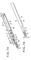
- FIGS. 4A to 4C respectively show a structure of the portions, which are accommodated inside of the case 2 of the pen-shaped position indicator 1. That is to say, FIG. 4B is a perspective view of the holder 3.
- FIG. 4A is an exploded view showing the components held by the holder 3 disposed in the axial direction of the case 2 in the order in which the components are held by the holder 3.
- FIG. 4C is a perspective view showing a state in which the ferrite core 42, the pressure-sensitive component 5, and the printed wiring board 6 are arranged, held, and mounted in the holder 3.
- the components held by the holder 3 are the ferrite core 42 (around which the position indicating coil 43 is wound) of the core body 4, and the entire pressure-sensitive component 5. Also, in this case, the printed wiring board 6 is mounted on the holder 3.
- the pressure-sensitive component 5 is arranged, with the pen tip side set as a base point, by disposing the silicon rubber 53, the coil spring 52, and the ferrite chip 51 in this order in the holder 3. It is noted that in FIG. 4A , as will be described later, a rod-like member 54 disposed adjacent to the ferrite chip 51 is used as an engaging member for engaging the ferrite chip 51 of the pressure-sensitive component 5 with the holder 3 in a state in which the center line position of the ferrite chip 51 agrees with the center line position of the holder 3.
- the holder 3 includes an opening portion (32) that opens in a direction perpendicular to the axial direction of the case 2, which is obtained by partially cutting out the cylinder corresponding to the hollow portion of the case 2 along the axial direction.
- a core body engaging portion 31 is formed in an end portion of the holder 3 corresponding to the side of the core body 4.
- the holder 3 has the opening portion (32) described above adjacent to the core body engaging portion 31.
- the component disposing portion 32 in which the pressure-sensitive component 5 is disposed through the opening portion, is formed in the holder 3.
- the core body engaging portion 31 and the component disposing portion 32 include a peripheral side surface that spans for at least a 180-degree angle range, or more, of the cylinder corresponding to the hollow portion of the case 2.
- An end portion 34 of the holder 3, on the side of the cover body 17, is formed as a circular wall portion to close the cylinder corresponding to the hollow portion of the case 2.
- the printed wiring board mounting portion 33 is formed between the end portion 34 of the holder 3, and the component disposing portion 32.
- the printed wiring board mounting portion 33 includes an elongated mounting flat surface 33a corresponding to the shape of the elongated printed wiring board 6.
- an engaging portion 33b which clamps the elongated printed wiring board 6 on the elongated mounting flat surface 33a by engagement to thereby hold the elongated printed wiring board 6, is formed in the end portion 34.
- a length in a longitudinal direction of the elongated mounting flat surface 33a of the printed wiring board mounting portion 33 is set so as to be approximately equal to or slightly longer than that in the longitudinal direction of the elongated printed wiring board 6.
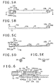
- FIGS. 5A to 5E respectively show an example of a structure of the holder 3.
- FIG. 5A is a top plan view when the holder 3 is viewed from a direction perpendicular to the elongated mounting flat surface 33a of the printed wiring board mounting portion 33.
- FIG. 5B is a side elevational view when the holder 3 is viewed in a direction horizontal with the elongated mounting flat surface 33a of the printed wiring board mounting portion 33.
- FIG. 5C is a cross sectional view taken along line A - A of FIG. 5A.
- FIG. 5D is a view when the holder 3 is viewed in the axial direction from the end portion 34 side of the side elevational view of FIG. 5B .
- FIG. 5E is a cross sectional view taken along line B - B of FIG. 5C .
- FIG. 6 is a partial view showing a state in which the ferrite core 42 and the pressure-sensitive component 5 are accommodated and held in the core body holding portion 31 and the component disposing portion 32 of the holder 3, respectively.
- the holder 3 is shown in the state of the cross sectional view of FIG. 5C .
- an inner diameter of the core body engaging portion 31 is selected as being slightly larger than a diameter of the portion of the ferrite core 42, around which the position indicating coil 43 is wound.
- a coupling portion of the component disposing portion 32 with the core body engaging portion 31 is structured so as to have a slightly larger inner diameter than an outer diameter of the guard portion 42a of the ferrite core 42.
- a stepped portion 31a is formed in the coupling portion between the core body engaging portion 31 and the component disposing portion 32.
- the ferrite core 42 engages with the core body engaging portion 31 such that its guard portion 42a is disposed on the component disposing portion 32 side with respect to the core body engaging portion 31.
- the presence of the stepped portion 31a prevents the ferrite core 42 from falling out of the holder 3 in the axial direction toward the pen tip side.
- the component disposing portion 32 has an opening through which to receive the guard portion 42a of the ferrite core 42, and the core body engaging portion 31 also holds the guard portion 42a of the ferrite core 42 for at least a 180-degree angle range, or more.
- the ferrite core 42 is held such that its center line position aligns with the center line position of a virtual cylinder within the holder 3, in a manner not to fall out of the core body engaging portion 31 in a direction perpendicular to the axial direction.
- the silicon rubber 53 of the pressure-sensitive component 5, as shown in FIG. 4A includes a protrusion portion 53a.
- the end surface of the guard portion 42a of the ferrite core 42 is provided with a concave hole 42b, into which the protrusion portion 53a of the silicon rubber 53 is fitted.
- the protrusion portion 53a of the silicon rubber 53 is press-fitted into the concave hole 42b of the guard portion 42a of the ferrite core 42, whereby the silicon rubber 53 is mounted to the end surface of guard portion 42a of the ferrite core 42.
- An outer diameter of the silicon rubber 53 is selected as smaller than a diameter of the end surface of the guard portion 42a of the ferrite core 42.
- the pressure-sensitive component 5 is held by the coil spring 52 in a state such that the end surface of the ferrite chip 51 defines a predetermined air gap Ar with respect to the silicon rubber 53 mounted to the end surface of guard portion 42a of the ferrite core 42, as shown in FIG. 6 .
- the component disposing portion 32 includes a wall portion 32a, which abuts against the end surface of the guard portion 51a of the ferrite chip 51 so as to prevent the component disposing portion 32 from being moved to the end surface 34 side in the axial direction.
- a through hole 32f through which the rod-like member 54 is inserted is formed in the wall portion 32a in the central position of a virtual cylindrical shape of the holder 3.
- a fitting concave portion 32b for a distance from the wall portion 32a toward the core body engaging portion 31 side corresponding to the thickness of the guard portion 51a of the ferrite chip 51, a fitting concave portion 32b, whose inner diameter is equal to or slightly larger than the outer diameter of the guard portion 51a, is formed.
- a stepped portion 32c On the core body engaging portion 31 side adjacent to the fitting concave portion 32b, a stepped portion 32c, whose inner diameter is equal to or slightly larger than an outer diameter of a small diameter portion of the ferrite chip 51 excluding the guard portion thereof, is formed. Further, on the core body engaging portion 31 side adjacent to the stepped portion 32c, a coil disposing portion 32d is formed, whose inner diameter is equal to the diameter used to form the stepped portion 31a, which is slightly larger than the guard portion 42a of the ferrite core 42.
- a length in the axial direction of the coil disposing portion 32d extends from the position of the stepped portion 31a for the core body engaging portion 31 to the position of the stepped portion 32e formed between the coil disposing portion 32d and the stepped portion 32c. Also, the length in the axial direction of the coil disposing portion 32d is set such that the pressure-sensitive component 5 can be held in a state in which the end surface of the ferrite chip 51 on the side opposite to the guard portion 51a defines the predetermined air gap Ar in the axial direction with respect to the silicon rubber 53 mounted to the end surface of the guard portion 42a of the ferrite core 42.
- the ferrite core 42 to which the silicon rubber 53 is mounted via the end surface of the guard portion 42a, is disposed on the side of the core engaging portion 31 of the coil disposing portion 32d.
- the guard portion 51a of the ferrite chip 51 is fitted into the fitting concave portion 32b of the component disposing portion 32, in a state in which the guard portion 51a of the ferrite chip 51 abuts against the wall portion 32a.
- the guard portion 51a cannot be moved in the axial direction due to the provision of a stepped portion formed between the fitting concave portion 32b and the stepped portion 32c.
- the coil spring 52 has a larger winding diameter than the outer diameter of the silicon rubber 53. For this reason, as shown in FIGS. 1 and 6 , one end side of the coil spring 52 in the elastic biasing direction abuts against the end surface of the guard portion 42a of the ferrite core 42 in a state in which the silicon rubber 53 is accommodated within the size of the winding diameter of the coil spring 52. On the other hand, the other end side of the coil spring 52 in the elastic biasing direction abuts against the stepped portion 32e formed between the stepped portion 32c and the coil disposing portion 32d. By operation of the coil spring 52, the ferrite core 42 is elastically biased toward the pen tip side, constantly, to be engagingly held in the core body engaging portion 31.
- a worker first fits and mounts the silicon rubber 53 to the ferrite core 42. Thereafter, the worker mounts the coil spring 52 to the small diameter portion of the ferrite chip 51, and temporarily couples the silicon rubber 53 mounted to the ferrite core 42 with the end surface of the ferrite chip 51 while inserting the silicon rubber 53 into the size of the winding diameter of the coil spring 52. In this state, the worker inserts the silicon rubber 53 mounted to the ferrite core 42 into the component disposing portion 32 of the holder 3 through its opening portion.
- the silicon rubber 53 is inserted into the size of the winding diameter of the coil spring 52 in such a way that the guard portion 51b of the ferrite chip 51 is fitted into the fitting concave portion 32b, and the coil spring 52 abuts against both of the end surface of the guard portion 42a of the ferrite core 42, and the stepped portion 32e formed between the stepped portion 32c and the coil disposing portion 32d.
- the ferrite core 42 is elastically biased to the core body engaging portion 31 side constantly.
- the ferrite core 42 is held in a state in which the air gap Ar is defined between the silicon rubber 53 and the end portion of the small diameter portion of the ferrite chip 51.
- the concave hole 51b is formed in the central portion of the end surface of the guard portion 51a of the ferrite chip 51, and the rod-like member 54 is fitted into the concave hole 51b through the through hole 32f of the wall portion 32a.
- the ferrite chip 51 is held in such a way that the center line position thereof agrees with the center line position of the virtual cylinder of the holder 3.
- the ferrite core 42 is held by the core body engaging portion 31 in such a way that the center line position thereof agrees with the center line position of the virtual cylinder of the holder 3. Therefore, all of the center line positions of the components disposed in the component disposing portion 32 agree with the center line position of the virtual cylinder of the holder 3.
- the printed wiring board 6 is mooted on the mounting flat surface 33a of the printed wiring board mounting portion 33 of the holder 3. An end edge of the printed wiring board 6 on the end portion 34 side is clamped and engaged by the engaging portion 33b provided in the end portion 34 of the holder 3, and another end edge of the printed wiring board 6 on the component disposing portion 32 side is clamped by the rod-like member 54.
- both of the ferrite core 42, around which the position indicating coil 43 is wound, and the pressure-sensitive component 5 is held by the holder 3. Also, in the state in which the printed wiring board 6 is mounted on and engaged with the holder 3, the protrusion member (the pen tip member) 41 of the core body 4 is further mounted to the tip of the ferrite core 42. In addition, the holder 3 is inserted into the hollow portion of the case 2. Finally, the case 2 is closed by the cover body 17.
- the protrusion portion 34a formed in the end portion 34 of the holder 3 is fitted into the concave portion 17a of the cover body 17, and the holder 3 is engaged within the case 2 in a state in which the center line position of the holder 3 agrees with the center line position of the case 2 having a cylindrical shape.
- the end surface of the ferrite chip 51 is brought into contact with the silicon rubber 53 to elastically bias the silicon rubber 53.
- the inductance of the position indicating coil 43 is changed in accordance with the change characteristics corresponding to the modulus of elasticity of the silicon rubber 53, and thus the phase (resonance frequency) of the electric wave transmitted from the position indicating coil 43 of the resonance circuit is changed.
- the modulus of elasticity of the coil spring 52 is made smaller than that of the silicon rubber 53. That is to say, when k1 is the modulus of elasticity of the coil spring 52, and k2 is the modulus of elasticity of the silicon rubber 53, a relationship of k1 ⁇ k2 holds. Therefore, the coil spring 52 is elastically deformed by a smaller pressing pressure than that for the silicon rubber 53. Thus, the silicon rubber 53 is not elastically deformed unless the pressing pressure larger than that for the coil spring 52 is applied.
- both of the coil spring 52 and the silicon rubber 53 are interposed between the ferrite core 42 and the ferrite chip 51.
- the ferrite core 42 is pulled away from the ferrite chip 51 by mainly the operation of the coil spring 52, even when the pen tip side of the pen-shaped position indicator 1 is pointed upward, the ferrite core 42 and the ferrite chip 51 are prevented from coming close to each other. Therefore, even when the pen-shaped position indicator 1 is handled in such a way that the protrusion member 41 is directed upward, erroneous detection of a pressing pressure is prevented.
- the coil spring 52 and the silicon rubber 53 it is possible to widen the detection range of the pressing pressure (pen pressure) applied to the core body 4 composed of the protrusion member 41 and the ferrite core 42. Furthermore, the electric wave whose phase (frequency) is suitably changed in correspondence to the pressing pressure can be transmitted to the position detector 202 and thus the detection of the pressing pressure (pen pressure) can be properly carried out.
- the pen-shaped position indicator 1 of the first embodiment described above is structured in such a way that all of the components accommodated in the case 2 are held by the holder 3, and the pressure-sensitive component 5 undergoes the elastic biasing force in the component disposing portion 32 of the holder 3, the elastic biasing force is prevented from being applied to the case 2. For this reason, even when the components are accommodated in the holder 3 and adjusted, and the holder 3 is then accommodated in the case 2, it is not necessary to carry out readjustment of the components. In addition, even when the pen-shaped position indicator 1 is placed in a severe condition such as a long usage or a high-temperature state, the case 2 can be prevented from being deformed into a banana-like shape.
- the components are merely disposed side by side in the holder 3 along the axial direction, whereby the components can be held in the holder 3 in the state in which the center line position of the case 2 is aligned with each of the center line positions of the components. Also, in that state, the components can be handled as if the components are modularized. Therefore, work efficiency in manufacture of the present indicator 1 is improved.
- the pressure-sensitive component is not formed in the form of a modularized component, but is merely disposed in the holder 3. Therefore, a thin type of the pen-shaped position indicator 1 can be achieved by simply miniaturizing respective components.
- the individual components are inserted from the opening portions corresponding to the outer diameters of the individual components, respectively.
- the holder 3 is made of a material, such as a resin having elasticity
- the opening portions whose sizes are smaller than the outer diameters of the individual components, respectively may be provided.
- insertion of the individual components can be carried out by elastically biasing the holder 3, and after completion of the insertion of the individual components, the return of the elasticity serves to prevent the individual components from deviating from their respective positions in the axial direction.
- the holder 3 has the shape which is obtained by partially cutting out the cylinder corresponding to the hollow portion of the case 2 along the axial direction, and the cut-out portion is held as the opening portion.
- a second embodiment of the present invention is a modification of the first embodiment of the present invention to address this problem.
- the same constituent elements as those in the first embodiment of the present invention are designated by the same reference numerals or symbols, respectively, and a description thereof is omitted here for the sake of simplicity.
- the cylinder corresponding to the hollow portion of the case 2 is divided into two parts along the axial direction, and thus the holder 30 in this embodiment is composed of a first holder 3A as a first accommodating portion, and a second holder 3B as a second accommodating portion.
- the first holder 3A and the second holder 3B are coupled to each other by a hinge provided along the axial direction.
- the first holder 3A and the second holder 3B may be arranged separately from each other.
- the first holder 3A has substantially the same structure as that of the holder 3 described above, and the core body engaging portion 31, the component disposing portion 32, and the printed wiring board mounting portion 33 are formed in the first holder 3A.
- the second holder 3B is formed in the form of a portion corresponding to a portion which is obtained by removing the first holder 3A from the cylinder corresponding to the hollow portion of the case 2.
- the ferrite core 42 and the pressure-sensitive component 5 are respectively disposed on the core body engaging portion 31 and the component disposing portion 32 of the first holder 3A, and the printed wiring board 6 is mounted on the printed wiring board mounting portion 33 of the first holder 3A, in the manner as described in the first embodiment described above. Thereafter, the opening portion of the first holder 3A is covered with the second holder 3B to be closed, thereby forming the cylinder corresponding to the hollow portion of the case 2, as shown in FIG. 7B . Note that, in the state of the cylinder, it is better that the first holder portion 3A and the second holder portion 3B are jointed to each other by an adhesive material or bonded to each other by an adhesive tape.
- the cylindrical holder 30 is structured in a cylindrical shape, which can be used as an independent component.
- all of the core body engaging portion, the component disposing portion, and the printed wiring board mounting portion are formed in only one of the first accommodating portion (first holder portion) and the second accommodating portion (second holder portion).
- a structure may also be adopted such that the core body engaging portion, the component disposing portion, and the printed wiring board mounting portion are dividedly provided in the first accommodating portion and the second accommodating portion, as may be necessary in such a way that, for example, the printed wiring board mounting portion is provided in the second accommodating portion while the others are provided in the first accommodating portion.
- the pressure-sensitive component in the position indicator according to each of the first and second embodiments of the present invention is of the type in which the change in the inductance is detected
- the pressure-sensitive component may also be of the type in which the pressing pressure (pen pressure) applied to the core body is detected based on the change in a capacitance.
- the pressure-sensitive component is of a type in which the pressing pressure is detected by detecting the change in a capacitance.
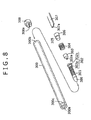
- FIG. 8 is a view showing a holder 300 and internal components thereof in a position indicator according to the third embodiment of the present invention.
- FIG. 9 is a view illustrating a state in which the internal components are accommodated in the holder 300.
- the holder 300 has a hollow-cylindrical shape.
- the holder 300 is also made of a resin, for example.
- an inner diameter of an opening portion 300a of the holder 300 on the pen tip side is set as a diameter R1 corresponding to a diameter of a small diameter portion 302a of a ferrite core 302, around which a position indicating coil 301 is wound.
- An inner diameter of an opening portion 300b of the holder 300 on the side opposite the pen tip side is set as a radius R2 (R2 > R1) corresponding to an outer diameter of a guard portion 302b of the ferrite core 302.
- an inner diameter of a portion extending for a short distance from the opening portion 300a on the pen tip side is set as the diameter R1
- an inner diameter of the rest of the holder 300 is set as the radius R2 which is equal to that of the opening portion 300b.
- a stepped portion 300c is formed between the portion extending for a short distance from the opening portion 300a and the rest of the holder 300.
- the pressure-sensitive component is composed of an electric conductor 303 forming one electrode of a capacitor, a coil spring 304, a dielectric body 305, and an electric conductor 306 forming the other electrode of the capacitor.
- the electric conductor 303 is composed of a conductive elastic body which can be elastically biased.
- the electric conductor 303 and the electric conductor 306 face each other through the dielectric body 305.
- a surface of the electric conductor 303 facing the dielectric body 305 has a dome-like shape which bulges toward the dielectric body 305 side.
- These components composing the pressure-sensitive component are inserted into the holder 300 in the order shown in the figure.
- the side of the opening portion 300b of the holder 300 is closed, for example, by a cover body 308 which, for example, accommodates therein a printed wiring board 307 in a groove 308a which extends through a center of the cover body 308.
- the following procedure can be adopted. Firstly, the worker arranges the components on a tray for insertion, in the order of the insertion of the components into the holder 300. After that, a pressing operation machine pushes the components arranged on the tray for insertion, so that the components are automatically inserted into the hollow portion of the holder 300 in order.
- a guard portion 302b of the ferrite core 302 is engaged with the stepped portion 300c within the hollow portion of the holder 300, whereby the ferrite core 302 is engaged within the hollow portion of the holder 300.
- a concave hole 302c is provided in the end surface of the guard portion 302b of the ferrite core 302.
- the electric conductor 303 includes a protrusion portion 303a which is fitted into the concave hole 302c.
- the protrusion portion 303a is fitted into the concave hole 302c, whereby the electric conductor 303 is mounted to the end surface of the guard portion 302b of the ferrite core 302.
- a diameter of the electric conductor 303 is made identical to that of the dielectric body 305.
- the electric conductor 303 and the dielectric body 305 are disposed in such a way that the end surfaces of the electric conductor 303 and the dielectric body 305 face each other through an air gap Ar1 created by operation of the coil spring 304.
- a winding diameter of the coil spring 304 is made larger than each of the diameters of the electric conductor 303 and the dielectric body 305. Also, one end side of the coil spring 304 in the axial direction abuts against the end surface of the guard portion 302b of the ferrite core 302, and the other end side thereof abuts against the end surface of the electric conductor 306, into which the dielectric body 305 is fitted in a state in which both of the electric conductor 303 and the dielectric body 305 are accommodated in the wiring frame of the coil spring 304.
- a diameter of the electric conductor 306, as shown in FIG. 9 is set as the radius R2.
- a concave portion 306a is formed in the end surface of the electric conductor 306 on the side opposite from a coupling portion with the dielectric body 305.
- a protrusion portion 307a which is adapted to be fitted into the concave portion 306a, is formed in the end portion of the printed wiring board 307. Therefore, a position of the end portion of the printed wiring board 307 on the electric conductor 306 side is fixed based on the protrusion portion 307a being fitted into the concave portion 306a of the electric conductor 306, and the printed wiring board 307 is held in the holder 300.
- the electric conductor 303 and the electric conductor 306 are spaced away from each other by operation of the coil spring 304, and are held so as to face each other through both of the air gap Arl and the dielectric body 305.
- the electric conductor 303 and the electric conductor 306 are electrically connected to each other so as to be connected in parallel with the ferrite coil 301 in the printed wiring board 307.
- the end surface of the electric conductor 303 when the pressing pressure is applied from the side of the protrusion member 309 forming the pen tip to the electric conductor 303 through the ferrite core 302, the end surface of the electric conductor 303, which bulges in the dome-like shape, is biased against the biasing force of the coil spring 304 to come close to and contact the end surface of the dielectric body 305.
- the capacitor is connected in parallel with the position indicating coil 301 to form the resonance circuit, the resonance frequency of the resonance circuit is changed so as to correspond to the capacity thus changed. That is to say, the phase (resonance frequency) of the electric wave transmitted from the position indicating coil 301 of the resonance circuit is changed accordingly.
- the pressure-sensitive component is subjected to the elastic biasing force within the holder 300.
- the elastic biasing force is prevented from being applied as a stress to the case 2.
- all of the components are inserted into and held in the holder 300 having a cylindrical shape in such a way that the center line positions of all of the components agree with one another within the holder 300.
- the position indicator according to the third embodiment of the present invention also offers the same effects as those of each of the position indicators according to the first and second embodiments of the present invention, and thus can be readily made thin.
- the position indicating coil 301 which is wound around the small diameter portion 302a of the ferrite core 302, protrudes from the opening portion 300a of the holder 300.
- another structure may be adopted such that the position indicating coil 301 is accommodated in the holder 300 in such a way that only a protrusion member coupled to the ferrite core 302 protrudes from the opening portion 300a of the holder 300 to the outside.
- FIG. 10 is a view showing an arrangement of the components within the holder 300 in such a case.
- the protrusion member 310 which is fitted into the side opposite to the guard portion 302b of the ferrite core 302, has a shape including both of a guard portion 310b and a small diameter portion 310a.
- a diameter of the small diameter portion 310a of the protrusion member 310 is set slightly smaller than the inner diameter R1 of the opening portion 300a of the holder 300.
- an outer diameter of the guard portion 310b of the protrusion member 310 is set between the inner diameter R1 of the opening portion 300a of the holder 300 and the inner diameter R2 of the opening portion 300b.
- the case 2 of the position indicator includes a stepped portion provided in the opening portion on the pen tip side.
- the end surface of the opening portion 300a of the holder 300 is engaged with the stepped portion of the case 2 to be locked.
- the case 2 is covered with a cover body 17 (see FIG. 1 ), whereby the holder 300 is regulated so as not to move in the axial direction of the case 2.
- the holder 300 in which the individual components are accommodated and held can be used as a replacement lead for the case of the position indicator.
- a pressure-sensitive component is of a type in which a pressing pressure is detected based on a change in capacitance.
- the pressure-sensitive component is composed of a semiconductor device called Micro Electro Mechanical System (MEMS).
- MEMS Micro Electro Mechanical System
- the pressure-sensitive component is composed of a single capacitance type pressure sensing semiconductor device (hereinafter referred to as "a pressure sensing device").
- each of the position indicators of the first to third embodiments has the structure as a position indicator for an electromagnetic induction type position detector
- the present invention can be applied in a position detector for a capacitance type position detector.
- the fourth embodiment of the present invention is directed to a position detector for the capacitance type position detector.
- FIGS. 11A and 11B respectively show a holder 400, and internal components accommodated in the holder 400 in a position indicator according to the fourth embodiment of the present invention.
- the holder 400 is made of a resin, for example, and has a hollow cylindrical shape similarly to the case of the third embodiment of the present invention.
- an inner diameter of an opening portion 400a serving as a pen tip side is set as a diameter R11 corresponding to a diameter of a small diameter portion 401a of a core body 401 formed of an electric conductor.
- An inner diameter of an opening portion 400b of the holder 400 on a side opposite to the pen tip side is set as a diameter R12 (R12 > R11) corresponding to an outer diameter of a guard portion 401b of the core body 401.
- a protrusion member (not shown) composed of an electric conductor is coupled to the core body 401.
- the core body 401 is electrically connected to a case composed of an electric conductor such as a conductive metal.
- an inner diameter of a portion extending for a short distance from an opening portion 400a on the pen tip side is set as a diameter R11
- an inner diameter of the rest of the holder 400 is set as a diameter R12, which is identical to that of the opening portion 400b.
- a stepped portion 400c is formed between the portion extending for a short distance from the opening portion 400a and the rest of the holder 400.
- a depressing member 401c for depressing a pressure sensing device 500 is formed in the core body 401.
- the pressure sensing device 500 is provided on an end surface of a printed wiring board 402.
- a width of the printed wiring board 402 is set slightly wider than the inner diameter R12 of the holder 400.
- grooves 400d and 400e are formed in an inner wall surface of the holder 400 to extend along the axial direction. Thus, both side edges in a longitudinal direction of the printed wiring board 402 are inserted into and held in the groves 400d and 400e, respectively.
- the small diameter portion 401a of the core body 401 protrudes from the opening portion 400a to the outside.
- the guard portion 401b of the core body 401 is engaged with the stepped portion 400c provided within the hollow portion of the holder 400, whereby the core body 401 is associated within the holder 400.
- a cover body 410 is fitted into the holder 400 so as to close the opening portion 400b side of the holder 400, whereby the depressing member 401c provided in the core body 401 abuts against the pressure sensing device 500 provided on the end surface of the printed wiring board 402.
- the printed wiring board 402 is provided with a circuit element 403a to detect a variable capacitance of the pressure sensing device 500 as, for example, a frequency change, and a circuit element 403b to transmit information on a pen pressure corresponding to the variable capacitance thus detected wirelessly by infrared wave, radio wave, or the like.
- the holder 400 in which both of the core body 401 and the printed wiring board 402 are accommodated and held, is accommodated in a case of the position indicator.
- the pressure sensing device 500 When the depressing force is received in the position indicator through the protrusion member as the pen tip member mounted to the tip of the core body 401, the pressure sensing device 500 is depressed by the depressing force, so that the capacitance of the pressure sensing device 500 is changed.
- the circuit element 403a detects the capacitance thus changed, and the circuit element 403b supplies the information on the pen pressure corresponding to the capacitance detected by the circuit element 403a to the capacitance type position detector, wirelessly.
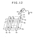
- FIG. 12 An example of the capacitance type position detector used in the position indicator of the fourth embodiment is shown in FIG. 12 .
- a sensor portion of the capacitance type position detector in this example is structured in such a way that plural upper electrodes Ex extending in a Y-axis direction (in a vertical direction), for example, and plural lower electrodes Ey extending in an X-axis direction (in a horizontal direction), for example, are arranged on an indication input surface in the X-axis direction and in the Y-axis direction at predetermined intervals, respectively.
- the upper electrodes Ex and the lower electrodes Ey intersect each other perpendicularly and are laid out with a slight gap in between.
- a capacitor (fixed capacitor) having a predetermined capacitance Co is formed at each cross-point between the upper electrode Ex and the lower electrode Ey.
- a capacitor having a capacitance Cf is formed between the electrodes Ex and Ey at this position and the indication body.
- the indication body such as the position indicator 1A is connected to the ground through the human body and a predetermined capacitor having a capacitance Cg.
- the position which is indicated by the indication body such as the position indicator 1A within the indication input surface is specified by detecting the change in the amount of movement of the electric charge accumulated between the upper electrode Ex and the lower electrode Ey.
- the lower electrode Ey is used as a transmission electrode and a predetermined signal is transmitted to the transmission electrode; and the upper electrode Ex is used as a reception electrode and a current change in the received signal from the reception electrode is detected, thereby detecting the change in the amount of movement of the electric charge.
- the position detector also includes a circuit for receiving information on a pen pressure transmitted from the position indicator wirelessly to thereby detect the pen pressure.
- FIGS. 13A to 13C respectively show a structure of the pressure sensing device in this example. That is to say, FIG. 13A is a perspective view of the pressure sensing device in this example. FIG. 13B is a longitudinal cross sectional view taken along line C - C of FIG. 13A. FIG. 13C is a partial perspective view of the pressure sensing device 500 which, in this example, is mounted to the printed wiring board 402.
- the pressure sensing device 500 in this example is manufactured in such a way that a pressure-sensitive chip 600 structured as a semiconductor device manufactured by utilizing the MEMS technique, for example, is encapsulated in a cube or a rectangular parallelepiped-like box type package 510 (see FIGS. 13A and 13B ).
- the pressure-sensitive chip 600 serves to detect a pressure applied thereto in the form of a change in capacitance.
- the pressure-sensitive chip 600 has a structure as shown in FIGS. 13A to 13C .
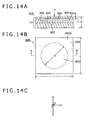
- FIG. 14B is a top plan view of the pressure-sensitive chip 600 in this example when viewed from a surface 601 a side, which receives a pressure P.
- FIG. 14A is a longitudinal cross sectional view taken along line D - D of FIG. 14B .
- L 1.5 mm
- H 0.5 mm.
- the pressure-sensitive chip 600 in this example is composed of a first electrode 601, a second electrode 602, and an insulating layer (dielectric layer) 603 between the first electrode 601 and the second electrode 602.
- each of the first electrode 601 and the second electrode 602 is composed of an electric conductor made of single crystal silicon (Si).
- the insulating layer 603, in this example, is made of a silicon oxide (SiO 2 ) film. It is noted that the insulating layer 603 needs not to be made of the oxide film, but may be made of any other suitable insulator.
- a concave portion 604 having circular shape with a central position of the surface as a center is formed on a surface of the insulating layer 603 facing the first electrode 601. Due to the presence of the concave portion 604, a space 605 is defined between the insulating layer 603 and the first electrode 601.
- a bottom surface of the concave portion 604 is formed as a flat surface, and a radius R of the bottom surface of the circular concave portion 604 is set to 1 mm, for example.
- a depth of the concave portion 604 is set to the range of about several tens of micrometers to about a hundred micrometers.
- the pressure-sensitive chip 600 in this example is made in a semiconductor process in the manner as will be described below. Firstly, the insulating layer 603 composed of the oxide film is formed on single crystal silicon forming the second electrode 602. Next, an annular mask having a radius R is formed on the insulating layer 603 composed of the oxide film, and etching is carried out with respect to the insulating layer 603, thereby forming the concave portion 604. Then, single crystal silicon composing the first electrode 601 is deposited on the insulating layer 603. As a result, the pressure-sensitive chip 600 is formed, which includes the space 605 under the first electrode 601.
- a thickness t of single crystal silicon as a sample material for forming the first electrode 601 is set as a thickness that permits the first electrode 601 to be bent by the pressure P applied to the pressure-sensitive chip 600.
- the first electrode 601 is set as being thinner than the second electrode 602.
- the thickness t of the first electrode 601 is selected in such a way to achieve desirable bending displacement characteristics of the first electrode 601 in response to the applied pressure P.
- a capacitor having a capacitance Cv is formed between the first electrode 601 and the second electrode 602. Also, as shown in FIG. 14A , when the pressure P is applied to the first electrode 601 from the side of an upper surface 601 a of the first electrode 601 opposite to the surface facing the second electrode 602, the first electrode 601 is bent as indicated by a dotted line in FIG. 14A , and thus a distance between the first electrode 601 and the second electrode 602 becomes short, so that the value of the capacitance Cv is changed to become large. An amount of bending of the first electrode 601 is changed in accordance with the magnitude of the applied pressure P. Therefore, as shown in an equivalent circuit of FIG. 14C , the capacitance Cv becomes a variable capacitance, which is changed in accordance with the magnitude of the pressure P applied to the pressure-sensitive chip 600.
- the pressure-sensitive chip 600 having the structure as described above is accommodated in a package 510 in a state in which the surface 601a of the first electrode 601 which receives the pressure applied thereto, as shown in FIGS. 13A and 13B , is parallel with the upper surface 510a of the package 510, and faces the upper surface 510a of the package 510.
- the package 510 is composed of a package member 511 made of an electric insulating material such as a ceramic material or a resin material, and an elastic member 512 which is provided on the side of the surface 601a of the pressure-sensitive chip 600, which receives the pressure in the package member 511.
- the elastic member 512 is an example of a pressure transferring member.
- a concave portion 511a is provided above the pressure-receiving surface 601a of the first electrode 601 of the pressure-sensitive chip 600 encapsulated within the package member 511.
- the concave portion 511a covers an area of the pressure-receiving portion of the pressure-sensitive chip 600.
- the elastic member 512 is filled in the concave portion 511a. That is to say, the elastic member 512 is arranged within the concave portion 511a of the package member 511 so as to be integrated with the package 510.
- the elastic member 512 is made of a silicon resin, especially, made of a silicon rubber.
- a communication hole 513 which communicates from the upper surface 510a of the package 510 to a portion of the elastic member 512, is formed in the package 510. That is to say, a through hole 511b constituting a portion of the communication hole 513 is formed in the package member 511. Also, a concave hole 512a constituting a tip portion of the communication hole 513 is provided in the elastic member 512. In addition, a tapered portion 511c is formed on an opening portion side (on the upper surface 510a side) of the communication hole 513 of the package member 511, and the opening portion of the communication hole 513 has a funnel-like shape.
- the depressing member 401c provided in the core body 401 is inserted into the pressure sensing device 500 through the communication hole 513.
- the pressure P applied from the outside is applied in the axial direction (in the center line direction) of the depressing member 401c.
- a diameter of the through hole 511b is set as being slightly larger than that of the depressing member 401c
- a diameter of the concave hole 512a is set as being slightly smaller than that of the depressing member 401c.
- the depressing member 401c Since the opening portion of the communication hole 513 has the funnel-like shape, the depressing member 401c is guided by the tapered portion 511c of the opening portion of the communication hole 513, and is readily introduced and inserted into the communication hole 513. Also, the depressing member 401c is pushed into the inside of the concave hole 512a of the elastic member 512 at the end portion of the communication hole 513. In such a manner, the depressing member 401c is inserted into the communication hole 513 of the pressure sensing device 500, to be thereby positioned to apply the pressure P in the axial direction to the pressure-receiving surface side of the pressure-sensitive chip 600.
- the depressing member 401c is elastically held in the concave hole 512a of the elastic member 512 by the elastic member 512.
- the depressing member 401c is held by the pressure sensing device 500.
- the depressing member 401c is drawn out from the communication hole 513 by using a predetermined force, thereby making it possible to release the holding state by the pressure sensing device 500.
- a first lead terminal 521 connected to the first electrode 601 of the pressure-sensitive chip 600 is derived from the package member 511 of the pressure sensing device 500, and a second lead terminal 522 connected to the second electrode 602 of the pressure-sensitive chip 600 is also derived from the package member 511 of the pressure sensing device 500.
- the first lead terminal 521 is electrically connected to the first electrode 601 by, for example, a gold wire 523.
- the second lead terminal 522 is derived from the package member 511 of the pressure sensing device 500 in a state in which the second lead terminal 522 contacts the second electrode 602, thereby being electrically connected to the second electrode 602.
- the second lead terminal 522 and the second electrode 602 may be electrically connected to each other by a gold wire or the like.
- each of the first and second lead terminals 521 and 522 is made of a conductive metal, and as shown in FIG. 13A , is formed to have a large width.
- the first and second lead terminals 521 and 522 are derived from a bottom surface 510b parallel with the upper surface 510a of the package 510 in a direction perpendicular to the bottom surface 510b, and are also derived so as to face each other at an interval corresponding to a thickness d of the printed wiring board 402.
- the pressure sensing device 500 is disposed in such a way that a thickness direction of the printed wiring board 402 is clamped between the first and second lead terminals 521 and 522 in a state in which the bottom surface 510b of the package 510 is brought into contact with the end surface 402a of the printed wiring board 402.
- a printed pattern 701 provided on a first surface 402b of the printed wiring board 402, and the first lead terminal 521, are fixed to each other by soldering.
- a printed pattern provided on a second surface of the printed wiring board 402 opposite to the first surface 402b, and the second lead terminal 522, are fixed to each other by soldering.
- a signal processing circuit for example, composed of an IC
- the printed pattern to which the second lead terminal 522 is soldered is provided on the second surface of the printed wiring board 402 opposite to the first surface 402b, the printed pattern is connected to the printed pattern on the side of the first surface 402b via a through hole of the printed wiring board 402 to be connected to the signal processing circuit.
- the pressure-receiving surface 601a of the pressure-sensitive chip 600 on the side of the pressure-receiving surface 601a of the pressure-sensitive chip 600, the pressure is applied to the entire surface 610a by the elastic member 512.
- the pressure corresponding to the pressing pressure P is efficiently applied to the pressure-sensitive chip 600, and the pressure-sensitive chip 600 desirably exhibits the capacitance Cv corresponding to the pressing pressure P.
- the elastic member 512 is interposed between the depressing member 401c and the pressure-sensitive chip 600, a pressure resistance property of the pressure-receiving surface side of the pressure-sensitive chip 600 is enhanced, and thus the surface side can be prevented from being damaged by the pressure. That is to say, since in the pressure sensing device 500, the pressure based on the pressing pressure P applied from the outside is received by the pressure-sensitive chip 600 through the elastic member 512 serving as a pressure transmitting member, it is possible to increase the pressure resistance property of the pressure-sensitive chip 600 against the applied pressure.
- the depressing member 401c is inserted into the communication hole 513 provided in the package 510 of the pressure sensing device 500 to be precisely positioned, and thus the pressure applied by the depressing member 401c is reliably applied to the pressure-sensitive chip 600 through the elastic member 512.
- the pressing pressure applied through the pressing member 401c is transferred in the form of a pressure, which is applied to the entire surface 601a of the first electrode 601 of the pressure-sensitive chip 600, by the elastic member 512. Therefore, the pressing pressure applied through the depressing member 401c is efficiently applied to the pressure-receiving surface 601a of the pressure-sensitive chip 600, and thus the value of the capacitance Cv of the capacitor of the pressure-sensitive tip 600 exhibits a change which quickly responds to the pressing pressure P.
- the pressure sensing device 500 in the fourth embodiment exhibits a change in the capacitance which quickly responds to the pressing pressure P, and when the pressure sensing device 500 is used for detection of the pen pressure, the pen pressure can be reliably detected.
- the pressure sensing device 500 is inserted into the holder 400, whereby the depressing member 401c provided in the core body 401 is held so as to be inserted into the communication hole 513 of the pressure sensing device 500 provided on the end edge 402a of the printed wiring board 402.
- the pressure sensing device 500 in this example, as described above, is very small and thus it is easy to make the position indicator thinner. Also, the fourth embodiment of the present invention offers a merit in that the structure is very simple.
- the fourth embodiment of the present invention described so far is directed to a case where the present invention is applied to the capacitance type position indicator
- the structure in which the pressure sensing device 500 is used as a pressure-sensitive component can be similarly applied to the position indicator for an electromagnetic induction type position detector. That is to say, for example, the pressure sensing semiconductor device 500 described above may be used as a part of the capacitor forming a resonance circuit included in the position indicator, which is used together with the electromagnetic induction type position detector, whereby the pen pressure can be detected as a change in the resonance frequency of the resonance circuit.
- the holder is made of resin.
- the material forming the holder is by no means limited to resin, and thus any material may be used for the holder as long as it is a insulating material.
- the position indicator is used for a position detector mounted on a cellular phone unit
- the electronic apparatus, to which a position detector used with a position indicator of the present invention is mounted is by no means limited to a cellular phone unit, and may be other various kinds of electronic apparatuses such as a pad-type mobile terminal and a pad-type personal computer.
Landscapes
- Engineering & Computer Science (AREA)
- Theoretical Computer Science (AREA)
- General Engineering & Computer Science (AREA)
- Physics & Mathematics (AREA)
- General Physics & Mathematics (AREA)
- Human Computer Interaction (AREA)
- Electromagnetism (AREA)
- Position Input By Displaying (AREA)
- Measuring Fluid Pressure (AREA)
- Measurement Of Length, Angles, Or The Like Using Electric Or Magnetic Means (AREA)
- Mounting Components In General For Electric Apparatus (AREA)
Description
- The present invention relates to a position indicator, having a pen-like shape for example, which is used together with a position detector, and more particularly to a position indicator which has a function of detecting a pressure applied to a tip portion of the position indicator.
- In recent years, a position input device as an input device has been used in a tablet type personal computer (PC) or the like. The position input device is composed, for example, of a position indicator which is formed so as to have a pen-like shape, and a position detector having an input surface, on which a pointing operation is carried out, characters, figures or the like are inputted, and so forth, by using the position indicator.
-
FIG. 15 shows an example of a schematic structure of a conventional pentype position indicator 100. The conventional pentype position indicator 100 of this example shown inFIG. 15 is described inPatent Document 1 of Japanese Patent Laid-Open No.2002-244806 type position indicator 100 of this example includes a resonance circuit, which has aferrite core 104 and aferrite chip 102, and which also has one ormore resonance capacitors 115 connected to acoil 105 wound around theferrite core 104. - Although
FIG. 15 is a cross sectional view of theposition indicator 100, for the sake of clear description,FIG. 15 shows a state in which thecoil 105 is wound around theferrite core 104. As shown inFIG. 15 , the conventional pentype position indicator 100 is structured in such a way that theferrite core 104, around which thecoil 105 is wound, and theferrite chip 102 are made to face each other through anO ring 103, and theferrite chip 102 comes close to theferrite core 104 when a pressing pressure (pen pressure) is applied to acore body 101. - It is noted that the
O ring 103 is a ring-like elastic member which is obtained by forming an elastic material, such as a synthetic resin or a synthetic rubber, into an O-like shape. In addition, in theposition indicator 100, in addition to the constituent elements described above, as shown inFIG. 15 , aboard holder 113, aboard 114, aresonance capacitor 115, aconnection line 116 through which theresonance capacitor 115 and thecoil 105 are connected to each other, thereby configuring a resonance circuit, aring type film 117, and abuffer member 118 are accommodated in a hollow chassis (hereinafter simply referred to as "a case") 111, and positions thereof are fixed by acap 112. - Also, when the
ferrite chip 102 with which thecore body 101 composing the pen tip is brought in contact comes close to theferrite core 104 in accordance with the pressing pressure applied to thecore body 101, an inductance of thecoil 105 is changed in response to this operation, and thus a phase (resonance frequency) of an electric wave which is transmitted from thecoil 105 of the resonance circuit is changed. - In the conventional pen
type position indicator 100 having the structure shown inFIG. 15 , the components, including theelastic O ring 103, disposed inside thecase 111 are directly accommodated in thecase 111 in a state in which a biasing force (stress) is directly applied to thecase 111. - For this reason, when the conventional pen
type position indicator 100 shown inFIG. 15 is dropped by mistake, thereby applying a shock to thecase 111, this shock is transferred to the inside of thecase 111, thereby causing position shift in the components such as theO ring 103, theferrite core 104, and theferrite chip 102. Then, it is feared that the position shift of the components causes a change in a circuit constant, and thus it may be impossible to properly use the conventional pentype position indicator 100. In particular, in the case where the pen type conventional position indicator includes the ferrite core, when the ferrite core is damaged by the shock and a central axis of the ferrite core is shifted, the circuit constant is changed, and the change in the inductance due to the adjacency of theferrite chip 102 deviates from a desired change in some cases. - In addition, adjustment is generally necessary for the components accommodated in the inside of the
case 111 and the internal circuit composed of the components. However, in the case of the conventional pentype position indicator 100 having the structure shown inFIG. 15 , the components including theelastic O ring 103 are accommodated in thecase 111 in the state in which the stress is directly applied to thecase 111. As a result, even if the adjustment is carried out before the components including theelastic O ring 103 are accommodated in thecase 111, the circuit constant is changed due to the stress described above. For this reason, even when the adjustment is carried out before accommodation of the components including theelastic O ring 103 in thecase 111, it is necessary to carry out the readjustment in the state in which the components including theelastic O ring 103 are accommodated in thecase 111. - In addition, in the case of the structure in which the group of components is accommodated in the
case 111 in the state in which a biasing force (stress) is directly applied to thecase 111, there is also a problem that, with a long time in usage or use in a severe high-temperature state, thecase 111 of the conventional pentype position indicator 100 may be bent into a banana-like shape. - In order to address these problems, one approach was adopted to modularize the group of components (e.g., the O ring 103) in a portion, which is elastically biased, and to combine the resulting module with other components, thereby preventing the elastic biasing force described above from being directly applied to the
case 111. - On the other hand, in recent years, along with the miniaturization of portable electronic apparatuses such as a PDA, and a high-performance cellular phone unit, a thinner shape has been required for the pen type position indicator. However, when the group of components in the portion(s) which is (are) elastically biased is assembled in advance to make the modularized components, it is difficult to miniaturize the modularized components, which becomes an obstacle when the pen type position indicator is thinned. In addition, when the predetermined group of components is assembled to make the modularized components, it takes time to carry out the assembly for the modularized components. That is, after a worker takes time to assemble the components to modularize the components, he/she needs to combine the resulting module with other components and dispose the module and the other components thus combined within the
case 111, which leads to poor productivity. - In accordance with one aspect, the present invention is directed to solving the problems described above, and to providing a position indicator which can be formed in a thinner shape while preventing direct application of a stress to a chassis and avoiding the problems as described above.
- The invention is realized by a position indicator according to
claim 1.Claim 2 to 14 relate to specifically advantageous realizations of the position indicator ofclaim 1. - According to one aspect of the present invention, there is provided a position indicator including:
- a cylindrical chassis;
- a core body (4, 401), which is disposed within the cylindrical chassis such that a tip (41) thereof protrudes from a distal opening (21) end of the cylindrical chassis;
- a printed wiring board (6, 307), which is disposed within the cylindrical chassis and which is provided with a circuit element to detect a pressing pressure applied to the tip of the core body;
- one or more pressure-sensitive components (5, 500) configured to detect a displacement of the core body, in an axial direction of the cylindrical chassis, corresponding to the pressing pressure applied to the tip;
- characterised by
- a holder (3, 300), which is accommodated within a hollow portion of the cylindrical chassis with its longitudinal direction being aligned with the axial direction of the cylindrical chassis,
- wherein the holder includes:
- a core body engaging portion (31) configured to hold the core body (4, 401) and to regulate movement of the core body in a direction toward the tip;
- a component disposing portion (32), which defines an opening portion that opens in a direction perpendicular to the axial direction and in which the one or more pressure-sensitive components are arranged in the axial direction so as to receive the pressing pressure applied to the core body; and
- a printed wiring board mounting portion (33), which is engaged with the printed wiring board (6, 307) to mount the printed wiring board thereon with a longitudinal direction of the printed wiring board being aligned with the axial direction, and wherein the holder (3, 300) that secures therein the core body, the printed wiring board, and the one or more pressure-sensitive components is accommodated in the cylindrical chassis, whereby the pressing pressure applied to the core body is received by the holder to prevent the pressing pressure from being directly applied to the cylindrical chassis.
- In the position indicator having the structure described above according to the present invention, the core body, the one or more pressure-sensitive components, and the printed wired board are disposed and held in the holder, which is accommodated in the inside of the cylindrical chassis. In this case, since the one or more pressure-sensitive components, which are biased by the pressing pressure applied to the core body, are disposed in the component disposing portion and held in the holder, the biasing force is not directly applied to the cylindrical chassis.
- Also, in the position indicator according to the present invention, by being disposed in the component disposing portion, the one or more pressure-sensitive components are held such that their central positions are registered with determined positions, respectively, with respect to the holder. Each of the central positions of the one or more pressure-sensitive components agrees with a center line position of the core body in the state in which the one or more pressure-sensitive components are held by the holder.
- Therefore, in the position indicator according to the present invention, even when a shock is applied to the cylindrical chassis, the center line position of the core body held by the holder, and the center line portions of the one or more pressure-sensitive components also held by the holder can be prevented from being shifted from each other. In addition, since the structure is obtained in which the biasing force due to the internal components is not directly applied to the cylindrical chassis, when adjustments for the core body, the printed wiring board, and the one or more pressure-sensitive components which are all held by the holder are carried out before the holder is accommodated in the cylindrical chassis, it is not necessary to carry out readjustment after the holder is accommodated in the cylindrical chassis. In addition, even when the position indicator is used for a long period of time or in a severe high-temperature state, the cylindrical chassis is prevented from being deformed into a banana-like shape.
- In addition, in the position indicator according to the present invention, as previously stated, the one or more pressure-sensitive components, which are biased by the pressing pressure applied to the core body, are arranged and disposed in the component disposing portion in the axial line direction with respect to the core body and held by the holder. Therefore, the one or more pressure-sensitive components need not be modularized components and can be arranged as the components suited for thinning the position indicator.
- In addition, since the holder only has to be accommodated in the cylindrical chassis after the core body, the one or more pressure-sensitive components, and the printed wiring board are disposed in the holder, ease of manufacturing the position indicator is also improved.
- As set forth hereinabove, according to various aspects of the present invention, the core body, the one or more pressure-sensitive components, and the printed wired board are disposed and held in the holder, which is accommodated in the inside of the cylindrical chassis. Thus, it is possible to provide a position indicator capable of preventing (internal) stress from being applied directly to the cylindrical chassis, to improve ease of manufacturing the position indicator, and to make the position indicator thinner.
- Such a position indicator is preferably configured for use with a capacitive type sensor or for use with an electromagnetic induction type sensor.
- According to a preferred embodiment of such a position indicator, the holder is composed of a cylinder body, which is divided into a first accommodation portion and a second accommodation portion along its axial direction;
the core body engaging portion, the component disposing portion, and the printed wiring board are included in the first accommodation portion, or are included in both of the first accommodation portion and the second accommodation portion; and the second accommodating portion is engaged with the first accommodating portion to form the cylinder body to enclose therein the core body, the one or more pressure-sensitive components, and the printed wiring board. - According to a further preferred embodiment of such a position indicator, the holder is composed of a cylinder body accommodated in the hollow portion of the cylindrical chassis; the core body, the one or more pressure-sensitive components, and the printed wiring board are inserted into the cylinder body of the holder, in aforementioned order, through an insertion opening provided at an axial end of the cylinder body, and the insertion opening is closed to modularize the holder; and the holder thus modularized is disposed in the hollow portion of the cylindrical chassis.
-
-
FIG. 1 shows a structure of a position indicator according to a first embodiment of the present invention; -
FIG. 2 is a top plan view showing an example of a combination of the position indicator according to the first embodiment of the present invention, and an electronic apparatus including a position detector used together with the position indicator; -
FIG. 3 is a block diagram, partly in circuit, of an example of the position indicator according to the first embodiment of the present invention, and the position detector shown inFIG. 2 ; -
FIGS. 4A, 4B, and 4C respectively show a structure of main portions of the position indicator according to the first embodiment of the present invention; -
FIGS. 5A to 5E respectively show a structure of main portions of the position indicator according to the first embodiment of the present invention; -
FIG. 6 is a partial side elevational view of a structure of main portions of the position indicator according to the first embodiment of the present invention; -
FIGS. 7A and 7B respectively show a structure of main portions of a position indicator according to a second embodiment of the present invention; -
FIG. 8 is a view explaining a structure of main portions of a position indicator according to a third embodiment of the present invention; -
FIG. 9 is a view explaining a structure of main portions of the position indicator according to the third embodiment of the present invention; -
FIG. 10 is a view explaining a structure of main portions of a position indicator according to a modified third embodiment of the present invention; -
FIGS. 11A and 11B respectively show a structure of main portions of a position indicator according to a fourth embodiment of the present invention; -
FIG. 12 illustrates an example of a capacitance type sensor used together with a position indicator according to the present invention; -
FIGS. 13A to 13C respectively show an example of a pressure-sensitive component used in the position indicator according to the fourth embodiment of the present invention; -
FIGS. 14A to 14C respectively show an example of the pressure-sensitive component used in the position indicator according to the fourth embodiment of the present invention; and -
FIG. 15 is a cross sectional view of a structure of a conventional pen-type position indicator. - Embodiments of a position indicator according to the present invention will be described in detail hereinafter with reference to the accompanying drawings.
-
FIG. 1 illustrates a structure of a pen-shapedposition indicator 1 according to a first embodiment of the present invention. In addition,FIG. 2 is a top plan view showing an example of anelectronic apparatus 200 for use with the pen-shapedposition indicator 1 according to the first embodiment of the present invention. In the case shown inFIG. 2 , theelectronic apparatus 200 is, for example, a high-performance cellular phone unit including adisplay screen 200D of a display device, such as a Liquid Crystal Display (LCD) device. Also, in the illustrated embodiment, theelectronic apparatus 200 includes an electromagnetic inductiontype position detector 202 on a lower portion (back side) of thedisplay screen 200D. - A chassis of the
electronic apparatus 200 in this case is provided with an accommodationconcave hole 201 for accommodating therein the pen-shapedposition indicator 1. A user takes out the pen-shapedposition indicator 1 accommodated in the accommodationconcave hole 201 from theelectronic apparatus 200 as may be necessary, and carries out a position indicating operation on thedisplay screen 200D of theelectronic apparatus 200. - In the
electronic apparatus 200, when a position indicating operation is carried out on thedisplay screen 200D based on the pen-shapedposition indicator 1, theposition detector 202 provided on the lower portion of thedisplay screen 200D detects both a position, where the operation is carried out by the pen-shapedposition indicator 1, and a pen pressure applied to thedisplay screen 200D. A microcomputer included in theposition detector 202 of theelectronic apparatus 200 executes display processing corresponding to both of the operation position and the pen pressure on thedisplay screen 200D. -
FIG. 1 shows an overall structure of the pen-shapedposition indicator 1 of the first embodiment.FIG. 1 , for the sake of illustration, shows the inside of the pen-shapedposition indicator 1 by cutting out and removing away acase 2 of the pen-shapedposition indicator 1. - As shown in
FIG. 1 , the pen-shapedposition indicator 1 includes thecase 2, which is long and thin in an axial direction, and which forms a cylindrical chassis having a bottom. Thecase 2 is made of, for example, a resin or the like, and has a cylindrical shape including a hollow portion inside thereof. - In the pen-shaped
position indicator 1 of the first embodiment, as will be described later, aholder 3 which holds therein acore body 4, a pressure-sensitive component (a component configured to detect a pen pressure) 5, and a printedwiring board 6 is accommodated in the hollow portion of thecase 2. Theholder 3 is made of, for example, a resin. In addition, in the illustrated embodiment, thecore body 4 is composed of a protrusion member (pen tip member) 41 and aferrite core 42. The pressure-sensitive component 5 is composed of aferrite chip 51, acoil spring 52, and an elastic body, which is asilicon rubber 53 in this example. It is noted that theferrite core 42 is an example of a first magnetic body, and theferrite chip 51 is an example of a second magnetic body. - One end side in the axial direction of the
case 2 is a pen tip side of the pen-shapedposition indicator 1, and the pen tip side of thecase 2 is provided with a throughhole 21, through which the protrusion member (pen tip member) 41 protrudes to the outside. - On the pen tip side within the
case 2 of the pen-shapedposition indicator 1, as shown inFIG. 1 , theprotrusion member 41 is accommodated in the hollow portion of thecase 2 in a state in which a part of theprotrusion member 41 protrudes to the outside through the throughhole 21. Theprotrusion member 41 includes aguard portion 41a, which engages with thecase 2, to be prevented from breaking away from the throughhole 21. It is noted that theprotrusion member 41 is made of a synthetic resin such as a polyacetal resin (DURACON: registered trademark) to have a sufficient resistance property against friction when theprotrusion portion 41 is used in contact with the operation surface. - The
ferrite core 42, as an example of a magnetic material, around which aposition indicating coil 43 as an example of an inductance element is wound, is disposed on a side opposite to a protrusion side of theprotrusion member 41 within thecase 2. In the present example, theferrite core 42 has a columnar shape. - The
ferrite core 42 forming a part of thecore body 4 includes aguard portion 42a whose diameter is larger than that of a winding portion, on which theposition indicating coil 43 is wound, on a side opposite to the side of theprotrusion member 41. Theguard portion 42a engages with a corebody engaging portion 31 of theholder 3, to be engaged with and held by theholder 3. - The
holder 3 includes acomponent disposing portion 32, which is formed adjacent to the corebody engaging portion 31, and further includes a printed wiringboard mounting portion 33 which is formed adjacent to thecomponent disposing portion 32, on a side opposite to thecore body 4. Theferrite chip 51, thecoil spring 52, and thesilicon rubber 53, which compose the pressure-sensitive component 5, are arranged in the axial direction along a line extending from the printedwiring board 6 side to thecore body 4 side, in order, and are held in thecomponent disposing portion 32. A printedwiring board 6 is mounted on the printed wiringboard mounting portion 33 of theholder 3. - A detailed structure of the
holder 3, and a structure in which thecore body 4, the pressure-sensitive component 5, and the printedwiring board 6 are all held and mounted on theholder 3, will be described in detail later. - The printed
wiring board 6 has a width smaller than an internal diameter of thecase 2, and has an elongated rectangular shape. Although an illustration is omitted here for the sake of simplicity, both ends of theposition indicating coil 43 are, for example, soldered to a conductive pattern which is formed on the printedwiring board 6. - The printed
wiring board 6 is provided with apush switch 11, which is ON when it is depressed, and turns to an OFF state when it is not depressed. The printedwiring board 6 is provided withcapacitors position indicating coil 43, a resonance circuit. In this case, thecapacitor 12 is a trimming capacitor whose capacitance can be adjusted. In addition thereto, a conductive pattern (not shown) is formed on the printedwiring board 6. In this case, thecapacitor 12 is connected in parallel with theposition indicating coil 43, thecapacitor 13 and thepush switch 11 are connected in series with each other, and a series circuit of thecapacitor 13 and thepush switch 11 is connected in parallel with theposition indicating coil 43. - In this case, a through hole 14 (refer to
FIG. 2 ) is bored in a position, corresponding to thepush switch 11, of a peripheral surface of thecase 2 of the pen-shapedposition indicator 1. Thus, apressing operation portion 16 of thepush switch 11 is exposed to the outside through the throughhole 14 to permit pressing of thepush switch 11. In this case, to the pressing operation of thepush switch 11 via thepressing operation portion 16, a predetermined function is allocated by theelectronic apparatus 200 including theposition detector 202. For example, in theelectronic apparatus 200 in this case, an operation analogous to a clicking operation with a pointing device such as a mouse is allocated to the pressing operation of thepush switch 11 via thepressing operation portion 16. - The
capacitors wiring board 6. In the first embodiment, a resonance frequency of the resonance circuit is adjusted by adjusting the capacitance of the trimmingcapacitor 12. - It is noted that a
cover body 17 is mounted so as to be fitted into thecase 2, whereby a side of thecase 2 opposite to the pen tip side is closed. A concave portion 17a is formed approximately in a central portion of a surface of thecover body 17 located in the hollow portion of thecase 2. On the other hand, aprotrusion portion 34a, which is fitted into the concave portion 17a, is provided in anend portion 34 of theholder 3 on thecover body 17 side in the axial direction. Thecover body 17 is mounted to thecase 2, whereby the concave portion 17a and theprotrusion portion 34a are fitted into each other, and based on this fitting, theholder 3 is engaged within thecase 2 in a state in which a center line position of theholder 3 agrees with the center line position of thecylindrical case 2. - In this case, as will also be described later, the pressure-
sensitive component 5, which is elastically biased in the axial direction of thecylindrical case 2, is held in thecomponent disposing portion 32, and thecomponent disposing portion 32 is provided between theguard portion 42a of theferrite core 42, which is engaged with the corebody engaging portion 31 of theholder 3, and the printed wiringboard mounting portion 33 of theholder 3. Thus, the elastic biasing is generated only within theholder 3. Therefore, a stress due to the elastic biasing of the pressure-sensitive component 5 is prevented from being applied to thecase 2. - Next, with reference to
FIG. 3 , an example of a circuit configuration of theposition detector 202 of theelectronic apparatus 200 is described, which detects the indicated position of and the pen pressure applied to the pen-shapedposition indicator 1 of the first embodiment described above.FIG. 3 is a block diagram, partly in circuit, showing an example of a circuit configuration of the pen-shapedposition indicator 1, and theposition detector 202 included in theelectronic apparatus 200. - As previously stated, the pen-shaped
position indicator 1 includes the resonance circuit composed of theposition indicating coil 43 and thecapacitors FIG. 3 , theposition indicating coil 43 as the inductance element, and the trimmingcapacitor 12 composed of a chip component, are connected in parallel, and a series circuit of thepush switch 11 and thecapacitor 13 composed of a chip component is further connected in parallel with theposition indicating coil 43 and the trimmingcapacitor 12. - In this case, the connection of the
capacitor 13 to the parallel resonance circuit is controlled in accordance with an ON/OFF operation of thepush switch 11, so that the resonance frequency is changed. As will be described later, theposition detector 202 detects a change in the frequency by detecting a change in the phase of the signal supplied thereto from the pen-shapedposition indicator 1, thereby detecting whether or not thepush switch 11 has been pressed. - An X-axis direction loop coil group 211X, and a Y-axis direction loop coil group 212Y are layered on top of each other, thereby forming a position detecting coil in the
position detector 202 of theelectronic apparatus 200. The X-axis direction loop coil group 211X and the Y-axis direction loop coil group 212Y are composed of, for example, n rectangular loop coils and m rectangular loop coils, respectively. The loop coils composing the X-axis direction loop coil group 211X and the Y-axis direction loop coil group 212Y, respectively, are disposed in such a way that the loop coils are arranged at an equal interval and are superposed one upon another in order. - The
position detector 202 is provided with aselection circuit 213, to which the X-axis direction loop coil group 211X and the Y-axis direction loop group 212Y are connected. Theselection circuit 213 successively selects one of the loop coils of the X-axis direction loop coil group 211X, and one of the loop coils of the Y-axis direction loop coil group 212Y. - The
position detector 202 is provided with anoscillator 221, acurrent driver 222, aswitching connection circuit 223, areception amplifier 224, adetector 225, a low-pass filter 226, a sample-and-hold circuit 227, an analog to digital (A/D)conversion circuit 228, asynchronous detector 229, a low-pass filter 230, a sample-and-hold circuit 231, an A/D conversion circuit 232, and aprocessing control portion 233. Theprocessing control portion 233 is composed of a microcomputer. - The
oscillator 221 generates an alternating-current (AC) signal having a frequency f0. Theoscillator 221 supplies the AC signal thus generated to each of thecurrent driver 222 and thesynchronous detector 229. Thecurrent driver 222 converts the AC signal supplied thereto from theoscillator 221 into a current, which is in turn supplied from thecurrent driver 222 to theswitching connection circuit 223. Theswitching connection circuit 223 switches a connection destination (a transmission side terminal T or a reception side terminal R), to which the loop coil selected by theselection circuit 213 in accordance with the control provided by theprocessing control portion 233 is connected. With regard to the connection destination, thecurrent driver 222 is connected to the transmission side terminal T, and thereception amplifier 224 is connected to the reception side terminal R. - An induced voltage generated in the loop coil selected by the
selection circuit 213 is supplied to thereception amplifier 224 through both of theselection circuit 213 and theswitching connection circuit 223. Thereception amplifier 224 amplifies the induced voltage supplied thereto from the loop coil, and supplies the resulting voltage to each of thedetector 225 and thesynchronous detector 229. - The
detector 225 detects an induced voltage generated in the loop coils, that is, a reception signal, and supplies the detected reception signal to the low-pass filter 226. The low-pass filter 226 has a cut-off frequency which is sufficiently lower than the frequency f0 described above, and converts the output signal supplied thereto from thedetector 225 into a direct-current (DC) signal, and supplies the DC signal to the sample-and-hold circuit 227. The sample-and-hold circuit 227 holds a voltage value at a predetermined timing of the output signal from the low-pass filter 226, specifically, at a predetermined timing during a reception period of time, and supplies the voltage thus held to the A/D conversion circuit 228. The A/D conversion circuit 228 converts the analog output supplied thereto from the sample-and-hold circuit 227 into a digital signal and supplies the digital signal to theprocessing control portion 233. - On the other hand, the
synchronous detector 229 synchronously detects the output signal supplied thereto from thereception amplifier 224 by using the AC signal supplied thereto from theoscillator 221, and supplies a signal set at a level corresponding to a phase difference between the output signal from thereception amplifier 224 and the AC signal from theoscillator 221 to a low-pass filter 230. The low-pass filter 230 has a cut-off frequency which is sufficiently lower than the frequency f0 described above, and converts the output signal supplied thereto from thesynchronous detector 229 into a DC signal and supplies the DC signal to the sample-and-hold circuit 231. The sample-and-hold circuit 231 holds a voltage value at a predetermined timing of the output signal from the low-pass filter 230, and supplies the voltage thus held to the A/D conversion circuit 232. The A/D conversion circuit 232 converts the analog output supplied thereto from the sample-and-hold circuit 231 into a digital signal and supplies the digital signal to theprocessing control portion 233. - The
processing control portion 233 controls operations of the respective portions of theposition detector 202. That is to say, theprocessing control portion 233 controls the operation for selecting the loop coil in theselection circuit 213, the switching operation of the switchingcorrection circuit 223, and the timings of the sample-and-hold circuits processing control portion 233 transmits the electric wave from the X-axisdirection loop group 211 and the Y-axisdirection loop group 212 for a given transmission duration time based on input signals supplied thereto from the A/D conversion circuits - Induced voltages are generated in the loop coils of the X-axis
direction loop group 211 and the Y-axisdirection loop group 212 by the electric wave transmitted from the pen-shapedposition indicator 1. Theprocessing control portion 233 calculates coordinate values of the position in the X-axis direction and the Y-axis direction indicated by the pen-shapedposition indicator 1 based on levels of voltage values of the induced voltages generated in the loop coils. In addition, theprocessing control portion 233 detects whether or not thepush switch 11 has been pressed based on the level of the signal corresponding to the difference in phase between the transmitted electric wave and the received electric wave. - In such a manner, in the
position detector 202, it is possible for theprocessing control portion 233 to detect the position indicated by theposition indictor 1, which comes close to theposition detector 202. In addition, theposition detector 202 detects the phase (frequency biasing) of the received signal, to thereby detect whether or not thepressing operation portion 16 of the pen-shapedposition indicator 1 has been depressed. -
FIGS. 4A to 4C respectively show a structure of the portions, which are accommodated inside of thecase 2 of the pen-shapedposition indicator 1. That is to say,FIG. 4B is a perspective view of theholder 3.FIG. 4A is an exploded view showing the components held by theholder 3 disposed in the axial direction of thecase 2 in the order in which the components are held by theholder 3. Also,FIG. 4C is a perspective view showing a state in which theferrite core 42, the pressure-sensitive component 5, and the printedwiring board 6 are arranged, held, and mounted in theholder 3. - As shown in
FIG. 4A , the components held by theholder 3 are the ferrite core 42 (around which theposition indicating coil 43 is wound) of thecore body 4, and the entire pressure-sensitive component 5. Also, in this case, the printedwiring board 6 is mounted on theholder 3. - The pressure-
sensitive component 5 is arranged, with the pen tip side set as a base point, by disposing thesilicon rubber 53, thecoil spring 52, and theferrite chip 51 in this order in theholder 3. It is noted that inFIG. 4A , as will be described later, a rod-like member 54 disposed adjacent to theferrite chip 51 is used as an engaging member for engaging theferrite chip 51 of the pressure-sensitive component 5 with theholder 3 in a state in which the center line position of theferrite chip 51 agrees with the center line position of theholder 3. - As shown in
FIG. 4B , theholder 3 includes an opening portion (32) that opens in a direction perpendicular to the axial direction of thecase 2, which is obtained by partially cutting out the cylinder corresponding to the hollow portion of thecase 2 along the axial direction. A corebody engaging portion 31 is formed in an end portion of theholder 3 corresponding to the side of thecore body 4. Theholder 3 has the opening portion (32) described above adjacent to the corebody engaging portion 31. Thus, thecomponent disposing portion 32, in which the pressure-sensitive component 5 is disposed through the opening portion, is formed in theholder 3. As shown inFIG. 4B , the corebody engaging portion 31 and thecomponent disposing portion 32 include a peripheral side surface that spans for at least a 180-degree angle range, or more, of the cylinder corresponding to the hollow portion of thecase 2. - An
end portion 34 of theholder 3, on the side of thecover body 17, is formed as a circular wall portion to close the cylinder corresponding to the hollow portion of thecase 2. The printed wiringboard mounting portion 33 is formed between theend portion 34 of theholder 3, and thecomponent disposing portion 32. The printed wiringboard mounting portion 33 includes an elongated mountingflat surface 33a corresponding to the shape of the elongated printedwiring board 6. Also, an engagingportion 33b, which clamps the elongated printedwiring board 6 on the elongated mountingflat surface 33a by engagement to thereby hold the elongated printedwiring board 6, is formed in theend portion 34. A length in a longitudinal direction of the elongated mountingflat surface 33a of the printed wiringboard mounting portion 33 is set so as to be approximately equal to or slightly longer than that in the longitudinal direction of the elongated printedwiring board 6. -
FIGS. 5A to 5E respectively show an example of a structure of theholder 3.FIG. 5A is a top plan view when theholder 3 is viewed from a direction perpendicular to the elongated mountingflat surface 33a of the printed wiringboard mounting portion 33.FIG. 5B is a side elevational view when theholder 3 is viewed in a direction horizontal with the elongated mountingflat surface 33a of the printed wiringboard mounting portion 33.FIG. 5C is a cross sectional view taken along line A - A ofFIG. 5A. FIG. 5D is a view when theholder 3 is viewed in the axial direction from theend portion 34 side of the side elevational view ofFIG. 5B . Also,FIG. 5E is a cross sectional view taken along line B - B ofFIG. 5C . -
FIG. 6 is a partial view showing a state in which theferrite core 42 and the pressure-sensitive component 5 are accommodated and held in the corebody holding portion 31 and thecomponent disposing portion 32 of theholder 3, respectively. InFIG. 6 , for the sake of clear illustration, theholder 3 is shown in the state of the cross sectional view ofFIG. 5C . - As shown in
FIGS. 4A to 6 , an inner diameter of the corebody engaging portion 31 is selected as being slightly larger than a diameter of the portion of theferrite core 42, around which theposition indicating coil 43 is wound. Although thecomponent disposing portion 32 is formed adjacent to the corebody engaging portion 31, a coupling portion of thecomponent disposing portion 32 with the corebody engaging portion 31 is structured so as to have a slightly larger inner diameter than an outer diameter of theguard portion 42a of theferrite core 42. As a result, a steppedportion 31a is formed in the coupling portion between the corebody engaging portion 31 and thecomponent disposing portion 32. - As shown in
FIG. 6 , theferrite core 42 engages with the corebody engaging portion 31 such that itsguard portion 42a is disposed on thecomponent disposing portion 32 side with respect to the corebody engaging portion 31. Thus, the presence of the steppedportion 31a prevents theferrite core 42 from falling out of theholder 3 in the axial direction toward the pen tip side. In addition, thecomponent disposing portion 32 has an opening through which to receive theguard portion 42a of theferrite core 42, and the corebody engaging portion 31 also holds theguard portion 42a of theferrite core 42 for at least a 180-degree angle range, or more. For this reason, theferrite core 42 is held such that its center line position aligns with the center line position of a virtual cylinder within theholder 3, in a manner not to fall out of the corebody engaging portion 31 in a direction perpendicular to the axial direction. - The
silicon rubber 53 of the pressure-sensitive component 5, as shown inFIG. 4A , includes aprotrusion portion 53a. On the other hand, as shown inFIG. 6 , the end surface of theguard portion 42a of theferrite core 42 is provided with aconcave hole 42b, into which theprotrusion portion 53a of thesilicon rubber 53 is fitted. Theprotrusion portion 53a of thesilicon rubber 53 is press-fitted into theconcave hole 42b of theguard portion 42a of theferrite core 42, whereby thesilicon rubber 53 is mounted to the end surface ofguard portion 42a of theferrite core 42. An outer diameter of thesilicon rubber 53 is selected as smaller than a diameter of the end surface of theguard portion 42a of theferrite core 42. - In the
component disposing portion 32, the pressure-sensitive component 5 is held by thecoil spring 52 in a state such that the end surface of theferrite chip 51 defines a predetermined air gap Ar with respect to thesilicon rubber 53 mounted to the end surface ofguard portion 42a of theferrite core 42, as shown inFIG. 6 . - To this end, as shown in
FIGS. 4A to 6 , thecomponent disposing portion 32 includes awall portion 32a, which abuts against the end surface of theguard portion 51a of theferrite chip 51 so as to prevent thecomponent disposing portion 32 from being moved to theend surface 34 side in the axial direction. As will be described later, a throughhole 32f through which the rod-like member 54 is inserted is formed in thewall portion 32a in the central position of a virtual cylindrical shape of theholder 3. - In the
component disposing portion 32, for a distance from thewall portion 32a toward the corebody engaging portion 31 side corresponding to the thickness of theguard portion 51a of theferrite chip 51, a fittingconcave portion 32b, whose inner diameter is equal to or slightly larger than the outer diameter of theguard portion 51a, is formed. - On the core
body engaging portion 31 side adjacent to the fittingconcave portion 32b, a steppedportion 32c, whose inner diameter is equal to or slightly larger than an outer diameter of a small diameter portion of theferrite chip 51 excluding the guard portion thereof, is formed. Further, on the corebody engaging portion 31 side adjacent to the steppedportion 32c, acoil disposing portion 32d is formed, whose inner diameter is equal to the diameter used to form the steppedportion 31a, which is slightly larger than theguard portion 42a of theferrite core 42. - A length in the axial direction of the
coil disposing portion 32d extends from the position of the steppedportion 31a for the corebody engaging portion 31 to the position of the steppedportion 32e formed between thecoil disposing portion 32d and the steppedportion 32c. Also, the length in the axial direction of thecoil disposing portion 32d is set such that the pressure-sensitive component 5 can be held in a state in which the end surface of theferrite chip 51 on the side opposite to theguard portion 51a defines the predetermined air gap Ar in the axial direction with respect to thesilicon rubber 53 mounted to the end surface of theguard portion 42a of theferrite core 42. - As shown in
FIG. 6 , theferrite core 42, to which thesilicon rubber 53 is mounted via the end surface of theguard portion 42a, is disposed on the side of thecore engaging portion 31 of thecoil disposing portion 32d. Theguard portion 51a of theferrite chip 51 is fitted into the fittingconcave portion 32b of thecomponent disposing portion 32, in a state in which theguard portion 51a of theferrite chip 51 abuts against thewall portion 32a. Theguard portion 51a cannot be moved in the axial direction due to the provision of a stepped portion formed between the fittingconcave portion 32b and the steppedportion 32c. - The
coil spring 52 has a larger winding diameter than the outer diameter of thesilicon rubber 53. For this reason, as shown inFIGS. 1 and6 , one end side of thecoil spring 52 in the elastic biasing direction abuts against the end surface of theguard portion 42a of theferrite core 42 in a state in which thesilicon rubber 53 is accommodated within the size of the winding diameter of thecoil spring 52. On the other hand, the other end side of thecoil spring 52 in the elastic biasing direction abuts against the steppedportion 32e formed between the steppedportion 32c and thecoil disposing portion 32d. By operation of thecoil spring 52, theferrite core 42 is elastically biased toward the pen tip side, constantly, to be engagingly held in the corebody engaging portion 31. - Note that, actually, a worker first fits and mounts the
silicon rubber 53 to theferrite core 42. Thereafter, the worker mounts thecoil spring 52 to the small diameter portion of theferrite chip 51, and temporarily couples thesilicon rubber 53 mounted to theferrite core 42 with the end surface of theferrite chip 51 while inserting thesilicon rubber 53 into the size of the winding diameter of thecoil spring 52. In this state, the worker inserts thesilicon rubber 53 mounted to theferrite core 42 into thecomponent disposing portion 32 of theholder 3 through its opening portion. In this case, thesilicon rubber 53 is inserted into the size of the winding diameter of thecoil spring 52 in such a way that theguard portion 51b of theferrite chip 51 is fitted into the fittingconcave portion 32b, and thecoil spring 52 abuts against both of the end surface of theguard portion 42a of theferrite core 42, and the steppedportion 32e formed between the steppedportion 32c and thecoil disposing portion 32d. - Then, in a state in which those components are inserted into the
component disposing portion 32, by operation of thecoil spring 52, theferrite core 42 is elastically biased to the corebody engaging portion 31 side constantly. As a result, as shown inFIGS. 1 and6 , theferrite core 42 is held in a state in which the air gap Ar is defined between thesilicon rubber 53 and the end portion of the small diameter portion of theferrite chip 51. - Also, as shown in
FIGS. 1 and6 , theconcave hole 51b is formed in the central portion of the end surface of theguard portion 51a of theferrite chip 51, and the rod-like member 54 is fitted into theconcave hole 51b through the throughhole 32f of thewall portion 32a. As a result, theferrite chip 51 is held in such a way that the center line position thereof agrees with the center line position of the virtual cylinder of theholder 3. - As previously stated, the
ferrite core 42 is held by the corebody engaging portion 31 in such a way that the center line position thereof agrees with the center line position of the virtual cylinder of theholder 3. Therefore, all of the center line positions of the components disposed in thecomponent disposing portion 32 agree with the center line position of the virtual cylinder of theholder 3. - The printed
wiring board 6 is mooted on the mountingflat surface 33a of the printed wiringboard mounting portion 33 of theholder 3. An end edge of the printedwiring board 6 on theend portion 34 side is clamped and engaged by the engagingportion 33b provided in theend portion 34 of theholder 3, and another end edge of the printedwiring board 6 on thecomponent disposing portion 32 side is clamped by the rod-like member 54. - In the manner described above, both of the
ferrite core 42, around which theposition indicating coil 43 is wound, and the pressure-sensitive component 5 is held by theholder 3. Also, in the state in which the printedwiring board 6 is mounted on and engaged with theholder 3, the protrusion member (the pen tip member) 41 of thecore body 4 is further mounted to the tip of theferrite core 42. In addition, theholder 3 is inserted into the hollow portion of thecase 2. Finally, thecase 2 is closed by thecover body 17. When thecase 2 is closed, theprotrusion portion 34a formed in theend portion 34 of theholder 3 is fitted into the concave portion 17a of thecover body 17, and theholder 3 is engaged within thecase 2 in a state in which the center line position of theholder 3 agrees with the center line position of thecase 2 having a cylindrical shape. - When the pressing pressure (pen pressure) is applied to the
protrusion member 41 forming the pen tip by a user of the pen-shapedposition indicator 1, the end surface of theguard portion 42a of theferrite core 42, to which theprotrusion member 41 is coupled, is biased toward theferrite chip 51 side against the biasing force of thecoil spring 52 in correspondence to the pressing force. Then, in response thereto, the inductance of theposition indicating coil 43 is changed, and thus the phase (resonance frequency) of the electric wave transmitted from theposition indicating coil 43 of the resonance circuit is changed accordingly. - When the pressing force applied to the
protrusion member 41 is further increased, the end surface of theferrite chip 51 is brought into contact with thesilicon rubber 53 to elastically bias thesilicon rubber 53. As a result, the inductance of theposition indicating coil 43 is changed in accordance with the change characteristics corresponding to the modulus of elasticity of thesilicon rubber 53, and thus the phase (resonance frequency) of the electric wave transmitted from theposition indicating coil 43 of the resonance circuit is changed. - It is noted that in the first embodiment of the present invention, the modulus of elasticity of the
coil spring 52 is made smaller than that of thesilicon rubber 53. That is to say, when k1 is the modulus of elasticity of thecoil spring 52, and k2 is the modulus of elasticity of thesilicon rubber 53, a relationship of k1 < k2 holds. Therefore, thecoil spring 52 is elastically deformed by a smaller pressing pressure than that for thesilicon rubber 53. Thus, thesilicon rubber 53 is not elastically deformed unless the pressing pressure larger than that for thecoil spring 52 is applied. - In the pen-shaped
position indicator 1 structured in the manner as described above, both of thecoil spring 52 and thesilicon rubber 53 are interposed between theferrite core 42 and theferrite chip 51. As a result, since theferrite core 42 is pulled away from theferrite chip 51 by mainly the operation of thecoil spring 52, even when the pen tip side of the pen-shapedposition indicator 1 is pointed upward, theferrite core 42 and theferrite chip 51 are prevented from coming close to each other. Therefore, even when the pen-shapedposition indicator 1 is handled in such a way that theprotrusion member 41 is directed upward, erroneous detection of a pressing pressure is prevented. - In addition, by operations of the
coil spring 52 and thesilicon rubber 53, it is possible to widen the detection range of the pressing pressure (pen pressure) applied to thecore body 4 composed of theprotrusion member 41 and theferrite core 42. Furthermore, the electric wave whose phase (frequency) is suitably changed in correspondence to the pressing pressure can be transmitted to theposition detector 202 and thus the detection of the pressing pressure (pen pressure) can be properly carried out. - It is noted that although in the first embodiment of the present invention, the description has been given based on the assumption that the
silicon rubber 53 is provided on the end surface of theguard portion 42a of theferrite core 42, the present invention is by no means limited to this structure. That is to say, thesilicon rubber 53 may be provided on the end surface of theferrite chip 51 facing the end surface of theferrite core 42. - Since the pen-shaped
position indicator 1 of the first embodiment described above is structured in such a way that all of the components accommodated in thecase 2 are held by theholder 3, and the pressure-sensitive component 5 undergoes the elastic biasing force in thecomponent disposing portion 32 of theholder 3, the elastic biasing force is prevented from being applied to thecase 2. For this reason, even when the components are accommodated in theholder 3 and adjusted, and theholder 3 is then accommodated in thecase 2, it is not necessary to carry out readjustment of the components. In addition, even when the pen-shapedposition indicator 1 is placed in a severe condition such as a long usage or a high-temperature state, thecase 2 can be prevented from being deformed into a banana-like shape. - In addition, the components are merely disposed side by side in the
holder 3 along the axial direction, whereby the components can be held in theholder 3 in the state in which the center line position of thecase 2 is aligned with each of the center line positions of the components. Also, in that state, the components can be handled as if the components are modularized. Therefore, work efficiency in manufacture of thepresent indicator 1 is improved. - Further, in the first embodiment described above of the present invention, the pressure-sensitive component is not formed in the form of a modularized component, but is merely disposed in the
holder 3. Therefore, a thin type of the pen-shapedposition indicator 1 can be achieved by simply miniaturizing respective components. - Note that, in the first embodiment described above of the present invention, in the core
body engaging portion 31 and thecomponent disposing portion 32 of theholder 3, the individual components are inserted from the opening portions corresponding to the outer diameters of the individual components, respectively. However, when theholder 3 is made of a material, such as a resin having elasticity, the opening portions whose sizes are smaller than the outer diameters of the individual components, respectively, may be provided. In this case, insertion of the individual components can be carried out by elastically biasing theholder 3, and after completion of the insertion of the individual components, the return of the elasticity serves to prevent the individual components from deviating from their respective positions in the axial direction. - In the first embodiment of the present invention described above, the
holder 3 has the shape which is obtained by partially cutting out the cylinder corresponding to the hollow portion of thecase 2 along the axial direction, and the cut-out portion is held as the opening portion. With the case of theholder 3 having such a structure, there is no problem as long as the worker accommodates theferrite core 42, the pressure-sensitive component 5, and the printedwiring board 6 in theholder 3, and without interruption places theholder 3 in thecase 2. - However, when the work is carried out in such a way that the
ferrite core 42, the pressure-sensitive component 5, and the printedwiring board 6 are assembled to be disposed and held in theholder 3, and then the resulting assembly is held to be inserted in thecase 2 at a later time, the opening portions of theholder 3 cannot be dust proofed. - A second embodiment of the present invention is a modification of the first embodiment of the present invention to address this problem. In the second embodiment of the present invention, the same constituent elements as those in the first embodiment of the present invention are designated by the same reference numerals or symbols, respectively, and a description thereof is omitted here for the sake of simplicity.
- In the second embodiment of the present invention, as shown in
FIGS. 7A and 7B , the cylinder corresponding to the hollow portion of thecase 2 is divided into two parts along the axial direction, and thus theholder 30 in this embodiment is composed of afirst holder 3A as a first accommodating portion, and asecond holder 3B as a second accommodating portion. In the case of the second embodiment of the present invention, thefirst holder 3A and thesecond holder 3B are coupled to each other by a hinge provided along the axial direction. Alternatively, thefirst holder 3A and thesecond holder 3B may be arranged separately from each other. - In the case of the second embodiment of the present invention, the
first holder 3A has substantially the same structure as that of theholder 3 described above, and the corebody engaging portion 31, thecomponent disposing portion 32, and the printed wiringboard mounting portion 33 are formed in thefirst holder 3A. On the other hand, thesecond holder 3B is formed in the form of a portion corresponding to a portion which is obtained by removing thefirst holder 3A from the cylinder corresponding to the hollow portion of thecase 2. - As shown in
FIG. 7A , theferrite core 42 and the pressure-sensitive component 5 are respectively disposed on the corebody engaging portion 31 and thecomponent disposing portion 32 of thefirst holder 3A, and the printedwiring board 6 is mounted on the printed wiringboard mounting portion 33 of thefirst holder 3A, in the manner as described in the first embodiment described above. Thereafter, the opening portion of thefirst holder 3A is covered with thesecond holder 3B to be closed, thereby forming the cylinder corresponding to the hollow portion of thecase 2, as shown inFIG. 7B . Note that, in the state of the cylinder, it is better that thefirst holder portion 3A and thesecond holder portion 3B are jointed to each other by an adhesive material or bonded to each other by an adhesive tape. - According to the second embodiment of the present invention, all of the internal components suited for achieving a thin position indicator can be accommodated in the
cylindrical holder 30 and thus can be dust-proofed. In addition, thecylindrical holder 30 is structured in a cylindrical shape, which can be used as an independent component. - Note that, in the second embodiment described above of the present invention, all of the core body engaging portion, the component disposing portion, and the printed wiring board mounting portion are formed in only one of the first accommodating portion (first holder portion) and the second accommodating portion (second holder portion). However, of course, a structure may also be adopted such that the core body engaging portion, the component disposing portion, and the printed wiring board mounting portion are dividedly provided in the first accommodating portion and the second accommodating portion, as may be necessary in such a way that, for example, the printed wiring board mounting portion is provided in the second accommodating portion while the others are provided in the first accommodating portion.
- Although the pressure-sensitive component in the position indicator according to each of the first and second embodiments of the present invention is of the type in which the change in the inductance is detected, the pressure-sensitive component may also be of the type in which the pressing pressure (pen pressure) applied to the core body is detected based on the change in a capacitance. In a third embodiment of the present invention, the pressure-sensitive component is of a type in which the pressing pressure is detected by detecting the change in a capacitance.
-
FIG. 8 is a view showing aholder 300 and internal components thereof in a position indicator according to the third embodiment of the present invention.FIG. 9 is a view illustrating a state in which the internal components are accommodated in theholder 300. In the position indicator according to the third embodiment of the present invention, as shown inFIGS. 8 and9 , theholder 300 has a hollow-cylindrical shape. Theholder 300 is also made of a resin, for example. - In the third embodiment of the present invention, an inner diameter of an
opening portion 300a of theholder 300 on the pen tip side is set as a diameter R1 corresponding to a diameter of asmall diameter portion 302a of aferrite core 302, around which aposition indicating coil 301 is wound. An inner diameter of anopening portion 300b of theholder 300 on the side opposite the pen tip side is set as a radius R2 (R2 > R1) corresponding to an outer diameter of aguard portion 302b of theferrite core 302. - In the
holder 300, an inner diameter of a portion extending for a short distance from theopening portion 300a on the pen tip side is set as the diameter R1, and an inner diameter of the rest of theholder 300 is set as the radius R2 which is equal to that of theopening portion 300b. As a result, a steppedportion 300c is formed between the portion extending for a short distance from theopening portion 300a and the rest of theholder 300. - In the third embodiment of the present invention, the pressure-sensitive component is composed of an
electric conductor 303 forming one electrode of a capacitor, acoil spring 304, adielectric body 305, and anelectric conductor 306 forming the other electrode of the capacitor. In the case of the third embodiment, theelectric conductor 303 is composed of a conductive elastic body which can be elastically biased. Theelectric conductor 303 and theelectric conductor 306 face each other through thedielectric body 305. In this case, as shown inFIG. 9 , a surface of theelectric conductor 303 facing thedielectric body 305 has a dome-like shape which bulges toward thedielectric body 305 side. - These components composing the pressure-sensitive component are inserted into the
holder 300 in the order shown in the figure. The side of theopening portion 300b of theholder 300 is closed, for example, by acover body 308 which, for example, accommodates therein a printedwiring board 307 in agroove 308a which extends through a center of thecover body 308. For inserting the components into theholder 300, the following procedure can be adopted. Firstly, the worker arranges the components on a tray for insertion, in the order of the insertion of the components into theholder 300. After that, a pressing operation machine pushes the components arranged on the tray for insertion, so that the components are automatically inserted into the hollow portion of theholder 300 in order. - With regard to the
ferrite core 302 inserted into theholder 300, asmall diameter portion 302a, around which theposition indicating coil 301 is wound, protrudes from theopening portion 300a. Aguard portion 302b of theferrite core 302 is engaged with the steppedportion 300c within the hollow portion of theholder 300, whereby theferrite core 302 is engaged within the hollow portion of theholder 300. - In the third embodiment of the present invention, a
concave hole 302c, as shown inFIG. 9 , is provided in the end surface of theguard portion 302b of theferrite core 302. Theelectric conductor 303 includes aprotrusion portion 303a which is fitted into theconcave hole 302c. Theprotrusion portion 303a is fitted into theconcave hole 302c, whereby theelectric conductor 303 is mounted to the end surface of theguard portion 302b of theferrite core 302. - A diameter of the
electric conductor 303 is made identical to that of thedielectric body 305. Thus, as shown inFIG. 9 , theelectric conductor 303 and thedielectric body 305 are disposed in such a way that the end surfaces of theelectric conductor 303 and thedielectric body 305 face each other through an air gap Ar1 created by operation of thecoil spring 304. - In this case, a winding diameter of the
coil spring 304 is made larger than each of the diameters of theelectric conductor 303 and thedielectric body 305. Also, one end side of thecoil spring 304 in the axial direction abuts against the end surface of theguard portion 302b of theferrite core 302, and the other end side thereof abuts against the end surface of theelectric conductor 306, into which thedielectric body 305 is fitted in a state in which both of theelectric conductor 303 and thedielectric body 305 are accommodated in the wiring frame of thecoil spring 304. A diameter of theelectric conductor 306, as shown inFIG. 9 , is set as the radius R2. - A
concave portion 306a, as shown inFIG. 9 , is formed in the end surface of theelectric conductor 306 on the side opposite from a coupling portion with thedielectric body 305. Aprotrusion portion 307a, which is adapted to be fitted into theconcave portion 306a, is formed in the end portion of the printedwiring board 307. Therefore, a position of the end portion of the printedwiring board 307 on theelectric conductor 306 side is fixed based on theprotrusion portion 307a being fitted into theconcave portion 306a of theelectric conductor 306, and the printedwiring board 307 is held in theholder 300. - Thus, in a state in which the individual components are accommodated in the
holder 300, and theopening portion 300b side is closed by thecover body 308, as shown inFIG. 9 , theelectric conductor 303 and theelectric conductor 306 are spaced away from each other by operation of thecoil spring 304, and are held so as to face each other through both of the air gap Arl and thedielectric body 305. - In the case of the third embodiment, although an illustration is omitted here for the sake of simplicity, the
electric conductor 303 and theelectric conductor 306 are electrically connected to each other so as to be connected in parallel with theferrite coil 301 in the printedwiring board 307. - Therefore, in the case of the third embodiment, when the pressing pressure is applied from the side of the
protrusion member 309 forming the pen tip to theelectric conductor 303 through theferrite core 302, the end surface of theelectric conductor 303, which bulges in the dome-like shape, is biased against the biasing force of thecoil spring 304 to come close to and contact the end surface of thedielectric body 305. The end surface of theelectric conductor 303 composed of a conductive elastic body, which bulges in the dome-like shape, comes in contact with the end surface of thedielectric body 305 with a contact area corresponding to the pressing pressure. For this reason, the capacity of the capacitor defined between thedielectric body 305 and theelectric conductor 306 through thedielectric body 305 is changed. - Since in the third embodiment of the present invention, the capacitor is connected in parallel with the
position indicating coil 301 to form the resonance circuit, the resonance frequency of the resonance circuit is changed so as to correspond to the capacity thus changed. That is to say, the phase (resonance frequency) of the electric wave transmitted from theposition indicating coil 301 of the resonance circuit is changed accordingly. - In the third embodiment of the present invention also, the pressure-sensitive component is subjected to the elastic biasing force within the
holder 300. Thus, when theholder 300 is accommodated in thecase 2, the elastic biasing force is prevented from being applied as a stress to thecase 2. In addition, in the third embodiment of the present invention, all of the components are inserted into and held in theholder 300 having a cylindrical shape in such a way that the center line positions of all of the components agree with one another within theholder 300. - Therefore, the position indicator according to the third embodiment of the present invention also offers the same effects as those of each of the position indicators according to the first and second embodiments of the present invention, and thus can be readily made thin.
- In the third embodiment described above of the present invention, the
position indicating coil 301, which is wound around thesmall diameter portion 302a of theferrite core 302, protrudes from theopening portion 300a of theholder 300. However, another structure may be adopted such that theposition indicating coil 301 is accommodated in theholder 300 in such a way that only a protrusion member coupled to theferrite core 302 protrudes from theopening portion 300a of theholder 300 to the outside.FIG. 10 is a view showing an arrangement of the components within theholder 300 in such a case. - That is to say, in the case shown in
FIG. 10 , theprotrusion member 310, which is fitted into the side opposite to theguard portion 302b of theferrite core 302, has a shape including both of aguard portion 310b and asmall diameter portion 310a. A diameter of thesmall diameter portion 310a of theprotrusion member 310 is set slightly smaller than the inner diameter R1 of theopening portion 300a of theholder 300. In addition, an outer diameter of theguard portion 310b of theprotrusion member 310 is set between the inner diameter R1 of theopening portion 300a of theholder 300 and the inner diameter R2 of theopening portion 300b. - When such a structure is adopted, as shown in
FIG. 10 , a state is obtained in which theguard portion 310b of theprotrusion member 310 is engaged with the stepped portion on the side of theopening portion 300a of theholder 300, and thus only thesmall diameter portion 310a of theprotrusion member 310 protrudes from theopening portion 300a to the outside. Other configurations are the same as those in the third embodiment described above of the present invention. Thus, in the modification to the third embodiment also, the same effects and operations as those in the third embodiment described above can be obtained. - In the case of the modification to the third embodiment, there is obtained a state in which the
small diameter portion 310a of theprotrusion member 310 protrudes as a so-called pen tip from theopening portion 300a of theholder 300. Thecase 2 of the position indicator (seeFIG. 1 ) includes a stepped portion provided in the opening portion on the pen tip side. When thesmall diameter portion 310a of theprotrusion member 310 protrudes from theholder 300 to the outside, the end surface of theopening portion 300a of theholder 300 is engaged with the stepped portion of thecase 2 to be locked. Also, thecase 2 is covered with a cover body 17 (seeFIG. 1 ), whereby theholder 300 is regulated so as not to move in the axial direction of thecase 2. - Thus, the
holder 300 in which the individual components are accommodated and held can be used as a replacement lead for the case of the position indicator. - In a fourth embodiment of the present invention also, similarly to the case of the third embodiment of the present invention, a pressure-sensitive component is of a type in which a pressing pressure is detected based on a change in capacitance. In particular, in the fourth embodiment of the present invention, the pressure-sensitive component is composed of a semiconductor device called Micro Electro Mechanical System (MEMS). In the fourth embodiment of the present invention, the pressure-sensitive component is composed of a single capacitance type pressure sensing semiconductor device (hereinafter referred to as "a pressure sensing device").
- In addition, although each of the position indicators of the first to third embodiments has the structure as a position indicator for an electromagnetic induction type position detector, the present invention can be applied in a position detector for a capacitance type position detector. The fourth embodiment of the present invention is directed to a position detector for the capacitance type position detector.
-
FIGS. 11A and 11B respectively show aholder 400, and internal components accommodated in theholder 400 in a position indicator according to the fourth embodiment of the present invention. In the fourth embodiment of the present invention also, theholder 400 is made of a resin, for example, and has a hollow cylindrical shape similarly to the case of the third embodiment of the present invention. - In the
holder 400 according to the fourth embodiment of the present invention as well, an inner diameter of anopening portion 400a serving as a pen tip side is set as a diameter R11 corresponding to a diameter of asmall diameter portion 401a of acore body 401 formed of an electric conductor. An inner diameter of anopening portion 400b of theholder 400 on a side opposite to the pen tip side is set as a diameter R12 (R12 > R11) corresponding to an outer diameter of aguard portion 401b of thecore body 401. It is noted that in the case of the fourth embodiment, a protrusion member (not shown) composed of an electric conductor is coupled to thecore body 401. Thecore body 401 is electrically connected to a case composed of an electric conductor such as a conductive metal. - In the
holder 400, an inner diameter of a portion extending for a short distance from anopening portion 400a on the pen tip side is set as a diameter R11, and an inner diameter of the rest of theholder 400 is set as a diameter R12, which is identical to that of theopening portion 400b. As a result, a steppedportion 400c is formed between the portion extending for a short distance from theopening portion 400a and the rest of theholder 400. - In the case of the fourth embodiment, a
depressing member 401c for depressing apressure sensing device 500 is formed in thecore body 401. In the case of the fourth embodiment, thepressure sensing device 500 is provided on an end surface of a printedwiring board 402. - A width of the printed
wiring board 402 is set slightly wider than the inner diameter R12 of theholder 400. As shown in a cross sectional view ofFIG. 11B ,grooves holder 400 to extend along the axial direction. Thus, both side edges in a longitudinal direction of the printedwiring board 402 are inserted into and held in thegroves - In the fourth embodiment of the present invention, when the
core body 401 is inserted into the hollow portion of theholder 400, thesmall diameter portion 401a of thecore body 401 protrudes from theopening portion 400a to the outside. Theguard portion 401b of thecore body 401 is engaged with the steppedportion 400c provided within the hollow portion of theholder 400, whereby thecore body 401 is associated within theholder 400. - A
cover body 410 is fitted into theholder 400 so as to close theopening portion 400b side of theholder 400, whereby thedepressing member 401c provided in thecore body 401 abuts against thepressure sensing device 500 provided on the end surface of the printedwiring board 402. The printedwiring board 402 is provided with acircuit element 403a to detect a variable capacitance of thepressure sensing device 500 as, for example, a frequency change, and acircuit element 403b to transmit information on a pen pressure corresponding to the variable capacitance thus detected wirelessly by infrared wave, radio wave, or the like. - The
holder 400, in which both of thecore body 401 and the printedwiring board 402 are accommodated and held, is accommodated in a case of the position indicator. - When the depressing force is received in the position indicator through the protrusion member as the pen tip member mounted to the tip of the
core body 401, thepressure sensing device 500 is depressed by the depressing force, so that the capacitance of thepressure sensing device 500 is changed. Thecircuit element 403a detects the capacitance thus changed, and thecircuit element 403b supplies the information on the pen pressure corresponding to the capacitance detected by thecircuit element 403a to the capacitance type position detector, wirelessly. - An example of the capacitance type position detector used in the position indicator of the fourth embodiment is shown in
FIG. 12 . As shown inFIG. 12 , a sensor portion of the capacitance type position detector in this example is structured in such a way that plural upper electrodes Ex extending in a Y-axis direction (in a vertical direction), for example, and plural lower electrodes Ey extending in an X-axis direction (in a horizontal direction), for example, are arranged on an indication input surface in the X-axis direction and in the Y-axis direction at predetermined intervals, respectively. The upper electrodes Ex and the lower electrodes Ey intersect each other perpendicularly and are laid out with a slight gap in between. In this case, a capacitor (fixed capacitor) having a predetermined capacitance Co is formed at each cross-point between the upper electrode Ex and the lower electrode Ey. - At a position on the indication input surface, where an indication body, such as a finger or a
position indicator 1A held by a user, approaches or contacts, a capacitor having a capacitance Cf is formed between the electrodes Ex and Ey at this position and the indication body. Also, the indication body such as theposition indicator 1A is connected to the ground through the human body and a predetermined capacitor having a capacitance Cg. As a result, due to the presence of the capacitances Cf and Cg, an amount of movement of electric charge accumulated between the upper electrode Ex and the lower electrode Ey is changed at the position indicated by the indication body. In the cross-point capacitance type position detector, the position which is indicated by the indication body such as theposition indicator 1A within the indication input surface is specified by detecting the change in the amount of movement of the electric charge accumulated between the upper electrode Ex and the lower electrode Ey. - For example, the lower electrode Ey is used as a transmission electrode and a predetermined signal is transmitted to the transmission electrode; and the upper electrode Ex is used as a reception electrode and a current change in the received signal from the reception electrode is detected, thereby detecting the change in the amount of movement of the electric charge.
- In this example, the position detector also includes a circuit for receiving information on a pen pressure transmitted from the position indicator wirelessly to thereby detect the pen pressure.
- Next, an example of the
pressure sensing device 500 in this example will now be described with reference toFIGS. 13A to 14C . -
FIGS. 13A to 13C respectively show a structure of the pressure sensing device in this example. That is to say,FIG. 13A is a perspective view of the pressure sensing device in this example.FIG. 13B is a longitudinal cross sectional view taken along line C - C ofFIG. 13A. FIG. 13C is a partial perspective view of thepressure sensing device 500 which, in this example, is mounted to the printedwiring board 402. - The
pressure sensing device 500 in this example is manufactured in such a way that a pressure-sensitive chip 600 structured as a semiconductor device manufactured by utilizing the MEMS technique, for example, is encapsulated in a cube or a rectangular parallelepiped-like box type package 510 (seeFIGS. 13A and 13B ). - The pressure-
sensitive chip 600 serves to detect a pressure applied thereto in the form of a change in capacitance. In this example, the pressure-sensitive chip 600 has a structure as shown inFIGS. 13A to 13C .FIG. 14B is a top plan view of the pressure-sensitive chip 600 in this example when viewed from asurface 601 a side, which receives a pressure P.FIG. 14A is a longitudinal cross sectional view taken along line D - D ofFIG. 14B . - As shown in
FIGS. 14A to 14C , the pressure-sensitive chip 600 in this example has a rectangular parallelepiped-like shape in which length × width × height = L × L × H. In this example, L = 1.5 mm, and H = 0.5 mm. - The pressure-
sensitive chip 600 in this example is composed of afirst electrode 601, asecond electrode 602, and an insulating layer (dielectric layer) 603 between thefirst electrode 601 and thesecond electrode 602. In this example, each of thefirst electrode 601 and thesecond electrode 602 is composed of an electric conductor made of single crystal silicon (Si). The insulatinglayer 603, in this example, is made of a silicon oxide (SiO2) film. It is noted that the insulatinglayer 603 needs not to be made of the oxide film, but may be made of any other suitable insulator. - In this example, a
concave portion 604 having circular shape with a central position of the surface as a center is formed on a surface of the insulatinglayer 603 facing thefirst electrode 601. Due to the presence of theconcave portion 604, aspace 605 is defined between the insulatinglayer 603 and thefirst electrode 601. In this example, a bottom surface of theconcave portion 604 is formed as a flat surface, and a radius R of the bottom surface of the circularconcave portion 604 is set to 1 mm, for example. In addition, a depth of theconcave portion 604 is set to the range of about several tens of micrometers to about a hundred micrometers. - The pressure-
sensitive chip 600 in this example is made in a semiconductor process in the manner as will be described below. Firstly, the insulatinglayer 603 composed of the oxide film is formed on single crystal silicon forming thesecond electrode 602. Next, an annular mask having a radius R is formed on the insulatinglayer 603 composed of the oxide film, and etching is carried out with respect to the insulatinglayer 603, thereby forming theconcave portion 604. Then, single crystal silicon composing thefirst electrode 601 is deposited on the insulatinglayer 603. As a result, the pressure-sensitive chip 600 is formed, which includes thespace 605 under thefirst electrode 601. - When the
first electrode 601 is depressed from the side of thesurface 601 a opposite to the surface facing thesecond electrode 602, thefirst electrode 601 can be deformed to be bent in the direction toward thespace 605 due to the presence of thespace 605. A thickness t of single crystal silicon as a sample material for forming thefirst electrode 601 is set as a thickness that permits thefirst electrode 601 to be bent by the pressure P applied to the pressure-sensitive chip 600. Thus, thefirst electrode 601 is set as being thinner than thesecond electrode 602. As will be described later, the thickness t of thefirst electrode 601 is selected in such a way to achieve desirable bending displacement characteristics of thefirst electrode 601 in response to the applied pressure P. - In the pressure-
sensitive chip 600 having the structure as described above, a capacitor having a capacitance Cv is formed between thefirst electrode 601 and thesecond electrode 602. Also, as shown inFIG. 14A , when the pressure P is applied to thefirst electrode 601 from the side of anupper surface 601 a of thefirst electrode 601 opposite to the surface facing thesecond electrode 602, thefirst electrode 601 is bent as indicated by a dotted line inFIG. 14A , and thus a distance between thefirst electrode 601 and thesecond electrode 602 becomes short, so that the value of the capacitance Cv is changed to become large. An amount of bending of thefirst electrode 601 is changed in accordance with the magnitude of the applied pressure P. Therefore, as shown in an equivalent circuit ofFIG. 14C , the capacitance Cv becomes a variable capacitance, which is changed in accordance with the magnitude of the pressure P applied to the pressure-sensitive chip 600. - Note that, it was confirmed that single crystal silicon as a sample material for forming the
first electrode 601 achieves bending by several micrometers in response to a pressure, and that this amount of bending due to the pressing pressure P causes a change in the capacitance Cv of 0 to 10 pF (picofarad). - In the
pressure sensing device 500 in the fourth embodiment of the present invention, the pressure-sensitive chip 600 having the structure as described above is accommodated in apackage 510 in a state in which thesurface 601a of thefirst electrode 601 which receives the pressure applied thereto, as shown inFIGS. 13A and 13B , is parallel with theupper surface 510a of thepackage 510, and faces theupper surface 510a of thepackage 510. - The
package 510 is composed of apackage member 511 made of an electric insulating material such as a ceramic material or a resin material, and anelastic member 512 which is provided on the side of thesurface 601a of the pressure-sensitive chip 600, which receives the pressure in thepackage member 511. Theelastic member 512 is an example of a pressure transferring member. - In the example, a
concave portion 511a is provided above the pressure-receivingsurface 601a of thefirst electrode 601 of the pressure-sensitive chip 600 encapsulated within thepackage member 511. Theconcave portion 511a covers an area of the pressure-receiving portion of the pressure-sensitive chip 600. Theelastic member 512 is filled in theconcave portion 511a. That is to say, theelastic member 512 is arranged within theconcave portion 511a of thepackage member 511 so as to be integrated with thepackage 510. In this case, theelastic member 512 is made of a silicon resin, especially, made of a silicon rubber. - A
communication hole 513, which communicates from theupper surface 510a of thepackage 510 to a portion of theelastic member 512, is formed in thepackage 510. That is to say, a throughhole 511b constituting a portion of thecommunication hole 513 is formed in thepackage member 511. Also, aconcave hole 512a constituting a tip portion of thecommunication hole 513 is provided in theelastic member 512. In addition, a taperedportion 511c is formed on an opening portion side (on theupper surface 510a side) of thecommunication hole 513 of thepackage member 511, and the opening portion of thecommunication hole 513 has a funnel-like shape. - In
FIGS. 13A and 13B , as indicated by a dotted line, thedepressing member 401c provided in the core body 401 (seeFIG. 11A ) is inserted into thepressure sensing device 500 through thecommunication hole 513. In this case, the pressure P applied from the outside is applied in the axial direction (in the center line direction) of thedepressing member 401c. It is noted that in the example, a diameter of the throughhole 511b is set as being slightly larger than that of thedepressing member 401c, and a diameter of theconcave hole 512a is set as being slightly smaller than that of thedepressing member 401c. - Since the opening portion of the
communication hole 513 has the funnel-like shape, thedepressing member 401c is guided by the taperedportion 511c of the opening portion of thecommunication hole 513, and is readily introduced and inserted into thecommunication hole 513. Also, thedepressing member 401c is pushed into the inside of theconcave hole 512a of theelastic member 512 at the end portion of thecommunication hole 513. In such a manner, thedepressing member 401c is inserted into thecommunication hole 513 of thepressure sensing device 500, to be thereby positioned to apply the pressure P in the axial direction to the pressure-receiving surface side of the pressure-sensitive chip 600. - In this case, since the diameter of the
concave hole 512a is slightly smaller than that of thedepressing member 401c, thedepressing member 401c is elastically held in theconcave hole 512a of theelastic member 512 by theelastic member 512. In other words, when thedepressing member 401c is inserted into thecommunication hole 513 of thepressure sensing device 500, thedepressing member 401c is held by thepressure sensing device 500. Thedepressing member 401c is drawn out from thecommunication hole 513 by using a predetermined force, thereby making it possible to release the holding state by thepressure sensing device 500. - As shown in
FIGS. 13A and 13B , afirst lead terminal 521 connected to thefirst electrode 601 of the pressure-sensitive chip 600 is derived from thepackage member 511 of thepressure sensing device 500, and asecond lead terminal 522 connected to thesecond electrode 602 of the pressure-sensitive chip 600 is also derived from thepackage member 511 of thepressure sensing device 500. Thefirst lead terminal 521 is electrically connected to thefirst electrode 601 by, for example, agold wire 523. In addition, thesecond lead terminal 522 is derived from thepackage member 511 of thepressure sensing device 500 in a state in which thesecond lead terminal 522 contacts thesecond electrode 602, thereby being electrically connected to thesecond electrode 602. Of course, alternatively, thesecond lead terminal 522 and thesecond electrode 602 may be electrically connected to each other by a gold wire or the like. - In the example, each of the first and
second lead terminals FIG. 13A , is formed to have a large width. In the example, the first andsecond lead terminals bottom surface 510b parallel with theupper surface 510a of thepackage 510 in a direction perpendicular to thebottom surface 510b, and are also derived so as to face each other at an interval corresponding to a thickness d of the printedwiring board 402. - As shown in
FIG. 13C , thepressure sensing device 500 is disposed in such a way that a thickness direction of the printedwiring board 402 is clamped between the first andsecond lead terminals bottom surface 510b of thepackage 510 is brought into contact with theend surface 402a of the printedwiring board 402. - A printed
pattern 701 provided on afirst surface 402b of the printedwiring board 402, and thefirst lead terminal 521, are fixed to each other by soldering. In addition, although an illustration is omitted here for the sake of simplicity, similarly to the above, a printed pattern provided on a second surface of the printedwiring board 402 opposite to thefirst surface 402b, and thesecond lead terminal 522, are fixed to each other by soldering. It is noted that when a signal processing circuit (for example, composed of an IC) is provided on the side of thefirst surface 402b of the printedwiring board 402, since the printed pattern to which thesecond lead terminal 522 is soldered is provided on the second surface of the printedwiring board 402 opposite to thefirst surface 402b, the printed pattern is connected to the printed pattern on the side of thefirst surface 402b via a through hole of the printedwiring board 402 to be connected to the signal processing circuit. - In this state, as shown in
FIG. 13C , when the depressing force P is applied to thedepressing member 401c in the axial direction of thedepressing member 401c, the pressure corresponding to the pressing pressure P is applied to the pressure-receiving surface side of the pressure-sensitive chip 600, which is adapted to receive the pressure through theelastic member 512. As previously stated, the value of the capacitance Cv of the capacitor of the pressure-sensitive chip 600 is set corresponding to the pressure. Therefore, the signal processing circuit provided in the printedwiring board 402 carries out a signal processing operation corresponding to the value of the capacitance Cv. - In this case, as shown in
FIG. 13B , on the side of the pressure-receivingsurface 601a of the pressure-sensitive chip 600, the pressure is applied to the entire surface 610a by theelastic member 512. Thus, the pressure corresponding to the pressing pressure P is efficiently applied to the pressure-sensitive chip 600, and the pressure-sensitive chip 600 desirably exhibits the capacitance Cv corresponding to the pressing pressure P. - In this case, since the pressure-receiving surface of the pressure-
sensitive chip 600 is not directly depressed by thedepressing member 401c, but theelastic member 512 is interposed between thedepressing member 401c and the pressure-sensitive chip 600, a pressure resistance property of the pressure-receiving surface side of the pressure-sensitive chip 600 is enhanced, and thus the surface side can be prevented from being damaged by the pressure. That is to say, since in thepressure sensing device 500, the pressure based on the pressing pressure P applied from the outside is received by the pressure-sensitive chip 600 through theelastic member 512 serving as a pressure transmitting member, it is possible to increase the pressure resistance property of the pressure-sensitive chip 600 against the applied pressure. - In addition, the
depressing member 401c is inserted into thecommunication hole 513 provided in thepackage 510 of thepressure sensing device 500 to be precisely positioned, and thus the pressure applied by thedepressing member 401c is reliably applied to the pressure-sensitive chip 600 through theelastic member 512. - The pressing pressure applied through the
pressing member 401c is transferred in the form of a pressure, which is applied to theentire surface 601a of thefirst electrode 601 of the pressure-sensitive chip 600, by theelastic member 512. Therefore, the pressing pressure applied through thedepressing member 401c is efficiently applied to the pressure-receivingsurface 601a of the pressure-sensitive chip 600, and thus the value of the capacitance Cv of the capacitor of the pressure-sensitive tip 600 exhibits a change which quickly responds to the pressing pressure P. In other words, thepressure sensing device 500 in the fourth embodiment exhibits a change in the capacitance which quickly responds to the pressing pressure P, and when thepressure sensing device 500 is used for detection of the pen pressure, the pen pressure can be reliably detected. - In the fourth embodiment of the present invention also, after the
core body 401 has been inserted into theholder 400, thepressure sensing device 500 is inserted into theholder 400, whereby thedepressing member 401c provided in thecore body 401 is held so as to be inserted into thecommunication hole 513 of thepressure sensing device 500 provided on theend edge 402a of the printedwiring board 402. - The
pressure sensing device 500 in this example, as described above, is very small and thus it is easy to make the position indicator thinner. Also, the fourth embodiment of the present invention offers a merit in that the structure is very simple. - It is noted that although the fourth embodiment of the present invention described so far is directed to a case where the present invention is applied to the capacitance type position indicator, it goes without saying that the structure in which the
pressure sensing device 500 is used as a pressure-sensitive component can be similarly applied to the position indicator for an electromagnetic induction type position detector. That is to say, for example, the pressuresensing semiconductor device 500 described above may be used as a part of the capacitor forming a resonance circuit included in the position indicator, which is used together with the electromagnetic induction type position detector, whereby the pen pressure can be detected as a change in the resonance frequency of the resonance circuit. - In each of the descriptions of the embodiments described above of the present invention, the holder is made of resin. However, the material forming the holder is by no means limited to resin, and thus any material may be used for the holder as long as it is a insulating material.
- In addition, although in each of the embodiments described above of the present invention, the position indicator is used for a position detector mounted on a cellular phone unit, the electronic apparatus, to which a position detector used with a position indicator of the present invention is mounted, is by no means limited to a cellular phone unit, and may be other various kinds of electronic apparatuses such as a pad-type mobile terminal and a pad-type personal computer.
Claims (14)
- A position indicator (1), comprising:a cylindrical chassis;a core body (4, 401), which is disposed within the cylindrical chassis such that a tip (41) thereof protrudes from a distal opening (21) end of the cylindrical chassis;a printed wiring board (6, 307), which is disposed within the cylindrical chassis and which is provided with a circuit element to detect a pressing pressure applied to the tip of the core body;one or more pressure-sensitive components (5, 500) configured to detect a displacement of the core body, in an axial direction of the cylindrical chassis, corresponding to the pressing pressure applied to the tip;characterised bya holder (3, 300), which is accommodated within a hollow portion of the cylindrical chassis with its longitudinal direction being aligned with the axial direction of the cylindrical chassis,wherein the holder includes:a core body engaging portion (31) configured to hold the core body (4, 401) and to regulate movement of the core body in a direction toward the tip;a component disposing portion (32), which defines an opening portion that opens in a direction perpendicular to the axial direction and in which the one or more pressure-sensitive components are arranged in the axial direction so as to receive the pressing pressure applied to the core body; anda printed wiring board mounting portion (33), which is engaged with the printed wiring board (6, 307) to mount the printed wiring board thereon with a longitudinal direction of the printed wiring board being aligned with the axial direction, and wherein the holder (3, 300) that secures therein the core body, the printed wiring board, and the one or more pressure-sensitive components is accommodated in the cylindrical chassis, whereby the pressing pressure applied to the core body is received by the holder to prevent the pressing pressure from being directly applied to the cylindrical chassis.
- The position indicator (1) according to claim 1, wherein the core body and the one or more pressure-sensitive components (5) are held by the core body engaging portion (31) and the component disposing portion (32), respectively, such that central positions of the core body and the one or more pressure-sensitive components are aligned along the axial direction; and
the pressing pressure from the core body is detected by the circuit element on the printed wiring board (6, 307). - The position indicator (1) according to claim 1 or 2, wherein the holder (3, 300) is made of a resin material, and the core body (4) and the one or more pressure-sensitive components (5) are elastically held by the core body engaging portion (31) and the component disposing portion (32), respectively, of the holder.
- The position indicator (1) according to one of the preceding claims, wherein the holder is accommodated in the hollow portion of the cylindrical chassis such that the central positions of the core body and the one or more pressure-sensitive components agrees with a center line position of the cylindrical chassis.
- The position indicator (1) according to claim 4, wherein the hollow portion of the cylindrical chassis is closed at a proximal end, opposite from the tip along the axial direction, with a cover body (17); and
one of a fitting convex portion and a fitting concave portion (17a) is provided in the cover body, and a corresponding one of a fitting concave portion and a fitting convex portion is provided at the proximal end of the holder. - The position indicator (1) according to one of the claims 2 to 5, wherein a proximal end portion of the one or more pressure-sensitive components (5) defines an engaging portion configured to align the central position of the one or more pressure-sensitive components disposed in the component disposing portion with the axial direction of the cylindrical chassis.
- The position indicator (1) according to claim 6, wherein the engaging portion includes a concave portion provided in the central position of the proximal end portion of the one or more pressure-sensitive components, a through hole (32f) extending through a wall (32a) provided adjacent to the concave portion, and a rod-like body (54) configured to be fitted into the concave portion via the through hole (32f).
- The position indicator (1) according to one of the preceding claims, wherein the holder is composed of a cylinder body, which is divided into a first accommodation portion and a second accommodation portion along its axial direction;
the core body engaging portion (31), the component disposing portion (32), and the printed wiring board (6, 307) are included in the first accommodation portion, or are included in both of the first accommodation portion and the second accommodation portion; and
the second accommodating portion is engaged with the first accommodating portion to form the cylinder body to enclose therein the core body (4), the one or more pressure-sensitive components (5), and the printed wiring board (6, 307). - The position indicator (1) according to one of the claims 1 to 7, wherein the holder is composed of a cylinder body accommodated in the hollow portion of the cylindrical chassis;
the core body (4), the one or more pressure-sensitive components (5), and the printed wiring board (6, 307) are inserted into the cylinder body of the holder (3, 300), in aforementioned order, through an insertion opening provided at an axial end of the cylinder body, and the insertion opening is closed to modularize the holder; and
the holder thus modularized is disposed in the hollow portion of the cylindrical chassis. - The position indicator (1) according to one of the preceding claims, wherein the one or more pressure-sensitive components (5, 500) include a capacitor formed by a dielectric body and two electric conductors disposed to sandwich the dielectric body therebetween, and are configured to detect a distance change between the two electric conductors, which is caused by application of the pressing pressure to the core body, as a change in capacitance of the capacitor.
- The position indicator (1) according to one of the claims 1 to 9, wherein the one or more pressure-sensitive components (5) are composed of a semiconductor element (600) including a first electrode (601) and a second electrode (602) disposed to face the first electrode via a defined distance, capacitance is formed between the first electrode and the second electrode, and said distance between the first and second electrodes is changed in response to application of the pressing pressure to the first electrode to thereby change the capacitance formed therebetween; and
the position indicator further includes a depressing member (401 c) configured to transfer the pressing pressure applied to the core body to the first electrode of the semiconductor element. - The position indicator (1) according to one of the preceding claims, which is configured for use with a capacitance type sensor or for use with an electromagnetic induction type sensor.
- The position indicator (1) according to one of the preceding claims, wherein the one or more pressure-sensitive components are composed of plural components configured to detect a change in inductance, which is caused by application of the pressing pressure to the core body.
- The position indicator (1) according to claim 13, further comprising an elongate first magnetic body (42) extending in an axial direction and a coil (43) wound around the first magnetic body,
wherein the one or more pressure-sensitive components include:an elastic body (53) provided proximal to the first magnetic body along the axial direction;a second magnetic body (51) provided proximal to the first magnetic body along the axial direction; anda spring member (52) configured to separate the second magnetic body (51) away from the first magnetic body (42) by a defined distance along the axial direction, andwherein, when the pressing pressure is applied to the core body, the first magnetic body is biased in a direction toward the second magnetic body against a biasing force of the spring member (52), to thereby cause the change in inductance to be detected.
Applications Claiming Priority (1)
| Application Number | Priority Date | Filing Date | Title |
|---|---|---|---|
| JP2012092345A JP5991735B2 (en) | 2012-04-13 | 2012-04-13 | Position indicator |
Publications (3)
| Publication Number | Publication Date |
|---|---|
| EP2650761A2 EP2650761A2 (en) | 2013-10-16 |
| EP2650761A3 EP2650761A3 (en) | 2013-12-04 |
| EP2650761B1 true EP2650761B1 (en) | 2014-12-17 |
Family
ID=48095607
Family Applications (1)
| Application Number | Title | Priority Date | Filing Date |
|---|---|---|---|
| EP13162834.9A Active EP2650761B1 (en) | 2012-04-13 | 2013-04-09 | Position indicator |
Country Status (6)
| Country | Link |
|---|---|
| US (2) | US9151586B2 (en) |
| EP (1) | EP2650761B1 (en) |
| JP (1) | JP5991735B2 (en) |
| KR (1) | KR20130116203A (en) |
| CN (2) | CN203178942U (en) |
| TW (1) | TW201403399A (en) |
Families Citing this family (56)
| Publication number | Priority date | Publication date | Assignee | Title |
|---|---|---|---|---|
| JP5991735B2 (en) * | 2012-04-13 | 2016-09-14 | 株式会社ワコム | Position indicator |
| US8978487B2 (en) * | 2012-12-13 | 2015-03-17 | Blackberry Limited | Capacitive force sensor with magnetic spring |
| KR102179156B1 (en) * | 2013-07-12 | 2020-11-16 | 삼성전자주식회사 | Input device for electronic device and input method using the same |
| US9298285B2 (en) * | 2013-12-05 | 2016-03-29 | Wacom Co., Ltd. | Stylus tip shape |
| TWI529567B (en) | 2014-01-29 | 2016-04-11 | 和冠股份有限公司 | Thin electromagnetic handwriting pen and method of manufacturing the same |
| JP5773472B1 (en) * | 2014-01-31 | 2015-09-02 | 株式会社ワコム | Position indicator and position detection device |
| KR102242362B1 (en) * | 2014-02-12 | 2021-04-20 | 가부시키가이샤 와코무 | Position indicator |
| US9239639B1 (en) * | 2014-06-24 | 2016-01-19 | Amazon Technologies, Inc. | Protecting stylus force sensor from excess force |
| TWI480770B (en) * | 2014-06-27 | 2015-04-11 | Waltop Int Corp | Capacitive pointer |
| CN111665957B (en) * | 2014-07-08 | 2024-04-23 | 株式会社和冠 | Position indicator |
| CN104097991A (en) * | 2014-07-20 | 2014-10-15 | 陈樊娟 | Comber cotton sliver working condition detector |
| JP6320231B2 (en) * | 2014-08-04 | 2018-05-09 | 株式会社ワコム | Position indicator and manufacturing method thereof |
| WO2016024337A1 (en) * | 2014-08-12 | 2016-02-18 | 昭 池谷 | Electronic pen |
| KR102327363B1 (en) | 2014-08-29 | 2021-11-17 | 가부시키가이샤 와코무 | Position indicator and cartridge for position indicator |
| JP5869193B1 (en) * | 2014-08-29 | 2016-02-24 | 株式会社ワコム | Position indicator and cartridge for position indicator |
| WO2016063420A1 (en) * | 2014-10-24 | 2016-04-28 | 株式会社ワコム | Transmission-type electronic pen |
| JP6524639B2 (en) * | 2014-10-24 | 2019-06-05 | 株式会社リコー | Input device and electronic information board system |
| WO2016121477A1 (en) * | 2015-01-29 | 2016-08-04 | 株式会社ワコム | Electronic pen |
| WO2016121478A1 (en) * | 2015-01-30 | 2016-08-04 | 株式会社ワコム | Position indicator |
| EP3267294B1 (en) * | 2015-03-06 | 2019-05-08 | Wacom Co., Ltd. | Electronic pen and electronic pen main body unit |
| JP5959038B1 (en) * | 2015-03-06 | 2016-08-02 | 株式会社ワコム | Electronic pen and main body for electronic pen |
| KR102356636B1 (en) * | 2015-06-26 | 2022-01-28 | 삼성전자주식회사 | Input device, electronic apparatus for receiving signal from the input device and controlling method thereof |
| CN107787477A (en) * | 2015-06-26 | 2018-03-09 | 三星电子株式会社 | Input equipment, electronic equipment and its control method for receiving the signal from input equipment |
| US10168804B2 (en) | 2015-09-08 | 2019-01-01 | Apple Inc. | Stylus for electronic devices |
| JP6138400B1 (en) * | 2016-02-01 | 2017-05-31 | 株式会社ワコム | Electronic pen |
| WO2017134920A1 (en) * | 2016-02-01 | 2017-08-10 | 株式会社ワコム | Electronic pen |
| JP6403181B2 (en) * | 2016-03-01 | 2018-10-10 | 株式会社ワコム | Electronic pen, electronic pen body, and manufacturing method of electronic pen body |
| TWI736580B (en) * | 2016-04-22 | 2021-08-21 | 日商和冠股份有限公司 | Electronic pen and electronic pen body |
| JP6677587B2 (en) * | 2016-06-24 | 2020-04-08 | 株式会社ワコム | Position detecting apparatus and position detecting sensor control method |
| JP6694347B2 (en) * | 2016-07-25 | 2020-05-13 | 株式会社ワコム | Electronic pen |
| DE102016221480A1 (en) | 2016-11-02 | 2018-05-03 | Volkswagen Aktiengesellschaft | Method for communication between a control point, which controls an automatically moving vehicle externally, and another road user and automatically moving vehicle |
| KR102397348B1 (en) * | 2017-03-24 | 2022-05-13 | 가부시키가이샤 와코무 | electronic pen |
| US11537242B2 (en) | 2018-03-29 | 2022-12-27 | Cirrus Logic, Inc. | Q-factor enhancement in resonant phase sensing of resistive-inductive-capacitive sensors |
| US10908200B2 (en) | 2018-03-29 | 2021-02-02 | Cirrus Logic, Inc. | Resonant phase sensing of resistive-inductive-capacitive sensors |
| US11092657B2 (en) | 2018-03-29 | 2021-08-17 | Cirrus Logic, Inc. | Compensation of changes in a resonant phase sensing system including a resistive-inductive-capacitive sensor |
| US10642435B2 (en) * | 2018-03-29 | 2020-05-05 | Cirrus Logic, Inc. | False triggering prevention in a resonant phase sensing system |
| US10921159B1 (en) * | 2018-03-29 | 2021-02-16 | Cirrus Logic, Inc. | Use of reference sensor in resonant phase sensing system |
| US10725549B2 (en) | 2018-03-29 | 2020-07-28 | Cirrus Logic, Inc. | Efficient detection of human machine interface interaction using a resonant phase sensing system |
| CN110825246B (en) * | 2018-08-07 | 2023-05-23 | 深圳普赢创新科技股份有限公司 | Side pressure type position indicating device |
| US11536758B2 (en) | 2019-02-26 | 2022-12-27 | Cirrus Logic, Inc. | Single-capacitor inductive sense systems |
| US11402946B2 (en) | 2019-02-26 | 2022-08-02 | Cirrus Logic, Inc. | Multi-chip synchronization in sensor applications |
| US10948313B2 (en) | 2019-02-26 | 2021-03-16 | Cirrus Logic, Inc. | Spread spectrum sensor scanning using resistive-inductive-capacitive sensors |
| US10935620B2 (en) | 2019-02-26 | 2021-03-02 | Cirrus Logic, Inc. | On-chip resonance detection and transfer function mapping of resistive-inductive-capacitive sensors |
| US11079874B2 (en) | 2019-11-19 | 2021-08-03 | Cirrus Logic, Inc. | Virtual button characterization engine |
| JP7171861B2 (en) * | 2020-04-17 | 2022-11-15 | 株式会社ワコム | electronic pen |
| US11579030B2 (en) | 2020-06-18 | 2023-02-14 | Cirrus Logic, Inc. | Baseline estimation for sensor system |
| US11868540B2 (en) | 2020-06-25 | 2024-01-09 | Cirrus Logic Inc. | Determination of resonant frequency and quality factor for a sensor system |
| US11835410B2 (en) | 2020-06-25 | 2023-12-05 | Cirrus Logic Inc. | Determination of resonant frequency and quality factor for a sensor system |
| US11619519B2 (en) | 2021-02-08 | 2023-04-04 | Cirrus Logic, Inc. | Predictive sensor tracking optimization in multi-sensor sensing applications |
| CN113178900B (en) * | 2021-03-15 | 2023-02-17 | 荣耀终端有限公司 | Wireless charging system, chip and wireless charging circuit |
| US11808669B2 (en) | 2021-03-29 | 2023-11-07 | Cirrus Logic Inc. | Gain and mismatch calibration for a phase detector used in an inductive sensor |
| US11821761B2 (en) | 2021-03-29 | 2023-11-21 | Cirrus Logic Inc. | Maximizing dynamic range in resonant sensing |
| US11507199B2 (en) | 2021-03-30 | 2022-11-22 | Cirrus Logic, Inc. | Pseudo-differential phase measurement and quality factor compensation |
| WO2023068872A1 (en) * | 2021-10-21 | 2023-04-27 | 주식회사 하이딥 | Pen and touch input system |
| US11854738B2 (en) | 2021-12-02 | 2023-12-26 | Cirrus Logic Inc. | Slew control for variable load pulse-width modulation driver and load sensing |
| WO2024029673A1 (en) * | 2022-08-02 | 2024-02-08 | 주식회사 하이딥 | Controller |
Family Cites Families (17)
| Publication number | Priority date | Publication date | Assignee | Title |
|---|---|---|---|---|
| JP3150685B2 (en) * | 1990-08-06 | 2001-03-26 | 株式会社ワコム | Variable capacitance capacitor |
| JPH08227336A (en) * | 1995-02-20 | 1996-09-03 | Wacom Co Ltd | Pressure sensing mechanism and stylus pen |
| JPH1039986A (en) * | 1996-07-19 | 1998-02-13 | Pilot Precision Co Ltd | Input pen |
| JP3914421B2 (en) * | 2000-12-13 | 2007-05-16 | 株式会社ワコム | Pen type coordinate indicator |
| US6937231B2 (en) | 2001-09-21 | 2005-08-30 | Wacom Co., Ltd. | Pen-shaped coordinate pointing device |
| JP2003157141A (en) * | 2001-11-21 | 2003-05-30 | Pentel Corp | Input pen with pen pressure detecting function |
| TW541500B (en) * | 2001-12-26 | 2003-07-11 | Aiptek Int Inc | Pressure sensitive pen |
| JP4796768B2 (en) * | 2004-12-06 | 2011-10-19 | 日本システム開発株式会社 | Electronic pen input device |
| JP2006301941A (en) * | 2005-04-20 | 2006-11-02 | Hitachi Maxell Ltd | Frame structure for pen type input device, frame structure for pen, frame structure for electronic pen and electronic pen |
| JP5286609B2 (en) * | 2009-02-24 | 2013-09-11 | 株式会社ワコム | Position indicator |
| JP2011065450A (en) * | 2009-09-17 | 2011-03-31 | Wacom Co Ltd | Position detector and pointer |
| JP5430339B2 (en) * | 2009-10-19 | 2014-02-26 | 株式会社ワコム | Position detecting device and position indicator |
| JP5626962B2 (en) * | 2010-03-25 | 2014-11-19 | 株式会社ワコム | Position detection device and position input device |
| CN102375646B (en) * | 2010-08-18 | 2017-01-18 | 株式会社和冠 | Hand input device and angle correcting method thereof |
| JP4683505B1 (en) * | 2010-12-14 | 2011-05-18 | 株式会社ワコム | Position indicator |
| CN102109912B (en) * | 2011-03-16 | 2013-09-04 | 精元电脑股份有限公司 | Position indicator |
| JP5991735B2 (en) * | 2012-04-13 | 2016-09-14 | 株式会社ワコム | Position indicator |
-
2012
- 2012-04-13 JP JP2012092345A patent/JP5991735B2/en active Active
-
2013
- 2013-03-21 TW TW102110035A patent/TW201403399A/en unknown
- 2013-04-01 US US13/854,716 patent/US9151586B2/en active Active
- 2013-04-09 EP EP13162834.9A patent/EP2650761B1/en active Active
- 2013-04-12 KR KR1020130040308A patent/KR20130116203A/en not_active Application Discontinuation
- 2013-04-12 CN CN2013201851825U patent/CN203178942U/en not_active Withdrawn - After Issue
- 2013-04-12 CN CN201310127464.4A patent/CN103376923B/en active Active
-
2015
- 2015-08-31 US US14/841,370 patent/US9377881B2/en active Active
Also Published As
| Publication number | Publication date |
|---|---|
| CN203178942U (en) | 2013-09-04 |
| EP2650761A2 (en) | 2013-10-16 |
| KR20130116203A (en) | 2013-10-23 |
| JP2013222268A (en) | 2013-10-28 |
| US20150370355A1 (en) | 2015-12-24 |
| CN103376923B (en) | 2017-09-08 |
| JP5991735B2 (en) | 2016-09-14 |
| US9151586B2 (en) | 2015-10-06 |
| TW201403399A (en) | 2014-01-16 |
| US20130269446A1 (en) | 2013-10-17 |
| US9377881B2 (en) | 2016-06-28 |
| CN103376923A (en) | 2013-10-30 |
| EP2650761A3 (en) | 2013-12-04 |
Similar Documents
| Publication | Publication Date | Title |
|---|---|---|
| EP2650761B1 (en) | Position indicator | |
| KR102167741B1 (en) | Position pointer and electronic ink cartridge | |
| CN104345921B (en) | Pen pressure detection module and position indicator | |
| CN107533383B (en) | Electronic pen | |
| US9702778B2 (en) | Position indicator | |
| TWI625649B (en) | Position indicator | |
| KR101809275B1 (en) | Variable capacitor, position indicator, and input device | |
| CN107683450B (en) | Position indicator | |
| JP5647715B1 (en) | Position indicator | |
| JP2014067265A5 (en) | ||
| JP6368018B2 (en) | Position indicator | |
| JP6194090B2 (en) | cartridge |
Legal Events
| Date | Code | Title | Description |
|---|---|---|---|
| PUAI | Public reference made under article 153(3) epc to a published international application that has entered the european phase |
Free format text: ORIGINAL CODE: 0009012 |
|
| AK | Designated contracting states |
Kind code of ref document: A2 Designated state(s): AL AT BE BG CH CY CZ DE DK EE ES FI FR GB GR HR HU IE IS IT LI LT LU LV MC MK MT NL NO PL PT RO RS SE SI SK SM TR |
|
| AX | Request for extension of the european patent |
Extension state: BA ME |
|
| PUAL | Search report despatched |
Free format text: ORIGINAL CODE: 0009013 |
|
| AK | Designated contracting states |
Kind code of ref document: A3 Designated state(s): AL AT BE BG CH CY CZ DE DK EE ES FI FR GB GR HR HU IE IS IT LI LT LU LV MC MK MT NL NO PL PT RO RS SE SI SK SM TR |
|
| AX | Request for extension of the european patent |
Extension state: BA ME |
|
| RIC1 | Information provided on ipc code assigned before grant |
Ipc: G06F 3/046 20060101ALI20131031BHEP Ipc: G06F 3/0354 20130101AFI20131031BHEP |
|
| 17P | Request for examination filed |
Effective date: 20140410 |
|
| RBV | Designated contracting states (corrected) |
Designated state(s): AL AT BE BG CH CY CZ DE DK EE ES FI FR GB GR HR HU IE IS IT LI LT LU LV MC MK MT NL NO PL PT RO RS SE SI SK SM TR |
|
| GRAP | Despatch of communication of intention to grant a patent |
Free format text: ORIGINAL CODE: EPIDOSNIGR1 |
|
| RIC1 | Information provided on ipc code assigned before grant |
Ipc: G06F 3/0354 20130101AFI20140625BHEP Ipc: G06F 3/046 20060101ALI20140625BHEP |
|
| INTG | Intention to grant announced |
Effective date: 20140722 |
|
| GRAS | Grant fee paid |
Free format text: ORIGINAL CODE: EPIDOSNIGR3 |
|
| GRAA | (expected) grant |
Free format text: ORIGINAL CODE: 0009210 |
|
| AK | Designated contracting states |
Kind code of ref document: B1 Designated state(s): AL AT BE BG CH CY CZ DE DK EE ES FI FR GB GR HR HU IE IS IT LI LT LU LV MC MK MT NL NO PL PT RO RS SE SI SK SM TR |
|
| REG | Reference to a national code |
Ref country code: GB Ref legal event code: FG4D |
|
| REG | Reference to a national code |
Ref country code: CH Ref legal event code: EP |
|
| REG | Reference to a national code |
Ref country code: IE Ref legal event code: FG4D |
|
| REG | Reference to a national code |
Ref country code: AT Ref legal event code: REF Ref document number: 702337 Country of ref document: AT Kind code of ref document: T Effective date: 20150115 |
|
| REG | Reference to a national code |
Ref country code: DE Ref legal event code: R096 Ref document number: 602013000617 Country of ref document: DE Effective date: 20150212 |
|
| PG25 | Lapsed in a contracting state [announced via postgrant information from national office to epo] |
Ref country code: LT Free format text: LAPSE BECAUSE OF FAILURE TO SUBMIT A TRANSLATION OF THE DESCRIPTION OR TO PAY THE FEE WITHIN THE PRESCRIBED TIME-LIMIT Effective date: 20141217 Ref country code: NO Free format text: LAPSE BECAUSE OF FAILURE TO SUBMIT A TRANSLATION OF THE DESCRIPTION OR TO PAY THE FEE WITHIN THE PRESCRIBED TIME-LIMIT Effective date: 20150317 Ref country code: FI Free format text: LAPSE BECAUSE OF FAILURE TO SUBMIT A TRANSLATION OF THE DESCRIPTION OR TO PAY THE FEE WITHIN THE PRESCRIBED TIME-LIMIT Effective date: 20141217 |
|
| REG | Reference to a national code |
Ref country code: LT Ref legal event code: MG4D |
|
| PG25 | Lapsed in a contracting state [announced via postgrant information from national office to epo] |
Ref country code: GR Free format text: LAPSE BECAUSE OF FAILURE TO SUBMIT A TRANSLATION OF THE DESCRIPTION OR TO PAY THE FEE WITHIN THE PRESCRIBED TIME-LIMIT Effective date: 20150318 Ref country code: HR Free format text: LAPSE BECAUSE OF FAILURE TO SUBMIT A TRANSLATION OF THE DESCRIPTION OR TO PAY THE FEE WITHIN THE PRESCRIBED TIME-LIMIT Effective date: 20141217 Ref country code: RS Free format text: LAPSE BECAUSE OF FAILURE TO SUBMIT A TRANSLATION OF THE DESCRIPTION OR TO PAY THE FEE WITHIN THE PRESCRIBED TIME-LIMIT Effective date: 20141217 Ref country code: LV Free format text: LAPSE BECAUSE OF FAILURE TO SUBMIT A TRANSLATION OF THE DESCRIPTION OR TO PAY THE FEE WITHIN THE PRESCRIBED TIME-LIMIT Effective date: 20141217 Ref country code: SE Free format text: LAPSE BECAUSE OF FAILURE TO SUBMIT A TRANSLATION OF THE DESCRIPTION OR TO PAY THE FEE WITHIN THE PRESCRIBED TIME-LIMIT Effective date: 20141217 |
|
| REG | Reference to a national code |
Ref country code: AT Ref legal event code: MK05 Ref document number: 702337 Country of ref document: AT Kind code of ref document: T Effective date: 20141217 |
|
| PG25 | Lapsed in a contracting state [announced via postgrant information from national office to epo] |
Ref country code: NL Free format text: LAPSE BECAUSE OF FAILURE TO SUBMIT A TRANSLATION OF THE DESCRIPTION OR TO PAY THE FEE WITHIN THE PRESCRIBED TIME-LIMIT Effective date: 20141217 |
|
| PG25 | Lapsed in a contracting state [announced via postgrant information from national office to epo] |
Ref country code: CZ Free format text: LAPSE BECAUSE OF FAILURE TO SUBMIT A TRANSLATION OF THE DESCRIPTION OR TO PAY THE FEE WITHIN THE PRESCRIBED TIME-LIMIT Effective date: 20141217 Ref country code: RO Free format text: LAPSE BECAUSE OF FAILURE TO SUBMIT A TRANSLATION OF THE DESCRIPTION OR TO PAY THE FEE WITHIN THE PRESCRIBED TIME-LIMIT Effective date: 20141217 Ref country code: EE Free format text: LAPSE BECAUSE OF FAILURE TO SUBMIT A TRANSLATION OF THE DESCRIPTION OR TO PAY THE FEE WITHIN THE PRESCRIBED TIME-LIMIT Effective date: 20141217 Ref country code: ES Free format text: LAPSE BECAUSE OF FAILURE TO SUBMIT A TRANSLATION OF THE DESCRIPTION OR TO PAY THE FEE WITHIN THE PRESCRIBED TIME-LIMIT Effective date: 20141217 Ref country code: SK Free format text: LAPSE BECAUSE OF FAILURE TO SUBMIT A TRANSLATION OF THE DESCRIPTION OR TO PAY THE FEE WITHIN THE PRESCRIBED TIME-LIMIT Effective date: 20141217 |
|
| PG25 | Lapsed in a contracting state [announced via postgrant information from national office to epo] |
Ref country code: IS Free format text: LAPSE BECAUSE OF FAILURE TO SUBMIT A TRANSLATION OF THE DESCRIPTION OR TO PAY THE FEE WITHIN THE PRESCRIBED TIME-LIMIT Effective date: 20150417 Ref country code: PL Free format text: LAPSE BECAUSE OF FAILURE TO SUBMIT A TRANSLATION OF THE DESCRIPTION OR TO PAY THE FEE WITHIN THE PRESCRIBED TIME-LIMIT Effective date: 20141217 Ref country code: AT Free format text: LAPSE BECAUSE OF FAILURE TO SUBMIT A TRANSLATION OF THE DESCRIPTION OR TO PAY THE FEE WITHIN THE PRESCRIBED TIME-LIMIT Effective date: 20141217 |
|
| REG | Reference to a national code |
Ref country code: DE Ref legal event code: R097 Ref document number: 602013000617 Country of ref document: DE |
|
| PLBE | No opposition filed within time limit |
Free format text: ORIGINAL CODE: 0009261 |
|
| STAA | Information on the status of an ep patent application or granted ep patent |
Free format text: STATUS: NO OPPOSITION FILED WITHIN TIME LIMIT |
|
| PG25 | Lapsed in a contracting state [announced via postgrant information from national office to epo] |
Ref country code: DK Free format text: LAPSE BECAUSE OF FAILURE TO SUBMIT A TRANSLATION OF THE DESCRIPTION OR TO PAY THE FEE WITHIN THE PRESCRIBED TIME-LIMIT Effective date: 20141217 |
|
| 26N | No opposition filed |
Effective date: 20150918 |
|
| PG25 | Lapsed in a contracting state [announced via postgrant information from national office to epo] |
Ref country code: LU Free format text: LAPSE BECAUSE OF FAILURE TO SUBMIT A TRANSLATION OF THE DESCRIPTION OR TO PAY THE FEE WITHIN THE PRESCRIBED TIME-LIMIT Effective date: 20150409 Ref country code: MC Free format text: LAPSE BECAUSE OF FAILURE TO SUBMIT A TRANSLATION OF THE DESCRIPTION OR TO PAY THE FEE WITHIN THE PRESCRIBED TIME-LIMIT Effective date: 20141217 |
|
| PG25 | Lapsed in a contracting state [announced via postgrant information from national office to epo] |
Ref country code: IT Free format text: LAPSE BECAUSE OF FAILURE TO SUBMIT A TRANSLATION OF THE DESCRIPTION OR TO PAY THE FEE WITHIN THE PRESCRIBED TIME-LIMIT Effective date: 20141217 |
|
| REG | Reference to a national code |
Ref country code: IE Ref legal event code: MM4A |
|
| REG | Reference to a national code |
Ref country code: FR Ref legal event code: ST Effective date: 20151231 |
|
| PG25 | Lapsed in a contracting state [announced via postgrant information from national office to epo] |
Ref country code: FR Free format text: LAPSE BECAUSE OF NON-PAYMENT OF DUE FEES Effective date: 20150430 Ref country code: SI Free format text: LAPSE BECAUSE OF FAILURE TO SUBMIT A TRANSLATION OF THE DESCRIPTION OR TO PAY THE FEE WITHIN THE PRESCRIBED TIME-LIMIT Effective date: 20141217 |
|
| PG25 | Lapsed in a contracting state [announced via postgrant information from national office to epo] |
Ref country code: IE Free format text: LAPSE BECAUSE OF NON-PAYMENT OF DUE FEES Effective date: 20150409 |
|
| PG25 | Lapsed in a contracting state [announced via postgrant information from national office to epo] |
Ref country code: BE Free format text: LAPSE BECAUSE OF FAILURE TO SUBMIT A TRANSLATION OF THE DESCRIPTION OR TO PAY THE FEE WITHIN THE PRESCRIBED TIME-LIMIT Effective date: 20141217 |
|
| REG | Reference to a national code |
Ref country code: CH Ref legal event code: PL |
|
| PG25 | Lapsed in a contracting state [announced via postgrant information from national office to epo] |
Ref country code: MT Free format text: LAPSE BECAUSE OF FAILURE TO SUBMIT A TRANSLATION OF THE DESCRIPTION OR TO PAY THE FEE WITHIN THE PRESCRIBED TIME-LIMIT Effective date: 20141217 |
|
| PG25 | Lapsed in a contracting state [announced via postgrant information from national office to epo] |
Ref country code: LI Free format text: LAPSE BECAUSE OF NON-PAYMENT OF DUE FEES Effective date: 20160430 Ref country code: CH Free format text: LAPSE BECAUSE OF NON-PAYMENT OF DUE FEES Effective date: 20160430 |
|
| PG25 | Lapsed in a contracting state [announced via postgrant information from national office to epo] |
Ref country code: BG Free format text: LAPSE BECAUSE OF FAILURE TO SUBMIT A TRANSLATION OF THE DESCRIPTION OR TO PAY THE FEE WITHIN THE PRESCRIBED TIME-LIMIT Effective date: 20141217 Ref country code: HU Free format text: LAPSE BECAUSE OF FAILURE TO SUBMIT A TRANSLATION OF THE DESCRIPTION OR TO PAY THE FEE WITHIN THE PRESCRIBED TIME-LIMIT; INVALID AB INITIO Effective date: 20130409 |
|
| PG25 | Lapsed in a contracting state [announced via postgrant information from national office to epo] |
Ref country code: CY Free format text: LAPSE BECAUSE OF FAILURE TO SUBMIT A TRANSLATION OF THE DESCRIPTION OR TO PAY THE FEE WITHIN THE PRESCRIBED TIME-LIMIT Effective date: 20141217 |
|
| PG25 | Lapsed in a contracting state [announced via postgrant information from national office to epo] |
Ref country code: TR Free format text: LAPSE BECAUSE OF FAILURE TO SUBMIT A TRANSLATION OF THE DESCRIPTION OR TO PAY THE FEE WITHIN THE PRESCRIBED TIME-LIMIT Effective date: 20141217 |
|
| PG25 | Lapsed in a contracting state [announced via postgrant information from national office to epo] |
Ref country code: SM Free format text: LAPSE BECAUSE OF FAILURE TO SUBMIT A TRANSLATION OF THE DESCRIPTION OR TO PAY THE FEE WITHIN THE PRESCRIBED TIME-LIMIT Effective date: 20141217 |
|
| PG25 | Lapsed in a contracting state [announced via postgrant information from national office to epo] |
Ref country code: MK Free format text: LAPSE BECAUSE OF FAILURE TO SUBMIT A TRANSLATION OF THE DESCRIPTION OR TO PAY THE FEE WITHIN THE PRESCRIBED TIME-LIMIT Effective date: 20141217 |
|
| PG25 | Lapsed in a contracting state [announced via postgrant information from national office to epo] |
Ref country code: PT Free format text: LAPSE BECAUSE OF FAILURE TO SUBMIT A TRANSLATION OF THE DESCRIPTION OR TO PAY THE FEE WITHIN THE PRESCRIBED TIME-LIMIT Effective date: 20141217 |
|
| PG25 | Lapsed in a contracting state [announced via postgrant information from national office to epo] |
Ref country code: AL Free format text: LAPSE BECAUSE OF FAILURE TO SUBMIT A TRANSLATION OF THE DESCRIPTION OR TO PAY THE FEE WITHIN THE PRESCRIBED TIME-LIMIT Effective date: 20141217 |
|
| PGFP | Annual fee paid to national office [announced via postgrant information from national office to epo] |
Ref country code: GB Payment date: 20220425 Year of fee payment: 10 |
|
| PGFP | Annual fee paid to national office [announced via postgrant information from national office to epo] |
Ref country code: DE Payment date: 20220620 Year of fee payment: 11 |
|
| P01 | Opt-out of the competence of the unified patent court (upc) registered |
Effective date: 20230907 |
|
| GBPC | Gb: european patent ceased through non-payment of renewal fee |
Effective date: 20230409 |
|
| PG25 | Lapsed in a contracting state [announced via postgrant information from national office to epo] |
Ref country code: GB Free format text: LAPSE BECAUSE OF NON-PAYMENT OF DUE FEES Effective date: 20230409 |
|
| PG25 | Lapsed in a contracting state [announced via postgrant information from national office to epo] |
Ref country code: GB Free format text: LAPSE BECAUSE OF NON-PAYMENT OF DUE FEES Effective date: 20230409 |