EP2645203A2 - System und Verfahren zur Abschwächung eines Spannungsabfalls in Gleichstromkreis - Google Patents
System und Verfahren zur Abschwächung eines Spannungsabfalls in Gleichstromkreis Download PDFInfo
- Publication number
- EP2645203A2 EP2645203A2 EP20130161547 EP13161547A EP2645203A2 EP 2645203 A2 EP2645203 A2 EP 2645203A2 EP 20130161547 EP20130161547 EP 20130161547 EP 13161547 A EP13161547 A EP 13161547A EP 2645203 A2 EP2645203 A2 EP 2645203A2
- Authority
- EP
- European Patent Office
- Prior art keywords
- output
- voltage
- capacitive load
- transformer
- droop
- Prior art date
- Legal status (The legal status is an assumption and is not a legal conclusion. Google has not performed a legal analysis and makes no representation as to the accuracy of the status listed.)
- Granted
Links
- 238000000034 method Methods 0.000 title claims abstract description 40
- 230000000116 mitigating effect Effects 0.000 title claims abstract description 36
- 239000003990 capacitor Substances 0.000 claims description 80
- 238000004804 winding Methods 0.000 claims description 60
- 230000004907 flux Effects 0.000 claims description 12
- 230000009977 dual effect Effects 0.000 claims description 10
- 230000008878 coupling Effects 0.000 claims description 3
- 238000010168 coupling process Methods 0.000 claims description 3
- 238000005859 coupling reaction Methods 0.000 claims description 3
- 238000010586 diagram Methods 0.000 description 17
- 230000007423 decrease Effects 0.000 description 12
- 230000001052 transient effect Effects 0.000 description 9
- 230000003247 decreasing effect Effects 0.000 description 8
- 230000008859 change Effects 0.000 description 6
- 238000004458 analytical method Methods 0.000 description 4
- 238000004146 energy storage Methods 0.000 description 4
- 238000002955 isolation Methods 0.000 description 3
- 230000009471 action Effects 0.000 description 2
- 230000008569 process Effects 0.000 description 2
- 230000009466 transformation Effects 0.000 description 2
- 238000004364 calculation method Methods 0.000 description 1
- 238000005516 engineering process Methods 0.000 description 1
- 230000007774 longterm Effects 0.000 description 1
- 239000000696 magnetic material Substances 0.000 description 1
- 238000004519 manufacturing process Methods 0.000 description 1
- 239000002184 metal Substances 0.000 description 1
- 230000004048 modification Effects 0.000 description 1
- 238000012986 modification Methods 0.000 description 1
- 230000002441 reversible effect Effects 0.000 description 1
Images


Classifications
-
- G—PHYSICS
- G06—COMPUTING; CALCULATING OR COUNTING
- G06F—ELECTRIC DIGITAL DATA PROCESSING
- G06F1/00—Details not covered by groups G06F3/00 - G06F13/00 and G06F21/00
- G06F1/26—Power supply means, e.g. regulation thereof
- G06F1/266—Arrangements to supply power to external peripherals either directly from the computer or under computer control, e.g. supply of power through the communication port, computer controlled power-strips
-
- G—PHYSICS
- G06—COMPUTING; CALCULATING OR COUNTING
- G06F—ELECTRIC DIGITAL DATA PROCESSING
- G06F1/00—Details not covered by groups G06F3/00 - G06F13/00 and G06F21/00
- G06F1/26—Power supply means, e.g. regulation thereof
- G06F1/30—Means for acting in the event of power-supply failure or interruption, e.g. power-supply fluctuations
- G06F1/305—Means for acting in the event of power-supply failure or interruption, e.g. power-supply fluctuations in the event of power-supply fluctuations
Definitions
- the present invention relates to a system for mitigating voltage droop in a direct current circuit configured to power multiple capacitive loads and to a method for mitigating voltage droop in a direct current (DC) circuit configured to power multiple capacitive loads.
- DC direct current
- a single voltage source is used to supply voltage to mulitple loads in a direct current circuit.
- a single voltage source supplies voltage to multiple USB outputs.
- USB devices are connected with the multiple USB outputs, each of these USB devices are drawing current from the same voltage source.
- an ideal voltage source may be able to always output a constant voltage
- real-world voltage sources cannot output an ideal constant voltage at least when the load connected with the voltage source changes rapidly.
- the overall load connected with the voltage source may change when a second USB device is connected with another USB power output.
- This increase in load may result from the second USB device drawing current from the same voltage source.
- the second USB device may draw an inrush current due to components (e.g., capacitors) requiring initial charging, thus resulting in a transient electrical load on the voltage source.
- the voltage supplied to the first USB device may "droop." Such droop refers to a temporary decrease in the provided voltage.
- Such a temporary decrease in output voltage may affect the performance of the first USB device and/or may violate a defined standard that specifies a minimum voltage that a USB device should be supplied. The more isolated each output is from each other output, the less the amount of droop in supplied voltage may be present.
- each USB power output may be connected with some number of capacitors. Such capacitors may help reduce the amount of voltage droop when the load on the voltage source is increased by supplying current when the voltage output by the voltage source decreases.
- each USB power output may be connected with a substantial number of capacitors, such as eight 10 ⁇ F capacitors, a 100 ⁇ F capacitor, and a .1 ⁇ F capacitor.
- a system for mitigating voltage droop in a direct current circuit configured to power multiple capacitive loads comprising:
- Capacitive loads may include direct current loads that vary with time, such as motors and incandescent lamps.
- Embodiments of such a system may include one or more of the following:
- the first output and the second output may be Universal Serial Bus (USB) outputs and the first capacitive load and the second capacitive load may be each USB devices.
- USB Universal Serial Bus
- the transformer module may be further configured to mitigate droop of the second voltage to the second output upon the first capacitive load being electrically coupled to the first output and receiving a second inrush current.
- the first output may be connected to capacitors that provide less than 120 ⁇ F in capacitance on the first output and/or the second output may be connected to capacitors that provide less than 120 ⁇ F in capacitance on the second output.
- the first output may not be connected to any capacitors and/or the second output may not be connected to any capacitors.
- the transformer module may comprise either a tapped single winding transformer or a dual winding transformer.
- the impedance of the transformer module may be one or more resistors.
- the one or more resistors may be electrically connected between the first output and the second output.
- the one or more resistors may have a resistance of approximately four times an impedance of the voltage source.
- a method for mitigating voltage droop in a direct current (DC) circuit configured to power multiple capacitive loads comprising:
- Embodiments of such a method may include one or more of the following:
- the first DC output and the second DC output may be Universal Serial Bus (USB) outputs.
- the first capacitive load may be a first USB device.
- the second capacitive load may be a second USB device.
- the method may include disconnecting the first capacitive load from the first DC output.
- the method may include connecting a third capacitive load to the first DC output.
- the method may include providing a third output DC voltage to the third capacitive load connected with the first DC output.
- the third capacitive load may be connected with the first DC output after the second capacitive load was connected with the second DC output.
- the third capacitive load may draw a second inrush current from the DC voltage source.
- the method may include mitigating, by the transformer module, a second amount of droop in the second output DC voltage provided to the second capacitive load. Mitigation of the amount of droop may be at least partially due to magnetic flux induced by the second inrush current increasing the second output DC voltage.
- the first DC output may be connected to capacitors that provide less than 120 ⁇ F in capacitance on the first DC output and/or the second DC output may be connected to capacitors that provide less than 120 ⁇ F in capacitance on the second DC output.
- the first DC output may not be connected to any capacitors and/or the second DC output may not be connected to any capacitors.
- the transformer module may comprise either a tapped single winding transformer or a dual winding transformer.
- the impedance of the transformer module may comprise a resistor between the first DC output and the second DC output.
- the resistor may have a resistance of approximately four times an impedance of the DC voltage source.
- a circuit for mitigating voltage droop in a universal serial bus (USB) power circuit configured to power multiple USB devices comprising:
- the circuit may include a first set of capacitors connected with the first USB power output, wherein the first set of capacitors provides the first USB power output with less than 120 ⁇ F of capacitance and/or the circuit may include a second set of capacitors connected with the second USB power output, wherein the second set of capacitors provides the second USB power output with less than 120 ⁇ F of capacitance.
- the impedance of the transformer module may comprise one or more resistors electrically coupled between the first USB power output and the second USB power output, wherein a resistance between the first USB power output and the second USB power output is four times an impedance of the voltage source.
- Embodiments detailed herein may reduce or remove the requirement for some or all electric energy storage devices (e.g. capacitors) conventionally used to maintain stable DC voltage supplies for distributed systems that present transient load changes, replacing them with magnetic energy storage.
- electric energy storage devices e.g. capacitors
- the stability of DC electric energy distributed to two or more switched or variable (transient) loads is conventionally improved with capacitors.
- Embodiments herein use magnetic energy storage (e.g., transformers) to replace electric energy storage devices.
- Embodiments may provide transient electrical load decoupling for a direct current power supply.
- Decreasing the number of capacitors used for decoupling transient electrical loads when a universal serial bus (USB) device is initially connected with a USB power supply may be desired. Decreasing the number of capacitors used for decoupling the transient electrical load for a USB power supply may free circuit board space and/or save money and manufacturing costs by decreasing the number of parts that need to be installed on a circuit board containing the USB power circuit.
- USB universal serial bus
- a transformer may be used.
- the transformer may be used in conjunction with fewer, or possibly without, capacitors to counteract voltage droop due to coupling between USB power outputs.
- the use of the transformer may allow for the voltage to be increased on a first output when an increased amount of current is supplied to a second output, such as when the second output is initially connected with a capacitive load.
- each output may be coupled with a different winding of the transformer.
- an inrush current may be supplied to the second output.
- the capacitive load may draw a significant inrush current because, for instance, it may contain some number of capacitors that require charging from an uncharged state.
- the inrush current being supplied to the second output may result in an increase in the voltage supplied to the first output (that is, an increase over the amount of voltage that would be supplied if the transformer was not present) due to the magnetic flux induced in the transformer by the inrush current.
- a transformer may sufficiently counteract voltage droop to satisfy the USB standard (such as Universal Serial Bus 3.0 Specification, Revision 1.0, June 6, 2011, ⁇ 11.4.4.1) for powering a USB device and allowing no more than a 330 mV voltage droop.
- a transformer may be used instead of some or all of the capacitors that would typically be used in a USB power circuit to decouple capacitive loads connected to the same voltage source. It should be understood that while the following description makes reference to a USB power circuit, similar embodiments may be used to counteract voltage droop on other direct current (DC) circuits.
- DC direct current
- FIG. 1 illustrates a block diagram of a system 100 for mitigating voltage droop in a direct current circuit configured to power multiple time variant loads, such as capacitive loads.
- Capacitive loads may include direct current loads that vary with time, such as motors and incandescent lamps.
- Time variant loads may have an initialization current greater than the long-term average current. Examples may include incandescent lamps (metal filament) and electric motors.
- System 100 may include: voltage source 110, transformer module 120-1, and outputs 130.
- Voltage source 110 may output a direct current (DC) voltage. This DC voltage may be generated using some other DC voltage or an AC voltage. Ideally, the DC voltage output by voltage source 110 remains at an ideal fixed voltage level, such as +5 V DC. As such, if the voltage source 110 is ideal, a rapid increase in load placed on the output to voltage source 110 would not affect the voltage level output by voltage source 110. However, a real-world voltage source may not be able to instantaneously adjust to changes in the load coupled with the output of the voltage source. As such, if a capacitive load is coupled with the output of voltage source 110, the DC voltage level output by voltage source 110 may decrease for a period of time when the capacitive load is drawing an initial inrush current. This decrease in output voltage level may be referred to as "voltage droop.” In order to mitigate the amount of voltage droop when a capacitive load is coupled with voltage source 110, transformer module 120-1 is coupled between voltage source 110 and outputs 130.
- DC droop In order to mitigate the
- Transformer module 120-1 may comprise a tapped single-winding transformer or a dual-winding transformer. Transformer module 120-1 may further include an impedance, such as in the form of one or more resistors. Transformer module 120-1 may be coupled between voltage source 110 and outputs 130 such that if one of outputs 130 draws an increased amount of current (such as due to an inrush current), the voltage supplied to the other output will have less voltage droop than if transformer module 120-1 was not present. This may be due to the magnetic flux induced by the inrush current in a first winding of the transformer causing an increase in voltage on the other winding of the transformer (in a dual winding transformer).
- Transformer module 120-1 may be electrically coupled with outputs 130.
- Output 130-1 and output 130-2 may both use voltage source 110 as a power source.
- output 130-1 and output 130-2 would be completely decoupled, such that a change in load on one output of outputs 130 does not affect the other output of outputs 130.
- a change to the capacitive load on output 130-1 may affect the voltage received by output 130-2.
- a change to the capacitive load on output 130-2 may affect the voltage received by output 130-1.
- outputs 130 may represent USB ports to which USB devices may be connected and disconnected while the USB power supply is powered on. These USB devices may receive some or all of their power from the USB power supply.
- Each of these USB devices may be modeled as a capacitive load. As such, when initially connected to one of outputs 130, each USB device may draw an inrush current, such as to charge capacitive components (such as capacitors) within the USB device.
- FIG. 2 illustrates a block diagram of a system 200 for mitigating voltage droop in a direct current circuit configured to power multiple capacitive loads.
- System 200 represents system 100 in which a capacitive load 140-1 connected with output 130-1 and a capacitive load 140-2 that is connected with output 130-2 at a time after output 130-1 was connected with capacitive load 140-1.
- capacitive load 140-1 is connected with output 130-1.
- voltage source 110 supplies a voltage that serves as the power supply to capacitive load 140-1 via transformer module 120-1 and output 130-1.
- the direct current voltage received by capacitive load 140-1 from voltage source 110 would remain constant, with no voltage droop when capacitive load 140-2 is connected with output 130-2 (that is, capacitive load 140-1 and 140-2 would be completely decoupled).
- Capacitive load 140-2 is initially disconnected from voltage source 110 as indicated by switch 210 being open. While switch 210 may be used to connect and disconnect capacitive load 140-2 from output 130-2, switch 210 may also represent other situations where capacitive load 140-2 may be disconnected from output 130-2 and may be subsequently connected. For example, a USB device that is initially disconnected may be physically plugged into a USB port while the USB power system is operating and, possibly, powering one or more other USB devices.
- capacitive load 140-2 may draw an initial inrush current from voltage source 110 via transformer module 120-1 and output 130-2. Drawing this initial inrush current may result in the voltage provided to capacitive load 140-1 via transformer module 120-1 and output 130-1 temporarily drooping. The amount of voltage droop experienced by capacitive load 140-1 may be mitigated by transformer module 120-1.
- Transformer module 120-1 may be configured such that when a current is drawn by capacitive load 140-2, the magnetic flux induced by the current drawn by capacitive load 140-2 results in additional voltage being provided to capacitive load 140-1, thus mitigating the voltage droop caused by the increased load on voltage source 110.
- While system 200 shows capacitive load 140-1 continuously coupled with output 130-1 and capacitive load 140-2 initially disconnected from output 130-2, it should be understood that the situation may be reversed. As such, capacitive load 140-2 may initially be coupled with output 130-2; capacitive load 140-1 may then be connected with output 130-1 while capacitive load 140-2 is using voltage source 110 as its supply voltage.
- FIG. 3 illustrates a block diagram of a system 300 for mitigating voltage droop in a direct current circuit configured to power multiple capacitive loads.
- System 300 may represent an embodiment of system 100 and/or system 200.
- transformer module 120-1 includes a dual winding transformer and a resistor 330, which serves as an impedance. Alternatively, a tapped single winding transformer may be used.
- Output 130-1 is electrically coupled with voltage source 110 via winding 310 of transformer module 120-1.
- Output 130-2 is electrically coupled with voltage source 110 via winding 320 of transformer module 120-1.
- outputs 130 are electrically coupled with voltage source 110 via different windings of the same transformer.
- the direction of current flowing through winding 310 and winding 320 from voltage source 110 to capacitive loads 140 are illustrated by the dotted arrows. Due to the magnetic flux present within transformer module 120-1 caused by the current flowing to capacitive load 140-2 when switch 210 is closed, the current through winding 310 to capacitive load 140-1 may be affected such that the voltage output to capacitive load 140-1 is greater than if transformer module 120-1 was not present.
- resistor 330 may be present as part of transformer module 120-1. In system 300, only one resistor (resistor 330) is illustrated; however, as those with skill in the art understand, a single resistor may be replaced with multiple resistors in parallel or in series. Resistor 330 may be connected between output 130-1 and output 130-2. Resistor 330 may be used to regulate the amount of voltage induced by winding 310 in winding 320 when capacitive load 140-1 is connected with output 130-1 and the amount of voltage induced by winding 320 in winding 310 when capacitive load 140-2 is connected with output 130-2.
- a resistance value for resistor 330 of approximately four times the supply impedance of voltage source 110 optimally mitigates voltage droop when a capacitive load is coupled with voltage source 110.
- the transformer ratio is 1:1 while the impedance transformation ratio is 4:1. Analysis detailed later in this document indicates how the 4:1 impedance transformation ratio may be determined.
- System 300 may also include capacitor modules 340 (also referred to as a set of capacitors).
- a capacitor module is associated with each output of outputs 130.
- Each capacitor module may include one or more capacitors.
- transformer module 120-1 may serve to decrease voltage droop on an output (e.g., output 130-1) when a capacitive load is initially connected with another output (e.g., output 130-2), some number of capacitors may be used to further decrease the amount of voltage droop experienced when a capacitive load is connected with an output.
- capacitor modules 340 may be used together to decrease voltage droop.
- Each of capacitor modules 340 may provide less capacitance than would be necessary if transformer module 120-1 was absent.
- each of capacitor modules 340 may have less than 120 ⁇ F of capacitance because transformer module 120-1 assists in mitigating voltage droop.
- each of capacitor modules 340 may have 110.1 ⁇ F (e.g., 10 ⁇ F, 100 ⁇ F, and 0.1 ⁇ F capacitors).
- capacitor modules 340 may each have 110 ⁇ F, 100 ⁇ F, 90 ⁇ F, 80 ⁇ F, or some other amount of capacitance.
- transformer module 120-1 may be sufficient to decrease the amount of voltage droop such that capacitor modules 340 are not necessary.
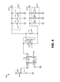
- FIG. 4 illustrates a circuit diagram of a system 400 for decreasing voltage droop in a USB power circuit configured to power multiple USB devices.
- System 400 may be implemented on a single circuit board or may be distributed across multiple circuit boards.
- System 400 represents at least a portion of a USB power circuit. It should be understood that similar systems may be used to decrease the amount of voltage droop for other types of direct current power circuits, particularly those in which a capacitive load may be initially connected while another device is being powered.
- System 400 may represent an embodiment of system 100, system 200, and/or system 300 of FIGS. 1 to 3 , respectively.
- System 400 may receive a DC voltage from an external source or may generate the DC voltage from another AC or DC voltage source.
- voltage source 405 is a +5 V DC power source.
- Voltage source 405 may represent voltage source 110 of FIGS. 1 to 3 .
- Power switch 410 may serve to regulate current drawn from voltage source 405.
- Power switch 410 may decouple voltage source 405 from transformer 415 when certain conditions are satisfied, such as an excess of current being drawn or a temperature has been exceeded.
- MP6211DN manufactured by MPS may be used for power switch 410.
- voltage source 110 may represent both voltage source 405 and power switch 410.
- Transformer 415 may represent the transformer of transformer module 120-1 of FIGS. 1 to 3 .
- Transformer 415 may be a dual-winding transformer having a 1:1 winding ratio.
- Transformer 415 may be wired such that current flows from terminal 1 to terminal 2 through winding 416, and that current flows from terminal 3 to terminal 4 through winding 417.
- an increase in current through either of winding 416 or winding 417 results in an increase in current and/or voltage through the other winding, as wired.
- transformer 415 may be TAIYO YUDEN CM04RC.
- Resistor 420 may represent resistor 330 of FIG. 3 and may be part of a transformer module. Resistor 420 may serve to regulate the amount of current and/or voltage induced by winding 416 and winding 417 in the other winding.
- the resistance of resistor 420 may be (at least approximately) four times the impedance of voltage source 405 (the 4:1 ratio is examined later in this document). Other values of resistor 420 may also be used. In some examples, a resistance of 1 Ohm is used for resistor 420, such as when the impedance of the voltage source is 0.25 Ohms.
- transformer module 120-1 may represent both transformer 415 and resistor 420.
- Outputs 430 may be electrically coupled with resistor 420, transformer 415, power switch 410, and voltage source 405. Outputs 430 may represent outputs 130 of FIGS. 1 to 3 . If system 400 is a USB power supply circuit, outputs 430 may represent USB power output ports. Output 430-1 may be electrically connected with capacitor module 435-1, which includes capacitors 436-1, 437-1, and 438-1. Output 430-2 may be electrically connected with capacitor module 435-2, which includes capacitors 436-2, 437-2, and 438-2. Capacitors 436 may have a capacitance of 10 ⁇ F. Capacitors 437 may have a capacitance of 100 ⁇ F. Capacitors 438 may have a capacitance of 0.1 ⁇ F. As such, the total capacitance of each of capacitor modules 435 may be less than the minimum of 120-1 ⁇ F required for a USB power supply by USB specifications.
- a USB device may be connected with each of outputs 430.
- USB device(s) may be connected with either output 430-1, output 430-2, both, or neither.
- the USB device due to its capacitance, may, upon connection with output 430-2, behave as a capacitive load, and thus draw an inrush current from voltage source 405 via power switch 410 and winding 417.
- the inrush current drawn by the USB device connected with output 430-1 may be supplied, at least in part, by: capacitor module 435-1 and voltage source 405.
- the draw of the inrush current by the USB device connected with output 430-2 may result in voltage droop on output 430-1.
- the amount of voltage droop experienced by output 430-1 may be decreased due to capacitor modules 435 and additional voltage and/or current being supplied by transformer 415 via winding 416 (due to the magnetic flux generated by the current flowing through winding 417). As such, voltage droop on output 430-1 is at least partially mitigated due to transformer 415 and capacitor modules 435.
- the USB device due to its capacitance, may, upon connection with output 430-1, behave as a capacitive load, and thus draw an inrush current from voltage source 405 via power switch 410 and winding 416 of transformer 415.
- the current drawn by the USB device already connected with output 430-2 may be supplied, at least in part, by: capacitor module 435-2 and voltage source 405.
- the draw of the inrush current by the USB connected with output 430-1 may result in voltage droop on output 430-2.
- the amount of voltage droop experienced by output 430-2 may be decreased due to capacitor modules 435 and additional voltage and/or current being supplied by transformer 415 via winding 417 (due to the magnetic flux generated by the current flowing through winding 416). As such, voltage droop on output 430-2 is at least partially mitigated due to transformer 415 and capacitor modules 435.
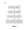
- FIG. 5 illustrates a method for mitigating voltage droop in a direct current circuit configured to power multiple capacitive loads.
- Method 500 may be performed using one of systems 100 through 400 of FIGS. 1 to 4 , respectively, Method 500 may also be performed using a different system configured for mitigating voltage droop in a DC circuit that is configured to power multiple capacitive loads.
- Means for performing each step of method 500 include systems 100 through 400 and their respective components.
- a transformer may be electrically coupled with a direct current voltage source and a first and second output.
- the transformer may be electrically coupled with the voltage source through one or more additional components.
- transformer 415 is electrically coupled with voltage source 405 via power switch 410.
- the transformer used at step 510 may be a tapped single winding transformer or a dual winding transformer.
- the transformer may have a winding ratio of 1:1.
- the transformer may have each winding electrically coupled with the voltage source and each winding may be electrically coupled with an output.
- the transformer may be coupled with the voltage source such that current drawn by a capacitive load placed on an output through the windings of the transformer flow in opposite directions. As such, an increased current to one output will cause an increase in voltage to the other output.
- an output DC voltage may be provided to a first capacitive load connected with the first voltage output.
- This first capacitive load may use the received voltage as a power source.
- no capacitive load may be connected with the second output.
- the voltage source may currently only be used for powering the first capacitive load connected with the first voltage output.
- a second capacitive load may be connected with the second output.
- the voltage source may supply this second capacitive load with a voltage (and thus current) to power the second capacitive load. Due to the voltage source not being ideal, it may not be able to provide a perfect steady-state DC voltage to the first capacitive load when the second capacitive load is connected due to the amount of initial inrush current being drawn by the second capacitive load.
- the first capacitive load may experience voltage droop on the first output due to the inrush current being drawn by the second capacitive load via the second output.
- the amount of droop in voltage output to the first capacitive load via the first output may be at least partially mitigated.
- the voltage droop may be mitigated by the transformer action, the phasing of the transaction windings, and/or the compensation impedance (such as provided by resistor 420 of FIG. 4 ).
- the amount of voltage droop experienced by the first output connected with the first capacitive load is less than if the transformer was not electrically coupled with the circuit at step 510.
- the voltage supply may provide each of the first and second outputs with a steady state DC voltage at approximately the voltage output by the voltage source.
- method 500 may repeat.
- FIG. 6 illustrates a method 600 for decreasing voltage droop in a USB power circuit configured to power multiple USB devices.
- Method 600 may be performed using one of systems 100 through 400 of FIGS 1 to 4 , respectively.
- Method 600 may also be performed using a different system configured for mitigating voltage droop in a DC circuit that is configured to power multiple capacitive loads.
- Method 600 may represent an alternative embodiment of method 500.
- Means for performing each step of method 600 include systems 100 through 400 and their respective components.
- a transformer may be electrically coupled with a direct current voltage source and a first USB power output and a second USB power output.
- the transformer may be electrically coupled with the voltage source through one or more additional components.
- transformer 415 is electrically coupled with voltage source 405 via power switch 410.
- the transformer used at step 510 may be a tapped single winding transformer or a dual winding transformer.
- the transformer may have a winding ratio of 1:1.
- the transformer may have each winding electrically coupled with the voltage source and each winding may be electrically coupled with an output.
- the transformer may be coupled with the voltage source such that current drawn by a capacitive load placed on an output through the windings of the transformer flow in opposite directions.
- one or more resistors may be electrically coupled between the first output and the second output. These one or more resistors may be used to control the amount of voltage and/or current inducted by the transformer on one USB power output when a capacitive load draws an inrush current on the other USB power output.
- the one or more resistors may have a resistance of (approximately) four times the impedance of the voltage source.
- the voltage source impedance may be 0.25 Ohms, thus the resistance of the resistor(s) may be 1 Ohm. Analysis detailed later in this document indicates how the resistance value of four times the voltage source impedance is arrived at.
- one or more capacitors may be coupled with each of the first and second USB power outputs. Such capacitors may be used together with the transformer to mitigate voltage droop when the second USB device is connected with the second USB power output. According to USB specifications, at least 120 ⁇ F of capacitance is required to be coupled with each USB power output so that no more than 330 mV of voltage droop is experienced on a USB power output when a USB device (which is acting as a capacitive load) is connected with another USB power output that is electrically coupled with the same voltage source.
- capacitors that have less than a total of 120 ⁇ F of capacitance while achieving less than a maximum of 330 mV of voltage droop on a USB power output when a USB device is connected with another USB power output connected with the same voltage source.
- 110.1 ⁇ F of capacitance may be electrically coupled with each USB power output.
- Such capacitance may be in the form of: one 100 ⁇ F capacitor, one 10 ⁇ F capacitor, and one 0.1 ⁇ F capacitor.
- an output DC voltage of +5 V may be provided to a first USB device connected with the first USB power output.
- This USB device may use the received 5 V DC as a power source.
- no USB device may be connected with the second USB power output.
- the voltage source may currently only be used for powering the first USB device connected with the first USB power output.
- a second USB device may be connected with the second USB power output.
- the voltage source may attempt to supply this second USB device with a +5 V DC voltage. Due to the voltage source not being ideal, it may not be able to provide a perfect steady-state DC voltage to the first USB device when the second USB device is initially connected to the second USB power output due to the amount of inrush current being drawn by the second USB device, which is acting as a capacitive load. As such, the first USB device may experience voltage droop on the first USB power output due to the current being drawn by the second USB device via the second output.
- the amount of droop in voltage output to the first USB device via the first USB power output may be at least partially mitigated.
- the voltage droop may be mitigated by the transformer being induced by the current through the second winding to the second USB power output to output a greater voltage to the first USB power output.
- the amount of voltage droop experienced by the first USB power output connected with the first USB device is less than if the transformer was not electrically coupled with the circuit at step 610.
- the voltage droop to the first USB device may be further mitigated by capacitors being present on the first and second USB power outputs.
- Current drawn by the second USB device may at least partially supplied by the capacitors coupled with the second USB power output thus decreasing the amount of current drawn by the second USB device through the transformer from the voltage supply.
- Capacitors coupled with the first USB power output may also help mitigate voltage droop to the first USB device.
- the capacitors may work in combination with the transformer to mitigate voltage droop output by the first USB power output to the first USB device.
- the voltage supply may provide the first and second outputs with a steady state +5 V DC.
- method 600 may repeat. It should be understood that if the first USB device is disconnected from the first USB power output and the first USB device (or another USB device) is then (re)connected to the first USB power output, references to the "first" and "second" in steps 640 through 660 would be reversed.
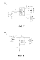
- FIGS. 7 to 11 detail how the 4:1 ratio of impedance across transformer to voltage source impedance may be calculated.
- FIG. 7 illustrates a circuit 700, similar to systems 200 through 400 of FIGS. 2 to 4 , respectively, where a capacitive load (initially having zero voltage) is connected with a circuit having a transformer module including a transformer and impedance (e.g., a resistor) across the outputs of the circuit.
- Circuit 800 of FIG. 8 represents circuit 700 of FIG. 7 redrawn to facilitate a transient analysis.
- FIG. 9 shows the voltages in a transformer, such as the transformer of FIGS. 7 and 8 .
- FIG. 10 illustrates an ideal 1:1 transformer 1000.
- Transformer 1000 illustrates the transformer action of the primary voltage being coupled to the secondary voltage and the primary current being coupled to the secondary current.
- L represents the mutual inductance.
- FIG. 11 illustrates circuit 1100, which is a combination of transformer 1000 being used to represent the transformer in circuit 800 of FIG. 8 . As such, circuit 1100 represents circuit 700.
- the capacitive load is represented C , and its voltage by V C .
- the capacitive load already connected with circuit 1100 is represented by Z LOAD , with the voltage across Z LOAD being V LOAD .
- Z S represents the voltage source impedance.
- the switch, S may be closed, thus connecting capacitive load C to with the remainder of circuit 1100.
- this 4:1 ratio of compensating impedance Z C to source impedance Z S may change.
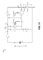
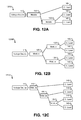
- FIGS. 12A to 12E illustrate examples 1200A to 1200E of how greater numbers of capacitive loads may be connected with a single voltage source and utilize similar circuits as described herein to increase or maximize isolation between capacitive loads.
- transformer modules 120 labeled “modules” for short
- Each of transformer modules 120 which may contain a transformer and one or more resistors, such as illustrated in FIG. 3 , may be connected as shown to isolate multiple capacitive loads.
- Each module may represent a transformer with an impedance (e.g., one or more resistors) across the transformer, such as illustrated in FIG. 3 .
- circuit 1200A contains two transformer modules 120-1 and 120-2 that may be connected as shown to isolate three capacitive loads (140-1, 140-2, and 140-3) from each other. As such, the outputs of transformer module 120-1 are connected with another transformer module 120-2 and capacitive load 140-1, respectively. The outputs of transformer module 120-2 are connected with capacitive loads 140-2 and 140-3.
- circuit 1200B contains three transformer modules that may be connected in a hierarchy to isolate four capacitive loads. The outputs of transformer module 120-1 may be connected with transformer modules 120-2 and 120-3. The outputs of transformer modules 120-2 and 120-3 may each be connected with a capacitive load of capacitive loads 140.
- FIG. 12A circuit 1200A contains two transformer modules 120-1 and 120-2 that may be connected as shown to isolate three capacitive loads (140-1, 140-2, and 140-3) from each other. As such, the outputs of transformer module 120-1 are connected with another transformer module 120-2 and capacitive load 140-1, respectively. The outputs of transformer module 120-2 are connected with capac
- circuit 1200C contains a cascade of transformer modules that may be connected such that an output of each transformer module is connected to a capacitive load and the other output of each transformer module is connected to another transformer module (with the outputs of transformer module 120-3 each being connected to a capacitive load).
- circuit 1200D contains an odd number of capacitive loads that are isolated by using a hierarchy of transformer modules.
- the outputs of transformer module 120-1 are connected to transformer modules 120-2 and 120-3.
- One output of transformer module 120-3 is connected to the voltage input of transformer module 120-4.
- the remaining outputs of the transformer modules are each connected to a capacitive load of capacitive loads 140.
- FIG. 12C circuit 1200C contains a cascade of transformer modules that may be connected such that an output of each transformer module is connected to a capacitive load and the other output of each transformer module is connected to another transformer module (with the outputs of transformer module 120-3 each being connected to a capacitive load).
- circuit 1200D contains an odd number of capacitive loads that
- circuit 1200E contains five capacitive loads which are isolated using a cascade arrangements of transformer modules 120 similar to circuit 1200C. It should be understood that different numbers of capacitive loads may be isolated using circuit arrangements as detailed in FIGS. 12A to 12E .
- USB power circuits focuses on USB power circuits; however, it should be understood that various embodiments described herein may be adapted to mitigate voltage droop for other forms of DC circuits where a capacitive load may be electrically coupled with a voltage supply while the voltage supply is providing a voltage to another output.
- embodiments may be described as a method which is depicted as a flow diagram or block diagram. Although each may describe the operations as a sequential process, many of the operations can be performed in parallel or concurrently. In addition, the order of the operations may be rearranged. A process may have additional steps not included in the figure. Furthermore, embodiments of the methods may be implemented by hardware, firmware, or any combination thereof.
Applications Claiming Priority (2)
| Application Number | Priority Date | Filing Date | Title |
|---|---|---|---|
| US201261616557P | 2012-03-28 | 2012-03-28 | |
| US13/569,800 US9244511B2 (en) | 2012-03-28 | 2012-08-08 | Transient electrical load decoupling for a direct current power supply |
Publications (3)
| Publication Number | Publication Date |
|---|---|
| EP2645203A2 true EP2645203A2 (de) | 2013-10-02 |
| EP2645203A3 EP2645203A3 (de) | 2016-03-23 |
| EP2645203B1 EP2645203B1 (de) | 2018-04-25 |
Family
ID=47997226
Family Applications (1)
| Application Number | Title | Priority Date | Filing Date |
|---|---|---|---|
| EP13161547.8A Active EP2645203B1 (de) | 2012-03-28 | 2013-03-28 | System und Verfahren zur Abschwächung eines Spannungsabfalls in Gleichstromkreis |
Country Status (2)
| Country | Link |
|---|---|
| US (2) | US9244511B2 (de) |
| EP (1) | EP2645203B1 (de) |
Cited By (1)
| Publication number | Priority date | Publication date | Assignee | Title |
|---|---|---|---|---|
| US10552250B2 (en) | 2017-10-10 | 2020-02-04 | International Business Machines Corporation | Proactive voltage droop reduction and/or mitigation in a processor core |
Families Citing this family (5)
| Publication number | Priority date | Publication date | Assignee | Title |
|---|---|---|---|---|
| US9244511B2 (en) | 2012-03-28 | 2016-01-26 | Echostar Uk Holdings Limited | Transient electrical load decoupling for a direct current power supply |
| KR101809787B1 (ko) * | 2015-03-10 | 2017-12-15 | 엘에스산전 주식회사 | 배터리 전력 공급 시스템을 포함하는 전력 공급 시스템 |
| US10528112B2 (en) * | 2016-09-11 | 2020-01-07 | Microsemi P.O.E. Ltd. | MPS generation system and method |
| CN106599341B (zh) * | 2016-10-21 | 2020-04-14 | 南方电网科学研究院有限责任公司 | 含柔性直流输电系统的安稳控制策略表生成方法 |
| CN112600235B (zh) * | 2020-12-08 | 2021-08-03 | 广东电网有限责任公司阳江供电局 | 一种柔性直流换流器等效阻抗的优化控制方法和装置 |
Family Cites Families (13)
| Publication number | Priority date | Publication date | Assignee | Title |
|---|---|---|---|---|
| US4888675A (en) * | 1987-08-26 | 1989-12-19 | Harris Corporation | Switching power supply filter |
| JP3480438B2 (ja) * | 2000-09-07 | 2003-12-22 | 松下電器産業株式会社 | 多出力スイッチング電源装置 |
| FR2817436B1 (fr) * | 2000-11-30 | 2003-02-07 | Cit Alcatel | Dispositif de raccordement d'une ligne d'abonne a une liaison haute frequence et a une liaison basse frequence |
| JP3962735B2 (ja) * | 2004-09-07 | 2007-08-22 | Tdk株式会社 | 信号伝送回路、電子機器、ケーブル、及びコネクタ |
| US7531917B2 (en) * | 2006-05-10 | 2009-05-12 | Powercart Systems, Inc. | Mobile power supply |
| US20090102442A1 (en) * | 2007-10-18 | 2009-04-23 | Li-Chun Lai | Power Supply Device for USB |
| TWI384354B (zh) * | 2008-11-14 | 2013-02-01 | Ampower Technology Co Ltd | 具有低待機功率的電源裝置 |
| US8487476B2 (en) * | 2009-03-09 | 2013-07-16 | Ramin Rostami | Apparatus and methods for powering mobile devices |
| CN101963835B (zh) * | 2009-07-24 | 2013-04-24 | 鸿富锦精密工业(深圳)有限公司 | 动态分配usb端口电源的电子设备及方法 |
| US20110169474A1 (en) * | 2010-01-09 | 2011-07-14 | Cuks, Llc | Step-down switching PFC converter |
| JP5283719B2 (ja) * | 2011-02-16 | 2013-09-04 | シャープ株式会社 | 電子機器及び電子機器システム |
| US9244511B2 (en) | 2012-03-28 | 2016-01-26 | Echostar Uk Holdings Limited | Transient electrical load decoupling for a direct current power supply |
| KR101428199B1 (ko) * | 2012-10-22 | 2014-08-07 | 엘지이노텍 주식회사 | 공통모드필터 및 이를 포함하는 전원 공급 장치 |
-
2012
- 2012-08-08 US US13/569,800 patent/US9244511B2/en active Active
-
2013
- 2013-03-28 EP EP13161547.8A patent/EP2645203B1/de active Active
-
2015
- 2015-12-16 US US14/970,861 patent/US9935457B2/en active Active
Non-Patent Citations (1)
| Title |
|---|
| None |
Cited By (3)
| Publication number | Priority date | Publication date | Assignee | Title |
|---|---|---|---|---|
| US10552250B2 (en) | 2017-10-10 | 2020-02-04 | International Business Machines Corporation | Proactive voltage droop reduction and/or mitigation in a processor core |
| US11275644B2 (en) | 2017-10-10 | 2022-03-15 | International Business Machines Corporation | Proactive voltage droop reduction and/or mitigation in a processor core |
| US11693728B2 (en) | 2017-10-10 | 2023-07-04 | International Business Machines Corporation | Proactive voltage droop reduction and/or mitigation in a processor core |
Also Published As
| Publication number | Publication date |
|---|---|
| US20130257151A1 (en) | 2013-10-03 |
| US9935457B2 (en) | 2018-04-03 |
| EP2645203A3 (de) | 2016-03-23 |
| US9244511B2 (en) | 2016-01-26 |
| EP2645203B1 (de) | 2018-04-25 |
| US20160099563A1 (en) | 2016-04-07 |
Similar Documents
| Publication | Publication Date | Title |
|---|---|---|
| US9935457B2 (en) | Transient electrical load decoupling for a direct current power supply | |
| US9768680B2 (en) | Power converter having EMI filter common to multiple converters | |
| US7466573B2 (en) | Method and apparatus for integrated active-diode-ORing and soft power switching | |
| US9401658B2 (en) | Power supply apparatus and method of generating power by the same | |
| US9203296B2 (en) | Power supply systems with filters | |
| EP2020725A2 (de) | Unterbrechungsfreie Online-Stromversorgung | |
| CN103915863B (zh) | 终端设备及其供电方法 | |
| JP2008301585A (ja) | ノイズフィルタ回路を備えた電気機器 | |
| WO2022121828A1 (zh) | 一种功率变换电路、功率变换电路的控制方法以及变压器 | |
| JP2021108514A (ja) | ノイズフィルタ装置及び電力システム | |
| US10333410B2 (en) | Common-mode (CM) electromagnetic interference (EMI) reduction in resonant converters | |
| US7531918B2 (en) | Hot insertion and extraction of power supply module | |
| US20130307324A1 (en) | Energy supply network; method and aircraft or spacecraft | |
| US10134526B2 (en) | Sheet formed inductive winding | |
| KR102660347B1 (ko) | 누설전류를 감소시킬 수 있는 충전 시스템 | |
| CN210297543U (zh) | 一种电源控制器的供电电路 | |
| KR102427627B1 (ko) | 복수 개의 부하장비를 구비한 시스템에서 돌입전류 제한회로 배치 구조 및 이 구조를 포함하는 시스템 | |
| JP5396309B2 (ja) | 給電装置 | |
| EP2959580B1 (de) | Stromversorgungen mit multitap-spannungsdämpfern und verfahren für eine stromversorgungseinrichtung | |
| CN210517886U (zh) | 一种供电电路 | |
| EP3322063B1 (de) | Mehrkanaliger wechselrichter für eine photovoltaische vorrichtung | |
| CN107258052B (zh) | 用于多个并联驱动器的插入电感器布置 | |
| CN103606899B (zh) | 具有电芯平衡功能的电池保护电路及电池系统 | |
| Soderberg et al. | Compatibility analysis of space qualified intermediate bus converter and point of load regulators for digital loads | |
| KR101684621B1 (ko) | 래치업 방지 장치 및 이를 구비한 제어기 |
Legal Events
| Date | Code | Title | Description |
|---|---|---|---|
| PUAI | Public reference made under article 153(3) epc to a published international application that has entered the european phase |
Free format text: ORIGINAL CODE: 0009012 |
|
| AK | Designated contracting states |
Kind code of ref document: A2 Designated state(s): AL AT BE BG CH CY CZ DE DK EE ES FI FR GB GR HR HU IE IS IT LI LT LU LV MC MK MT NL NO PL PT RO RS SE SI SK SM TR |
|
| AX | Request for extension of the european patent |
Extension state: BA ME |
|
| PUAL | Search report despatched |
Free format text: ORIGINAL CODE: 0009013 |
|
| AK | Designated contracting states |
Kind code of ref document: A3 Designated state(s): AL AT BE BG CH CY CZ DE DK EE ES FI FR GB GR HR HU IE IS IT LI LT LU LV MC MK MT NL NO PL PT RO RS SE SI SK SM TR |
|
| AX | Request for extension of the european patent |
Extension state: BA ME |
|
| RIC1 | Information provided on ipc code assigned before grant |
Ipc: G06F 1/26 20060101ALI20160215BHEP Ipc: G06F 1/30 20060101AFI20160215BHEP |
|
| 17P | Request for examination filed |
Effective date: 20160916 |
|
| RBV | Designated contracting states (corrected) |
Designated state(s): AL AT BE BG CH CY CZ DE DK EE ES FI FR GB GR HR HU IE IS IT LI LT LU LV MC MK MT NL NO PL PT RO RS SE SI SK SM TR |
|
| RAP1 | Party data changed (applicant data changed or rights of an application transferred) |
Owner name: ECHOSTAR TECHNOLOGIES L.L.C. |
|
| GRAP | Despatch of communication of intention to grant a patent |
Free format text: ORIGINAL CODE: EPIDOSNIGR1 |
|
| STAA | Information on the status of an ep patent application or granted ep patent |
Free format text: STATUS: GRANT OF PATENT IS INTENDED |
|
| INTG | Intention to grant announced |
Effective date: 20171215 |
|
| GRAS | Grant fee paid |
Free format text: ORIGINAL CODE: EPIDOSNIGR3 |
|
| GRAA | (expected) grant |
Free format text: ORIGINAL CODE: 0009210 |
|
| STAA | Information on the status of an ep patent application or granted ep patent |
Free format text: STATUS: THE PATENT HAS BEEN GRANTED |
|
| AK | Designated contracting states |
Kind code of ref document: B1 Designated state(s): AL AT BE BG CH CY CZ DE DK EE ES FI FR GB GR HR HU IE IS IT LI LT LU LV MC MK MT NL NO PL PT RO RS SE SI SK SM TR |
|
| REG | Reference to a national code |
Ref country code: GB Ref legal event code: FG4D |
|
| REG | Reference to a national code |
Ref country code: CH Ref legal event code: EP |
|
| REG | Reference to a national code |
Ref country code: AT Ref legal event code: REF Ref document number: 993572 Country of ref document: AT Kind code of ref document: T Effective date: 20180515 |
|
| REG | Reference to a national code |
Ref country code: IE Ref legal event code: FG4D |
|
| REG | Reference to a national code |
Ref country code: DE Ref legal event code: R096 Ref document number: 602013036347 Country of ref document: DE |
|
| REG | Reference to a national code |
Ref country code: NL Ref legal event code: FP |
|
| REG | Reference to a national code |
Ref country code: LT Ref legal event code: MG4D |
|
| PG25 | Lapsed in a contracting state [announced via postgrant information from national office to epo] |
Ref country code: NO Free format text: LAPSE BECAUSE OF FAILURE TO SUBMIT A TRANSLATION OF THE DESCRIPTION OR TO PAY THE FEE WITHIN THE PRESCRIBED TIME-LIMIT Effective date: 20180725 Ref country code: LT Free format text: LAPSE BECAUSE OF FAILURE TO SUBMIT A TRANSLATION OF THE DESCRIPTION OR TO PAY THE FEE WITHIN THE PRESCRIBED TIME-LIMIT Effective date: 20180425 Ref country code: BG Free format text: LAPSE BECAUSE OF FAILURE TO SUBMIT A TRANSLATION OF THE DESCRIPTION OR TO PAY THE FEE WITHIN THE PRESCRIBED TIME-LIMIT Effective date: 20180725 Ref country code: FI Free format text: LAPSE BECAUSE OF FAILURE TO SUBMIT A TRANSLATION OF THE DESCRIPTION OR TO PAY THE FEE WITHIN THE PRESCRIBED TIME-LIMIT Effective date: 20180425 Ref country code: SE Free format text: LAPSE BECAUSE OF FAILURE TO SUBMIT A TRANSLATION OF THE DESCRIPTION OR TO PAY THE FEE WITHIN THE PRESCRIBED TIME-LIMIT Effective date: 20180425 Ref country code: PL Free format text: LAPSE BECAUSE OF FAILURE TO SUBMIT A TRANSLATION OF THE DESCRIPTION OR TO PAY THE FEE WITHIN THE PRESCRIBED TIME-LIMIT Effective date: 20180425 Ref country code: ES Free format text: LAPSE BECAUSE OF FAILURE TO SUBMIT A TRANSLATION OF THE DESCRIPTION OR TO PAY THE FEE WITHIN THE PRESCRIBED TIME-LIMIT Effective date: 20180425 |
|
| PG25 | Lapsed in a contracting state [announced via postgrant information from national office to epo] |
Ref country code: GR Free format text: LAPSE BECAUSE OF FAILURE TO SUBMIT A TRANSLATION OF THE DESCRIPTION OR TO PAY THE FEE WITHIN THE PRESCRIBED TIME-LIMIT Effective date: 20180726 Ref country code: HR Free format text: LAPSE BECAUSE OF FAILURE TO SUBMIT A TRANSLATION OF THE DESCRIPTION OR TO PAY THE FEE WITHIN THE PRESCRIBED TIME-LIMIT Effective date: 20180425 Ref country code: RS Free format text: LAPSE BECAUSE OF FAILURE TO SUBMIT A TRANSLATION OF THE DESCRIPTION OR TO PAY THE FEE WITHIN THE PRESCRIBED TIME-LIMIT Effective date: 20180425 Ref country code: LV Free format text: LAPSE BECAUSE OF FAILURE TO SUBMIT A TRANSLATION OF THE DESCRIPTION OR TO PAY THE FEE WITHIN THE PRESCRIBED TIME-LIMIT Effective date: 20180425 |
|
| REG | Reference to a national code |
Ref country code: AT Ref legal event code: MK05 Ref document number: 993572 Country of ref document: AT Kind code of ref document: T Effective date: 20180425 |
|
| PG25 | Lapsed in a contracting state [announced via postgrant information from national office to epo] |
Ref country code: PT Free format text: LAPSE BECAUSE OF FAILURE TO SUBMIT A TRANSLATION OF THE DESCRIPTION OR TO PAY THE FEE WITHIN THE PRESCRIBED TIME-LIMIT Effective date: 20180827 |
|
| REG | Reference to a national code |
Ref country code: DE Ref legal event code: R097 Ref document number: 602013036347 Country of ref document: DE |
|
| PG25 | Lapsed in a contracting state [announced via postgrant information from national office to epo] |
Ref country code: DK Free format text: LAPSE BECAUSE OF FAILURE TO SUBMIT A TRANSLATION OF THE DESCRIPTION OR TO PAY THE FEE WITHIN THE PRESCRIBED TIME-LIMIT Effective date: 20180425 Ref country code: AT Free format text: LAPSE BECAUSE OF FAILURE TO SUBMIT A TRANSLATION OF THE DESCRIPTION OR TO PAY THE FEE WITHIN THE PRESCRIBED TIME-LIMIT Effective date: 20180425 Ref country code: EE Free format text: LAPSE BECAUSE OF FAILURE TO SUBMIT A TRANSLATION OF THE DESCRIPTION OR TO PAY THE FEE WITHIN THE PRESCRIBED TIME-LIMIT Effective date: 20180425 Ref country code: CZ Free format text: LAPSE BECAUSE OF FAILURE TO SUBMIT A TRANSLATION OF THE DESCRIPTION OR TO PAY THE FEE WITHIN THE PRESCRIBED TIME-LIMIT Effective date: 20180425 Ref country code: RO Free format text: LAPSE BECAUSE OF FAILURE TO SUBMIT A TRANSLATION OF THE DESCRIPTION OR TO PAY THE FEE WITHIN THE PRESCRIBED TIME-LIMIT Effective date: 20180425 Ref country code: SK Free format text: LAPSE BECAUSE OF FAILURE TO SUBMIT A TRANSLATION OF THE DESCRIPTION OR TO PAY THE FEE WITHIN THE PRESCRIBED TIME-LIMIT Effective date: 20180425 |
|
| PG25 | Lapsed in a contracting state [announced via postgrant information from national office to epo] |
Ref country code: SM Free format text: LAPSE BECAUSE OF FAILURE TO SUBMIT A TRANSLATION OF THE DESCRIPTION OR TO PAY THE FEE WITHIN THE PRESCRIBED TIME-LIMIT Effective date: 20180425 Ref country code: IT Free format text: LAPSE BECAUSE OF FAILURE TO SUBMIT A TRANSLATION OF THE DESCRIPTION OR TO PAY THE FEE WITHIN THE PRESCRIBED TIME-LIMIT Effective date: 20180425 |
|
| PLBE | No opposition filed within time limit |
Free format text: ORIGINAL CODE: 0009261 |
|
| STAA | Information on the status of an ep patent application or granted ep patent |
Free format text: STATUS: NO OPPOSITION FILED WITHIN TIME LIMIT |
|
| 26N | No opposition filed |
Effective date: 20190128 |
|
| PG25 | Lapsed in a contracting state [announced via postgrant information from national office to epo] |
Ref country code: SI Free format text: LAPSE BECAUSE OF FAILURE TO SUBMIT A TRANSLATION OF THE DESCRIPTION OR TO PAY THE FEE WITHIN THE PRESCRIBED TIME-LIMIT Effective date: 20180425 |
|
| REG | Reference to a national code |
Ref country code: DE Ref legal event code: R082 Ref document number: 602013036347 Country of ref document: DE Representative=s name: HERNANDEZ, YORCK, DIPL.-ING., DE Ref country code: DE Ref legal event code: R081 Ref document number: 602013036347 Country of ref document: DE Owner name: DISH TECHNOLOGIES L.L.C., ENGLEWOOD, US Free format text: FORMER OWNER: ECHOSTAR TECHNOLOGIES L.L.C., ENGLEWOOD, COL., US |
|
| REG | Reference to a national code |
Ref country code: NL Ref legal event code: HC Owner name: DISH TECHNOLOGIES L.L.C.; US Free format text: DETAILS ASSIGNMENT: CHANGE OF OWNER(S), CHANGE OF OWNER(S) NAME; FORMER OWNER NAME: ECHOSTAR TECHNOLOGIES L.L.C. Effective date: 20190829 |
|
| PG25 | Lapsed in a contracting state [announced via postgrant information from national office to epo] |
Ref country code: MC Free format text: LAPSE BECAUSE OF FAILURE TO SUBMIT A TRANSLATION OF THE DESCRIPTION OR TO PAY THE FEE WITHIN THE PRESCRIBED TIME-LIMIT Effective date: 20180425 |
|
| REG | Reference to a national code |
Ref country code: CH Ref legal event code: PL |
|
| PG25 | Lapsed in a contracting state [announced via postgrant information from national office to epo] |
Ref country code: AL Free format text: LAPSE BECAUSE OF FAILURE TO SUBMIT A TRANSLATION OF THE DESCRIPTION OR TO PAY THE FEE WITHIN THE PRESCRIBED TIME-LIMIT Effective date: 20180425 Ref country code: LU Free format text: LAPSE BECAUSE OF NON-PAYMENT OF DUE FEES Effective date: 20190328 |
|
| REG | Reference to a national code |
Ref country code: BE Ref legal event code: MM Effective date: 20190331 |
|
| PG25 | Lapsed in a contracting state [announced via postgrant information from national office to epo] |
Ref country code: IE Free format text: LAPSE BECAUSE OF NON-PAYMENT OF DUE FEES Effective date: 20190328 Ref country code: LI Free format text: LAPSE BECAUSE OF NON-PAYMENT OF DUE FEES Effective date: 20190331 Ref country code: CH Free format text: LAPSE BECAUSE OF NON-PAYMENT OF DUE FEES Effective date: 20190331 |
|
| PG25 | Lapsed in a contracting state [announced via postgrant information from national office to epo] |
Ref country code: BE Free format text: LAPSE BECAUSE OF NON-PAYMENT OF DUE FEES Effective date: 20190331 |
|
| PG25 | Lapsed in a contracting state [announced via postgrant information from national office to epo] |
Ref country code: TR Free format text: LAPSE BECAUSE OF FAILURE TO SUBMIT A TRANSLATION OF THE DESCRIPTION OR TO PAY THE FEE WITHIN THE PRESCRIBED TIME-LIMIT Effective date: 20180425 |
|
| PG25 | Lapsed in a contracting state [announced via postgrant information from national office to epo] |
Ref country code: MT Free format text: LAPSE BECAUSE OF NON-PAYMENT OF DUE FEES Effective date: 20190328 |
|
| PG25 | Lapsed in a contracting state [announced via postgrant information from national office to epo] |
Ref country code: CY Free format text: LAPSE BECAUSE OF FAILURE TO SUBMIT A TRANSLATION OF THE DESCRIPTION OR TO PAY THE FEE WITHIN THE PRESCRIBED TIME-LIMIT Effective date: 20180425 |
|
| PG25 | Lapsed in a contracting state [announced via postgrant information from national office to epo] |
Ref country code: IS Free format text: LAPSE BECAUSE OF FAILURE TO SUBMIT A TRANSLATION OF THE DESCRIPTION OR TO PAY THE FEE WITHIN THE PRESCRIBED TIME-LIMIT Effective date: 20180825 |
|
| PG25 | Lapsed in a contracting state [announced via postgrant information from national office to epo] |
Ref country code: HU Free format text: LAPSE BECAUSE OF FAILURE TO SUBMIT A TRANSLATION OF THE DESCRIPTION OR TO PAY THE FEE WITHIN THE PRESCRIBED TIME-LIMIT; INVALID AB INITIO Effective date: 20130328 |
|
| PG25 | Lapsed in a contracting state [announced via postgrant information from national office to epo] |
Ref country code: MK Free format text: LAPSE BECAUSE OF FAILURE TO SUBMIT A TRANSLATION OF THE DESCRIPTION OR TO PAY THE FEE WITHIN THE PRESCRIBED TIME-LIMIT Effective date: 20180425 |
|
| PGFP | Annual fee paid to national office [announced via postgrant information from national office to epo] |
Ref country code: FR Payment date: 20230208 Year of fee payment: 11 |
|
| P01 | Opt-out of the competence of the unified patent court (upc) registered |
Effective date: 20230521 |
|
| PGFP | Annual fee paid to national office [announced via postgrant information from national office to epo] |
Ref country code: NL Payment date: 20240215 Year of fee payment: 12 |
|
| PGFP | Annual fee paid to national office [announced via postgrant information from national office to epo] |
Ref country code: DE Payment date: 20240130 Year of fee payment: 12 Ref country code: GB Payment date: 20240108 Year of fee payment: 12 |