EP2642544B1 - Anordnung aus einem Piezoaktor und einer flexiblen Leiterplatte - Google Patents
Anordnung aus einem Piezoaktor und einer flexiblen Leiterplatte Download PDFInfo
- Publication number
- EP2642544B1 EP2642544B1 EP12161026.5A EP12161026A EP2642544B1 EP 2642544 B1 EP2642544 B1 EP 2642544B1 EP 12161026 A EP12161026 A EP 12161026A EP 2642544 B1 EP2642544 B1 EP 2642544B1
- Authority
- EP
- European Patent Office
- Prior art keywords
- circuit board
- thick
- printed circuit
- layer electrode
- flexible printed
- Prior art date
- Legal status (The legal status is an assumption and is not a legal conclusion. Google has not performed a legal analysis and makes no representation as to the accuracy of the status listed.)
- Active
Links
Images


Classifications
-
- H—ELECTRICITY
- H10—SEMICONDUCTOR DEVICES; ELECTRIC SOLID-STATE DEVICES NOT OTHERWISE PROVIDED FOR
- H10N—ELECTRIC SOLID-STATE DEVICES NOT OTHERWISE PROVIDED FOR
- H10N30/00—Piezoelectric or electrostrictive devices
- H10N30/01—Manufacture or treatment
- H10N30/07—Forming of piezoelectric or electrostrictive parts or bodies on an electrical element or another base
-
- B—PERFORMING OPERATIONS; TRANSPORTING
- B06—GENERATING OR TRANSMITTING MECHANICAL VIBRATIONS IN GENERAL
- B06B—METHODS OR APPARATUS FOR GENERATING OR TRANSMITTING MECHANICAL VIBRATIONS OF INFRASONIC, SONIC, OR ULTRASONIC FREQUENCY, e.g. FOR PERFORMING MECHANICAL WORK IN GENERAL
- B06B1/00—Methods or apparatus for generating mechanical vibrations of infrasonic, sonic, or ultrasonic frequency
- B06B1/02—Methods or apparatus for generating mechanical vibrations of infrasonic, sonic, or ultrasonic frequency making use of electrical energy
- B06B1/06—Methods or apparatus for generating mechanical vibrations of infrasonic, sonic, or ultrasonic frequency making use of electrical energy operating with piezoelectric effect or with electrostriction
-
- G—PHYSICS
- G10—MUSICAL INSTRUMENTS; ACOUSTICS
- G10K—SOUND-PRODUCING DEVICES; METHODS OR DEVICES FOR PROTECTING AGAINST, OR FOR DAMPING, NOISE OR OTHER ACOUSTIC WAVES IN GENERAL; ACOUSTICS NOT OTHERWISE PROVIDED FOR
- G10K11/00—Methods or devices for transmitting, conducting or directing sound in general; Methods or devices for protecting against, or for damping, noise or other acoustic waves in general
- G10K11/004—Mounting transducers, e.g. provided with mechanical moving or orienting device
-
- H—ELECTRICITY
- H10—SEMICONDUCTOR DEVICES; ELECTRIC SOLID-STATE DEVICES NOT OTHERWISE PROVIDED FOR
- H10N—ELECTRIC SOLID-STATE DEVICES NOT OTHERWISE PROVIDED FOR
- H10N30/00—Piezoelectric or electrostrictive devices
- H10N30/01—Manufacture or treatment
- H10N30/06—Forming electrodes or interconnections, e.g. leads or terminals
-
- H—ELECTRICITY
- H10—SEMICONDUCTOR DEVICES; ELECTRIC SOLID-STATE DEVICES NOT OTHERWISE PROVIDED FOR
- H10N—ELECTRIC SOLID-STATE DEVICES NOT OTHERWISE PROVIDED FOR
- H10N30/00—Piezoelectric or electrostrictive devices
- H10N30/101—Piezoelectric or electrostrictive devices with electrical and mechanical input and output, e.g. having combined actuator and sensor parts
-
- H—ELECTRICITY
- H10—SEMICONDUCTOR DEVICES; ELECTRIC SOLID-STATE DEVICES NOT OTHERWISE PROVIDED FOR
- H10N—ELECTRIC SOLID-STATE DEVICES NOT OTHERWISE PROVIDED FOR
- H10N30/00—Piezoelectric or electrostrictive devices
- H10N30/80—Constructional details
- H10N30/87—Electrodes or interconnections, e.g. leads or terminals
- H10N30/875—Further connection or lead arrangements, e.g. flexible wiring boards, terminal pins
-
- Y—GENERAL TAGGING OF NEW TECHNOLOGICAL DEVELOPMENTS; GENERAL TAGGING OF CROSS-SECTIONAL TECHNOLOGIES SPANNING OVER SEVERAL SECTIONS OF THE IPC; TECHNICAL SUBJECTS COVERED BY FORMER USPC CROSS-REFERENCE ART COLLECTIONS [XRACs] AND DIGESTS
- Y10—TECHNICAL SUBJECTS COVERED BY FORMER USPC
- Y10T—TECHNICAL SUBJECTS COVERED BY FORMER US CLASSIFICATION
- Y10T29/00—Metal working
- Y10T29/42—Piezoelectric device making
Definitions
- the present invention relates to an arrangement of a piezoactuator and a flexible printed circuit board, with at least one electrical and mechanical connection between a first connection contact on the flexible printed circuit board and a second connection contact on the piezoelectric actuator, the connection being made through an opening in FIG the flexible printed circuit board is guided and wherein the surfaces of the connection contacts glued together have a substantially parallel and identically oriented normal vector.
- FIG. 6 The schematic structure of such a vibration level measuring device is in FIG. 6 shown.
- FIG. 6 The schematic structure in FIG. 6 is neither true to scale nor complete and is only intended to represent the function of a vibration level measuring device in the manner of a schematic diagram.
- the illustrated vibration level measuring device has a tuning fork 10, which is arranged on a membrane 9.
- the membrane 9 is part of the tuning fork 10, wherein tines 10 a, 10 b of the tuning fork 10 connected directly to the membrane 9 are and by bending the membrane 9 toward each other or moved away from each other.
- the membrane 9 is usually made of stainless steel and can be set in vibration via a piezoactuator 1.
- the piezoelectric actuator 1 is connected via a ceramic plate 7, which is arranged between the piezoelectric actuator 1 and the diaphragm 9, with this.
- the ceramic plate 7 is provided in order to adapt the different coefficients of thermal expansion of the membrane 9 and of the piezoelectric actuator 1 to one another.
- An underside of the piezoactuator 1 is metallized throughout, so that a voltage applied to the upper side causes a vibration of the piezoelectric actuator 1 due to a segmentation of the electrode on the upper side and a different polarization of these piezoelectric segments.
- the flexible printed circuit board 3 is in the present example as a so-called flex line, d. H. designed as a flexible spring-like printed circuit board with conductor tracks arranged thereon.
- the flexible printed circuit board 3 is connected to the points to be contacted of the piezoelectric actuator 1 with a conductive adhesive with this, so that only at the points connected by the adhesive, a voltage in the piezoelectric actuator 1 is initiated.
- the piezoelectric actuator 1 and the ceramic plate 7 and the membrane 9 are also glued together.
- the piezoactuator 1 is the first divided into four segments.
- the piezoelectric actuator 1 is generally formed circular in plan view and divided into four quadrants, which can be controlled individually by applying a voltage.
- To generate a vibration two diagonally opposite quadrants are each subjected to a voltage, while the other two quadrants are used to detect the generated oscillation. In this way, a vibration can be generated and detected simultaneously.
- the circuit board 3 is provided for applying the voltage with a first terminal contact 11, which is arranged corresponding to a second terminal contact 12 on the piezoelectric actuator 1.
- the first connection contact 11 on the printed circuit board 3 is usually arranged on the piezoelectric actuator 1 side facing the flexible printed circuit board 3, so that between the first terminal 11 and the second terminal contact 12 by applying a conductive adhesive and pressing the two components an electrically conductive Connection can be made.
- Another problem with this procedure is that incorrect alignment of the flexible printed circuit board 3 during the first startup can not be corrected, since otherwise the conductive adhesive between the terminal contacts 11, 12 smears and, as a consequence, also with short circuits between the individual quadrants of the piezoactuator 1 or the correspondingly arranged contacts of the flexible printed circuit board 3 is to be expected. It is also negative that the flexible printed circuit board 3 and the piezoelectric actuator 1 due to the intervening adhesive joint 5 can not be arranged directly on top of each other. Another negative is that pressed by pressing the flexible circuit board 3 and the piezoelectric actuator 1, the adhesive bonds therebetween flat and thus possibly excess adhesive is pushed out laterally next to the connection contacts 11, 12. This increases the risk of short circuits.
- the flexible printed circuit board 3 After application of the adhesive, the flexible printed circuit board 3 must be positioned plane-parallel and exactly to the piezoelectric actuator 1. For the reasons described above, a subsequent position correction is not possible.
- An inventive arrangement of a piezoelectric actuator 1 and a flexible printed circuit board has at least one produced by an electrically conductive adhesive electrical and mechanical connection between a first terminal contact on the circuit board and a second terminal contact on the piezoelectric actuator, wherein the connection through an opening in the Circuit board is guided and wherein the mutually bonded surfaces of the terminal contacts have a substantially parallel and equal-oriented normal vector and the second terminal contact consists of a thin-film electrode and at least one thick-film electrode.
- a rivet-like adhesive connection is created in this way, wherein the connection contacts are oriented in the same direction on the piezoelectric actuator to the flexible circuit board.
- an opening is provided through which the electrically conductive adhesive can be introduced for bonding, wherein it simultaneously covers the edges of the opening on the side facing away from the piezoelectric actuator side of the flexible printed circuit board creates a mushroom-shaped or rivet-like adhesive bond Compared to pure contact adhesives has a significantly increased mechanical stability.
- a particularly simple arrangement can be achieved if the thick-film electrode is arranged on the thin-film electrode.
- the thin film electrode applied by thin film technique e.g. a copper-nickel electrode with a layer thickness of less than 1 .mu.m, for example, by chemical vapor deposition or physical vapor deposition, such as vapor deposition or sputtering (sputtering) over the entire surface, selectively or in a lift-off process can be applied.
- a full-surface, as accurately as possible limited and reproducible metallization through the thin-film electrode is necessary in order to apply voltage to the piezoelectric actuator or individual quadrants of the piezoelectric actuator as fully as possible.
- a thick-film electrode for example a thick silver layer with a layer thickness of more than 10 ⁇ m, can then be applied to the thin-film electrode.
- the thick-film electrode can be applied, for example, by a screen printing process and then cured.
- the thick-film electrode can first be applied to the piezoelectric actuator and cured and then the thin-film electrode are applied to the full-surface voltage input.
- the thick-film electrode has a smaller area than the thin-film electrode. In this way, it is achieved that the electrically conductive adhesive is used only in the area of the smaller area of the thick-film electrode, and the current is injected into the piezoelectric actuator via the thin-film electrode which is additionally applied.
- a particularly simple and symmetrical configuration is achieved if the thick-film electrode is of circular design.
- a circular configuration of the thick-view electrode makes it particularly easy to achieve a closed outer edge of the thick-film electrode which is not interrupted by corner sections which would be present, for example, in the case of rectangular thick-film electrodes.
- the thick-film electrode may also be annular, in which case there is the advantage that a kind of "well” or “border” for the electrically conductive adhesive is additionally created by the annular thick-film electrode.
- the thick-film electrode has a first diameter which is greater than a diameter of the opening in the flexible printed circuit board. In this way, the flexible circuit board is completely on the edge of the thick-film electrode, thus creating a circumferential sealing edge.
- the first diameter of the thick-film electrode and the diameter of the opening in the flexible printed circuit board are preferably matched to one another such that a sufficient adhesive surface is created for a mechanical connection between the flexible printed circuit board and the piezoelectric actuator and at the same time a good sealing effect is achieved.
- the assembly described above can be produced particularly advantageously with a mounting aid, wherein the mounting aid is substantially plate-shaped and has at least one second opening in the region of at least one connection, wherein a second diameter of the second opening in the mounting aid and a first diameter of Thick-film electrode are matched to one another such that directed in the direction of the arrangement and acting on the flexible circuit board force acts on an edge of the thick-film electrode such that a seal against the adhesive is achieved.
- the flexible printed circuit board and the piezoelectric actuator are arranged relative to each other in a first step, the mounting aid aligned relative to the flexible printed circuit board, the flexible printed circuit board and the piezoelectric actuator with the aid of the assembly aid pressed together, the electrically conductive adhesive in the at least introduced and cured a first opening of the flexible circuit board.
- An aligning arrangement of the flexible printed circuit board and of the piezoelectric actuator in this context means that openings provided in the flexible printed circuit board are aligned as concentrically as possible with respect to the thick-film electrodes provided on the piezoelectric actuator.
- the mounting aid is arranged such that the openings in the mounting aid are aligned as concentric with the openings in the flexible circuit board and thus concentric with the underlying thick-film electrodes on the piezoelectric actuator.
- a preferred diameter for the thick-film electrode is 2.5 mm, wherein the diameter for the second opening in the mounting aid is then preferably 3.2 mm.
- FIG. 1 shows an arrangement of a piezoelectric actuator 1, on which a flexible circuit board 3 is arranged, wherein an electrical and mechanical connection between the flexible circuit board 3 and the piezoelectric actuator 1 is provided by an electrically conductive adhesive.
- the electrically conductive adhesive connects a first connection contact 11, which is annularly arranged on the side facing away from the piezoelectric actuator 1 side of the flexible printed circuit board 3, a first opening 4 in the flexible circuit board 3 is surrounded annularly.
- a second terminal contact 12 is arranged on the piezoelectric actuator 1 facing the flexible printed circuit board 3 and formed circular.
- Fine bumps in the piezoelectric actuator 1 or the flexible printed circuit board 3 cause fine gaps between these components, as a result of which high capillary forces suck the highly viscous, electrically conductive adhesive into the interspaces.
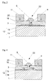
- FIG. 2 an arrangement according to the invention is shown, in which the second connection contact 12 is formed by a thin-film electrode 14 and a thick-film electrode 15 arranged on the thin-film 14.
- the thin-film electrode 14 serves for approximately full-surface electrical contacting of the piezoactuator 1, wherein the thick-film electrode 15 is arranged substantially in a region below the first opening 4 in the flexible printed circuit board 3.
- a first diameter d 1 of the thick-film electrode 15 in this region is slightly larger than a diameter d of the opening 4, through which electrically conductive adhesive for producing the electrical and mechanical connection 5 is filled.
- an assembly aid 20 is shown, which is used in the production of the inventive arrangement.
- the mounting aid 20 is substantially plate-shaped and has corresponding to the openings 4 in the flexible circuit board 3 formed second openings 22.
- a second diameter d 2 of the second openings 22 is chosen slightly larger than the first diameter d 1 of the thick-film electrode 15, so that a slight bending of the flexible printed circuit board 3 occurs by pressing the components during assembly and in a peripheral edge 16 of the thick-film electrode 15 a sealing effect for an introduced after the compression electrically conductive adhesive is achieved.
- the second diameter d 2 of the second opening 22 in the mounting aid 20 is preferably selected to be 28% larger than the first diameter d 1 of the thick-layer electrode 15.
- the first diameter d 1 of the thick-film electrode 15 is 2.5 mm and the second d 2 of the second opening 22 in the mounting aid 20 is 3.2 mm.
- the diameter d of the opening 4 in the flexible printed circuit board 3 is 1.2 mm in this embodiment.
- FIG. 3 shows a further embodiment of the inventive arrangement and the mounting aid 20th
- the thick-film electrode 15 is formed in two parts in the present embodiment, wherein a first part, analogous to FIG. 2 , is formed circular immediately below the opening 4 in the flexible printed circuit board 3.
- a first part analogous to FIG. 2
- an annular portion is provided which is spaced and the circular thick film electrode 15 is disposed surrounding.
- FIG. 4 shows a further alternative embodiment of the inventive arrangement.
- annular thick-facing electrode 15 is provided, which allows an increased sealing effect in the assembled state on the one hand at its peripheral edge 16 and at the same time in the interior of the ring a kind of "tub" for the introduced through the opening 4 in the flexible circuit board 3 electrically conductive adhesive. 5 forms.
- FIG. 5 shows the piezoelectric actuator 1 off FIG. 2 in plan view, wherein the piezoelectric actuator 1 as usual for the realization of a drive device for a limit level measuring device, divided into four segments.
- the four segments are each completely covered with the thin-film electrode 14, but have a sufficient distance from each other to ensure isolation of the segments against each other.
- a circular thick-film electrode 15 is arranged in each segment, each being delimited by a peripheral edge 16.
- the peripheral edge 16 ensures when mounting the arrangement according to the invention, the improved sealing effect against the electrically conductive adhesive, so that with the in the Figures 2 and 5
- a reduction of the short-circuit-related failures could be achieved from 19% to 3%.
- the short-circuit-related failure rate could even be reduced to 0%.
- the thin-film electrode 14 and the thick-film electrode 15 are applied to the piezoelectric actuator 1 in a suitable size.
- the thin-film electrode 14 is generally applied to the segments of the piezoactuator 1 over the entire area by chemical or physical vapor deposition.
- the thick-film electrodes 15 are subsequently
- the finished structured piezoelectric actuator 1 and the flexible printed circuit board 3 are then aligned relative to each other. Since the flexible printed circuit board 3 has openings 4 arranged corresponding to the thick-film electrodes 15, an alignment of flexible printed circuit board 3 and piezoelectric actuator 1 relative to one another means that the openings 4 are arranged above the respectively associated thick-film electrodes 15.
- the mutually aligned elements piezoelectric actuator 1 and flexible printed circuit board 3 are aligned for mounting relative to the mounting aid 20, ie the provided in the flexible circuit board 3 openings 4 are aligned concentrically with the second openings 22 in the mounting aid 20.
- an alignment of flexible printed circuit board 3 and piezoelectric actuator 1 can also take place on the basis of a permanently pre-assembled mounting aid 20.
- the predetermined amount of the conductive adhesive is dimensioned such that the first terminal contact 11, which surrounds the opening 4 in the flexible circuit board 3 annularly at least partially dome-like, so that a mushroom-shaped and rivet-shaped adhesive connection is formed, the same time the electrical connection between the first Terminal contact 11 and the second terminal contact 12 manufactures.
- the force expended for the compression can be dispensed with and the assembly aid 20 can be removed.
- the then firmly together mechanically and electrically connected components can then for further use in the arrangement according to FIG. 6 be used.
Landscapes
- Engineering & Computer Science (AREA)
- Manufacturing & Machinery (AREA)
- Mechanical Engineering (AREA)
- Physics & Mathematics (AREA)
- Acoustics & Sound (AREA)
- Multimedia (AREA)
- Particle Formation And Scattering Control In Inkjet Printers (AREA)
- Supporting Of Heads In Record-Carrier Devices (AREA)
- General Electrical Machinery Utilizing Piezoelectricity, Electrostriction Or Magnetostriction (AREA)
Description
- Die vorliegende Erfindung betrifft eine Anordnung aus einem Piezoaktor und einer flexiblen Leiterplatte, mit wenigstens einer durch einen elektrisch leitfähigen Klebstoff hergestellten elektrischen und mechanischen Verbindung zwischen einem ersten Anschlusskontakt an der flexiblen Leiterplatte und einem zweiten Anschlusskontakt an dem Piezoaktor, wobei die Verbindung durch eine Öffnung in der flexiblen Leiterplatte geführt ist und wobei die miteinander verklebten Oberflächen der Anschlusskontakte einen im wesentlichen parallel und gleich orientierten Normalenvektor aufweisen.
- Derartige Anordnungen, bei denen eine elektrische und mechanische Verbindung zwischen einer flexiblen Leiterplatte und einem Piezoaktor durch eine Klebeverbindung hergestellt wird, sind aus dem Stand der Technik bekannt und werden beispielsweise in sogenannten Vibrations-Grenzstandmessgeräten eingesetzt.
- Der schematische Aufbau eines solchen Vibrationsgrenzstandmessgerätes ist in
Figur 6 dargestellt. - Der schematische Aufbau in
Figur 6 ist weder maßstabsgetreu noch vollständig und soll lediglich nach Art einer Prinzipsskizze die Funktion eines Vibrations-Grenzstandmessgerätes darstellen. - Das dargestellte Vibrations-Grenzstandmessgerät weist eine Schwinggabel 10 auf, die an einer Membran 9 angeordnet ist. Die Membran 9 ist Teil der Schwinggabel 10, wobei Zinken 10a, 10b der Schwinggabel 10 direkt an der Membran 9 angebunden sind und durch Verbiegen der Membran 9 aufeinander zu- bzw. voneinander wegbewegt werden.
- Die Membran 9 ist in der Regel aus Edelstahl gefertigt und über einen Piezoaktor 1 in Schwingung versetzbar. Der Piezoaktor 1 ist über ein Keramikplättchen 7, das zwischen dem Piezoaktor 1 und der Membran 9 angeordnet ist, mit dieser verbunden. Das Keramikplättchen 7 ist vorgesehen, um die unterschiedlichen thermischen Ausdehnungskoeffizienten der Membran 9 und des Piezoaktors 1 einander anzupassen.
- Eine Erregung des Piezoaktors 1 erfolgt über eine elektrische Spannung, die über eine flexible Leiterplatte 3 an der Oberseite des Piezoaktors 1 angelegt wird. Eine Unterseite des Piezoaktors 1 ist durchgehend metallisiert, sodass eine an der Oberseite angelegte Spannung auf Grund einer Segmentierung der Elektrode auf der Oberseite sowie einer unterschiedlichen Polarisation dieser Piezosegmente eine Schwingung des Piezoaktors 1 bewirkt. Die flexible Leiterplatte 3 ist im vorliegenden Beispiel als sogenannte Flexleitung, d. h. als flexibel ausgebildete federartige Leiterplatte mit darauf angeordneten Leiterbahnen, ausgebildet.
- Die flexible Leiterplatte 3 ist an den zu kontaktierenden Punkten des Piezoaktors 1 mit einem leitfähigen Klebstoff mit diesem verbunden, sodass ausschließlich an den durch den Klebstoff verbundenen Punkten eine Spannung in den Piezoaktor 1 eingeleitet wird. Der Piezoaktor 1 sowie das Keramikplättchen 7 und die Membran 9 sind ebenfalls miteinander verklebt.
- Um mit dem Piezoaktor 1 eine Vibration der Schwinggabel 10 zu erzeugen und gleichzeitig eine Frequenzverschiebung oder Dämpfung der Schwinggabel 10 zu detektieren, ist der Piezoaktor 1 in vier Segmente geteilt. Der Piezoaktor 1 ist dabei in der Regel in Draufsicht kreisrund ausgebildet und in vier Quadranten unterteilt, die durch Anlegen einer Spannung jeweils einzeln angesteuert werden können. Zur Erzeugung einer Schwingung werden jeweils zwei diagonal gegenüberliegende Quadranten mit einer Spannung beaufschlagt, während die anderen beiden Quadranten zur Detektion der erzeugten Schwingung benutzt werden. Auf diese Weise kann gleichzeitig eine Schwingung erzeugt und detektiert werden.
- Bei den meisten aus dem Stand der Technik üblichen Anordnungen aus einem Piezoaktor 1 und einer Leiterplatte 3 ist die Leiterplatte 3 zum Anlegen der Spannung mit einem ersten Anschlusskontakt 11 versehen, der korrespondierend zu einem zweiten Anschlusskontakt 12 auf dem Piezoaktor 1 angeordnet ist. Der erste Anschlusskontakt 11 an der Leiterplatte 3 ist dafür in der Regel an der dem Piezoaktor 1 zugewandten Seite der flexiblen Leiterplatte 3 angeordnet, sodass zwischen dem ersten Anschlusskontakt 11 und dem zweiten Anschlusskontakt 12 durch Auftragen eines leitfähigen Klebers und Verpressen der beiden Bauteile eine elektrisch leitfähige Verbindung hergestellt werden kann.
- Auf Grund der geringen Klebefläche und des anschließenden Verpressens muss eine Klebstoffmenge sehr klein und sehr genau bemessen sein, da ansonsten durch ein Verlaufen des Klebstoffes bzw. ein Herausquellen durch das Verpressen Kurzschlüsse zu den angrenzenden Quadranten des Piezoaktors 1 zu befürchten sind. Eine exakt reproduzierbare Dosierung einer sehr kleinen Menge eines hochviskosen Mediums ist auf Grund der bei kleinen Volumina dominierenden Oberflächenkräfte nur schwierig zu bewerkstelligen, sodass ein erhöhter Herstellungsaufwand besteht.
- Problematisch bei dieser Vorgehensweise ist es außerdem, dass eine im ersten Anlauf falsche Ausrichtung der flexiblen Leiterplatte 3 nicht mehr korrigiert werden kann, da ansonsten der leitfähige Kleber zwischen den Anschlusskontakten 11, 12 verschmiert und als Folge ebenfalls mit Kurzschlüssen zwischen den einzelnen Quadranten des Piezoaktors 1 bzw. den korrespondierend angeordneten Kontakten der flexiblen Leiterplatte 3 zu rechnen ist. Es ist darüber hinaus negativ, dass die flexible Leiterplatte 3 und der Piezoaktor 1 auf Grund der dazwischen befindlichen Klebeverbindung 5 nicht unmittelbar aufeinander angeordnet werden können. Negativ ist außerdem, dass durch ein Verpressen von der flexiblen Leiterplatte 3 und dem Piezoaktor 1 die dazwischen befindlichen Klebeverbindungen flach gedrückt und damit gegebenenfalls überschüssiger Klebstoff seitlich neben den Anschlusskontakten 11, 12 herausgedrückt wird. Dies erhöht die Gefahr von Kurzschlüssen.
- Auf Grund der rein stoffschlüssigen Verbindung zwischen flexibler Leiterplatte 3 und Piezoaktor 1 muss jegliche spätere Belastung der Klebeverbindung durch Kohäsions- und Adhäsionskräfte aufgenommen werden. Eine mechanische Belastbarkeit der Klebeverbindung ist damit nur äußerst gering.
- Nach dem Aufbringen des Klebstoffes muss die flexible Leiterplatte 3 planparallel und exakt zu dem Piezoaktor 1 positioniert werden. Aus den oben dargestellten Gründen ist eine nachträgliche Positionskorrektur nicht möglich.
- Es existieren Ansätze, bei denen die flexible Leiterplatte 3 im Bereich der Anschlusskontakte 11, 12 mit einer ersten Öffnung versehen ist, durch die überschüssiger Klebstoff entweichen kann. Bei diesen Anordnungen besteht jedoch nach wie vor der Nachteil, dass der Klebstoff zuerst auf den Piezoaktor 1 aufgebracht und anschließen die flexible Leiterplatte 3 mit diesem verpresst wird, sodass eine nachträgliche Korrektur der Ausrichtung der flexiblen Leiterplatte 3 relativ zu dem Piezoaktor 1 nicht möglich ist. Darüber hinaus wurde festgestellt, dass aufgrund der geringen Spalthöhe des verwendeten Klebstoffes in dem Spalt zwischen der flexiblen Leiterplatte 3 und dem Piezoaktor 1 hohe Kapillarkräfte herrschen, durch die Klebstoff auch über die vorgesehenen Anschlusskontakte hinaus zwischen Piezoaktor 1 und flexibler Leiterplatte 3 gesaugt wird. Eine solche Ausbreitung des elektrisch leitfähigen Klebstoffes zwischen dem Piezoaktor und der flexiblen Leiterplatte wird durch minimale Unebenheiten oder einer minimal von der Parallelität abweichende Ausrichtung von flexibler Leiterplatte und Piezoaktor begünstigt. Durch diesen Effekt entstehen, wie oben angedeutet, Kurzschlüsse, die einen Defekt der kompletten Füllstandmessanordnung zur Folge haben.
- Es ist die Aufgabe der vorliegenden Erfindung die oben beschriebenen Nachteile zu beheben und eine verbesserte Anordnung sowie Prozessführung zur Verfügung zu stellen.
- Diese Aufgaben werden durch eine Anordnung gemäß Patentanspruch 1, eine Montagehilfe gemäß Patentanspruch 9 sowie ein Verfahren zur Herstellung einer solchen Anordnung gemäß Patentanspruch 10 gelöst.
- Eine erfindungsgemäße Anordnung aus einem Piezoaktor 1 und einer flexiblen Leiterplatte weist wenigstens eine durch einen elektrisch leitfähigen Klebstoff hergestellte elektrische und mechanische Verbindung zwischen einem ersten Anschlusskontakt an der Leiterplatte und einem zweiten Anschlusskontakt an dem Piezoaktor auf, wobei die Verbindung durch eine Öffnung in der Leiterplatte geführt ist und wobei die miteinander verklebten Oberflächen der Anschlusskontakte einen im Wesentlichen parallel und gleichorientierten Normalenvektor aufweisen und der zweite Anschlusskontakt aus einer Dünnschichtelektrode und wenigstens einer Dickschichtelektrode besteht.
- Bei einer erfindungsgemäßen Anordnung wird auf diese Weise eine nietenartige Klebeverbindung geschaffen, wobei die Anschlusskontakte an dem Piezoaktor an der flexiblen Leiterplatte gleichsinnig orientiert sind. Dadurch, dass in der flexiblen Leiterplatte eine Öffnung vorgesehen ist, durch die der elektrisch leitfähige Klebstoff zur Verklebung eingebracht werden kann, wobei er gleichzeitig die Ränder der Öffnung auf der von dem Piezoaktor wegweisenden Seite der flexiblen Leiterplatte überdeckt entsteht eine pilzförmige oder nietenartige Klebeverbindung, die im Vergleich zu reinen Kontaktklebungen eine wesentlich erhöhte mechanische Stabilität aufweist. Durch die Verwendung einer Dünnschichtelektrode und einer Dickschichtelektrode wird außerdem erreicht, dass bei einem Verpressen der flexiblen Leiterplatte mit dem Piezoaktor vor dem Einbringen des elektrisch leitfähigen Klebstoffes und einem Rand der Dickschichtelektrode eine erhöhte Krafteinwirkung erreicht wird, durch die eine Dichtwirkung zwischen dem Piezoaktor und der flexiblen Leiterplatte erreicht wird. Auf diese Weise kann verhindert werden, dass sich der elektrisch leitfähige Klebstoff auf Grund von Kapillarkräften über den Rand der Dickschichtelektrode hinaus zwischen dem Piezoaktor und der flexiblen Leiterplatte ausbreitet und Kurzschlüsse verursacht.
- Eine besonders einfache Anordnung kann erreicht werden, wenn die Dickschichtelektrode auf der Dünnschichtelektrode angeordnet ist.
- Die in Dünnschichttechnik aufgebrachte Dünnschichtelektrode, z.B. eine Kupfer-Nickel-Elektrode mit einer Schichtdicke von weniger als 1 µm, kann beispielsweise durch chemische Gasphasenabscheidung oder physikalische Gasphasenabscheidung, beispielsweise Aufdampfen oder Kathodenzerstäubung (Sputtern) vollflächig, selektiv oder in einem Lift-off-Prozess aufgebracht werden. Eine vollflächige, möglichst exakt begrenzte und reproduzierbare Metallisierung durch die Dünnschichtelektrode ist notwendig um den Piezoaktor bzw. einzelne Quadranten des Piezoaktors möglichst vollflächig mit Spannung beaufschlagen zu können.
- Auf der Dünnschichtelektrode kann dann eine Dickschichtelektrode, beispielsweise eine Silberdickschicht mit einer Schichtdicke von mehr als 10 µm aufgebracht werden. Die Dickschichtelektrode kann beispielsweise durch ein Siebdruckverfahren aufgebracht und anschließend ausgehärtet werden.
- Falls es aus prozesstechnischen Gründen, z. B. auf Grund einer thermisch empfindlichen Dünnschichtelektrode notwendig ist, kann auch die Dickschichtelektrode erst auf den Piezoaktor aufgebracht und ausgehärtet und anschließend zur vollflächigen Spannungseinkopplung die Dünnschichtelektrode aufgebracht werden.
- Um eine möglichst vollflächige Stromeinkopplung im Piezoaktor zu gewährleisten und gleichzeitig eine hohe Sicherheit gegenüber Kurzschlüssen zu erreichen ist es sinnvoll, wenn die Dickschichtelektrode eine geringere Fläche als die Dünnschichtelektrode aufweist. Auf diese Weise wird erreicht, dass der elektrisch leitfähige Klebstoff nur im Bereich der geringeren Fläche der Dickschichtelektrode Verwendung findet und die Stromeinkopplung in den Piezoaktor über die darüber hinaus aufgebrachte Dünnschichtelektrode erfolgt.
- Eine besonders einfache und symmetrische Ausgestaltung wird erreicht, wenn die Dickschichtelektrode kreisförmig ausgebildet ist. Durch eine kreisförmige Ausgestaltung der Dicksichtelektrode kann besonders einfach eine geschlossene Außenkante der Dickschichtelektrode erreicht werden, die nicht durch Eckabschnitte, die beispielsweise bei rechteckförmigen Dickschichtelektroden vorhanden wären, unterbrochen ist.
- Alternativ kann die Dickschichtelektrode auch ringförmig ausgebildet sein, wobei in diesem Fall der Vorteil besteht, dass durch die ringförmig ausgebildete Dickschichtelektrode zusätzlich eine Art "Wanne" bzw. "Umrandung" für den elektrisch leitfähigen Klebstoff geschaffen wird.
- Um die oben angesprochene Dichtwirkung zu erreichen, ist es sinnvoll, wenn die Dickschichtelektrode einen ersten Durchmesser aufweist, der größer als ein Durchmesser der Öffnung in der flexiblen Leiterplatte ist. Auf diese Weise liegt die flexible Leiterplatte vollständig auf dem Rand der Dickschichtelektrode auf und schafft so eine umlaufende Dichtkante. Der erste Durchmesser der Dickschichtelektrode und der Durchmesser der Öffnung in der flexiblen Leiterplatte sind bevorzugt derart aufeinander abgestimmt, dass eine ausreichende Klebefläche für eine mechanische Verbindung zwischen der flexiblen Leiterplatte und dem Piezoaktor geschaffen wird und gleichzeitig eine gute Dichtwirkung erreicht wird.
- Um einen gleichmäßigen Anpressdruck und damit eine umlaufend gleiche Dichtwirkung zu erreichen ist es sinnvoll, wenn die Dickschichtelektrode und die Öffnung in der flexiblen Leiterplatte konzentrisch zueinander ausgerichtet sind.
- Um eine weitere Begrenzung der Ausdehnung des elektrisch leitfähigen Klebstoffes zwischen der flexiblen Leiterplatte und dem Piezoaktor zu erreichen, ist es außerdem möglich, eine kreisförmige und eine ringförmige Dickschichtelektrode vorzusehen. Auf diese Weise wird einerseits eine gute mechanische Verbindung im Bereich der kreisförmigen Dickschichtelektrode erreicht und zwischen der kreisförmigen Dickschichtelektrode und der ringförmigen Dickschichtelektrode eine Art "Graben" geschaffen, in dem sich überschüssiger und auf Grund von Kapillarkräften ausdehnender elektrisch leitfähiger Klebstoff sammeln kann.
- Die vorstehend beschriebene Anordnung lässt sich besonders günstige mit einer Montagehilfe herstellen, wobei die Montagehilfe im Wesentlichen plattenförmig ausgebildet ist und im Bereich der wenigstens einen Verbindung je wenigstens eine zweite Öffnung aufweist, wobei ein zweiter Durchmesser der zweiten Öffnung in der Montagehilfe und ein erster Durchmesser der Dickschichtelektrode derart aufeinander abgestimmt sind, dass ein in Richtung der Anordnung gerichtete und auf die flexible Leiterplatte wirkende Kraft derart auf einen Rand der Dickschichtelektrode wirkt, dass eine Abdichtung gegenüber dem Klebstoff erzielt wird.
- Durch eine Abstimmung des zweiten Durchmessers der in der Montagehilfe vorgesehene zweiten Öffnung auf den ersten Durchmesser Dickschichtelektrode derart, dass auf die flexible Leiterplatte ein Druck derart ausgeübt wird, dass an dem umlaufenden Rand der Schichtelektrode eine maximale Kraftwirkung und damit Abdichtungswirkung erzielt wird, ermöglicht eine besonders zuverlässige Herstellung der zuvor beschriebenen Anordnung.
- Zur Herstellung der zuvor beschriebenen Anordnung werden in einem ersten Schritt die flexible Leiterplatte und der Piezoaktor relativ zueinander angeordnet, die Montagehilfe relativ zu der flexiblen Leiterplatte ausgerichtet, die flexible Leiterplatte und der Piezoaktor mit Hilfe der Montagehilfe miteinander verpresst, der elektrisch leitfähige Klebstoff in die wenigstens eine erste Öffnung der flexiblen Leiterplatte eingebracht und ausgehärtet.
- Ein ausrichtendes Anordnen der flexiblen Leiterplatte und des Piezoaktors bedeutet in diesem Zusammenhang, dass in der flexiblen Leiterplatte vorgesehenen Öffnungen möglichst konzentrisch zu den auf dem Piezoaktor vorgesehenen Dickschichtelektroden ausgerichtet werden. Ebenso wird die Montagehilfe derart angeordnet, dass die Öffnungen in der Montagehilfe möglichst konzentrisch zu den Öffnungen in der flexiblen Leiterplatte und damit konzentrisch zu den darunter befindlichen Dickschichtelektroden auf dem Piezoaktor ausgerichtet sind. Durch eine Abstimmung des Durchmessers der Öffnungen in der Montagehilfe auf den Durchmesser der Dickschichtelektroden wird erreicht, dass bei einem Verpressen die flexible Leiterplatte in einem bestimmten Abstand zum Rand der Dickschichtelektrode derart niedergedrückt wird, dass an dem Rand der Dickschichtelektrode eine Dichtwirkung hinsichtlich des eingebrachten elektrisch leitfähigen Klebstoffes erreicht wird.
- Ein bevorzugter Durchmesser für die Dickschichtelektrode beträgt 2,5mm, wobei der Durchmesser für die zweite Öffnung in der Montagehilfe dann bevorzugt 3,2mm beträgt.
- Die vorliegende Erfindung wird nachfolgend anhand von drei Ausführungsbeispielen unter Bezugnahme auf die beigefügten Figuren eingehend erläutert.
- Es zeigen:
- Fig. 1
- eine Anordnung gemäß dem Stand der Technik,
- Fig. 2
- eine erstes Ausführungsbeispiel gemäß der vorliegenden Erfindung in Montageposition,
- Fig. 3
- ein zweites Ausführungsbeispiel gemäß der vorliegenden Erfindung in Montageposition,
- Fig. 4
- eine drittes Ausführungsbeispiel gemäß der vorliegenden Erfindung in Montageposition,
- Fig. 5
- einen Piezoaktor in Draufsicht und
- Fig. 6
- eine Grenzstands-Messanordnung (schon behandelt)
-
Figur 1 zeigt eine Anordnung aus einem Piezoaktor 1, auf dem eine flexible Leiterplatte 3 angeordnet ist, wobei eine elektrische und mechanische Verbindung zwischen der flexiblen Leiterplatte 3 und dem Piezoaktor 1 durch einen elektrisch leitfähigen Klebstoff geschaffen ist. Der elektrisch leitfähige Klebstoff verbindet einen ersten Anschlusskontakt 11, der ringförmig auf der von dem Piezoaktor 1 abgewandten Seite der flexiblen Leiterplatte 3 eine erste Öffnung 4 in der flexiblen Leiterplatte 3 ringförmig umgeben angeordnet ist. Ein zweiter Anschlusskontakt 12 ist auf dem Piezoaktor 1 der flexiblen Leiterplatte 3 zugewandt angeordnet und kreisförmig ausgebildet. - Durch feine Unebenheiten in dem Piezoaktor 1 oder der flexiblen Leiterplatte 3 entstehen feine Zwischenräume zwischen diesen Komponenten, wodurch hohe Kapillarkräfte den hochviskosen elektrisch leitfähigen Klebstoff in die Zwischenräume saugen. Dadurch, dass die Oberflächeneigenschaften in diesem Bereich nur schwierig weiter verbessert werden können, ist eine Vermeidung des Kapillareffektes nahezu unmöglich, sodass bei dieser Anordnung eine durchschnittliche Ausfallwahrscheinlichkeit auf Grund von Kurzschlüssen von ca. 19 % ermittelt wurde.
- In
Figur 2 ist eine erfindungsgemäße Anordnung gezeigt, bei der der zweite Anschlusskontakt 12 durch eine Dünnschichtelektrode 14 und eine auf der Dünnschicht 14 angeordnete Dickschichtelektrode 15 gebildet ist. Die Dünnschichtelektrode 14 dient zur annähernd vollflächigen elektrischen Kontaktierung des Piezoaktors 1, wobei die Dickschichtelektrode 15 im Wesentlichen in einem Bereich unterhalb der ersten Öffnung 4 in der flexiblen Leiterplatte 3 angeordnet ist. Ein erster Durchmesser d1 der Dickschichtelektrode 15 ist in diesem Bereich etwas größer als ein Durchmesser d der Öffnung 4, durch die elektrisch leitfähiger Klebstoff zur Herstellung der elektrischen und mechanischen Verbindung 5 eingefüllt wird. InFigur 2 ist außerdem eine Montagehilfe 20 gezeigt, die bei der Herstellung der erfindungsgemäßen Anordnung Verwendung findet. Die Montagehilfe 20 ist im Wesentlichen plattenförmig ausgebildet und weist korrespondierend zu den Öffnungen 4 in der flexiblen Leiterplatte 3 ausgebildete zweite Öffnungen 22 auf. Ein zweiter Durchmesser d2 der zweiten Öffnungen 22 ist etwas größer gewählt als der erste Durchmesser d1 der Dickschichtelektrode 15, sodass durch ein Verpressen der Komponenten bei der Montage eine leichte Verbiegung der flexiblen Leiterplatte 3 eintritt und in einem umlaufenden Rand 16 der Dickschichtelektrode 15 eine Dichtwirkung für eine nach der Verpressung eingebrachten elektrisch leitfähigen Klebstoff erreicht wird. - Der zweite Durchmesser d2 der zweiten Öffnung 22 in der Montagehilfe 20 ist bevorzugt um 28 % größer als der erste Durchmesser d1 der Dickichtelektrode 15 gewählt. In einem konkreten Ausführungsbeispiel ist der erste Durchmesser d1 der Dickschichtelektrode 15 2,5mm und der zweite d2 der zweiten Öffnung 22 in der Montagehilfe 20 3,2mm. Der Durchmesser d der Öffnung 4 in der flexiblen Leiterplatte 3 beträgt in diesem Ausführungsbeispiel 1,2mm.
-
Figur 3 zeigt ein weiteres Ausführungsbeispiel der erfindungsgemäßen Anordnung sowie der Montagehilfe 20. - Im Unterschied zur
Figur 2 ist die Dickschichtelektrode 15 im vorliegenden Ausführungsbeispiel zweigeteilt ausgebildet, wobei ein erster Teil, analog zuFigur 2 , kreisförmig unmittelbar unterhalb der Öffnung 4 in der flexiblen Leiterplatte 3 ausgebildet ist. Zusätzlich ist zu dem kreisförmigen Teil der Dickschichtelektrode 15 ein ringförmiger Abschnitt vorgesehen, der beabstandet und die kreisförmige Dickschichtelektrode 15 umgebend angeordnet ist. Durch ein derartige Ausgestaltung der Dickschichtelektrode 15 wird einerseits an dem umlaufenden Rand 16 der kreisförmigen Dickschichtelektrode 15 bei einem Verpressen der Montagehilfe 20 mit der flexiblen Leiterplatte 3 und dem Piezoaktor 1 eine Dichtwirkung erzielt, die ebenfalls an den innenseitig und außenseitig umlaufenden Kanten der ringförmigen Dicksichtelektrode 15 auftritt. Durch beabstandete Anordnung der ringförmigen Dickschichtelektrode 15 zu der kreisförmigen Dickschichtelektrode 15 wird außerdem eine Art "Graben" geschaffen, in dem sich überschüssiger Leitfähiger Klebstoff ansammeln kann. Dieser "Graben" ist durch die ringförmige Dickschichtelektrode nach außen hin begrenzt, sodass Kurzschlüsse durch ein weiteres sich Ausbreiten des elektrisch leitfähigen Klebstoffes wirkungsvoll vermieden werden können. -
Figur 4 zeigt ein weiteres alternatives Ausführungsbeispiel der erfindungsgemäßen Anordnung. - In dem in
Figur 4 gezeigten Ausführungsbeispiel ist lediglich eine ringförmige Dicksichtelektrode 15 vorgesehen, die im Montagezustand einerseits an ihrem umlaufenden Rand 16 eine erhöhte Dichtwirkung ermöglicht und gleichzeitig im Inneren des Ringes eine Art "Wanne" für den durch die Öffnung 4 in der flexiblen Leiterplatte 3 eingeführten elektrisch leitfähigen Klebstoff 5 bildet. -
Figur 5 zeigt den Piezoaktor 1 ausFigur 2 in Draufsicht, wobei der Piezoaktor 1 wie dies zur Realisierung einer Antriebseinrichtung für eine Grenzstandmesseinrichtung üblich ist, in vier Segmente aufgeteilt. Die vier Segmente sind jeweils mit der Dünnschichtelektrode 14 vollständig überzogen, weisen jedoch einen ausreichenden Abstand zueinander auf, um eine Isolierung der Segmente gegeneinander zu gewährleisten. In einem Zentralbereich der Dünnschichtelektroden 14 ist in jedem Segment jeweils eine kreisförmige Dickschichtelektrode 15 angeordnet, die jeweils durch einen umlaufenden Rand 16 begrenzt ist. Der umlaufende Rand 16 gewährleistet bei einer Montage der erfindungsgemäßen Anordnung die verbesserte Dichtwirkung gegenüber den elektrisch leitfähigen Klebstoff, sodass mit der in denFiguren 2 und5 gezeigten Anordnung eine Reduktion der kurzschlussbedingten Ausfälle von - wie oben angesprochen - 19 % auf 3 % erreicht werden konnte. Durch eine Erhöhung der Anpresskraft beim Montagevorgang konnte die kurzschlussbedingte Ausfallrate sogar auf 0 % reduziert werden. - Die Montage der erfindungsgemäßen Anordnungen erfolgt mit folgenden Schritten:
- In einem ersten Schritt werden auf den Piezoaktor 1 die Dünnschichtelektrode 14 und die Dickschichtelektrode 15 in geeigneter Größe aufgebracht. Die Dünnschichtelektrode 14 wird in der Regel durch chemische oder physikalische Gasphasenabscheidung annähern vollflächig auf die Segmente des Piezoaktors 1 aufgebracht. Die Dickschichtelektroden 15 werden anschließend
- oder, wenn dies die Prozessführung erfordert, vor der Dünnschichtelektrode 14 - jeweils in einem Zentralbereich der einzelnen Segmente des Piezoaktors 1 kreisförmig, beispielsweise durch ein Siebdruckverfahren aufgebracht und ausgehärtet.
- Der fertig strukturierte Piezoaktor 1 und die flexible Leiterplatte 3 werden anschließend relativ zueinander ausgerichtet. Da die flexible Leiterplatte 3 korrespondierend zu den Dickschichtelektroden 15 angeordnete Öffnungen 4 aufweist, bedeutet eine Ausrichtung von flexibler Leiterplatte 3 und Piezoaktor 1 relativ zueinander, dass die Öffnungen 4 über den jeweils zugehörigen Dickschichtelektroden 15 angeordnet werden. Die zueinander ausgerichteten Elemente Piezoaktor 1 und flexible Leiterplatte 3 werden zur Montage relativ zu der Montagehilfe 20 ausgerichtet, d. h. die in der flexiblen Leiterplatte 3 vorgesehenen Öffnungen 4 werden konzentrisch zu den zweiten Öffnungen 22 in der Montagehilfe 20 ausgerichtet. Je nach Prozessführung kann eine Ausrichtung von flexibler Leiterplatte 3 und Piezoaktor 1 auch anhand einer festvormontierten Montagehilfe 20 erfolgen.
- Sofern sämtliche Elemente korrekt zueinander ausgerichtet sind, wird mittels der Montagehilfe 20 eine zur Erzielung der Dichtwirkung an dem umlaufenden Rand 16 geeignet dimensionierte Kraft in Richtung des Piezoaktors 1 eingebracht und anschließend - gegebenenfalls nach einer weiteren Kontrolle der korrekten Ausrichtung der einzelnen Komponenten - eine vorgegebene Menge eines leitfähigen Klebers in die Öffnung 4 der flexiblen Leiterplatte 3 eingebracht.
- Die vorgegebene Menge des leitfähigen Klebstoffes ist derart dimensioniert, dass der erste Anschlusskontakt 11, der die Öffnung 4 in der flexiblen Leiterplatte 3 ringförmig umgibt wenigstens teilweise kuppelartig abgedeckt wird, sodass eine pilz- und nietenförmige Klebeverbindung entsteht, die gleichzeitig die elektrische Verbindung zwischen dem ersten Anschlusskontakt 11 und dem zweiten Anschlusskontakt 12 herstellt. Nach einem Aushärten der elektrischen und mechanischen Verbindung 5 respektive des verwendeten elektrisch leitfähigen Klebstoffes kann die zur Verpressung aufgewendete Kraft entfallen und die Montagehilfe 20 entfernt werden. Die dann miteinander fest mechanisch und elektrisch verbundenen Komponenten (Piezoaktor 1 und flexible Leiterplatte 3) können dann zur weiteren Verwendung in die Anordnung gemäß
Figur 6 eingesetzt werden. -
- 1
- Piezoaktor
- 3
- flexible Leiterplatte
- 4
- erste Öffnung
- 5
- elektrische und mechanische Verbindung
- 7
- Keramikplättchen
- 9
- Membran
- 10
- Schwinggabel
- 10a
- Zinken
- 10b
- Zinken
- 11
- erster Anschlusskontakt
- 12
- zweiter Anschlusskontakt
- 14
- Dünnschichtelektrode
- 15
- Dickschichtelektrode
- 16
- Kante / Rand
- 20
- Montagehilfe
- 22
- zweite Öffnung
- d1
- erster Durchmesser
- d2
- zweiter Durchmesser
- d
- Durchmesser
Claims (10)
- Anordnung aus einem Piezoaktor (1) und einer flexiblen Leiterplatte (3), mit wenigstens einer durch einen elektrisch leitfähigen Klebstoff hergestellten elektrischen und mechanischen Verbindung (5) zwischen einem ersten Anschlusskontakt (11) an der Leiterplatte und einem zweiten Anschlusskontakt (12) an dem Piezoaktor (1),
wobei die Verbindung (5) durch eine Öffnung (4) in der flexiblen Leiterplatte (3) geführt ist und
wobei die miteinander verklebten Oberflächen der Anschlusskontakte (11, 12) einen im wesentlichen parallelen und gleich orientierten Normalenvektor aufweisen,
dadurch gekennzeichnet, dass
der zweite Anschlusskontakt (12) aus wenigstens einer Dünnschichtelektrode (14) mit einer Schichtdicke von weniger als einem Mikrometer und wenigstens einer Dickschichtelektrode (15) mit einer Schichtdicke von mehr als zehn Mikrometern besteht. - Anordnung nach Anspruch 1,
dadurch gekennzeichnet, dass
die Dickschichtelektrode (15) auf der Dünnschichtelektrode (14) angeordnet ist. - Anordnung nach Anspruch 2
dadurch gekennzeichnet, dass
die Dickschichtelektrode (15) eine geringere Fläche als die Dünnschichtelektrode (14) aufweist. - Anordnung nach einem der vorhergehenden Ansprüche,
dadurch gekennzeichnet, dass
die Dickschichtelektrode (15) kreisförmig ausgebildet ist. - Anordnung nach einem der Ansprüche 1 bis 3,
dadurch gekennzeichnet, dass
die Dickschichtelektrode (15) ringförmig ausgebildet ist. - Anordnung nach einem der vorhergehenden Ansprüche,
dadurch gekennzeichnet, dass
die Dickschichtelektrode (15) einen ersten Durchmesser d1 aufweist, der größer als ein Durchmesser d der Öffnung ist. - Anordnung nach einem der vorhergehenden Ansprüche,
dadurch gekennzeichnet, dass
die Dickschichtelektrode (15) und die Öffnung (4) konzentrisch ausgerichtet sind. - Anordnung nach einem der vorhergehenden Ansprüche,
dadurch gekennzeichnet, dass
eine kreisförmige und eine ringförmige Dickschichtelektrode (15) vorgesehen sind. - Montagehilfe (20) für eine Anordnung gemäß einem der vorhergehenden Ansprüche, wobei die Montagehilfe (20) im Wesentlichen plattenförmig ausgebildet ist und im Bereich der wenigstens einen Verbindung (5) je wenigstens eine zweite Öffnung (22) aufweist,
dadurch gekennzeichnet, dass
ein zweiter d2 Durchmesser der zweiten Öffnung (4) in der Montagehilfe (20) und ein erster Durchmesser d1 der Dickschichtelektrode (15) derart aufeinander abgestimmt sind, dass eine in Richtung der Anordnung gerichtete und auf die flexible Leiterplatte (3) wirkende Kraft derart auf einen Rand der Dickschichtelektrode wirkt, dass eine Abdichtung gegenüber dem Klebstoff erzielt wird. - Verfahren zur Herstellung einer Anordnung gemäß einem der Ansprüche 1 bis 8, mit den Schritten:ausrichtendes Anordnen einer flexiblen Leiterplatte (3) auf einen Piezoaktor (1),Ausrichten einer Montagehilfe (20) relativ zu der flexiblen Leiterplatte (3),Verpressen des Flexleiters und des Piezoaktors mit Hilfe der Montagehilfe,Einbringen des Klebstoffes in die Öffnung der Leiterplatte undAushärten des Klebstoffes.
Priority Applications (4)
| Application Number | Priority Date | Filing Date | Title |
|---|---|---|---|
| PL12161026T PL2642544T3 (pl) | 2012-03-23 | 2012-03-23 | Układ obejmujący aktuator piezoelektryczny i elastyczną płytkę z obwodem drukowanym |
| EP12161026.5A EP2642544B1 (de) | 2012-03-23 | 2012-03-23 | Anordnung aus einem Piezoaktor und einer flexiblen Leiterplatte |
| CN201310004323.3A CN103327740B (zh) | 2012-03-23 | 2013-01-06 | 由压电致动器与柔性电路板构成的结构 |
| US13/772,574 US9093644B2 (en) | 2012-03-23 | 2013-02-21 | Layout system consisting of a piezoactuator and a flexible circuit board and method for assembling the same |
Applications Claiming Priority (1)
| Application Number | Priority Date | Filing Date | Title |
|---|---|---|---|
| EP12161026.5A EP2642544B1 (de) | 2012-03-23 | 2012-03-23 | Anordnung aus einem Piezoaktor und einer flexiblen Leiterplatte |
Publications (2)
| Publication Number | Publication Date |
|---|---|
| EP2642544A1 EP2642544A1 (de) | 2013-09-25 |
| EP2642544B1 true EP2642544B1 (de) | 2014-10-01 |
Family
ID=45954360
Family Applications (1)
| Application Number | Title | Priority Date | Filing Date |
|---|---|---|---|
| EP12161026.5A Active EP2642544B1 (de) | 2012-03-23 | 2012-03-23 | Anordnung aus einem Piezoaktor und einer flexiblen Leiterplatte |
Country Status (4)
| Country | Link |
|---|---|
| US (1) | US9093644B2 (de) |
| EP (1) | EP2642544B1 (de) |
| CN (1) | CN103327740B (de) |
| PL (1) | PL2642544T3 (de) |
Families Citing this family (4)
| Publication number | Priority date | Publication date | Assignee | Title |
|---|---|---|---|---|
| JP6908325B2 (ja) * | 2015-11-25 | 2021-07-21 | フジフィルム ソノサイト インコーポレイテッド | 高周波超音波トランスデューサアレイを含む医療機器 |
| DE102018107853B3 (de) * | 2018-04-03 | 2019-07-04 | Semikron Elektronik Gmbh & Co. Kg | Schalteinrichtung und Verfahren zur Herstellung einer Schalteinrichtung |
| DE102020216448A1 (de) | 2020-12-22 | 2021-10-28 | Carl Zeiss Smt Gmbh | Optisches system, lithographieanlage und verfahren zum herstellen eines optischen systems |
| DE102024112731A1 (de) * | 2024-05-07 | 2025-11-13 | Vega Grieshaber Kg | Vibrationssensor mit separaten Antriebselementen |
Family Cites Families (12)
| Publication number | Priority date | Publication date | Assignee | Title |
|---|---|---|---|---|
| US3518752A (en) * | 1967-07-28 | 1970-07-07 | Western Electric Co | Method of and apparatus for loading semiconductor devices |
| JP3610762B2 (ja) * | 1997-04-15 | 2005-01-19 | 株式会社村田製作所 | 圧電振動体の支持構造及びこの圧電振動体の支持構造を有する圧電トランス、ジャイロ並びに積層圧電体部品 |
| JP4408974B2 (ja) | 1998-12-09 | 2010-02-03 | 株式会社東芝 | 超音波トランスジューサ及びその製造方法 |
| DE10126655A1 (de) * | 2001-06-01 | 2002-12-05 | Endress & Hauser Gmbh & Co Kg | Leiterplatte mit mindestens einem elektronischen Bauteil |
| US7449821B2 (en) | 2005-03-02 | 2008-11-11 | Research Triangle Institute | Piezoelectric micromachined ultrasonic transducer with air-backed cavities |
| JP4839099B2 (ja) | 2006-03-03 | 2011-12-14 | オリンパスメディカルシステムズ株式会社 | マイクロマシンプロセスにより製造された超音波振動子、超音波振動子装置、その体腔内超音波診断装置、及びその制御方法 |
| JP5318703B2 (ja) * | 2008-09-08 | 2013-10-16 | 日本発條株式会社 | 圧電素子の電気的接続構造、圧電アクチュエータ、ヘッドサスペンション、及び導電性部材の電気的接続構造 |
| JP5138571B2 (ja) * | 2008-12-25 | 2013-02-06 | 日本発條株式会社 | 圧電素子の配線接続部構造、圧電アクチュエータ、及びヘッドサスペンション |
| JP4907675B2 (ja) * | 2009-01-15 | 2012-04-04 | 日本発條株式会社 | 圧電素子の配線接続部構造、圧電アクチュエータ、及びヘッドサスペンション |
| US8189301B2 (en) * | 2009-04-24 | 2012-05-29 | Magnecomp Corporation | Wireless microactuator motor assembly for use in a hard disk drive suspension, and mechanical and electrical connections thereto |
| JP5611645B2 (ja) * | 2010-04-13 | 2014-10-22 | 株式会社東芝 | 超音波トランスデューサおよび超音波プローブ |
| JP2013527702A (ja) * | 2010-04-29 | 2013-06-27 | リサーチ・トライアングル・インスティチュート | 微小機械加工された超音波変換子との接続を形成するための方法、および関連する装置 |
-
2012
- 2012-03-23 PL PL12161026T patent/PL2642544T3/pl unknown
- 2012-03-23 EP EP12161026.5A patent/EP2642544B1/de active Active
-
2013
- 2013-01-06 CN CN201310004323.3A patent/CN103327740B/zh active Active
- 2013-02-21 US US13/772,574 patent/US9093644B2/en active Active
Also Published As
| Publication number | Publication date |
|---|---|
| CN103327740B (zh) | 2017-09-05 |
| US20140055007A1 (en) | 2014-02-27 |
| US9093644B2 (en) | 2015-07-28 |
| EP2642544A1 (de) | 2013-09-25 |
| CN103327740A (zh) | 2013-09-25 |
| PL2642544T3 (pl) | 2015-03-31 |
Similar Documents
| Publication | Publication Date | Title |
|---|---|---|
| EP0210386B1 (de) | Folientastatur mit Piezoelektrischen Tasten | |
| DE102010002545A1 (de) | Sensorvorrichtung und Herstellverfahren für eine Sensorvorrichtung | |
| EP2545598A1 (de) | Biegewandler | |
| EP2804210A1 (de) | Leistungselektronische Schalteinrichtung und Anordnung hiermit | |
| EP3746749B1 (de) | Ultraschallwandler mit einer piezokeramik und verfahren zur herstellung eines solchen ultraschallwandlers | |
| EP1744837A1 (de) | Ultraschallwandler sowie verfahren zur herstellung desselben | |
| DE19526401A1 (de) | Zusammengesetzte elektronische Komponente sowie Verfahren zu ihrer Herstellung | |
| EP2642544A1 (de) | Anordnung aus einem Piezoaktor und einer flexiblen Leiterplatte | |
| DE2532009A1 (de) | Verfahren zur herstellung eines elektrischen bauteiles, bestehend aus mindestens zwei durch eine isolierschicht getrennte bauelemente | |
| EP3542405B1 (de) | Piezoelektrische sende- und/oder empfangseinrichtung, vibrationssensor mit einer solchen piezoelektrischen sende- und/oder empfangseinrichtung sowie verfahren zur herstellung einer piezoelektrischen sende- und/oder empfangseinrichtung | |
| DE10126656A1 (de) | Elektromechanischer Wandler mit mindestens einem piezoelektrischen Element | |
| DE102006047203A1 (de) | Mikrophonanordnung und Verfahren zu deren Herstellung | |
| DE19729785C2 (de) | Kondensatoranordnung und ihr Herstellungsverfahren | |
| EP2482353B1 (de) | Kleberverbindung | |
| DE102010049311A1 (de) | Piezoelektrisches Aktorbauelement | |
| EP1817803A1 (de) | Kontaktierung von vielschicht-piezoaktoren bzw. -sensoren | |
| DE10019443A1 (de) | Vorrichtung zum Befestigen eines Halbleiter-Chips auf einem Chip-Träger | |
| WO2014170399A1 (de) | Modulare aktuatoreinheit für ein einspritzventil | |
| EP2659505A1 (de) | Verfahren und vorrichtung zum bonden zweier wafer | |
| WO2020094559A1 (de) | Elektromechanischer wandler mit einem schichtaufbau | |
| DE10112588C1 (de) | Piezoaktor sowie Verfahren zur Herstellung eines Piezoaktors | |
| EP1202347A2 (de) | Verfahren zur Herstellung eines Metallträgerrahmens, Metallträgerrahmen und seine Verwendung | |
| DE102013200354A1 (de) | Verfahren und Vorrichtung zum Herstellen eines Multilagenelektrodensystems | |
| DE102012110556B4 (de) | Vielschichtbauelement und Verfahren zu dessen Herstellung | |
| DE102014007903B4 (de) | Elektrostatische Haltevorrichtung mit Noppen-Elektroden und Verfahren zu deren Herstellung |
Legal Events
| Date | Code | Title | Description |
|---|---|---|---|
| PUAI | Public reference made under article 153(3) epc to a published international application that has entered the european phase |
Free format text: ORIGINAL CODE: 0009012 |
|
| AK | Designated contracting states |
Kind code of ref document: A1 Designated state(s): AL AT BE BG CH CY CZ DE DK EE ES FI FR GB GR HR HU IE IS IT LI LT LU LV MC MK MT NL NO PL PT RO RS SE SI SK SM TR |
|
| AX | Request for extension of the european patent |
Extension state: BA ME |
|
| 17P | Request for examination filed |
Effective date: 20140325 |
|
| RBV | Designated contracting states (corrected) |
Designated state(s): AL AT BE BG CH CY CZ DE DK EE ES FI FR GB GR HR HU IE IS IT LI LT LU LV MC MK MT NL NO PL PT RO RS SE SI SK SM TR |
|
| REG | Reference to a national code |
Ref country code: DE Ref legal event code: R079 Ref document number: 502012001341 Country of ref document: DE Free format text: PREVIOUS MAIN CLASS: H01L0041090000 Ipc: B06B0001060000 |
|
| GRAP | Despatch of communication of intention to grant a patent |
Free format text: ORIGINAL CODE: EPIDOSNIGR1 |
|
| RIC1 | Information provided on ipc code assigned before grant |
Ipc: H01L 41/09 20060101ALI20140522BHEP Ipc: H01L 41/313 20130101ALI20140522BHEP Ipc: B06B 1/06 20060101AFI20140522BHEP Ipc: H01L 41/047 20060101ALI20140522BHEP Ipc: G10K 11/00 20060101ALI20140522BHEP Ipc: H01L 41/08 20060101ALI20140522BHEP |
|
| RIC1 | Information provided on ipc code assigned before grant |
Ipc: H01L 41/08 20060101ALI20140603BHEP Ipc: H01L 41/29 20130101ALI20140603BHEP Ipc: B06B 1/06 20060101AFI20140603BHEP Ipc: H01L 41/09 20060101ALI20140603BHEP Ipc: H01L 41/047 20060101ALI20140603BHEP Ipc: G10K 11/00 20060101ALI20140603BHEP |
|
| INTG | Intention to grant announced |
Effective date: 20140623 |
|
| GRAS | Grant fee paid |
Free format text: ORIGINAL CODE: EPIDOSNIGR3 |
|
| GRAA | (expected) grant |
Free format text: ORIGINAL CODE: 0009210 |
|
| AK | Designated contracting states |
Kind code of ref document: B1 Designated state(s): AL AT BE BG CH CY CZ DE DK EE ES FI FR GB GR HR HU IE IS IT LI LT LU LV MC MK MT NL NO PL PT RO RS SE SI SK SM TR |
|
| REG | Reference to a national code |
Ref country code: GB Ref legal event code: FG4D Free format text: NOT ENGLISH |
|
| REG | Reference to a national code |
Ref country code: CH Ref legal event code: EP Ref country code: AT Ref legal event code: REF Ref document number: 689241 Country of ref document: AT Kind code of ref document: T Effective date: 20141015 |
|
| REG | Reference to a national code |
Ref country code: IE Ref legal event code: FG4D Free format text: LANGUAGE OF EP DOCUMENT: GERMAN |
|
| REG | Reference to a national code |
Ref country code: DE Ref legal event code: R096 Ref document number: 502012001341 Country of ref document: DE Effective date: 20141113 |
|
| REG | Reference to a national code |
Ref country code: NL Ref legal event code: VDEP Effective date: 20141001 |
|
| REG | Reference to a national code |
Ref country code: LT Ref legal event code: MG4D |
|
| PG25 | Lapsed in a contracting state [announced via postgrant information from national office to epo] |
Ref country code: NL Free format text: LAPSE BECAUSE OF FAILURE TO SUBMIT A TRANSLATION OF THE DESCRIPTION OR TO PAY THE FEE WITHIN THE PRESCRIBED TIME-LIMIT Effective date: 20141001 |
|
| REG | Reference to a national code |
Ref country code: PL Ref legal event code: T3 |
|
| PG25 | Lapsed in a contracting state [announced via postgrant information from national office to epo] |
Ref country code: NO Free format text: LAPSE BECAUSE OF FAILURE TO SUBMIT A TRANSLATION OF THE DESCRIPTION OR TO PAY THE FEE WITHIN THE PRESCRIBED TIME-LIMIT Effective date: 20150101 Ref country code: PT Free format text: LAPSE BECAUSE OF FAILURE TO SUBMIT A TRANSLATION OF THE DESCRIPTION OR TO PAY THE FEE WITHIN THE PRESCRIBED TIME-LIMIT Effective date: 20150202 Ref country code: CZ Free format text: LAPSE BECAUSE OF FAILURE TO SUBMIT A TRANSLATION OF THE DESCRIPTION OR TO PAY THE FEE WITHIN THE PRESCRIBED TIME-LIMIT Effective date: 20141001 Ref country code: IS Free format text: LAPSE BECAUSE OF FAILURE TO SUBMIT A TRANSLATION OF THE DESCRIPTION OR TO PAY THE FEE WITHIN THE PRESCRIBED TIME-LIMIT Effective date: 20150201 Ref country code: LT Free format text: LAPSE BECAUSE OF FAILURE TO SUBMIT A TRANSLATION OF THE DESCRIPTION OR TO PAY THE FEE WITHIN THE PRESCRIBED TIME-LIMIT Effective date: 20141001 Ref country code: ES Free format text: LAPSE BECAUSE OF FAILURE TO SUBMIT A TRANSLATION OF THE DESCRIPTION OR TO PAY THE FEE WITHIN THE PRESCRIBED TIME-LIMIT Effective date: 20141001 Ref country code: FI Free format text: LAPSE BECAUSE OF FAILURE TO SUBMIT A TRANSLATION OF THE DESCRIPTION OR TO PAY THE FEE WITHIN THE PRESCRIBED TIME-LIMIT Effective date: 20141001 |
|
| PG25 | Lapsed in a contracting state [announced via postgrant information from national office to epo] |
Ref country code: LV Free format text: LAPSE BECAUSE OF FAILURE TO SUBMIT A TRANSLATION OF THE DESCRIPTION OR TO PAY THE FEE WITHIN THE PRESCRIBED TIME-LIMIT Effective date: 20141001 Ref country code: RS Free format text: LAPSE BECAUSE OF FAILURE TO SUBMIT A TRANSLATION OF THE DESCRIPTION OR TO PAY THE FEE WITHIN THE PRESCRIBED TIME-LIMIT Effective date: 20141001 Ref country code: GR Free format text: LAPSE BECAUSE OF FAILURE TO SUBMIT A TRANSLATION OF THE DESCRIPTION OR TO PAY THE FEE WITHIN THE PRESCRIBED TIME-LIMIT Effective date: 20150102 Ref country code: HR Free format text: LAPSE BECAUSE OF FAILURE TO SUBMIT A TRANSLATION OF THE DESCRIPTION OR TO PAY THE FEE WITHIN THE PRESCRIBED TIME-LIMIT Effective date: 20141001 Ref country code: SE Free format text: LAPSE BECAUSE OF FAILURE TO SUBMIT A TRANSLATION OF THE DESCRIPTION OR TO PAY THE FEE WITHIN THE PRESCRIBED TIME-LIMIT Effective date: 20141001 Ref country code: CY Free format text: LAPSE BECAUSE OF FAILURE TO SUBMIT A TRANSLATION OF THE DESCRIPTION OR TO PAY THE FEE WITHIN THE PRESCRIBED TIME-LIMIT Effective date: 20141001 |
|
| REG | Reference to a national code |
Ref country code: DE Ref legal event code: R097 Ref document number: 502012001341 Country of ref document: DE |
|
| PG25 | Lapsed in a contracting state [announced via postgrant information from national office to epo] |
Ref country code: DK Free format text: LAPSE BECAUSE OF FAILURE TO SUBMIT A TRANSLATION OF THE DESCRIPTION OR TO PAY THE FEE WITHIN THE PRESCRIBED TIME-LIMIT Effective date: 20141001 Ref country code: SK Free format text: LAPSE BECAUSE OF FAILURE TO SUBMIT A TRANSLATION OF THE DESCRIPTION OR TO PAY THE FEE WITHIN THE PRESCRIBED TIME-LIMIT Effective date: 20141001 Ref country code: EE Free format text: LAPSE BECAUSE OF FAILURE TO SUBMIT A TRANSLATION OF THE DESCRIPTION OR TO PAY THE FEE WITHIN THE PRESCRIBED TIME-LIMIT Effective date: 20141001 Ref country code: RO Free format text: LAPSE BECAUSE OF FAILURE TO SUBMIT A TRANSLATION OF THE DESCRIPTION OR TO PAY THE FEE WITHIN THE PRESCRIBED TIME-LIMIT Effective date: 20141001 |
|
| PLBE | No opposition filed within time limit |
Free format text: ORIGINAL CODE: 0009261 |
|
| STAA | Information on the status of an ep patent application or granted ep patent |
Free format text: STATUS: NO OPPOSITION FILED WITHIN TIME LIMIT |
|
| 26N | No opposition filed |
Effective date: 20150702 |
|
| PG25 | Lapsed in a contracting state [announced via postgrant information from national office to epo] |
Ref country code: LU Free format text: LAPSE BECAUSE OF FAILURE TO SUBMIT A TRANSLATION OF THE DESCRIPTION OR TO PAY THE FEE WITHIN THE PRESCRIBED TIME-LIMIT Effective date: 20150323 Ref country code: MC Free format text: LAPSE BECAUSE OF FAILURE TO SUBMIT A TRANSLATION OF THE DESCRIPTION OR TO PAY THE FEE WITHIN THE PRESCRIBED TIME-LIMIT Effective date: 20141001 |
|
| REG | Reference to a national code |
Ref country code: CH Ref legal event code: PL |
|
| REG | Reference to a national code |
Ref country code: IE Ref legal event code: MM4A |
|
| PG25 | Lapsed in a contracting state [announced via postgrant information from national office to epo] |
Ref country code: CH Free format text: LAPSE BECAUSE OF NON-PAYMENT OF DUE FEES Effective date: 20150331 Ref country code: IE Free format text: LAPSE BECAUSE OF NON-PAYMENT OF DUE FEES Effective date: 20150323 Ref country code: LI Free format text: LAPSE BECAUSE OF NON-PAYMENT OF DUE FEES Effective date: 20150331 |
|
| PG25 | Lapsed in a contracting state [announced via postgrant information from national office to epo] |
Ref country code: SI Free format text: LAPSE BECAUSE OF FAILURE TO SUBMIT A TRANSLATION OF THE DESCRIPTION OR TO PAY THE FEE WITHIN THE PRESCRIBED TIME-LIMIT Effective date: 20141001 |
|
| REG | Reference to a national code |
Ref country code: FR Ref legal event code: PLFP Year of fee payment: 5 |
|
| PG25 | Lapsed in a contracting state [announced via postgrant information from national office to epo] |
Ref country code: MT Free format text: LAPSE BECAUSE OF FAILURE TO SUBMIT A TRANSLATION OF THE DESCRIPTION OR TO PAY THE FEE WITHIN THE PRESCRIBED TIME-LIMIT Effective date: 20141001 |
|
| REG | Reference to a national code |
Ref country code: FR Ref legal event code: PLFP Year of fee payment: 6 |
|
| PG25 | Lapsed in a contracting state [announced via postgrant information from national office to epo] |
Ref country code: HU Free format text: LAPSE BECAUSE OF FAILURE TO SUBMIT A TRANSLATION OF THE DESCRIPTION OR TO PAY THE FEE WITHIN THE PRESCRIBED TIME-LIMIT; INVALID AB INITIO Effective date: 20120323 Ref country code: SM Free format text: LAPSE BECAUSE OF FAILURE TO SUBMIT A TRANSLATION OF THE DESCRIPTION OR TO PAY THE FEE WITHIN THE PRESCRIBED TIME-LIMIT Effective date: 20141001 Ref country code: BG Free format text: LAPSE BECAUSE OF FAILURE TO SUBMIT A TRANSLATION OF THE DESCRIPTION OR TO PAY THE FEE WITHIN THE PRESCRIBED TIME-LIMIT Effective date: 20141001 |
|
| PG25 | Lapsed in a contracting state [announced via postgrant information from national office to epo] |
Ref country code: BE Free format text: LAPSE BECAUSE OF NON-PAYMENT OF DUE FEES Effective date: 20150331 |
|
| REG | Reference to a national code |
Ref country code: FR Ref legal event code: PLFP Year of fee payment: 7 |
|
| REG | Reference to a national code |
Ref country code: AT Ref legal event code: MM01 Ref document number: 689241 Country of ref document: AT Kind code of ref document: T Effective date: 20170323 |
|
| PG25 | Lapsed in a contracting state [announced via postgrant information from national office to epo] |
Ref country code: MK Free format text: LAPSE BECAUSE OF FAILURE TO SUBMIT A TRANSLATION OF THE DESCRIPTION OR TO PAY THE FEE WITHIN THE PRESCRIBED TIME-LIMIT Effective date: 20141001 |
|
| PG25 | Lapsed in a contracting state [announced via postgrant information from national office to epo] |
Ref country code: AT Free format text: LAPSE BECAUSE OF NON-PAYMENT OF DUE FEES Effective date: 20170323 |
|
| PG25 | Lapsed in a contracting state [announced via postgrant information from national office to epo] |
Ref country code: AL Free format text: LAPSE BECAUSE OF FAILURE TO SUBMIT A TRANSLATION OF THE DESCRIPTION OR TO PAY THE FEE WITHIN THE PRESCRIBED TIME-LIMIT Effective date: 20141001 |
|
| P01 | Opt-out of the competence of the unified patent court (upc) registered |
Effective date: 20230626 |
|
| PGFP | Annual fee paid to national office [announced via postgrant information from national office to epo] |
Ref country code: PL Payment date: 20250313 Year of fee payment: 14 |
|
| PGFP | Annual fee paid to national office [announced via postgrant information from national office to epo] |
Ref country code: IT Payment date: 20250331 Year of fee payment: 14 |
|
| PGFP | Annual fee paid to national office [announced via postgrant information from national office to epo] |
Ref country code: GB Payment date: 20260324 Year of fee payment: 15 |
|
| PGFP | Annual fee paid to national office [announced via postgrant information from national office to epo] |
Ref country code: DE Payment date: 20260320 Year of fee payment: 15 |
|
| PGFP | Annual fee paid to national office [announced via postgrant information from national office to epo] |
Ref country code: FR Payment date: 20260324 Year of fee payment: 15 |
|
| PGFP | Annual fee paid to national office [announced via postgrant information from national office to epo] |
Ref country code: TR Payment date: 20260316 Year of fee payment: 15 |