EP2636764A1 - Nanolaminated coated cutting tool - Google Patents
Nanolaminated coated cutting tool Download PDFInfo
- Publication number
- EP2636764A1 EP2636764A1 EP12158414.8A EP12158414A EP2636764A1 EP 2636764 A1 EP2636764 A1 EP 2636764A1 EP 12158414 A EP12158414 A EP 12158414A EP 2636764 A1 EP2636764 A1 EP 2636764A1
- Authority
- EP
- European Patent Office
- Prior art keywords
- cutting tool
- tool insert
- elements
- layer
- insert according
- Prior art date
- Legal status (The legal status is an assumption and is not a legal conclusion. Google has not performed a legal analysis and makes no representation as to the accuracy of the status listed.)
- Granted
Links
- 238000005520 cutting process Methods 0.000 title claims abstract description 45
- 238000000576 coating method Methods 0.000 claims abstract description 41
- 239000011248 coating agent Substances 0.000 claims abstract description 31
- 229910052758 niobium Inorganic materials 0.000 claims abstract description 26
- 229910052804 chromium Inorganic materials 0.000 claims abstract description 25
- 229910052719 titanium Inorganic materials 0.000 claims abstract description 25
- 229910052710 silicon Inorganic materials 0.000 claims abstract description 24
- 229910052750 molybdenum Inorganic materials 0.000 claims abstract description 20
- 229910052782 aluminium Inorganic materials 0.000 claims abstract description 18
- 229910052727 yttrium Inorganic materials 0.000 claims abstract description 18
- 229910052721 tungsten Inorganic materials 0.000 claims abstract description 17
- 229910052720 vanadium Inorganic materials 0.000 claims abstract description 15
- 229910052715 tantalum Inorganic materials 0.000 claims abstract description 12
- 238000003754 machining Methods 0.000 claims abstract description 9
- 239000011195 cermet Substances 0.000 claims abstract description 6
- 229910045601 alloy Inorganic materials 0.000 claims abstract description 5
- 239000000956 alloy Substances 0.000 claims abstract description 5
- 229910000997 High-speed steel Inorganic materials 0.000 claims abstract description 4
- 239000013338 boron nitride-based material Substances 0.000 claims abstract description 4
- 239000000919 ceramic Substances 0.000 claims abstract description 4
- 239000010410 layer Substances 0.000 claims description 50
- 239000000203 mixture Substances 0.000 claims description 15
- 239000002356 single layer Substances 0.000 claims description 10
- 230000008020 evaporation Effects 0.000 claims description 9
- 238000001704 evaporation Methods 0.000 claims description 9
- 229910052757 nitrogen Inorganic materials 0.000 claims description 9
- ATJFFYVFTNAWJD-UHFFFAOYSA-N Tin Chemical compound [Sn] ATJFFYVFTNAWJD-UHFFFAOYSA-N 0.000 claims description 7
- 238000000151 deposition Methods 0.000 claims description 7
- 230000008021 deposition Effects 0.000 claims description 6
- 229910052786 argon Inorganic materials 0.000 claims description 4
- 239000002131 composite material Substances 0.000 claims description 4
- 239000000758 substrate Substances 0.000 claims description 4
- 239000012298 atmosphere Substances 0.000 claims description 3
- 229910052796 boron Inorganic materials 0.000 claims description 3
- 239000012159 carrier gas Substances 0.000 claims description 3
- 239000007789 gas Substances 0.000 claims description 3
- 238000004519 manufacturing process Methods 0.000 claims description 2
- 238000003801 milling Methods 0.000 claims description 2
- 239000002184 metal Substances 0.000 abstract description 9
- 229910052751 metal Inorganic materials 0.000 abstract description 9
- 238000000034 method Methods 0.000 abstract description 8
- 238000005240 physical vapour deposition Methods 0.000 abstract description 7
- 229910010037 TiAlN Inorganic materials 0.000 description 40
- 238000005259 measurement Methods 0.000 description 6
- 230000000052 comparative effect Effects 0.000 description 5
- 239000000463 material Substances 0.000 description 5
- IJGRMHOSHXDMSA-UHFFFAOYSA-N Atomic nitrogen Chemical compound N#N IJGRMHOSHXDMSA-UHFFFAOYSA-N 0.000 description 4
- 238000002149 energy-dispersive X-ray emission spectroscopy Methods 0.000 description 4
- 150000001875 compounds Chemical class 0.000 description 3
- 229910052760 oxygen Inorganic materials 0.000 description 3
- 230000000737 periodic effect Effects 0.000 description 3
- 238000004627 transmission electron microscopy Methods 0.000 description 3
- XKRFYHLGVUSROY-UHFFFAOYSA-N Argon Chemical compound [Ar] XKRFYHLGVUSROY-UHFFFAOYSA-N 0.000 description 2
- QVGXLLKOCUKJST-UHFFFAOYSA-N atomic oxygen Chemical compound [O] QVGXLLKOCUKJST-UHFFFAOYSA-N 0.000 description 2
- 229910052735 hafnium Inorganic materials 0.000 description 2
- 150000004767 nitrides Chemical class 0.000 description 2
- 239000001301 oxygen Substances 0.000 description 2
- 229910052726 zirconium Inorganic materials 0.000 description 2
- LFQSCWFLJHTTHZ-UHFFFAOYSA-N Ethanol Chemical compound CCO LFQSCWFLJHTTHZ-UHFFFAOYSA-N 0.000 description 1
- 229910000760 Hardened steel Inorganic materials 0.000 description 1
- 229910007991 Si-N Inorganic materials 0.000 description 1
- 229910006294 Si—N Inorganic materials 0.000 description 1
- 238000002441 X-ray diffraction Methods 0.000 description 1
- 239000003513 alkali Substances 0.000 description 1
- 238000004458 analytical method Methods 0.000 description 1
- -1 as in the (Ti Chemical class 0.000 description 1
- 229910052799 carbon Inorganic materials 0.000 description 1
- 230000001419 dependent effect Effects 0.000 description 1
- 229910003460 diamond Inorganic materials 0.000 description 1
- 239000010432 diamond Substances 0.000 description 1
- 238000002474 experimental method Methods 0.000 description 1
- 150000002500 ions Chemical class 0.000 description 1
- 238000001000 micrograph Methods 0.000 description 1
- 239000012299 nitrogen atmosphere Substances 0.000 description 1
- 238000005457 optimization Methods 0.000 description 1
- 230000003647 oxidation Effects 0.000 description 1
- 238000007254 oxidation reaction Methods 0.000 description 1
- 238000005498 polishing Methods 0.000 description 1
- 230000002035 prolonged effect Effects 0.000 description 1
- 239000007787 solid Substances 0.000 description 1
- 238000004544 sputter deposition Methods 0.000 description 1
- 239000010935 stainless steel Substances 0.000 description 1
- 229910001220 stainless steel Inorganic materials 0.000 description 1
- 229910000601 superalloy Inorganic materials 0.000 description 1
Images
Classifications
-
- C—CHEMISTRY; METALLURGY
- C23—COATING METALLIC MATERIAL; COATING MATERIAL WITH METALLIC MATERIAL; CHEMICAL SURFACE TREATMENT; DIFFUSION TREATMENT OF METALLIC MATERIAL; COATING BY VACUUM EVAPORATION, BY SPUTTERING, BY ION IMPLANTATION OR BY CHEMICAL VAPOUR DEPOSITION, IN GENERAL; INHIBITING CORROSION OF METALLIC MATERIAL OR INCRUSTATION IN GENERAL
- C23C—COATING METALLIC MATERIAL; COATING MATERIAL WITH METALLIC MATERIAL; SURFACE TREATMENT OF METALLIC MATERIAL BY DIFFUSION INTO THE SURFACE, BY CHEMICAL CONVERSION OR SUBSTITUTION; COATING BY VACUUM EVAPORATION, BY SPUTTERING, BY ION IMPLANTATION OR BY CHEMICAL VAPOUR DEPOSITION, IN GENERAL
- C23C14/00—Coating by vacuum evaporation, by sputtering or by ion implantation of the coating forming material
- C23C14/06—Coating by vacuum evaporation, by sputtering or by ion implantation of the coating forming material characterised by the coating material
- C23C14/0641—Nitrides
-
- B—PERFORMING OPERATIONS; TRANSPORTING
- B23—MACHINE TOOLS; METAL-WORKING NOT OTHERWISE PROVIDED FOR
- B23B—TURNING; BORING
- B23B27/00—Tools for turning or boring machines; Tools of a similar kind in general; Accessories therefor
- B23B27/14—Cutting tools of which the bits or tips or cutting inserts are of special material
- B23B27/148—Composition of the cutting inserts
-
- B—PERFORMING OPERATIONS; TRANSPORTING
- B23—MACHINE TOOLS; METAL-WORKING NOT OTHERWISE PROVIDED FOR
- B23C—MILLING
- B23C5/00—Milling-cutters
- B23C5/16—Milling-cutters characterised by physical features other than shape
- B23C5/20—Milling-cutters characterised by physical features other than shape with removable cutter bits or teeth or cutting inserts
-
- C—CHEMISTRY; METALLURGY
- C23—COATING METALLIC MATERIAL; COATING MATERIAL WITH METALLIC MATERIAL; CHEMICAL SURFACE TREATMENT; DIFFUSION TREATMENT OF METALLIC MATERIAL; COATING BY VACUUM EVAPORATION, BY SPUTTERING, BY ION IMPLANTATION OR BY CHEMICAL VAPOUR DEPOSITION, IN GENERAL; INHIBITING CORROSION OF METALLIC MATERIAL OR INCRUSTATION IN GENERAL
- C23C—COATING METALLIC MATERIAL; COATING MATERIAL WITH METALLIC MATERIAL; SURFACE TREATMENT OF METALLIC MATERIAL BY DIFFUSION INTO THE SURFACE, BY CHEMICAL CONVERSION OR SUBSTITUTION; COATING BY VACUUM EVAPORATION, BY SPUTTERING, BY ION IMPLANTATION OR BY CHEMICAL VAPOUR DEPOSITION, IN GENERAL
- C23C14/00—Coating by vacuum evaporation, by sputtering or by ion implantation of the coating forming material
- C23C14/06—Coating by vacuum evaporation, by sputtering or by ion implantation of the coating forming material characterised by the coating material
- C23C14/0641—Nitrides
- C23C14/0652—Silicon nitride
-
- C—CHEMISTRY; METALLURGY
- C23—COATING METALLIC MATERIAL; COATING MATERIAL WITH METALLIC MATERIAL; CHEMICAL SURFACE TREATMENT; DIFFUSION TREATMENT OF METALLIC MATERIAL; COATING BY VACUUM EVAPORATION, BY SPUTTERING, BY ION IMPLANTATION OR BY CHEMICAL VAPOUR DEPOSITION, IN GENERAL; INHIBITING CORROSION OF METALLIC MATERIAL OR INCRUSTATION IN GENERAL
- C23C—COATING METALLIC MATERIAL; COATING MATERIAL WITH METALLIC MATERIAL; SURFACE TREATMENT OF METALLIC MATERIAL BY DIFFUSION INTO THE SURFACE, BY CHEMICAL CONVERSION OR SUBSTITUTION; COATING BY VACUUM EVAPORATION, BY SPUTTERING, BY ION IMPLANTATION OR BY CHEMICAL VAPOUR DEPOSITION, IN GENERAL
- C23C14/00—Coating by vacuum evaporation, by sputtering or by ion implantation of the coating forming material
- C23C14/22—Coating by vacuum evaporation, by sputtering or by ion implantation of the coating forming material characterised by the process of coating
- C23C14/24—Vacuum evaporation
- C23C14/32—Vacuum evaporation by explosion; by evaporation and subsequent ionisation of the vapours, e.g. ion-plating
-
- C—CHEMISTRY; METALLURGY
- C23—COATING METALLIC MATERIAL; COATING MATERIAL WITH METALLIC MATERIAL; CHEMICAL SURFACE TREATMENT; DIFFUSION TREATMENT OF METALLIC MATERIAL; COATING BY VACUUM EVAPORATION, BY SPUTTERING, BY ION IMPLANTATION OR BY CHEMICAL VAPOUR DEPOSITION, IN GENERAL; INHIBITING CORROSION OF METALLIC MATERIAL OR INCRUSTATION IN GENERAL
- C23C—COATING METALLIC MATERIAL; COATING MATERIAL WITH METALLIC MATERIAL; SURFACE TREATMENT OF METALLIC MATERIAL BY DIFFUSION INTO THE SURFACE, BY CHEMICAL CONVERSION OR SUBSTITUTION; COATING BY VACUUM EVAPORATION, BY SPUTTERING, BY ION IMPLANTATION OR BY CHEMICAL VAPOUR DEPOSITION, IN GENERAL
- C23C14/00—Coating by vacuum evaporation, by sputtering or by ion implantation of the coating forming material
- C23C14/22—Coating by vacuum evaporation, by sputtering or by ion implantation of the coating forming material characterised by the process of coating
- C23C14/24—Vacuum evaporation
- C23C14/32—Vacuum evaporation by explosion; by evaporation and subsequent ionisation of the vapours, e.g. ion-plating
- C23C14/325—Electric arc evaporation
-
- C—CHEMISTRY; METALLURGY
- C23—COATING METALLIC MATERIAL; COATING MATERIAL WITH METALLIC MATERIAL; CHEMICAL SURFACE TREATMENT; DIFFUSION TREATMENT OF METALLIC MATERIAL; COATING BY VACUUM EVAPORATION, BY SPUTTERING, BY ION IMPLANTATION OR BY CHEMICAL VAPOUR DEPOSITION, IN GENERAL; INHIBITING CORROSION OF METALLIC MATERIAL OR INCRUSTATION IN GENERAL
- C23C—COATING METALLIC MATERIAL; COATING MATERIAL WITH METALLIC MATERIAL; SURFACE TREATMENT OF METALLIC MATERIAL BY DIFFUSION INTO THE SURFACE, BY CHEMICAL CONVERSION OR SUBSTITUTION; COATING BY VACUUM EVAPORATION, BY SPUTTERING, BY ION IMPLANTATION OR BY CHEMICAL VAPOUR DEPOSITION, IN GENERAL
- C23C30/00—Coating with metallic material characterised only by the composition of the metallic material, i.e. not characterised by the coating process
- C23C30/005—Coating with metallic material characterised only by the composition of the metallic material, i.e. not characterised by the coating process on hard metal substrates
-
- B—PERFORMING OPERATIONS; TRANSPORTING
- B23—MACHINE TOOLS; METAL-WORKING NOT OTHERWISE PROVIDED FOR
- B23B—TURNING; BORING
- B23B2224/00—Materials of tools or workpieces composed of a compound including a metal
-
- B—PERFORMING OPERATIONS; TRANSPORTING
- B23—MACHINE TOOLS; METAL-WORKING NOT OTHERWISE PROVIDED FOR
- B23C—MILLING
- B23C2224/00—Materials of tools or workpieces composed of a compound including a metal
-
- Y—GENERAL TAGGING OF NEW TECHNOLOGICAL DEVELOPMENTS; GENERAL TAGGING OF CROSS-SECTIONAL TECHNOLOGIES SPANNING OVER SEVERAL SECTIONS OF THE IPC; TECHNICAL SUBJECTS COVERED BY FORMER USPC CROSS-REFERENCE ART COLLECTIONS [XRACs] AND DIGESTS
- Y10—TECHNICAL SUBJECTS COVERED BY FORMER USPC
- Y10T—TECHNICAL SUBJECTS COVERED BY FORMER US CLASSIFICATION
- Y10T409/00—Gear cutting, milling, or planing
- Y10T409/30—Milling
- Y10T409/303752—Process
- Y10T409/303808—Process including infeeding
-
- Y—GENERAL TAGGING OF NEW TECHNOLOGICAL DEVELOPMENTS; GENERAL TAGGING OF CROSS-SECTIONAL TECHNOLOGIES SPANNING OVER SEVERAL SECTIONS OF THE IPC; TECHNICAL SUBJECTS COVERED BY FORMER USPC CROSS-REFERENCE ART COLLECTIONS [XRACs] AND DIGESTS
- Y10—TECHNICAL SUBJECTS COVERED BY FORMER USPC
- Y10T—TECHNICAL SUBJECTS COVERED BY FORMER US CLASSIFICATION
- Y10T428/00—Stock material or miscellaneous articles
- Y10T428/24—Structurally defined web or sheet [e.g., overall dimension, etc.]
- Y10T428/24942—Structurally defined web or sheet [e.g., overall dimension, etc.] including components having same physical characteristic in differing degree
- Y10T428/2495—Thickness [relative or absolute]
- Y10T428/24967—Absolute thicknesses specified
- Y10T428/24975—No layer or component greater than 5 mils thick
Definitions
- the present invention relates to a cutting tool insert coated with a hard and wear resistant PVD, physical vapor deposition, coating comprising a nanolaminated structure based on alternating Zr-and Al-based nitride layers, respectively.
- the invention also relates to a method for coating the insert and the use thereof.
- TiN has been widely used as a hard and wear resistance layer on cutting tools.
- the focus has shifted towards more complex ternary and quaternary compounds, e.g., as in the (Ti,Al)N and (Ti,Si)N systems that show improved properties that enables greater cutting speeds, prolonged tool life and machining of harder materials in a wide range of metal cutting applications.
- CN 101338411 discloses Zr-Si-N layers grown by co-sputtering of pure Zr and pure Si targets in a mixed argon and nitrogen discharge on substrates to a total thickness of 2 to 3 ⁇ m.
- EP 1736565 discloses a cutting tool insert, solid end mill, or drill, comprising a body and a coating composed of one or more layers of refractory compounds of which at least one layer comprises a cubic (Me,Si)X phase, where Me is one or more of the elements Ti, V, Cr, Zr, Nb, Mo, Hf, Ta and Al, and X is one or more of the elements N, C, O or B.
- Me is one or more of the elements Ti, V, Cr, Zr, Nb, Mo, Hf, Ta and Al
- X is one or more of the elements N, C, O or B.
- US 7,056,602 discloses a cutting tool insert coated with a cubic structured (Ti y Al x Me 1-x-y )N based layer where Me is one of the elements: Zr, Hf, V, Nb, Ta, Cr, Mo, W or Si, and: x is between 0.50 and 0.80; the ratio, x/(x+y), is between 0.50 and 0.85; the sum of Ti and Al subscripts, x+y, is between 0.7 and 1.0.
- Coating optimization has also been obtained by applying different concepts of multilayers as; alternating Ti and Al containing layers ( US 6,309,738 ), oxygen and non-oxygen containing layers ( US 6,254,984 ), one of the layers stacked in the multilayer consists itself of a multilayer ( US 6,077,596 ), alternating nitrogen content ( US 5,330,853 ) or using one metastable compound ( US 5,503,912 ) or as aperiodic multilayer ( US 6,103,357 ).
- WO 2010140958 discloses a cutting tool insert coated with a polycrystalline nanolaminated structure of alternating layers A and B where layer A is (Ti,Al,Me1)N and Me1 is optionally one or more of the elements from group 3, 4, 5 or 6 in the periodic table, layer B is (Ti,Si,Me2)N and Me2 is optionally one or more of the elements from group 3, 4, 5 or 6 in the periodic table including Al with improved cutting performance in applications generating high work temperatures.
- a cutting tool insert for machining by chip removal comprising a body of a hard alloy of cemented carbide, cermet, ceramics, cubic boron nitride based material or high speed steel, preferably cemented carbide and cermet, onto which a hard and wear resistant coating is deposited, wherein said coating comprises at least one polycrystalline nanolaminated structure comprising sequences of alternating A and B layers, where said layer A is (Al x1 Me1 1-x1 )N y1 with 0.3 ⁇ x1 ⁇ 0.95, 0.9 ⁇ y1 ⁇ 1.1 and Me1 is one or more of the elements Ti, Y, V, Nb, Mo, Si, Cr and W, and said layer B is (Zr 1-x2-z2 Si x2 Me2 z2 )N y2 with 0 ⁇ x2 ⁇ 0.30, 0.90 ⁇ y2 ⁇ 1.20, 0 ⁇ z2 ⁇ 0.25 and
- the object is achieved by a method for making a hard and wear resistant coating by growing a nanolaminated structure comprising sequences of alternating A: (Al,Me1)N and B: (Zr,Si,Me2)N layers by PVD, preferably by cathodic arc evaporation, using fixture rotations and at least two opposing and different composite and/or alloyed cathodes for the A and B layers, respectively, where Me1 is one or more of the elements: Ti, Y, V, Nb, Mo, Si, Cr and W, and Me2 is one or more of the elements: Y, Ti, Nb, Ta, Cr, Mo, W and Al in a reactive atmosphere containing N 2 , optionally with a carrier gas, e.g.
- a carrier gas e.g.
- Ar at a total gas pressure between 1.0 Pa and 7.0 Pa, preferably between 1.5 Pa and 4.0 Pa, an evaporation current between 50 A and 200 A, a negative substrate bias between 0 V and 300 V, preferably between 10 V and 150 V, most preferably between 15 V and 100 V, and a deposition temperature between 200 °C and 800 °C, preferably between 300 °C and 600 °C.
- the object is achieved by use of a cutting tool insert for machining by chip removal, specifically generating high temperatures, at cutting speeds of 50 - 400 m/min, 75 - 300 m/min, with an average feed, per tooth in the case of milling, of 0.08 - 0.5 mm, preferably 0.1 - 0.4 mm, depending on cutting speed and insert geometry.
- a cutting tool insert for machining by chip removal comprising a body 1 of a hard alloy of cemented carbide, cermet, ceramics, cubic boron nitride based material or high speed steel, preferably cemented carbide and cermet, onto which a hard and wear resistant coating is deposited comprising at least one polycrystalline nanolaminated structure 3 comprising sequences 4 of alternating A and B layers with a thickness of the nanolaminated structure between 0.5 and 15 ⁇ m, preferably between 0.5 and 10 ⁇ m, most preferably between 0.5 and 5 ⁇ m.
- the nanolaminated structure has an overall columnar structure with average column width between 20 and 1000 nm, preferably between 20 and 500 nm, and estimated from measurements by, e.g., cross section transmission electron microscopy of a middle region of the nanolaminated structure, i.e., in a region within 30 to 70 % of the thickness in the growth direction, and said average column width is the average of at least ten adjacent columns.
- Said layer A is (Al x1 Me1 1-x1 )N y1 , where 0.3 ⁇ x1 ⁇ 0.95, preferably 0.45 ⁇ x1 ⁇ 0.75, 0.9 ⁇ y1 ⁇ 1.1, preferably 0.96 ⁇ y1 ⁇ 1.04, and Me1 is one or more of the elements Ti, Y, V, Nb, Mo, Si, Cr and W, preferably one or more of the elements Ti, Cr, Si and Nb.
- Said layer B is (Zr 1-x2-z2 Si x2 Me2 z2 )N y2 with 0 ⁇ x2 ⁇ 0.30, preferably 0 ⁇ x2 ⁇ 0.15, most preferably 0 ⁇ x2 ⁇ 0.085, 0.90 ⁇ y2 ⁇ 1.20, preferably 0.90 ⁇ y2 ⁇ 1.10, 0 ⁇ z2 ⁇ 0.25, preferably 0 ⁇ z2 ⁇ 0.15, most preferably 0 ⁇ z2 ⁇ 0.10, and Me2 is one or more of the elements Y, Ti, Nb, Ta, Cr, Mo, W and Al, preferably one or more of the elements Ti, Ta and Cr, most preferably one or more of the elements Ta and Cr.
- Said A and B layers have an average individual layer thickness between 1 nm and 50 nm, preferably between 1 nm and 30 nm, most preferably between 2 nm and 20 nm, and is estimated from measurements by, e.g., cross sectional transmission electron microscopy in a middle region of the nanolaminated structure, i.e., in a region within 30 to 70 % of its thickness in the growth direction, and said average individual layer thickness is the average thickness of at least ten adjacent layers.
- Unintentional and small, aperiodic and/or periodic, thickness variation of layer A and B is common to the coating process due to, e.g., normal process variations, fixturing arrangement and rotation of the inserts during growth.
- the elemental composition of said thin ( ⁇ 100 nm) A and B layers is estimated from measurements by, e.g., analytical transmission electron microscopy in scanning mode of operation (STEM) and EDS.
- Said nanolaminated structure comprises a phase mixture of cubic and hexagonal phases, preferably a cubic phase, as determined by X-ray diffraction.
- said layer A is (Ti 1-x1-z1 Al x1 Me1 z1 )N y1 , where 0.3 ⁇ x1 ⁇ 0.95, preferably 0.45 ⁇ x1 ⁇ 0.75, 0.9 ⁇ y1 ⁇ 1.1, preferably 0.96 ⁇ y1 ⁇ 1.04, and 0 ⁇ z1 ⁇ 0.25, preferably 0 ⁇ z1 ⁇ 0.15, and Me1 is one or more of the elements Y, V, Nb, Mo, Si, Cr and W, preferably one or more of the elements Cr, V, Si and Nb, most preferably one or more of the elements Cr, Nb and Si.
- said layer A is (Cr 1-x1-z1 Al x1 Me1 z1 )N y1 , where 0.3 ⁇ x1 ⁇ 0.95, preferably 0.45 ⁇ x1 ⁇ 0.75, 0.9 ⁇ y1 ⁇ 1.1, preferably 0.96 ⁇ y1 ⁇ 1.04, and 0 ⁇ z1 ⁇ 0.25, preferably 0 ⁇ z1 ⁇ 0.15, and Me1 is one or more of the elements Ti, Y, V, Nb, Mo, Si and W, preferably one or more of the elements Ti, V, Si and Nb, most preferably one or more of the elements Ti, Nb and Si.
- the elemental composition of said A and B layers i.e., x1, y1, z1, x2, y2 and z2, is estimated from measurements by, e.g., EDS or WDS techniques on the corresponding thick (> 2 ⁇ m) monolayers.
- the composition of said monolayers is, within the accuracy for the measurements, essentially constant all through the monolayer thickness with a variation less than 10%, including the influence of normal process variations such as, e.g., rotation of the inserts during growth.
- z1 0.
- Me1 is one or more of the elements Ti, Cr, Si and Nb.
- Me2 is one or more of the elements Ti, Ta and Cr.
- Said coating has a nanohardness >20 GPa, preferably between 25 GPa and 40 GPa, most preferably between 30 GPa and 40 GPa, as measured by nanoindentation experiments.
- nanolaminated structure can be part of a complex coating design and used, e.g., as an inner, middle and/or outer nanolaminated structure of said complex coating.
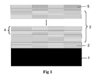
- Figure 1 shows a schematic drawing of one embodiment of the present invention showing a coating structure where the body 1 is coated with an innermost layer 2, the nanolaminated structure 3 comprising sequences 4 of alternating A and B layers according to any of the exemplary embodiments of the invention, and an outermost layer 5.
- said coating consists of an innermost single layer and/or multilayer 2 comprising, e.g., TiN, TiC, Ti(C,N) or (Ti,Al)N, preferably a single layer of (Ti,Al)N, followed by said nanolaminated structure (3) and optionally an outermost single layer and/or multilayer 5 comprising, e.g., TiN, TiC, Ti(C,N) or (Ti,Al)N, preferably a single layer of TiN, said coating having a total thickness between 1 ⁇ m and 20 ⁇ m, preferably between 1 ⁇ m and 15 ⁇ m and most preferably between 1 ⁇ m and 7 ⁇ m.
- an innermost single layer and/or multilayer 2 comprising, e.g., TiN, TiC, Ti(C,N) or (Ti,Al)N, preferably a single layer of (Ti,Al)N, followed by said nanolaminated structure (3) and optionally an outermost single layer and/or multilayer
- the deposition method for said nanolaminated structure is based on physical vapour deposition (PVD) techniques, preferably cathodic arc evaporation, using alloyed or composite cathodes in a reactive atmosphere containing N 2 , optionally with a carrier gas such as, e.g. Ar, at a total gas pressure between 1.0 Pa and 7.0 Pa, preferably between 1.5 Pa and 4.0 Pa, an evaporation current between 50 A and 200 A, a negative substrate bias between 0 V and 300 V, preferably between 10 V and 150 V, most preferably between 15 V and 100 V, and a deposition temperature between 200 °C and 800 °C, preferably between 300 °C and 600 °C.
- PVD physical vapour deposition
- the desired A layer and B layer compositions are obtained by selecting appropriate composition of the (Al,Me1) cathode/s, where Me1 is one or more of the elements Ti, Y, V, Nb, Mo, Si, Cr and W, and composition of the (Zr,Si,Me2) cathode/s, where Me2 is one or more of the elements Y, Ti, Nb, Ta, Cr, Mo, W and Al, respectively.
- the cathodes are mounted on opposing sides of the deposition chamber in order to obtain the nanolaminated structure by fixture rotation where the average individual layer thickness set by the evaporation current and the rotation speed of the fixture.
- the invention also relates to the use of cutting tool inserts according to the above for machining of stainless steel, super alloys and hardened steel at cutting speeds of 50 - 500 m/min, preferably 50 - 300 m/min, with an average feed of 0.08 - 0.5 mm/rev, preferably 0.1 - 0.4 mm/rev, depending on cutting speed and insert geometry.
- the present invention has been described with reference to a cutting tool insert but it is evident that it also can be applied to other metal cutting tools, e.g., drills and end mills.
- Cemented carbide cutting tool inserts with composition 94 wt% WC - 6 wt% Co were deposited by cathodic arc evaporation.
- the inserts were cleaned in ultrasonic baths of an alkali solution and alcohol.
- the system was evacuated to a pressure of less than 2.0x10 -3 Pa, after which the inserts were sputter cleaned with Ar ions.
- the coatings were deposited from alloy or composite cathodes with a composition according to Table 1 to yield the desired composition of Layer A and Layer B, respectively, in 99.995% pure N 2 atmosphere at a total pressure of 2-6 Pa, using a bias of -20 to -60 V and an evaporation current of 60-200 A at 450 °C.
- the cathodes were mounted on opposing sides of the deposition chamber in order to obtain the nanolaminated structure by fixture rotation.
- the average individual layer thickness was varied by altering the cathode current (60-200 A) and the rotation speed of the fixture (1-5 rpm).
- the total coating thickness was about 3 ⁇ m for all inserts as measured on the flank face.
- the average composition of the nanolaminated structure was estimated from measurements by energy dispersive x-ray spectroscopy (EDS) analysis area using a LEO Ultra 55 scanning electron microscope operated at 10 kV and equipped with a Thermo Noran EDS detector. The data were evaluated using the Noran System Six (NSS version 2) software.
- EDS energy dispersive x-ray spectroscopy
- Hardness data were estimated by the nanoindentation technique of the layers after mechanical polishing of the surface using a UMIS 2000 nanoindentation system with a Berkovich diamond tip with a maximum tip load of 25 mN.
- Table 1 Coating Description Cathode composition - layer A (metal at.%) Cathode composition - layer B (metal at.%) # LaverA / LayerB Ti Cr Al Me1 Zr Si Me2 Coatings according to embodiments of the invention 1 TiAlN / ZrSiN 33 67 97 3 2 TiAlN / ZrSiN 50 50 97 3 3 TiAlN / ZrSiN 60 40 97 3 4 TiAlN / ZrSiN 33 67 95 5 5 TiAlN / ZrSiN 50 50 95 5 6 TiAlN / ZrSiN 60 40 95 5 7 TiAlN / ZrSiN 33 67 90 10 8 TiAlN / ZrSiN 50 50 90 10 9 Ti
- Table 2 summarizes the results for the example coatings according to the embodiments of the invention and comparative coatings (single layers). Table 2.
- Coating Description Layer thickn. (nm) Layer A: (Al x1 Me1 100-x1 ) (metal at%) Layer B: (Zr 100-x2-z2 Si x2 Me2 z2 ) (metal at%) Average Composition (at%) # Layer A / Layer B A B x1 100-x1 100-x2-z2 x2 z2 Ti Cr Al Zr Si Me1 Me2 N Coatings according to embodiments of the invention 1 TiAlN / ZrSiN 6 8 64 36 97 3 7,7 13,7 27,6 0,9 50,1 2 TiAlN / ZrSiN 6 7 49 51 97 3 11,8 11,3 26,2 0,8 49,8 3 TiAlN / ZrSiN 7 6 38 62 97 3 16,4 10,0 21,9 0,7 51,0 4 TiAlN / ZrSiN 6
Landscapes
- Chemical & Material Sciences (AREA)
- Engineering & Computer Science (AREA)
- Mechanical Engineering (AREA)
- Chemical Kinetics & Catalysis (AREA)
- Materials Engineering (AREA)
- Metallurgy (AREA)
- Organic Chemistry (AREA)
- Cutting Tools, Boring Holders, And Turrets (AREA)
- Physical Vapour Deposition (AREA)
Abstract
Description
- The present invention relates to a cutting tool insert coated with a hard and wear resistant PVD, physical vapor deposition, coating comprising a nanolaminated structure based on alternating Zr-and Al-based nitride layers, respectively. The invention also relates to a method for coating the insert and the use thereof.
- TiN has been widely used as a hard and wear resistance layer on cutting tools. However, due to its relatively poor oxidation resistance at elevated temperatures, the focus has shifted towards more complex ternary and quaternary compounds, e.g., as in the (Ti,Al)N and (Ti,Si)N systems that show improved properties that enables greater cutting speeds, prolonged tool life and machining of harder materials in a wide range of metal cutting applications.
-
CN 101338411 discloses Zr-Si-N layers grown by co-sputtering of pure Zr and pure Si targets in a mixed argon and nitrogen discharge on substrates to a total thickness of 2 to 3 µm. -
EP 1736565 discloses a cutting tool insert, solid end mill, or drill, comprising a body and a coating composed of one or more layers of refractory compounds of which at least one layer comprises a cubic (Me,Si)X phase, where Me is one or more of the elements Ti, V, Cr, Zr, Nb, Mo, Hf, Ta and Al, and X is one or more of the elements N, C, O or B. -
US 7,056,602 discloses a cutting tool insert coated with a cubic structured (TiyAlxMe1-x-y)N based layer where Me is one of the elements: Zr, Hf, V, Nb, Ta, Cr, Mo, W or Si, and: x is between 0.50 and 0.80; the ratio, x/(x+y), is between 0.50 and 0.85; the sum of Ti and Al subscripts, x+y, is between 0.7 and 1.0. - Coating optimization has also been obtained by applying different concepts of multilayers as; alternating Ti and Al containing layers (
US 6,309,738 ), oxygen and non-oxygen containing layers (US 6,254,984 ), one of the layers stacked in the multilayer consists itself of a multilayer (US 6,077,596 ), alternating nitrogen content (US 5,330,853 ) or using one metastable compound (US 5,503,912 ) or as aperiodic multilayer (US 6,103,357 ). -
WO 2010140958 discloses a cutting tool insert coated with a polycrystalline nanolaminated structure of alternating layers A and B where layer A is (Ti,Al,Me1)N and Me1 is optionally one or more of the elements fromgroup group - Today industry continuously seeks solutions for economic and high productivity/feed-through manufacturing. To meet these demands there is a need for new materials with advanced properties to improve tool life during operation. Within the metal cutting tool industry, a major part of this effort is focused to improve the wear behavior of the cutting tools by designing the properties of the coating material used in the application. Typically, a high productivity/feed-through cutting process results in a dramatic increase of the tool temperature and hence a coating material with a high temperature wear resistance is essential.
- It is an object of the present invention to provide a coated cutting tool insert with improved performance in metal cutting applications at elevated temperatures.
- It is a further object of the present invention to provide a coated cutting tool insert with improved wear resistant properties.
- According to a first aspect of the invention the object is achieved by a cutting tool insert for machining by chip removal comprising a body of a hard alloy of cemented carbide, cermet, ceramics, cubic boron nitride based material or high speed steel, preferably cemented carbide and cermet, onto which a hard and wear resistant coating is deposited, wherein said coating comprises at least one polycrystalline nanolaminated structure comprising sequences of alternating A and B layers, where said layer A is (Alx1Me11-x1)Ny1 with 0.3 < x1 < 0.95, 0.9 < y1 < 1.1 and Me1 is one or more of the elements Ti, Y, V, Nb, Mo, Si, Cr and W, and said layer B is (Zr1-x2-z2Six2Me2z2)Ny2 with 0 < x2 < 0.30, 0.90 < y2 < 1.20, 0 ≤ z2 < 0.25 and Me2 is one or more of the elements Y, Ti, Nb, Ta, Cr, Mo, W and Al, the average individual thickness of A and B layers is between 1 nm and 50 nm, and the nanolaminated structure has a thickness between 0.5 µm and 15 µm.
- According to a second aspect of the invention the object is achieved by a method for making a hard and wear resistant coating by growing a nanolaminated structure comprising sequences of alternating A: (Al,Me1)N and B: (Zr,Si,Me2)N layers by PVD, preferably by cathodic arc evaporation, using fixture rotations and at least two opposing and different composite and/or alloyed cathodes for the A and B layers, respectively, where Me1 is one or more of the elements: Ti, Y, V, Nb, Mo, Si, Cr and W, and Me2 is one or more of the elements: Y, Ti, Nb, Ta, Cr, Mo, W and Al in a reactive atmosphere containing N2, optionally with a carrier gas, e.g. Ar, at a total gas pressure between 1.0 Pa and 7.0 Pa, preferably between 1.5 Pa and 4.0 Pa, an evaporation current between 50 A and 200 A, a negative substrate bias between 0 V and 300 V, preferably between 10 V and 150 V, most preferably between 15 V and 100 V, and a deposition temperature between 200 °C and 800 °C, preferably between 300 °C and 600 °C.
- It has been found that combining sequences of alternating (Zr,Si)- and Al-based nitride layers in a nanolaminated coating structure onto a cutting tool insert significantly improves the tool life due to increased wear resistance and edge integrity, especially in machining operations at elevated temperatures.
- Further embodiments of the invention are defined in the dependent claims.
- According to a third aspect of the invention the object is achieved by use of a cutting tool insert for machining by chip removal, specifically generating high temperatures, at cutting speeds of 50 - 400 m/min, 75 - 300 m/min, with an average feed, per tooth in the case of milling, of 0.08 - 0.5 mm, preferably 0.1 - 0.4 mm, depending on cutting speed and insert geometry.
-
-
Figure 1 is a schematic drawing of one embodiment of the present invention showing the coating structure as it would appear in a cross sectional scanning electron microscope (SEM) micrograph. - According to the present invention, there is provided a cutting tool insert for machining by chip removal comprising a
body 1 of a hard alloy of cemented carbide, cermet, ceramics, cubic boron nitride based material or high speed steel, preferably cemented carbide and cermet, onto which a hard and wear resistant coating is deposited comprising at least one polycrystalline nanolaminatedstructure 3 comprisingsequences 4 of alternating A and B layers with a thickness of the nanolaminated structure between 0.5 and 15 µm, preferably between 0.5 and 10 µm, most preferably between 0.5 and 5 µm. The nanolaminated structure has an overall columnar structure with average column width between 20 and 1000 nm, preferably between 20 and 500 nm, and estimated from measurements by, e.g., cross section transmission electron microscopy of a middle region of the nanolaminated structure, i.e., in a region within 30 to 70 % of the thickness in the growth direction, and said average column width is the average of at least ten adjacent columns. - Said layer A is (Alx1Me11-x1)Ny1, where 0.3 < x1 < 0.95, preferably 0.45 < x1 < 0.75, 0.9 < y1 < 1.1, preferably 0.96 < y1 < 1.04, and Me1 is one or more of the elements Ti, Y, V, Nb, Mo, Si, Cr and W, preferably one or more of the elements Ti, Cr, Si and Nb.
- Said layer B is (Zr1-x2-z2Six2Me2z2)Ny2 with 0 < x2 < 0.30, preferably 0 < x2 < 0.15, most preferably 0 < x2 < 0.085, 0.90 < y2 < 1.20, preferably 0.90 < y2 < 1.10, 0 ≤ z2 < 0.25, preferably 0 ≤ z2 < 0.15, most preferably 0 ≤ z2 < 0.10, and Me2 is one or more of the elements Y, Ti, Nb, Ta, Cr, Mo, W and Al, preferably one or more of the elements Ti, Ta and Cr, most preferably one or more of the elements Ta and Cr.
- Said A and B layers have an average individual layer thickness between 1 nm and 50 nm, preferably between 1 nm and 30 nm, most preferably between 2 nm and 20 nm, and is estimated from measurements by, e.g., cross sectional transmission electron microscopy in a middle region of the nanolaminated structure, i.e., in a region within 30 to 70 % of its thickness in the growth direction, and said average individual layer thickness is the average thickness of at least ten adjacent layers. Unintentional and small, aperiodic and/or periodic, thickness variation of layer A and B is common to the coating process due to, e.g., normal process variations, fixturing arrangement and rotation of the inserts during growth. In addition, the elemental composition of said thin (< 100 nm) A and B layers is estimated from measurements by, e.g., analytical transmission electron microscopy in scanning mode of operation (STEM) and EDS.
- Said nanolaminated structure comprises a phase mixture of cubic and hexagonal phases, preferably a cubic phase, as determined by X-ray diffraction.
- In one embodiment, said layer A is (Ti1-x1-z1Alx1Me1z1)Ny1, where 0.3 < x1 < 0.95, preferably 0.45 < x1 < 0.75, 0.9 < y1 < 1.1, preferably 0.96 < y1 < 1.04, and 0 ≤ z1 < 0.25, preferably 0 ≤ z1 < 0.15, and Me1 is one or more of the elements Y, V, Nb, Mo, Si, Cr and W, preferably one or more of the elements Cr, V, Si and Nb, most preferably one or more of the elements Cr, Nb and Si.
- In one embodiment, said layer A is (Cr1-x1-z1Alx1Me1z1)Ny1, where 0.3 < x1 < 0.95, preferably 0.45 < x1 < 0.75, 0.9 < y1 < 1.1, preferably 0.96 < y1 < 1.04, and 0 ≤ z1 ≤ 0.25, preferably 0 ≤ z1 < 0.15, and Me1 is one or more of the elements Ti, Y, V, Nb, Mo, Si and W, preferably one or more of the elements Ti, V, Si and Nb, most preferably one or more of the elements Ti, Nb and Si.
- The elemental composition of said A and B layers, i.e., x1, y1, z1, x2, y2 and z2, is estimated from measurements by, e.g., EDS or WDS techniques on the corresponding thick (> 2µm) monolayers. The composition of said monolayers is, within the accuracy for the measurements, essentially constant all through the monolayer thickness with a variation less than 10%, including the influence of normal process variations such as, e.g., rotation of the inserts during growth. In one embodiment z1 = 0.
- In one embodiment z2 = 0.
- In one embodiment z1 = z2 = 0.
- In one embodiment Me1 is one or more of the elements Ti, Cr, Si and Nb.
- In one embodiment Me2 is one or more of the elements Ti, Ta and Cr.
- Said coating has a nanohardness >20 GPa, preferably between 25 GPa and 40 GPa, most preferably between 30 GPa and 40 GPa, as measured by nanoindentation experiments.
- It is evident that said nanolaminated structure can be part of a complex coating design and used, e.g., as an inner, middle and/or outer nanolaminated structure of said complex coating.
-
Figure 1 shows a schematic drawing of one embodiment of the present invention showing a coating structure where thebody 1 is coated with aninnermost layer 2, thenanolaminated structure 3 comprisingsequences 4 of alternating A and B layers according to any of the exemplary embodiments of the invention, and anoutermost layer 5. - In one embodiment, said coating consists of an innermost single layer and/or
multilayer 2 comprising, e.g., TiN, TiC, Ti(C,N) or (Ti,Al)N, preferably a single layer of (Ti,Al)N, followed by said nanolaminated structure (3) and optionally an outermost single layer and/ormultilayer 5 comprising, e.g., TiN, TiC, Ti(C,N) or (Ti,Al)N, preferably a single layer of TiN, said coating having a total thickness between 1 µm and 20 µm, preferably between 1 µm and 15 µm and most preferably between 1 µm and 7 µm. - The deposition method for said nanolaminated structure is based on physical vapour deposition (PVD) techniques, preferably cathodic arc evaporation, using alloyed or composite cathodes in a reactive atmosphere containing N2, optionally with a carrier gas such as, e.g. Ar, at a total gas pressure between 1.0 Pa and 7.0 Pa, preferably between 1.5 Pa and 4.0 Pa, an evaporation current between 50 A and 200 A, a negative substrate bias between 0 V and 300 V, preferably between 10 V and 150 V, most preferably between 15 V and 100 V, and a deposition temperature between 200 °C and 800 °C, preferably between 300 °C and 600 °C. The desired A layer and B layer compositions are obtained by selecting appropriate composition of the (Al,Me1) cathode/s, where Me1 is one or more of the elements Ti, Y, V, Nb, Mo, Si, Cr and W, and composition of the (Zr,Si,Me2) cathode/s, where Me2 is one or more of the elements Y, Ti, Nb, Ta, Cr, Mo, W and Al, respectively. The cathodes are mounted on opposing sides of the deposition chamber in order to obtain the nanolaminated structure by fixture rotation where the average individual layer thickness set by the evaporation current and the rotation speed of the fixture.
- The invention also relates to the use of cutting tool inserts according to the above for machining of stainless steel, super alloys and hardened steel at cutting speeds of 50 - 500 m/min, preferably 50 - 300 m/min, with an average feed of 0.08 - 0.5 mm/rev, preferably 0.1 - 0.4 mm/rev, depending on cutting speed and insert geometry.
- The present invention has been described with reference to a cutting tool insert but it is evident that it also can be applied to other metal cutting tools, e.g., drills and end mills.
- Cemented carbide cutting tool inserts with composition 94 wt% WC - 6 wt% Co were deposited by cathodic arc evaporation.
- Before deposition, the inserts were cleaned in ultrasonic baths of an alkali solution and alcohol. The system was evacuated to a pressure of less than 2.0x10⁻³ Pa, after which the inserts were sputter cleaned with Ar ions. The coatings were deposited from alloy or composite cathodes with a composition according to Table 1 to yield the desired composition of Layer A and Layer B, respectively, in 99.995% pure N2 atmosphere at a total pressure of 2-6 Pa, using a bias of -20 to -60 V and an evaporation current of 60-200 A at 450 °C. The cathodes were mounted on opposing sides of the deposition chamber in order to obtain the nanolaminated structure by fixture rotation. The average individual layer thickness was varied by altering the cathode current (60-200 A) and the rotation speed of the fixture (1-5 rpm). The total coating thickness was about 3 µm for all inserts as measured on the flank face.
- The average composition of the nanolaminated structure was estimated from measurements by energy dispersive x-ray spectroscopy (EDS) analysis area using a LEO Ultra 55 scanning electron microscope operated at 10 kV and equipped with a Thermo Noran EDS detector. The data were evaluated using the Noran System Six (NSS version 2) software.
- Hardness data were estimated by the nanoindentation technique of the layers after mechanical polishing of the surface using a UMIS 2000 nanoindentation system with a Berkovich diamond tip with a maximum tip load of 25 mN.
Table 1. Coating Description Cathode composition - layer A (metal at.%) Cathode composition - layer B (metal at.%) # LaverA / LayerB Ti Cr Al Me1 Zr Si Me2 Coatings according to embodiments of the invention 1 TiAlN / ZrSiN 33 67 97 3 2 TiAlN / ZrSiN 50 50 97 3 3 TiAlN / ZrSiN 60 40 97 3 4 TiAlN / ZrSiN 33 67 95 5 5 TiAlN / ZrSiN 50 50 95 5 6 TiAlN / ZrSiN 60 40 95 5 7 TiAlN / ZrSiN 33 67 90 10 8 TiAlN / ZrSiN 50 50 90 10 9 TiAlN / ZrSiN 60 40 90 10 10 TiAlN / ZrSiN 33 67 95 5 11 TiAlN / ZrSiN 50 50 95 5 12 TiAlN / ZrSiN 33 67 95 5 13 TiAlN / ZrSiN 50 50 95 5 14 TiAlN / ZrSiN 33 67 95 5 15 TiAlN / ZrSiN 33 67 95 5 16 TiAlN / ZrSiN 33 67 95 5 17 CrAlN / ZrSiN 60 40 95 5 18 CrAlN / ZrSiN 45 55 95 5 19 CrAlN / ZrSiN 33 67 95 5 20 TiAlCrN / ZrSiN 30 60 10 95 5 21 TiAlSiN / ZrSiN 30 60 10 95 5 22 TiAINbN / ZrSiN 30 60 10 95 5 23 TiAlN / ZrSiCrN 40 60 85 5 10 24 TiAlN / ZrSiTaN 40 60 85 5 10 25 TiAlCrN / ZrSiCrN 30 60 10 85 5 10 Comparative 26 TiAlN 33 67 27 TiAlN 50 50 28 ZrSiN 95 5 29 ZrSiN 90 10 - Table 2 summarizes the results for the example coatings according to the embodiments of the invention and comparative coatings (single layers).
Table 2. Coating Description Layer thickn. (nm) Layer A: (Alx1 Me1100-x1) (metal at%) Layer B: (Zr100-x2-z2Six2Me2z2) (metal at%) Average Composition (at%) # Layer A / Layer B A B x1 100-x1 100-x2-z2 x2 z2 Ti Cr Al Zr Si Me1 Me2 N Coatings according to embodiments of the invention 1 TiAlN / ZrSiN 6 8 64 36 97 3 7,7 13,7 27,6 0,9 50,1 2 TiAlN / ZrSiN 6 7 49 51 97 3 11,8 11,3 26,2 0,8 49,8 3 TiAlN / ZrSiN 7 6 38 62 97 3 16,4 10,0 21,9 0,7 51,0 4 TiAlN / ZrSiN 6 8 64 36 96 4 7,5 13,3 26,5 1,1 51,6 5 TiAlN / ZrSiN 6 7 49 51 96 4 11,9 11,4 26,0 1,1 49,6 6 TiAlN / ZrSiN 7 6 38 62 96 4 16,4 10,0 21,7 0,9 51,0 7 TiAlN / ZrSiN 6 8 64 36 91 9 7,3 12,9 24,4 2,4 53,0 8 TiAlN / ZrSiN 6 7 49 51 91 9 11,1 10,7 23,1 2,3 52,8 9 TiAlN / ZrSiN 7 6 38 62 91 9 16,4 10,1 20,6 2,0 50,8 10 TiAlN / ZrSiN 3 3 64 36 96 4 8,8 15,7 23,5 1,0 51,0 11 TiAlN / ZrSiN 4 3 49 51 96 4 14,3 13,7 20,2 0,8 51,0 12 TiAlN / ZrSiN 12 10 64 36 96 4 9,6 17,1 21,4 0,9 51,0 13 TiAlN / ZrSiN 11 10 49 51 96 4 13,2 12,7 22,6 0,9 50,5 14 TiAlN / ZrSiN 5 15 64 36 96 4 4,5 8,0 35,8 1,5 50,3 15 TiAlN / ZrSiN 15 5 64 36 96 4 13,6 24,2 12,1 0,5 49,5 16 TiAlN / ZrSiN 25 25 64 36 96 4 8,8 15,7 23,5 1,0 51,0 17 CrAlN / ZrSiN 7 8 40 60 96 4 14,0 9,3 25,6 1,1 50,0 18 CrAlN / ZrSiN 7 8 55 45 96 4 10,5 12,8 25,6 1,1 50,0 19 CrAlN / ZrSiN 8 8 66 34 96 4 8,5 16,5 24,0 1,0 50,0 20 TiAlCrN / ZrSiN 9 12 62 38 96 4 6,2 12,8 26,5 1,1 1,7 51,6 21 TiAlSiN / ZrSiN 8 7 62 38 96 4 8,4 16,7 22,7 0,9 1,9 49,4 22 TiAlNbN / ZrSiN 5 6 62 38 96 4 6,9 14,2 26,4 1,1 1,8 49,6 23 TiAlN / ZrSiCrN 5 8 62 38 88 4 8 7,2 11,7 26,5 1,2 2,4 51,0 24 TiAlN / ZrSiTaN 5 6 62 38 89 4 7 8,3 13,6 23,5 1,1 1,8 51,7 25 TiAlCrN / ZrSiCrN 6 7 62 38 88 4 8 6.8 14,0 23.2 1,1 1,8 2,1 51,0 Comparative 26 TiAlN 18,6 31,0 50,4 27 TiAlN 24,5 24,9 50,6 28 ZrSiN 47,0 2,0 51,0 29 ZrSiN 42.8 4.2 53.0 -
Coatings 2, 4-6, 8, 16, 18-21 and 26-29 were tested under the following conditions:Geometry: CNMG120408-MF1 Application: Longitudinal turning Work piece material: AISI 316L Cutting speed: 300 m/min Feed: 0.15 mm/rev Depth of cut: 1.5 mm Tool life criteria: Flank wear (vb) > 0.3 mm - The results are presented in Table 3.
Table 3. Coating Crater wear resistance Flank wear resistance Life time (min) Coatings according to embodiments of the invention 2 Good/Medium Good 12 4 Good Good 14 5 Good Good/Medium 14 6 Good Good/Medium 14 8 Good/Medium Good/Medium 12 16 Medium Good 12 18 Good/Medium Good/Medium 12 19 Medium Good 12 20 Good Good/Medium 14 21 Good Medium 13 Comparative 26 Medium/Poor Good 12 27 Medium Good/Medium 10 28 Good Medium 8 29 Good Medium 10 - The cutting results presented in Table 3 clearly indicate that all coatings tested, containing a nanolaminated structure, perform well compared to the comparative coatings with an overall good wear resistance.
Coating 4 shows the best cutting results.
Claims (14)
- Cutting tool insert for machining by chip removal comprising a body (1) of a hard alloy of cemented carbide, cermet, ceramics, cubic boron nitride based material or high speed steel, onto which a hard and wear resistant PVD coating is deposited characterised in that said coating comprises at least one polycrystalline nanolaminated structure (3) comprising sequences (4) of alternating A and B layers, where said layer A is (Alx1Me11-x1)Ny1 with 0.3 < x1 < 0.95, 0.9 < y1 < 1.1 and Me1 is one or more of the elements Ti, Y, V, Nb, Mo, Si, Cr and W, and said layer B is (Zr1-x2-z2Six2Me2z2)Ny2 with 0 < x2 < 0.30, 0.90 < y2 < 1.20, 0 ≤ z2 < 0.25 and Me2 is one or more of the elements Y, Ti, Nb, Ta, Cr, Mo, W and Al, the average individual thickness of A and B layers is between 1 nm and 50 nm, and the nanolaminated structure has a thickness between 0.5 µm and 15 µm.
- Cutting tool insert according to claim 1, wherein said layer A is (Ti1-x1-z1Alx1Me1z1)Ny1, where 0.3 < x1 < 0.95, 0.9 < y1 < 1.1, 0 ≤ z1 < 0.25 and Me1 is one or more of the elements Y, V, Nb, Mo, Si, Cr and W.
- Cutting tool insert according to claim 1, wherein said layer A is (Cr1-x1-z1Alx1Me1z1)Ny1, where 0.3 < x1 < 0.95, 0.9 < y1 < 1.1, 0 ≤ z1 < 0.25 and Me1 is one or more of the elements Ti, Y, V, Nb, Mo, Si and W.
- Cutting tool insert according to any of the preceding claims, wherein 0.45 < x1 < 0.75.
- Cutting tool insert according to any of the preceding claims, wherein 0.96 < y1 < 1.04.
- Cutting tool insert according to any of the preceding claims, wherein 0 < x2 < 0.15.
- Cutting tool insert according to any of the preceding claims, wherein 0.90 < y2 < 1.10.
- Cutting tool insert according to any of claims 2-7, wherein 0 ≤ z1 = z2 < 0.15.
- Cutting tool insert according to any of claims 2-7, wherein z1 = 0.
- Cutting tool insert according to any of the preceding claims, wherein z2 = 0.
- Cutting tool insert according to any of the preceding claims, wherein said nanolaminated structure comprises a phase mixture of cubic and hexagonal phases, preferably a cubic phase.
- Cutting tool insert according to any of the preceding claims, wherein said coating consists of an innermost single layer and/or multilayer (2) comprising, e.g., TiN, TiC, Ti(C,N) or (Ti,Al)N, preferably a single layer of (Ti,Al)N, followed by said nanolaminated structure (3) and optionally an outer single layer and/or multilayer (5) comprising, e.g., TiN, TiC, Ti(C,N) or (Ti,Al)N, preferably a single layer of TiN, said coating having a total thickness between 1 µm and 20 µm.
- Method of making a hard and wear resistant nanolaminated coating structure characterised in growing sequences of alternating A: (Al,Me1)N and B:(Zr,Si,Me2)N layers by PVD, preferably by cathodic arc evaporation, using fixture rotation and at least two opposing and different composite and/or alloyed cathodes for the A and B layers, respectively, where Me1 is one or more of the elements: Ti, Y, V, Nb, Mo, Si, Cr and W, and Me2 is one or more of the elements: Y, Ti, Nb, Ta, Cr, Mo, W and Al in a reactive atmosphere containing N2, optionally with a carrier gas, e.g. Ar, at a total gas pressure between 1.0 Pa and 7.0 Pa, preferably between 1.5 Pa and 4.0 Pa, an evaporation current between 50 A and 200 A, a negative substrate bias between 0 V and 300 V, preferably between 10 V and 150 V, most preferably between 15 V and 100 V, and a deposition temperature between 200 °C and 800 °C, preferably between 300 °C and 600 °C.
- Use of a cutting tool inserts according to any of claims 1 - 12 for machining by chip removal, specifically generating high temperatures, at cutting speeds of 50 - 400 m/min, preferably 75 - 300 m/min, with an average feed, per tooth in the case of milling, of 0.08 - 0.5 mm, preferably 0.1 - 0.4 mm, depending on cutting speed and insert geometry.
Priority Applications (6)
| Application Number | Priority Date | Filing Date | Title |
|---|---|---|---|
| EP12158414.8A EP2636764B1 (en) | 2012-03-07 | 2012-03-07 | Nanolaminated coated cutting tool |
| US14/382,854 US9388487B2 (en) | 2012-03-07 | 2013-03-06 | Nanolaminated coated cutting tool |
| RU2014140341A RU2014140341A (en) | 2012-03-07 | 2013-03-06 | NANOLAMINAR COATING CUTTING TOOL |
| PCT/EP2013/054514 WO2013131961A1 (en) | 2012-03-07 | 2013-03-06 | Nanolaminated coated cutting tool |
| CN201380012427.7A CN104204275B (en) | 2012-03-07 | 2013-03-06 | Nanolaminated Coated Cutting Tools |
| KR1020147025167A KR20140133561A (en) | 2012-03-07 | 2013-03-06 | Nanolaminated coated cutting tool |
Applications Claiming Priority (1)
| Application Number | Priority Date | Filing Date | Title |
|---|---|---|---|
| EP12158414.8A EP2636764B1 (en) | 2012-03-07 | 2012-03-07 | Nanolaminated coated cutting tool |
Publications (2)
| Publication Number | Publication Date |
|---|---|
| EP2636764A1 true EP2636764A1 (en) | 2013-09-11 |
| EP2636764B1 EP2636764B1 (en) | 2014-07-09 |
Family
ID=47827218
Family Applications (1)
| Application Number | Title | Priority Date | Filing Date |
|---|---|---|---|
| EP12158414.8A Not-in-force EP2636764B1 (en) | 2012-03-07 | 2012-03-07 | Nanolaminated coated cutting tool |
Country Status (6)
| Country | Link |
|---|---|
| US (1) | US9388487B2 (en) |
| EP (1) | EP2636764B1 (en) |
| KR (1) | KR20140133561A (en) |
| CN (1) | CN104204275B (en) |
| RU (1) | RU2014140341A (en) |
| WO (1) | WO2013131961A1 (en) |
Cited By (5)
| Publication number | Priority date | Publication date | Assignee | Title |
|---|---|---|---|---|
| GB2519840A (en) * | 2013-08-16 | 2015-05-06 | Kennametal Inc | Low stress hard coatings and applications thereof |
| CN104630706A (en) * | 2015-01-21 | 2015-05-20 | 北京科技大学 | High-property optothermal transformation multiple-element alloy nitride film and preparation method thereof |
| US9168664B2 (en) | 2013-08-16 | 2015-10-27 | Kennametal Inc. | Low stress hard coatings and applications thereof |
| CN111910159A (en) * | 2020-08-10 | 2020-11-10 | 株洲华锐精密工具股份有限公司 | Nanocrystalline amorphous composite coating, preparation method thereof and cutter |
| CN114072541A (en) * | 2019-05-17 | 2022-02-18 | 奥钢联艾弗勒涂层有限公司 | Method for manufacturing improved cold forming tool for high strength and ultra high strength steels and cold forming tool |
Families Citing this family (25)
| Publication number | Priority date | Publication date | Assignee | Title |
|---|---|---|---|---|
| CO6700142A1 (en) * | 2013-06-07 | 2013-06-28 | Univ Del Valle | Biocompatible coating multilayer-thin film type as surface treatment of biomedical substrates and manufacturing process |
| CN104878359B (en) * | 2015-06-12 | 2018-07-06 | 浙江嵘润机械有限公司 | High rigidity and high-wearing feature TiAlN/ZrSiN nanostructured protective coatings and preparation method thereof |
| CN108368601B (en) * | 2015-12-22 | 2020-10-30 | 山特维克知识产权股份有限公司 | Coated cutting tool and method |
| CN105543780B (en) * | 2015-12-28 | 2018-02-09 | 富耐克超硬材料股份有限公司 | Superhard cutter surface recombination hard coat and preparation method thereof |
| CN105624618B (en) * | 2016-02-11 | 2018-01-19 | 广东工业大学 | TiAlSiZrN base composite coatings, the gradient ultra-fine cemented carbide cutter with the composite coating and preparation method thereof |
| WO2017170536A1 (en) * | 2016-03-30 | 2017-10-05 | 三菱日立ツール株式会社 | Coated cutting tool |
| US11059105B2 (en) * | 2016-11-29 | 2021-07-13 | Sumitomo Electric Hardmetal Corp. | Surface-coated cutting tool |
| JP6635347B2 (en) * | 2017-06-27 | 2020-01-22 | 株式会社タンガロイ | Coated cutting tool |
| JP7217740B2 (en) * | 2017-08-31 | 2023-02-03 | ヴァルター アーゲー | Wear-resistant PVD tool coating with TiAlN nanolayer film |
| WO2019171648A1 (en) * | 2018-03-07 | 2019-09-12 | 住友電工ハードメタル株式会社 | Surface-coated cutting tool and method for producing same |
| US11370033B2 (en) * | 2018-03-07 | 2022-06-28 | Sumitomo Electric Hardmetal Corp. | Surface coated cutting tool and method for manufacturing the same |
| WO2020026390A1 (en) * | 2018-08-01 | 2020-02-06 | オーエスジー株式会社 | Hard coating and member coated with hard coating |
| US11447873B2 (en) * | 2018-08-01 | 2022-09-20 | Osg Corporation | Hard coating and hard-coating-covered member |
| EP3943222A4 (en) * | 2019-03-22 | 2022-08-03 | MOLDINO Tool Engineering, Ltd. | Coated cutting tool |
| WO2021106440A1 (en) * | 2019-11-27 | 2021-06-03 | 株式会社Moldino | Coated cutting tool |
| DE112021001912T5 (en) * | 2020-03-27 | 2023-01-12 | Kyocera Corporation | COATED TOOL AND CUTTING TOOL |
| DE112021001914T5 (en) * | 2020-03-27 | 2023-01-05 | Kyocera Corporation | COATED TOOL AND CUTTING TOOL |
| CN111910172B (en) * | 2020-07-24 | 2022-10-18 | 株洲钻石切削刀具股份有限公司 | Composite coating PCBN cutting tool and preparation method thereof |
| JP7808110B2 (en) * | 2020-11-30 | 2026-01-28 | エリコン・サーフェス・ソリューションズ・アクチェンゲゼルシャフト,プフェフィコーン | Molybdenum nitride based multilayer coatings for wear and friction reduction |
| CN114686822B (en) * | 2022-04-07 | 2023-10-20 | 株洲华锐精密工具股份有限公司 | M (AlTiNbN/AlTiON) +AlTiCON multilayer composite coating for cutting and preparation method thereof |
| US12138692B2 (en) * | 2022-09-22 | 2024-11-12 | Sumitomo Electric Industries, Ltd. | Cutting tool |
| CN116180023B (en) * | 2023-02-24 | 2025-06-13 | 厦门钨业股份有限公司 | Nano multilayer structure coating and its preparation method and application |
| JPWO2024185311A1 (en) * | 2023-03-06 | 2024-09-12 | ||
| CN116926470B (en) * | 2023-07-03 | 2025-08-29 | 岭南师范学院 | TiBCrYN coating for rotary tillage tool and preparation method thereof |
| CN116949399B (en) * | 2023-07-03 | 2025-10-31 | 岭南师范学院 | Coating structure for rotary tillage cutter and preparation method thereof |
Citations (14)
| Publication number | Priority date | Publication date | Assignee | Title |
|---|---|---|---|---|
| US5330853A (en) | 1991-03-16 | 1994-07-19 | Leybold Ag | Multilayer Ti-Al-N coating for tools |
| US5503912A (en) | 1992-10-12 | 1996-04-02 | Sumitomo Electric Industries, Ltd. | Ultra-thin film laminate |
| US6077596A (en) | 1997-06-19 | 2000-06-20 | Sumitomo Electric Industries, Ltd. | Coated hard tool having multi-layer coating |
| US6103357A (en) | 1997-04-18 | 2000-08-15 | Sandvik Ab | Multilayered coated cutting tool |
| US6254984B1 (en) | 1998-03-16 | 2001-07-03 | Hitachi Tool Engineering, Ltd. | Members with multi-layer coatings |
| US6309738B1 (en) | 1998-02-04 | 2001-10-30 | Osg Corporation | Hard multilayer coated tool having increased toughness |
| JP2005028476A (en) * | 2003-07-09 | 2005-02-03 | Mitsubishi Materials Corp | Surface coated cemented carbide cutting tool with excellent chipping resistance with hard coating layer under high speed heavy cutting conditions |
| US7056602B2 (en) | 2002-09-04 | 2006-06-06 | Seco Tools Ab | Precipitation hardened wear resistant coating |
| EP1736565A1 (en) | 2005-06-22 | 2006-12-27 | Seco Tools Ab | Composite coatings for finishing of hardened steels |
| JP2008302474A (en) * | 2007-06-07 | 2008-12-18 | Sumitomo Electric Hardmetal Corp | Surface coated cutting tool |
| CN101338411A (en) | 2008-08-15 | 2009-01-07 | 江苏科技大学 | Zr-Si-N hard composite coating and its preparation method |
| WO2010140958A1 (en) | 2009-06-01 | 2010-12-09 | Seco Tools Ab | Nanolaminated coated cutting tool |
| WO2010140959A1 (en) * | 2009-06-01 | 2010-12-09 | Seco Tools Ab | Nanolaminated coated cutting tool |
| DE102010039035A1 (en) * | 2010-08-06 | 2012-02-09 | Walter Ag | Cutting tool with multilayer coating |
Family Cites Families (4)
| Publication number | Priority date | Publication date | Assignee | Title |
|---|---|---|---|---|
| US5700551A (en) * | 1994-09-16 | 1997-12-23 | Sumitomo Electric Industries, Ltd. | Layered film made of ultrafine particles and a hard composite material for tools possessing the film |
| EP1914331B1 (en) * | 2006-10-18 | 2019-07-24 | Sandvik Intellectual Property AB | Coated cutting tool |
| EP2098611B1 (en) * | 2008-03-07 | 2013-02-13 | Seco Tools AB | Layered coated cutting tool |
| EP2300636B1 (en) * | 2008-06-13 | 2014-07-23 | Seco Tools AB | Coated cutting tool for metal cutting applications generating high temperatures |
-
2012
- 2012-03-07 EP EP12158414.8A patent/EP2636764B1/en not_active Not-in-force
-
2013
- 2013-03-06 RU RU2014140341A patent/RU2014140341A/en not_active Application Discontinuation
- 2013-03-06 US US14/382,854 patent/US9388487B2/en not_active Expired - Fee Related
- 2013-03-06 WO PCT/EP2013/054514 patent/WO2013131961A1/en not_active Ceased
- 2013-03-06 CN CN201380012427.7A patent/CN104204275B/en not_active Expired - Fee Related
- 2013-03-06 KR KR1020147025167A patent/KR20140133561A/en not_active Withdrawn
Patent Citations (14)
| Publication number | Priority date | Publication date | Assignee | Title |
|---|---|---|---|---|
| US5330853A (en) | 1991-03-16 | 1994-07-19 | Leybold Ag | Multilayer Ti-Al-N coating for tools |
| US5503912A (en) | 1992-10-12 | 1996-04-02 | Sumitomo Electric Industries, Ltd. | Ultra-thin film laminate |
| US6103357A (en) | 1997-04-18 | 2000-08-15 | Sandvik Ab | Multilayered coated cutting tool |
| US6077596A (en) | 1997-06-19 | 2000-06-20 | Sumitomo Electric Industries, Ltd. | Coated hard tool having multi-layer coating |
| US6309738B1 (en) | 1998-02-04 | 2001-10-30 | Osg Corporation | Hard multilayer coated tool having increased toughness |
| US6254984B1 (en) | 1998-03-16 | 2001-07-03 | Hitachi Tool Engineering, Ltd. | Members with multi-layer coatings |
| US7056602B2 (en) | 2002-09-04 | 2006-06-06 | Seco Tools Ab | Precipitation hardened wear resistant coating |
| JP2005028476A (en) * | 2003-07-09 | 2005-02-03 | Mitsubishi Materials Corp | Surface coated cemented carbide cutting tool with excellent chipping resistance with hard coating layer under high speed heavy cutting conditions |
| EP1736565A1 (en) | 2005-06-22 | 2006-12-27 | Seco Tools Ab | Composite coatings for finishing of hardened steels |
| JP2008302474A (en) * | 2007-06-07 | 2008-12-18 | Sumitomo Electric Hardmetal Corp | Surface coated cutting tool |
| CN101338411A (en) | 2008-08-15 | 2009-01-07 | 江苏科技大学 | Zr-Si-N hard composite coating and its preparation method |
| WO2010140958A1 (en) | 2009-06-01 | 2010-12-09 | Seco Tools Ab | Nanolaminated coated cutting tool |
| WO2010140959A1 (en) * | 2009-06-01 | 2010-12-09 | Seco Tools Ab | Nanolaminated coated cutting tool |
| DE102010039035A1 (en) * | 2010-08-06 | 2012-02-09 | Walter Ag | Cutting tool with multilayer coating |
Non-Patent Citations (2)
| Title |
|---|
| MARTIN P J ET AL: "Nanocomposite Ti-Si-N, Zr-Si-N, Ti-Al-Si-N, Ti-Al-V-Si-N thin film coatings deposited by vacuum arc deposition", SURFACE AND COATINGS TECHNOLOGY, ELSEVIER, AMSTERDAM, NL, vol. 200, no. 7, 21 December 2005 (2005-12-21), pages 2228 - 2235, XP027608588, ISSN: 0257-8972, [retrieved on 20051221] * |
| S. PALDEY, S.C. DEEVI: "Single layer and multilayer wear resistant coatings of (Ti,Al)N: a review", MATERIALS SCIENCE AND ENGINEERING, vol. A342, 1 January 2003 (2003-01-01), pages 58 - 79, XP002681141 * |
Cited By (9)
| Publication number | Priority date | Publication date | Assignee | Title |
|---|---|---|---|---|
| GB2519840A (en) * | 2013-08-16 | 2015-05-06 | Kennametal Inc | Low stress hard coatings and applications thereof |
| US9168664B2 (en) | 2013-08-16 | 2015-10-27 | Kennametal Inc. | Low stress hard coatings and applications thereof |
| US9896767B2 (en) | 2013-08-16 | 2018-02-20 | Kennametal Inc | Low stress hard coatings and applications thereof |
| CN104630706A (en) * | 2015-01-21 | 2015-05-20 | 北京科技大学 | High-property optothermal transformation multiple-element alloy nitride film and preparation method thereof |
| CN104630706B (en) * | 2015-01-21 | 2017-08-25 | 北京科技大学 | A kind of many primitive alloy nitride films of high-performance optical thermal transition and preparation method thereof |
| CN114072541A (en) * | 2019-05-17 | 2022-02-18 | 奥钢联艾弗勒涂层有限公司 | Method for manufacturing improved cold forming tool for high strength and ultra high strength steels and cold forming tool |
| CN114072541B (en) * | 2019-05-17 | 2023-12-19 | 奥钢联艾弗勒涂层有限公司 | Method of manufacturing improved cold forming tools for high strength and ultra high strength steels and cold forming tools |
| CN111910159A (en) * | 2020-08-10 | 2020-11-10 | 株洲华锐精密工具股份有限公司 | Nanocrystalline amorphous composite coating, preparation method thereof and cutter |
| CN111910159B (en) * | 2020-08-10 | 2022-08-30 | 株洲华锐精密工具股份有限公司 | Nanocrystalline amorphous composite coating, preparation method thereof and cutter |
Also Published As
| Publication number | Publication date |
|---|---|
| US9388487B2 (en) | 2016-07-12 |
| RU2014140341A (en) | 2016-04-27 |
| US20150023751A1 (en) | 2015-01-22 |
| KR20140133561A (en) | 2014-11-19 |
| CN104204275B (en) | 2016-07-06 |
| EP2636764B1 (en) | 2014-07-09 |
| CN104204275A (en) | 2014-12-10 |
| WO2013131961A1 (en) | 2013-09-12 |
Similar Documents
| Publication | Publication Date | Title |
|---|---|---|
| EP2636764B1 (en) | Nanolaminated coated cutting tool | |
| EP2098611B1 (en) | Layered coated cutting tool | |
| EP2438209B1 (en) | Nanolaminated coated cutting tool | |
| KR101831014B1 (en) | Coated cutting tool insert | |
| EP2446066B1 (en) | Nanolaminated coated cutting tool | |
| US9540722B2 (en) | Body with a metal based nitride layer and a method for coating the body | |
| JP6620482B2 (en) | Surface coated cutting tool with excellent chipping resistance | |
| EP3170919B1 (en) | Coated cutting tool | |
| US8741011B2 (en) | Coated cutting tool for metal cutting applications generating high temperatures | |
| EP2262924B1 (en) | Thermally stabilized (ti, si)n layer for cutting tool insert | |
| EP2300636B1 (en) | Coated cutting tool for metal cutting applications generating high temperatures | |
| US20070275268A1 (en) | Cutting tool made of surface-coated cubic boron nitride-based ultra-high-pressure sintered material | |
| US10023952B2 (en) | Coated cutting tool and a method for coating the cutting tool | |
| JP2014210333A (en) | Surface-coated cutting tool with hard coated layer exerting excellent chipping resistance | |
| EP3228726A1 (en) | Coated cutting tool | |
| JP2017221992A (en) | Surface coated cutting tool | |
| US20120009402A1 (en) | Coated cutting tool for metal cutting applications generating high temperatures | |
| JP2019118995A (en) | Surface-coated cutting tool | |
| EP3263736A1 (en) | A coated cutting tool and a method for coating the cutting tool | |
| JP7132548B2 (en) | surface coated cutting tools | |
| JP5321356B2 (en) | Surface coated cutting tool | |
| JP2019118997A (en) | Surface-coated cutting tool | |
| WO2025115120A1 (en) | Cutting tool |
Legal Events
| Date | Code | Title | Description |
|---|---|---|---|
| PUAI | Public reference made under article 153(3) epc to a published international application that has entered the european phase |
Free format text: ORIGINAL CODE: 0009012 |
|
| 17P | Request for examination filed |
Effective date: 20120307 |
|
| AK | Designated contracting states |
Kind code of ref document: A1 Designated state(s): AL AT BE BG CH CY CZ DE DK EE ES FI FR GB GR HR HU IE IS IT LI LT LU LV MC MK MT NL NO PL PT RO RS SE SI SK SM TR |
|
| AX | Request for extension of the european patent |
Extension state: BA ME |
|
| GRAP | Despatch of communication of intention to grant a patent |
Free format text: ORIGINAL CODE: EPIDOSNIGR1 |
|
| INTG | Intention to grant announced |
Effective date: 20140218 |
|
| RBV | Designated contracting states (corrected) |
Designated state(s): AL AT BE BG CH CY CZ DE DK EE ES FI FR GB GR HR HU IE IS IT LI LT LU LV MC MK MT NL NO PL PT RO RS SE SI SK SM TR |
|
| GRAS | Grant fee paid |
Free format text: ORIGINAL CODE: EPIDOSNIGR3 |
|
| GRAA | (expected) grant |
Free format text: ORIGINAL CODE: 0009210 |
|
| AK | Designated contracting states |
Kind code of ref document: B1 Designated state(s): AL AT BE BG CH CY CZ DE DK EE ES FI FR GB GR HR HU IE IS IT LI LT LU LV MC MK MT NL NO PL PT RO RS SE SI SK SM TR |
|
| REG | Reference to a national code |
Ref country code: GB Ref legal event code: FG4D |
|
| REG | Reference to a national code |
Ref country code: CH Ref legal event code: EP Ref country code: AT Ref legal event code: REF Ref document number: 676633 Country of ref document: AT Kind code of ref document: T Effective date: 20140715 |
|
| REG | Reference to a national code |
Ref country code: IE Ref legal event code: FG4D |
|
| REG | Reference to a national code |
Ref country code: DE Ref legal event code: R096 Ref document number: 602012002325 Country of ref document: DE Effective date: 20140828 |
|
| REG | Reference to a national code |
Ref country code: AT Ref legal event code: MK05 Ref document number: 676633 Country of ref document: AT Kind code of ref document: T Effective date: 20140709 |
|
| REG | Reference to a national code |
Ref country code: NL Ref legal event code: VDEP Effective date: 20140709 |
|
| REG | Reference to a national code |
Ref country code: LT Ref legal event code: MG4D |
|
| PG25 | Lapsed in a contracting state [announced via postgrant information from national office to epo] |
Ref country code: ES Free format text: LAPSE BECAUSE OF FAILURE TO SUBMIT A TRANSLATION OF THE DESCRIPTION OR TO PAY THE FEE WITHIN THE PRESCRIBED TIME-LIMIT Effective date: 20140709 Ref country code: FI Free format text: LAPSE BECAUSE OF FAILURE TO SUBMIT A TRANSLATION OF THE DESCRIPTION OR TO PAY THE FEE WITHIN THE PRESCRIBED TIME-LIMIT Effective date: 20140709 Ref country code: BG Free format text: LAPSE BECAUSE OF FAILURE TO SUBMIT A TRANSLATION OF THE DESCRIPTION OR TO PAY THE FEE WITHIN THE PRESCRIBED TIME-LIMIT Effective date: 20141009 Ref country code: GR Free format text: LAPSE BECAUSE OF FAILURE TO SUBMIT A TRANSLATION OF THE DESCRIPTION OR TO PAY THE FEE WITHIN THE PRESCRIBED TIME-LIMIT Effective date: 20141010 Ref country code: LT Free format text: LAPSE BECAUSE OF FAILURE TO SUBMIT A TRANSLATION OF THE DESCRIPTION OR TO PAY THE FEE WITHIN THE PRESCRIBED TIME-LIMIT Effective date: 20140709 Ref country code: SE Free format text: LAPSE BECAUSE OF FAILURE TO SUBMIT A TRANSLATION OF THE DESCRIPTION OR TO PAY THE FEE WITHIN THE PRESCRIBED TIME-LIMIT Effective date: 20140709 Ref country code: NO Free format text: LAPSE BECAUSE OF FAILURE TO SUBMIT A TRANSLATION OF THE DESCRIPTION OR TO PAY THE FEE WITHIN THE PRESCRIBED TIME-LIMIT Effective date: 20141009 Ref country code: PT Free format text: LAPSE BECAUSE OF FAILURE TO SUBMIT A TRANSLATION OF THE DESCRIPTION OR TO PAY THE FEE WITHIN THE PRESCRIBED TIME-LIMIT Effective date: 20141110 |
|
| PG25 | Lapsed in a contracting state [announced via postgrant information from national office to epo] |
Ref country code: AT Free format text: LAPSE BECAUSE OF FAILURE TO SUBMIT A TRANSLATION OF THE DESCRIPTION OR TO PAY THE FEE WITHIN THE PRESCRIBED TIME-LIMIT Effective date: 20140709 Ref country code: LV Free format text: LAPSE BECAUSE OF FAILURE TO SUBMIT A TRANSLATION OF THE DESCRIPTION OR TO PAY THE FEE WITHIN THE PRESCRIBED TIME-LIMIT Effective date: 20140709 Ref country code: HR Free format text: LAPSE BECAUSE OF FAILURE TO SUBMIT A TRANSLATION OF THE DESCRIPTION OR TO PAY THE FEE WITHIN THE PRESCRIBED TIME-LIMIT Effective date: 20140709 Ref country code: CY Free format text: LAPSE BECAUSE OF FAILURE TO SUBMIT A TRANSLATION OF THE DESCRIPTION OR TO PAY THE FEE WITHIN THE PRESCRIBED TIME-LIMIT Effective date: 20140709 Ref country code: PL Free format text: LAPSE BECAUSE OF FAILURE TO SUBMIT A TRANSLATION OF THE DESCRIPTION OR TO PAY THE FEE WITHIN THE PRESCRIBED TIME-LIMIT Effective date: 20140709 Ref country code: NL Free format text: LAPSE BECAUSE OF FAILURE TO SUBMIT A TRANSLATION OF THE DESCRIPTION OR TO PAY THE FEE WITHIN THE PRESCRIBED TIME-LIMIT Effective date: 20140709 Ref country code: IS Free format text: LAPSE BECAUSE OF FAILURE TO SUBMIT A TRANSLATION OF THE DESCRIPTION OR TO PAY THE FEE WITHIN THE PRESCRIBED TIME-LIMIT Effective date: 20141109 Ref country code: RS Free format text: LAPSE BECAUSE OF FAILURE TO SUBMIT A TRANSLATION OF THE DESCRIPTION OR TO PAY THE FEE WITHIN THE PRESCRIBED TIME-LIMIT Effective date: 20140709 |
|
| REG | Reference to a national code |
Ref country code: DE Ref legal event code: R097 Ref document number: 602012002325 Country of ref document: DE |
|
| PG25 | Lapsed in a contracting state [announced via postgrant information from national office to epo] |
Ref country code: CZ Free format text: LAPSE BECAUSE OF FAILURE TO SUBMIT A TRANSLATION OF THE DESCRIPTION OR TO PAY THE FEE WITHIN THE PRESCRIBED TIME-LIMIT Effective date: 20140709 Ref country code: EE Free format text: LAPSE BECAUSE OF FAILURE TO SUBMIT A TRANSLATION OF THE DESCRIPTION OR TO PAY THE FEE WITHIN THE PRESCRIBED TIME-LIMIT Effective date: 20140709 Ref country code: DK Free format text: LAPSE BECAUSE OF FAILURE TO SUBMIT A TRANSLATION OF THE DESCRIPTION OR TO PAY THE FEE WITHIN THE PRESCRIBED TIME-LIMIT Effective date: 20140709 Ref country code: SK Free format text: LAPSE BECAUSE OF FAILURE TO SUBMIT A TRANSLATION OF THE DESCRIPTION OR TO PAY THE FEE WITHIN THE PRESCRIBED TIME-LIMIT Effective date: 20140709 |
|
| PLBE | No opposition filed within time limit |
Free format text: ORIGINAL CODE: 0009261 |
|
| STAA | Information on the status of an ep patent application or granted ep patent |
Free format text: STATUS: NO OPPOSITION FILED WITHIN TIME LIMIT |
|
| 26N | No opposition filed |
Effective date: 20150410 |
|
| PG25 | Lapsed in a contracting state [announced via postgrant information from national office to epo] |
Ref country code: LU Free format text: LAPSE BECAUSE OF FAILURE TO SUBMIT A TRANSLATION OF THE DESCRIPTION OR TO PAY THE FEE WITHIN THE PRESCRIBED TIME-LIMIT Effective date: 20150307 Ref country code: MC Free format text: LAPSE BECAUSE OF FAILURE TO SUBMIT A TRANSLATION OF THE DESCRIPTION OR TO PAY THE FEE WITHIN THE PRESCRIBED TIME-LIMIT Effective date: 20140709 |
|
| REG | Reference to a national code |
Ref country code: CH Ref legal event code: PL |
|
| PG25 | Lapsed in a contracting state [announced via postgrant information from national office to epo] |
Ref country code: SI Free format text: LAPSE BECAUSE OF FAILURE TO SUBMIT A TRANSLATION OF THE DESCRIPTION OR TO PAY THE FEE WITHIN THE PRESCRIBED TIME-LIMIT Effective date: 20140709 |
|
| REG | Reference to a national code |
Ref country code: IE Ref legal event code: MM4A |
|
| PG25 | Lapsed in a contracting state [announced via postgrant information from national office to epo] |
Ref country code: CH Free format text: LAPSE BECAUSE OF NON-PAYMENT OF DUE FEES Effective date: 20150331 Ref country code: IE Free format text: LAPSE BECAUSE OF NON-PAYMENT OF DUE FEES Effective date: 20150307 Ref country code: LI Free format text: LAPSE BECAUSE OF NON-PAYMENT OF DUE FEES Effective date: 20150331 |
|
| REG | Reference to a national code |
Ref country code: FR Ref legal event code: PLFP Year of fee payment: 5 |
|
| PG25 | Lapsed in a contracting state [announced via postgrant information from national office to epo] |
Ref country code: BE Free format text: LAPSE BECAUSE OF FAILURE TO SUBMIT A TRANSLATION OF THE DESCRIPTION OR TO PAY THE FEE WITHIN THE PRESCRIBED TIME-LIMIT Effective date: 20140709 |
|
| PG25 | Lapsed in a contracting state [announced via postgrant information from national office to epo] |
Ref country code: MT Free format text: LAPSE BECAUSE OF FAILURE TO SUBMIT A TRANSLATION OF THE DESCRIPTION OR TO PAY THE FEE WITHIN THE PRESCRIBED TIME-LIMIT Effective date: 20140709 |
|
| REG | Reference to a national code |
Ref country code: FR Ref legal event code: PLFP Year of fee payment: 6 |
|
| PGFP | Annual fee paid to national office [announced via postgrant information from national office to epo] |
Ref country code: FR Payment date: 20170213 Year of fee payment: 6 Ref country code: DE Payment date: 20170228 Year of fee payment: 6 |
|
| PG25 | Lapsed in a contracting state [announced via postgrant information from national office to epo] |
Ref country code: SM Free format text: LAPSE BECAUSE OF FAILURE TO SUBMIT A TRANSLATION OF THE DESCRIPTION OR TO PAY THE FEE WITHIN THE PRESCRIBED TIME-LIMIT Effective date: 20140709 Ref country code: HU Free format text: LAPSE BECAUSE OF FAILURE TO SUBMIT A TRANSLATION OF THE DESCRIPTION OR TO PAY THE FEE WITHIN THE PRESCRIBED TIME-LIMIT; INVALID AB INITIO Effective date: 20120307 Ref country code: RO Free format text: LAPSE BECAUSE OF FAILURE TO SUBMIT A TRANSLATION OF THE DESCRIPTION OR TO PAY THE FEE WITHIN THE PRESCRIBED TIME-LIMIT Effective date: 20140709 |
|
| PGFP | Annual fee paid to national office [announced via postgrant information from national office to epo] |
Ref country code: GB Payment date: 20170301 Year of fee payment: 6 |
|
| PGFP | Annual fee paid to national office [announced via postgrant information from national office to epo] |
Ref country code: IT Payment date: 20170320 Year of fee payment: 6 |
|
| PG25 | Lapsed in a contracting state [announced via postgrant information from national office to epo] |
Ref country code: TR Free format text: LAPSE BECAUSE OF FAILURE TO SUBMIT A TRANSLATION OF THE DESCRIPTION OR TO PAY THE FEE WITHIN THE PRESCRIBED TIME-LIMIT Effective date: 20140709 |
|
| PG25 | Lapsed in a contracting state [announced via postgrant information from national office to epo] |
Ref country code: MK Free format text: LAPSE BECAUSE OF FAILURE TO SUBMIT A TRANSLATION OF THE DESCRIPTION OR TO PAY THE FEE WITHIN THE PRESCRIBED TIME-LIMIT Effective date: 20140709 |
|
| REG | Reference to a national code |
Ref country code: DE Ref legal event code: R119 Ref document number: 602012002325 Country of ref document: DE |
|
| PG25 | Lapsed in a contracting state [announced via postgrant information from national office to epo] |
Ref country code: AL Free format text: LAPSE BECAUSE OF FAILURE TO SUBMIT A TRANSLATION OF THE DESCRIPTION OR TO PAY THE FEE WITHIN THE PRESCRIBED TIME-LIMIT Effective date: 20140709 |
|
| GBPC | Gb: european patent ceased through non-payment of renewal fee |
Effective date: 20180307 |
|
| PG25 | Lapsed in a contracting state [announced via postgrant information from national office to epo] |
Ref country code: DE Free format text: LAPSE BECAUSE OF NON-PAYMENT OF DUE FEES Effective date: 20181002 |
|
| PG25 | Lapsed in a contracting state [announced via postgrant information from national office to epo] |
Ref country code: GB Free format text: LAPSE BECAUSE OF NON-PAYMENT OF DUE FEES Effective date: 20180307 Ref country code: IT Free format text: LAPSE BECAUSE OF NON-PAYMENT OF DUE FEES Effective date: 20180307 |
|
| PG25 | Lapsed in a contracting state [announced via postgrant information from national office to epo] |
Ref country code: FR Free format text: LAPSE BECAUSE OF NON-PAYMENT OF DUE FEES Effective date: 20180331 |