EP2633232B1 - Lighting assembly - Google Patents
Lighting assembly Download PDFInfo
- Publication number
- EP2633232B1 EP2633232B1 EP11782077.9A EP11782077A EP2633232B1 EP 2633232 B1 EP2633232 B1 EP 2633232B1 EP 11782077 A EP11782077 A EP 11782077A EP 2633232 B1 EP2633232 B1 EP 2633232B1
- Authority
- EP
- European Patent Office
- Prior art keywords
- assembly
- board
- casing
- boards
- pins
- Prior art date
- Legal status (The legal status is an assumption and is not a legal conclusion. Google has not performed a legal analysis and makes no representation as to the accuracy of the status listed.)
- Not-in-force
Links
- 230000005855 radiation Effects 0.000 claims description 15
- 230000015572 biosynthetic process Effects 0.000 claims description 8
- 238000005755 formation reaction Methods 0.000 claims description 8
- 230000002093 peripheral effect Effects 0.000 claims description 2
- 238000005516 engineering process Methods 0.000 description 6
- 238000000034 method Methods 0.000 description 6
- 230000000712 assembly Effects 0.000 description 4
- 238000000429 assembly Methods 0.000 description 4
- 238000004519 manufacturing process Methods 0.000 description 3
- 239000000463 material Substances 0.000 description 3
- 238000005476 soldering Methods 0.000 description 3
- 238000005304 joining Methods 0.000 description 2
- 239000002184 metal Substances 0.000 description 2
- 230000003287 optical effect Effects 0.000 description 2
- 239000000853 adhesive Substances 0.000 description 1
- 238000004026 adhesive bonding Methods 0.000 description 1
- 230000001070 adhesive effect Effects 0.000 description 1
- 238000003491 array Methods 0.000 description 1
- 230000004323 axial length Effects 0.000 description 1
- 230000005540 biological transmission Effects 0.000 description 1
- 238000010276 construction Methods 0.000 description 1
- 238000001514 detection method Methods 0.000 description 1
- 230000017525 heat dissipation Effects 0.000 description 1
- 230000010354 integration Effects 0.000 description 1
- 238000005259 measurement Methods 0.000 description 1
- 239000002991 molded plastic Substances 0.000 description 1
- 229910000679 solder Inorganic materials 0.000 description 1
Images

Classifications
-
- F—MECHANICAL ENGINEERING; LIGHTING; HEATING; WEAPONS; BLASTING
- F21—LIGHTING
- F21V—FUNCTIONAL FEATURES OR DETAILS OF LIGHTING DEVICES OR SYSTEMS THEREOF; STRUCTURAL COMBINATIONS OF LIGHTING DEVICES WITH OTHER ARTICLES, NOT OTHERWISE PROVIDED FOR
- F21V19/00—Fastening of light sources or lamp holders
- F21V19/001—Fastening of light sources or lamp holders the light sources being semiconductors devices, e.g. LEDs
-
- F—MECHANICAL ENGINEERING; LIGHTING; HEATING; WEAPONS; BLASTING
- F21—LIGHTING
- F21K—NON-ELECTRIC LIGHT SOURCES USING LUMINESCENCE; LIGHT SOURCES USING ELECTROCHEMILUMINESCENCE; LIGHT SOURCES USING CHARGES OF COMBUSTIBLE MATERIAL; LIGHT SOURCES USING SEMICONDUCTOR DEVICES AS LIGHT-GENERATING ELEMENTS; LIGHT SOURCES NOT OTHERWISE PROVIDED FOR
- F21K9/00—Light sources using semiconductor devices as light-generating elements, e.g. using light-emitting diodes [LED] or lasers
- F21K9/20—Light sources comprising attachment means
-
- F—MECHANICAL ENGINEERING; LIGHTING; HEATING; WEAPONS; BLASTING
- F21—LIGHTING
- F21V—FUNCTIONAL FEATURES OR DETAILS OF LIGHTING DEVICES OR SYSTEMS THEREOF; STRUCTURAL COMBINATIONS OF LIGHTING DEVICES WITH OTHER ARTICLES, NOT OTHERWISE PROVIDED FOR
- F21V23/00—Arrangement of electric circuit elements in or on lighting devices
- F21V23/003—Arrangement of electric circuit elements in or on lighting devices the elements being electronics drivers or controllers for operating the light source, e.g. for a LED array
- F21V23/004—Arrangement of electric circuit elements in or on lighting devices the elements being electronics drivers or controllers for operating the light source, e.g. for a LED array arranged on a substrate, e.g. a printed circuit board
- F21V23/006—Arrangement of electric circuit elements in or on lighting devices the elements being electronics drivers or controllers for operating the light source, e.g. for a LED array arranged on a substrate, e.g. a printed circuit board the substrate being distinct from the light source holder
-
- F—MECHANICAL ENGINEERING; LIGHTING; HEATING; WEAPONS; BLASTING
- F21—LIGHTING
- F21Y—INDEXING SCHEME ASSOCIATED WITH SUBCLASSES F21K, F21L, F21S and F21V, RELATING TO THE FORM OR THE KIND OF THE LIGHT SOURCES OR OF THE COLOUR OF THE LIGHT EMITTED
- F21Y2115/00—Light-generating elements of semiconductor light sources
- F21Y2115/10—Light-emitting diodes [LED]
Definitions
- the present description relates to lighting assemblies.
- the description refers to lighting assemblies which can be used for example for lighting applications based on the use of LED light radiation sources.
- US 2005/128744A1 discloses prior art where LEDs are placed on a circuit board which is covered by a light absorbing member that also covers electronics placed on the circuit board.
- the description deals with the problem of overcoming the drawbacks mentioned above.
- the object is thus that of being able to offer, in various embodiments, at least one of the following advantages:
- this object is achieved by means of a lighting assembly having the characteristic features which are described specifically in the claims below.
- a multiple board (multi-PCB) structure may be formed by an electronic control circuit board provided for example with flexible elements (of the type known as "Starflex") and stacked on a main board able to be "populated” with a set of LEDs, for example organized in an array, namely using Chip-on-Board (CoB) technology.
- an electronic control circuit board provided for example with flexible elements (of the type known as "Starflex") and stacked on a main board able to be “populated” with a set of LEDs, for example organized in an array, namely using Chip-on-Board (CoB) technology.
- CoB Chip-on-Board
- the resultant structure may be a sandwich structure composed of several boards able to be mechanically fixed and adjusted.
- the shape of the driving board may be adapted to relevant devices mounted on the main board, such as an LED system of the CoB type.
- being able to dispense with wires for connecting the electronic components to the CoB chip may allow the electrical connection to be arranged at a distance from the LED source, thereby optimizing the optical design of the casing and providing a greater free area around the LEDs, for example around the CoB chip.
- the casing may be provided with pins in order to fix the boards by means of mechanical interference and/or at the same time align the boards.
- sleeves may be used so that the screws act on one or more of the boards only via the sleeves, reducing and virtually eliminating the mechanical stresses acting on the multiple-board structure.
- an embodiment in the context of this description indicates that a particular configuration, structure or characteristic feature described in relation to the embodiment is included in at least one embodiment. Therefore, phrases such as "in an embodiment”, which may occur at various points in this description, do not necessarily refer to the same embodiment. Moreover, particular forms, structures or characteristic features may be combined in any suitable manner in one or more embodiments.
- Various embodiments comprise, for example, a lighting assembly which uses an LED light source as a light radiation source.
- the source may be in the form of a set 12 of LEDs which are mounted using "Chip-on-Board" technology on a support board 14.
- the set of LEDs 12 is shown schematically in the form of a circular shaped board mounted on a similarly circular plate or board 14.
- the reference to this particular embodiment must not be interpreted as limiting in any way the scope of the description.
- the board 14 may be for example of the type with a metal core.
- the light radiation source 12, 14 is able to cooperate with a circuit board 16 (for example a printed circuit board (PCB) on which electronic components 160 are mounted) able to be provided with one or more connectors 18 so as to provide an electric power supply to the LEDs 12 and, if necessary, allow the transmission of control signals and/or transfer outside of the assembly 10 detection or sensing signals supplied by a flow sensor.
- a circuit board 16 for example a printed circuit board (PCB) on which electronic components 160 are mounted
- PCB printed circuit board
- the board 14 may be of the type with a metal core so that the board 14 is able to act not only as a base body for the assembly 10, but also partly as a heat sink for dissipating externally the heat produced by the LEDs during operation.
- the board 14 (with the LEDs 12) and the board 16 (with the electronic circuits 160 for driving and controlling the LEDs 12) may therefore form a compact combined structure in which the boards in question are stacked together without air gaps in between, being fixed and aligned by means of a casing to which they are joined.
- the boards 14 and 16 may give rise to a multiple-board (multi-PCB) structure comprising the electronic control circuit board 16 and the main board 14 ("populated" with arrays of LEDs which are formed for example using Chip-on-Board (CoB) technology).
- multi-PCB multiple-board
- the resultant structure is therefore a sandwich structure consisting of several boards, which may be mechanically fixed and adjusted.
- the shape of the driving board 16 may be adapted to devices mounted on the main board 14, such as an LED system of the CoB type.
- connection elements 19 may be soldered.
- these consist of flexible connection elements, of the type commonly known as Starflex, which are applied onto the CoB board, for example by means of a hot-bar or laser-soldering process.
- the flexible connection between the boards 19 may easily absorb small movements and/or vibrations of the structure, with a consequent improvement in the mechanical strength properties of the structure itself.
- the reference number 24 denotes a casing in its entirety which is for example made of molded plastic and has, in various embodiments, a bowl-like structure.
- the device 10 may have overall a disk-like shape.
- the casing 24 may have a shape which may be described as being "doughnut-like".
- the casing 24 (and therefore the assembly 10 as a whole) may have a different form, for example a square, rectangular or prism-like shape.
- the bottom wall 24a may be bounded internally by a wall 24c defining a window 26 (which is central in the embodiments considered here by way of example) having, at least partly facing it, in the mounted assembly 10, the array of LEDs 12, i.e. the light radiation source.
- the light radiation emitted by the LEDs 12 is therefore able to be emitted to the outside of the assembly 10 through the window 26.
- the stack formed by the boards 14 and 16 is such that the board 16 is mounted against the board 14 without air gaps in between, namely in contact with the board 14, with the set of LEDs 12 left exposed by the board 16, which has a ring-like shape with a central opening intended to be aligned with the window 26 of the casing 24.
- the stack formed by the boards 14 and 16 is such that the board 16 is mounted against the board 14 without air gaps in between, namely in contact with the board 14, with the set of LEDs 12 left exposed by the board 16, which has a ring-like shape with a central opening intended to be aligned with the window 26 of the casing 24.
- the stack formed by the board 14 and by the board 16 is intended to be fitted in an end position onto the internal wall formation 24c of the casing 24. Therefore, in the mounted assembly 10, the board 14 acts in practice as a lid or cover for the casing 24 with the board 16 applied against the board 14 so as to be arranged between the bottom wall 24a and the board 14, so that:
- the pins 31 pass through the holes 33 and extend inside the holes 35 acting as centering elements.
- the pins 31 may optionally be provided with axial ribs 31a able to produce, together with the holes 33 and/or 35 through which they pass, an interference fit so as to help keep the two boards 14 and 16 together.
- the pins 30 pass through the openings 32 until they rest in a distal position against the board 14 and each have, passing through them, an axial cavity 30a for receiving a screw 36 which is able to engage inside a corresponding opening 34 in the board 14 so as to allow fixing of the casing 24 to the board 14.
- the screws 36 may pass completely through the respective opening 34 in the board 14 in the axial direction (also without being screwed into it) and also extend further so as to allow fixing of the assembly 10 as a whole on a support B ( Figure 4 ) such as a heat sink/support.
- bushes or sleeves 38 are fitted around the screws 36 so as to ensure that the screws 36 act on the board 16 (and where necessary also on the board 14) only via the bushes, thereby reducing and virtually eliminating the mechanical stresses on the multiple-board structure.
Landscapes
- Engineering & Computer Science (AREA)
- General Engineering & Computer Science (AREA)
- Microelectronics & Electronic Packaging (AREA)
- Physics & Mathematics (AREA)
- Optics & Photonics (AREA)
- Arrangement Of Elements, Cooling, Sealing, Or The Like Of Lighting Devices (AREA)
- Fastening Of Light Sources Or Lamp Holders (AREA)
- Non-Portable Lighting Devices Or Systems Thereof (AREA)
Description
- The present description relates to lighting assemblies.
- In various embodiments, the description refers to lighting assemblies which can be used for example for lighting applications based on the use of LED light radiation sources.
- In the technical sector in question various designs of lighting assemblies are known, these assemblies requiring fairly complex electrical and/or mechanical connections and the use of additional components and processes (for example the provision of cables, gluing processes, etc.), such that they give rise to somewhat complicated production processes which may be affected by major problems as regards manufacturing tolerances.
- This gives rise to bulky designs which, for example, are unable to take advantage of the compact features which are offered by the use of LED light radiation sources, for example based on Chip-on-Board (CoB) technology.
-
US 2005/128744A1 discloses prior art where LEDs are placed on a circuit board which is covered by a light absorbing member that also covers electronics placed on the circuit board. - In various embodiments, the description deals with the problem of overcoming the drawbacks mentioned above.
- The object is thus that of being able to offer, in various embodiments, at least one of the following advantages:
- an optimized assembly structure for producing compact ("slim") lighting structures for example of the LED type;
- integration between the operative parts (for example as regards the thermal and electrical functions) and mounting parts (for example as regards the electronics);
- a standardized, stable and reliable assembly structure;
- the possibility of performing assembly of the electronic parts by means of soldering, avoiding the use of cables and connectors, and
- the possibility of ensuring that the tolerances between the parts allow efficient adjustment of the entire structure.
- In various embodiments, this object is achieved by means of a lighting assembly having the characteristic features which are described specifically in the claims below.
- The claims form an integral part of the technical teaching provided here in relation to the invention.
- In various embodiments, it is possible to employ a compact structure for joining together boards (for example of the printed circuit board (PCB) type) stacked together without air gaps in between and being fixed and aligned by means of a suitably shaped casing.
- In various embodiments, a multiple board (multi-PCB) structure may be formed by an electronic control circuit board provided for example with flexible elements (of the type known as "Starflex") and stacked on a main board able to be "populated" with a set of LEDs, for example organized in an array, namely using Chip-on-Board (CoB) technology.
- In various embodiments, the resultant structure may be a sandwich structure composed of several boards able to be mechanically fixed and adjusted.
- In various embodiments, the shape of the driving board may be adapted to relevant devices mounted on the main board, such as an LED system of the CoB type.
- In various embodiments it is possible to solder a board of the Starflex type onto the CoB board, for example by means of a hot-bar or laser-soldering process. In this way the flexible connection between the boards may easily absorb small movements and/or vibrations of the structure, with a consequent improvement in the mechanical strength properties of the structure itself.
- In addition to this, in various embodiments, being able to dispense with wires for connecting the electronic components to the CoB chip may allow the electrical connection to be arranged at a distance from the LED source, thereby optimizing the optical design of the casing and providing a greater free area around the LEDs, for example around the CoB chip.
- In various embodiments the casing may be provided with pins in order to fix the boards by means of mechanical interference and/or at the same time align the boards.
- In various embodiments, by using screws to fix together all the components (boards and casing) of the structure, sleeves (bushes) may be used so that the screws act on one or more of the boards only via the sleeves, reducing and virtually eliminating the mechanical stresses acting on the multiple-board structure.
- In various embodiments it is possible to create a gap or slot between the surface of the pins and the circuit board so as to avoid any mechanical pressure produced by the screws used to fix the assembly. In various embodiments, this result can be achieved by adjusting the tolerances associated with the following parameters:
- distance between the base of the bush and the internal surface of the casing;
- height of the circuit board on which the driver is mounted;
- joining together of the main board (the board with the light radiation source) and the board with the driver.
- The invention described is able to provide a structure having at least one of the following characteristic features:
- the connection between the driving circuit board and the main board with the light source is simpler and more reliable both in terms of positioning and in terms of fixing method;
- in view of the possibility of using Starflex technology, no other components (e.g. cables, screws, adhesives, etc.) are required in order to connect the boards;
- the manufacturing tolerances of the parts ensure an efficient alignment of the entire structure;
- the structure is stable and reliable both from a mechanical point of view and from an electrical point of view;
- the stacked board structure may be populated with different families of devices (of the surface mounting technology (SMT), through-hole or Chip-on-Board type);
- wired connections are not required;
- the electrical connection may be arranged at a certain distance from the CoB chip;
- the radio frequency disturbances (electromagnetic interference (EMI)) affecting the components of the driving electronics are not influenced by the main CoB board; and
- an optical sensor may be arranged on the driving board (for example made of FR4 material) for reliable measurements of the flow, in such a way that it is not influenced by heat dissipation of the LEDs;
- The invention will now be described, purely by way of a non-limiting example, with reference to the accompanying figures in which:
-
Figure 1 is a view of an embodiment shown in an exploded condition; -
Figure 2 is a perspective view of part of an embodiment; -
Figures 3 to 5 show various details of embodiments; and -
Figure 6 is a view, on an enlarged scale, of a part also visible inFigure 4 . - In the following description various specific details aimed at providing a fuller understanding of the embodiments are described. The embodiments may be implemented without one or more of the specific details or using other methods, components, materials, etc. In other cases, known structures, materials or operations are not shown or described in detail so that the various aspects of the embodiments may be understood more clearly.
- The reference to "an embodiment" in the context of this description indicates that a particular configuration, structure or characteristic feature described in relation to the embodiment is included in at least one embodiment. Therefore, phrases such as "in an embodiment", which may occur at various points in this description, do not necessarily refer to the same embodiment. Moreover, particular forms, structures or characteristic features may be combined in any suitable manner in one or more embodiments.
- The reference numbers used here are provided solely for the sake of convenience and therefore do not define the scope of protection or the ambit of the embodiments.
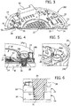
- In
Figure 1 thereference number 10 denotes overall a lighting assembly. - Various embodiments comprise, for example, a lighting assembly which uses an LED light source as a light radiation source. In various embodiments, the source may be in the form of a
set 12 of LEDs which are mounted using "Chip-on-Board" technology on asupport board 14. - In the embodiments considered here by way of a non-limiting example, the set of
LEDs 12 is shown schematically in the form of a circular shaped board mounted on a similarly circular plate orboard 14. The reference to this particular embodiment must not be interpreted as limiting in any way the scope of the description. - In various embodiments, the
board 14 may be for example of the type with a metal core. - In various embodiments, the
light radiation source electronic components 160 are mounted) able to be provided with one ormore connectors 18 so as to provide an electric power supply to theLEDs 12 and, if necessary, allow the transmission of control signals and/or transfer outside of theassembly 10 detection or sensing signals supplied by a flow sensor. - As already mentioned, in various embodiments, the
board 14 may be of the type with a metal core so that theboard 14 is able to act not only as a base body for theassembly 10, but also partly as a heat sink for dissipating externally the heat produced by the LEDs during operation. - In various embodiments, the board 14 (with the LEDs 12) and the board 16 (with the
electronic circuits 160 for driving and controlling the LEDs 12) may therefore form a compact combined structure in which the boards in question are stacked together without air gaps in between, being fixed and aligned by means of a casing to which they are joined. - In various embodiments, the
boards control circuit board 16 and the main board 14 ("populated" with arrays of LEDs which are formed for example using Chip-on-Board (CoB) technology). The resultant structure is therefore a sandwich structure consisting of several boards, which may be mechanically fixed and adjusted. - In various embodiments, the shape of the driving
board 16 may be adapted to devices mounted on themain board 14, such as an LED system of the CoB type. - In various embodiments, in order to establish the electrical connection between the
circuit board 16 and theboard 14 with theradiation source 12, one (or more)connection elements 19 may be soldered. In various embodiments these consist of flexible connection elements, of the type commonly known as Starflex, which are applied onto the CoB board, for example by means of a hot-bar or laser-soldering process. - The flexible connection between the
boards 19 may easily absorb small movements and/or vibrations of the structure, with a consequent improvement in the mechanical strength properties of the structure itself. - The
reference number 24 denotes a casing in its entirety which is for example made of molded plastic and has, in various embodiments, a bowl-like structure. - In various embodiments the
device 10 may have overall a disk-like shape. In various embodiments, such as that shown here, thecasing 24 may have a shape which may be described as being "doughnut-like". - The choice of this particular form must not, however, be interpreted as being obligatory for the purposes of implementation of the embodiments. In various embodiments, the casing 24 (and therefore the
assembly 10 as a whole) may have a different form, for example a square, rectangular or prism-like shape. - In various embodiments, in addition to an outer
peripheral wall 24b, thebottom wall 24a may be bounded internally by awall 24c defining a window 26 (which is central in the embodiments considered here by way of example) having, at least partly facing it, in the mountedassembly 10, the array ofLEDs 12, i.e. the light radiation source. The light radiation emitted by theLEDs 12 is therefore able to be emitted to the outside of theassembly 10 through thewindow 26. - In the embodiments considered here by way of example - see in particular
Figure 2 - the stack formed by theboards board 16 is mounted against theboard 14 without air gaps in between, namely in contact with theboard 14, with the set ofLEDs 12 left exposed by theboard 16, which has a ring-like shape with a central opening intended to be aligned with thewindow 26 of thecasing 24. With such an embodiment it is thus possible to obtain a stack of reduced height, having practically a height which is equal to the sum of the thicknesses of theboards - In various embodiments, the stack formed by the
board 14 and by theboard 16 is intended to be fitted in an end position onto theinternal wall formation 24c of thecasing 24. Therefore, in the mountedassembly 10, theboard 14 acts in practice as a lid or cover for thecasing 24 with theboard 16 applied against theboard 14 so as to be arranged between thebottom wall 24a and theboard 14, so that: - the
components 160 mounted on theboard 16 are housed inside the internal volume (which may be annular or doughnut-like in the embodiment considered here) of thecasing 24; and - the
LEDs 12 mounted on theboard 14 are left exposed by theboard 16 and situated opposite thewindow 26 so that the radiation produced by them is transmitted to the outside of thecasing 24. - With reference to
Figure 5 (which is essentially a view "from below" of the casing 24), the possible presence, within the saidcasing 24, of engaging formations, for example in the form ofpins bottom wall 24a of thecasing 24 and are intended to extend through corresponding openings provided in the board 16 (for example in the form ofholes 32, 33) aligned with correspondingholes Figure 3 , which shows the stack ofboards - In the embodiments considered here by way of example, the
pins 31 pass through theholes 33 and extend inside theholes 35 acting as centering elements. Thepins 31 may optionally be provided withaxial ribs 31a able to produce, together with theholes 33 and/or 35 through which they pass, an interference fit so as to help keep the twoboards - In the embodiments considered here, the
pins 30 pass through theopenings 32 until they rest in a distal position against theboard 14 and each have, passing through them, anaxial cavity 30a for receiving ascrew 36 which is able to engage inside acorresponding opening 34 in theboard 14 so as to allow fixing of thecasing 24 to theboard 14. - In various embodiments, the
screws 36 may pass completely through therespective opening 34 in theboard 14 in the axial direction (also without being screwed into it) and also extend further so as to allow fixing of theassembly 10 as a whole on a support B (Figure 4 ) such as a heat sink/support. - In various embodiments, bushes or
sleeves 38 are fitted around thescrews 36 so as to ensure that thescrews 36 act on the board 16 (and where necessary also on the board 14) only via the bushes, thereby reducing and virtually eliminating the mechanical stresses on the multiple-board structure. - In various embodiments it is also possible to choose the axial length of the
pins 30 so as to create a gap or slot between the front surface of thepins 30 and the circuit board so as to avoid any mechanical pressure on theboard 16 produced by thescrews 36 used to fix the assembly. Obviously, without affecting the principle of the invention, the embodiments and the details of construction may vary, also significantly, with respect to that illustrated here purely by way of a non-limiting example, without thereby departing from the scope of the invention as defined in the accompanying claims.
Claims (11)
- A lighting assembly (10), comprising:- a casing (24) having a bowl-like structure with a bottom wall (24a), an outer peripheral wall (24b) the bottom wall (24a) being bounded internally by a wall formation (24c) defining a window opening (26);- a radiation source board (14) with a light radiation source (12) situated opposite said opening (26) at least partly facing said opening (26) so as to direct said light radiation outside of the casing (24) to the outside of the assembly (10) through the window opening (26); and- a driving circuit board (16) for said radiation source (12);said boards (14, 16) being stacked together without air gaps in between, with said circuit board (16) directed towards said casing (24).
- The assembly as claimed in claim 1, wherein said boards (14, 16) are electrically connected together by means of flexible board connecting elements (19).
- The assembly as claimed in claim 1 or claim 2, wherein said circuit board (16) has a ring-like shape surrounding said window opening (26) with said radiation source board (14) having at least one part extending so as to close said casing (24).
- The assembly as claimed in any one of the preceding claims, wherein said opening (26) is surrounded by the wall formation (24c) of said casing (24) with said boards (14, 16) fitted onto said wall formation (24c).
- The assembly as claimed in any one of the preceding claims, wherein said casing (24) is provided with formations (30, 31) for engagement with said boards (14, 16).
- The assembly as claimed in claim 5, wherein said engaging formations comprise pins (30, 31) protruding from said casing (24), preferably from said bottom wall (24a).
- The assembly as claimed in claim 6, wherein said pins comprise pins (31) extending, preferably with an interference fit (31a), through openings (33, 35) provided in both said boards (14, 16).
- The assembly as claimed in claim 6 or claim 7, wherein said pins comprise pins (30) with cavities (30a) passed through by fixing elements (36), preferably of the screw type, which extend through openings (34) provided in said radiation source board (14).
- The assembly as claimed in claim 8, wherein bushes (38) are fitted around said fixing elements (36), so that said fixing elements (36) act on at least one of said boards (14, 16) only via said bushes (38).
- The assembly as claimed in claim 8 or claim 9, wherein a gap or slot is present between the end surface of said pins (30) with cavities (30a) and said circuit board (16).
- The assembly as claimed in any one of the preceding claims, wherein said casing (24) has a general ring-like shape.
Applications Claiming Priority (2)
| Application Number | Priority Date | Filing Date | Title |
|---|---|---|---|
| ITTO20100870 | 2010-10-29 | ||
| PCT/EP2011/068622 WO2012055852A1 (en) | 2010-10-29 | 2011-10-25 | Lighting assembly |
Publications (2)
| Publication Number | Publication Date |
|---|---|
| EP2633232A1 EP2633232A1 (en) | 2013-09-04 |
| EP2633232B1 true EP2633232B1 (en) | 2017-10-04 |
Family
ID=43738409
Family Applications (1)
| Application Number | Title | Priority Date | Filing Date |
|---|---|---|---|
| EP11782077.9A Not-in-force EP2633232B1 (en) | 2010-10-29 | 2011-10-25 | Lighting assembly |
Country Status (4)
| Country | Link |
|---|---|
| US (1) | US10094540B2 (en) |
| EP (1) | EP2633232B1 (en) |
| CN (1) | CN103189684B (en) |
| WO (1) | WO2012055852A1 (en) |
Families Citing this family (19)
| Publication number | Priority date | Publication date | Assignee | Title |
|---|---|---|---|---|
| DE102012212025A1 (en) * | 2012-07-10 | 2014-01-16 | Osram Gmbh | LIGHT MODULE |
| DE102012212027A1 (en) | 2012-07-10 | 2014-01-16 | Osram Gmbh | LIGHT MODULE |
| DE102012221229A1 (en) * | 2012-11-20 | 2014-05-22 | Osram Gmbh | Optoelectronic assembly and method for manufacturing an optoelectronic assembly |
| DE102013205998A1 (en) * | 2013-04-04 | 2014-10-09 | Osram Gmbh | Optoelectronic assembly and method for manufacturing an optoelectronic assembly |
| CN104235641B (en) * | 2013-06-09 | 2016-04-06 | 四川新力光源股份有限公司 | Ultrathin type LED light engine |
| US10072833B2 (en) * | 2013-08-13 | 2018-09-11 | Osram Opto Semiconductors Gmbh | Light apparatus with control board thermally insulated from light source |
| CN104658983B (en) * | 2013-11-22 | 2018-03-23 | 弘凯光电(深圳)有限公司 | LED load bearing seat modules |
| CN104948939A (en) * | 2014-03-27 | 2015-09-30 | 四川新力光源股份有限公司 | LED lamp and optical engine thereof |
| CN104456460A (en) * | 2014-11-20 | 2015-03-25 | 李军安 | Magnetic type LED device for warning |
| CN104565950A (en) * | 2015-01-24 | 2015-04-29 | 深圳市国源铭光电科技有限公司 | Lighting equipment |
| CN104565953A (en) * | 2015-01-24 | 2015-04-29 | 杜尉铭 | Lamp |
| EP3133332B1 (en) * | 2015-07-29 | 2018-09-12 | Tridonic Jennersdorf GmbH | Integrated led module with ims substrate |
| CN108468956A (en) * | 2017-02-23 | 2018-08-31 | 黄子恒 | The pattern of the high-quality LED light of low cost manufacturing |
| US10670250B2 (en) | 2017-12-22 | 2020-06-02 | Lumileds Llc | Chip-on-board modular lighting system and method of manufacture |
| DE102018101871A1 (en) * | 2018-01-29 | 2019-08-01 | Vossloh-Schwabe Lighting Solutions GmbH & Co. KG | Light module assembly |
| CN112204813B (en) * | 2018-05-31 | 2024-05-17 | 昕诺飞控股有限公司 | Stacked circuit board in lighting device |
| US11168870B2 (en) * | 2019-09-16 | 2021-11-09 | Xiamen Leedarson Lighting Co., Ltd | Lighting apparatus |
| US12163644B2 (en) * | 2021-10-27 | 2024-12-10 | Visual Comfort & Co. | Adjustable single-housing recessed lighting system |
| DE102024104503A1 (en) * | 2024-02-19 | 2025-08-21 | Bjb Gmbh & Co. Kg | LED connection element |
Family Cites Families (13)
| Publication number | Priority date | Publication date | Assignee | Title |
|---|---|---|---|---|
| US5909955A (en) * | 1997-03-10 | 1999-06-08 | Westek Associates | Puck style under cabinet light fixture with improved mounting ring |
| US6502968B1 (en) * | 1998-12-22 | 2003-01-07 | Mannesmann Vdo Ag | Printed circuit board having a light source |
| US7300173B2 (en) * | 2004-04-08 | 2007-11-27 | Technology Assessment Group, Inc. | Replacement illumination device for a miniature flashlight bulb |
| US7281818B2 (en) * | 2003-12-11 | 2007-10-16 | Dialight Corporation | Light reflector device for light emitting diode (LED) array |
| TWM310984U (en) * | 2006-11-28 | 2007-05-01 | Primo Lite Co Ltd | Lamp structure of light emitting diode |
| US20080212332A1 (en) * | 2007-03-01 | 2008-09-04 | Medinis David M | LED cooling system |
| DE102008016095A1 (en) * | 2008-03-28 | 2009-10-01 | Osram Opto Semiconductors Gmbh | Luminescent diode module has luminescent diode chip, which produces light during operation, light sensor which detects light incident on it during operation, and light conductor which guides light |
| CN201370898Y (en) * | 2009-01-20 | 2009-12-30 | 王少华 | LED beauty instrument |
| US8021017B2 (en) * | 2009-05-21 | 2011-09-20 | Sheng-Hsiung Cheng | LED lamp having improved heat dissipation structure |
| KR101661684B1 (en) * | 2010-04-12 | 2016-10-11 | 삼성디스플레이 주식회사 | Light source unit and back-light assembly having the same |
| KR101349841B1 (en) * | 2010-06-24 | 2014-01-09 | 엘지전자 주식회사 | LED lighting fixtures |
| US8272762B2 (en) * | 2010-09-28 | 2012-09-25 | Lighting Science Group Corporation | LED luminaire |
| US8540414B2 (en) * | 2011-09-25 | 2013-09-24 | Chin-Yi HU | Detachable LED bulb |
-
2011
- 2011-10-25 EP EP11782077.9A patent/EP2633232B1/en not_active Not-in-force
- 2011-10-25 US US13/882,469 patent/US10094540B2/en not_active Expired - Fee Related
- 2011-10-25 CN CN201180052678.9A patent/CN103189684B/en not_active Expired - Fee Related
- 2011-10-25 WO PCT/EP2011/068622 patent/WO2012055852A1/en not_active Ceased
Non-Patent Citations (1)
| Title |
|---|
| None * |
Also Published As
| Publication number | Publication date |
|---|---|
| US10094540B2 (en) | 2018-10-09 |
| US20130265779A1 (en) | 2013-10-10 |
| EP2633232A1 (en) | 2013-09-04 |
| CN103189684B (en) | 2016-08-17 |
| CN103189684A (en) | 2013-07-03 |
| WO2012055852A1 (en) | 2012-05-03 |
Similar Documents
| Publication | Publication Date | Title |
|---|---|---|
| EP2633232B1 (en) | Lighting assembly | |
| US10161577B2 (en) | Electrical connection of control circuit card to power supply in LED luminaire assembly | |
| US10816181B2 (en) | Light module providing positioning and fixation of a circuit board in a housing | |
| EP2314913A1 (en) | Light emitting unit carrier and light source comprising such a carrier | |
| EP2633226B1 (en) | Lighting assembly | |
| EP3230653B1 (en) | Led outdoor fixture in plastic housing with outer frame | |
| US20130106306A1 (en) | Lamp Unit and Luminaire | |
| JP5701429B1 (en) | lighting equipment | |
| JP6408268B2 (en) | lighting equipment | |
| US10352541B2 (en) | Integrated smart module architecture | |
| EP3133332B1 (en) | Integrated led module with ims substrate | |
| WO2018013369A1 (en) | Lighting device using wireless power transfer module | |
| JP6606716B2 (en) | lighting equipment | |
| JP2025056635A (en) | Wireless modules and electrical equipment | |
| JP6597442B2 (en) | lighting equipment | |
| US20140036513A1 (en) | Lighting device and lighting device manufacturing method | |
| WO2022153107A1 (en) | Heat radiator and electronic component module | |
| JP2023148734A (en) | lighting equipment | |
| JP2013175343A (en) | Vehicle lamp | |
| JP2016122557A (en) | LED lighting device | |
| JP2001124623A (en) | Sensor instrument | |
| JP2015220226A (en) | Lighting device |
Legal Events
| Date | Code | Title | Description |
|---|---|---|---|
| PUAI | Public reference made under article 153(3) epc to a published international application that has entered the european phase |
Free format text: ORIGINAL CODE: 0009012 |
|
| 17P | Request for examination filed |
Effective date: 20130529 |
|
| AK | Designated contracting states |
Kind code of ref document: A1 Designated state(s): AL AT BE BG CH CY CZ DE DK EE ES FI FR GB GR HR HU IE IS IT LI LT LU LV MC MK MT NL NO PL PT RO RS SE SI SK SM TR |
|
| DAX | Request for extension of the european patent (deleted) | ||
| 17Q | First examination report despatched |
Effective date: 20160909 |
|
| REG | Reference to a national code |
Ref country code: DE Ref legal event code: R079 Ref document number: 602011042137 Country of ref document: DE Free format text: PREVIOUS MAIN CLASS: F21V0019000000 Ipc: F21V0023000000 |
|
| GRAP | Despatch of communication of intention to grant a patent |
Free format text: ORIGINAL CODE: EPIDOSNIGR1 |
|
| RIC1 | Information provided on ipc code assigned before grant |
Ipc: F21V 23/00 20150101AFI20170421BHEP Ipc: F21Y 115/10 20160101ALN20170421BHEP Ipc: F21K 9/00 20160101ALI20170421BHEP Ipc: F21V 19/00 20060101ALI20170421BHEP |
|
| INTG | Intention to grant announced |
Effective date: 20170526 |
|
| GRAA | (expected) grant |
Free format text: ORIGINAL CODE: 0009210 |
|
| GRAS | Grant fee paid |
Free format text: ORIGINAL CODE: EPIDOSNIGR3 |
|
| AK | Designated contracting states |
Kind code of ref document: B1 Designated state(s): AL AT BE BG CH CY CZ DE DK EE ES FI FR GB GR HR HU IE IS IT LI LT LU LV MC MK MT NL NO PL PT RO RS SE SI SK SM TR |
|
| REG | Reference to a national code |
Ref country code: GB Ref legal event code: FG4D |
|
| REG | Reference to a national code |
Ref country code: CH Ref legal event code: EP |
|
| REG | Reference to a national code |
Ref country code: AT Ref legal event code: REF Ref document number: 934403 Country of ref document: AT Kind code of ref document: T Effective date: 20171015 |
|
| REG | Reference to a national code |
Ref country code: IE Ref legal event code: FG4D |
|
| REG | Reference to a national code |
Ref country code: DE Ref legal event code: R096 Ref document number: 602011042137 Country of ref document: DE |
|
| PGFP | Annual fee paid to national office [announced via postgrant information from national office to epo] |
Ref country code: DE Payment date: 20171019 Year of fee payment: 7 |
|
| REG | Reference to a national code |
Ref country code: NL Ref legal event code: MP Effective date: 20171004 |
|
| REG | Reference to a national code |
Ref country code: LT Ref legal event code: MG4D |
|
| REG | Reference to a national code |
Ref country code: AT Ref legal event code: MK05 Ref document number: 934403 Country of ref document: AT Kind code of ref document: T Effective date: 20171004 |
|
| PG25 | Lapsed in a contracting state [announced via postgrant information from national office to epo] |
Ref country code: NL Free format text: LAPSE BECAUSE OF FAILURE TO SUBMIT A TRANSLATION OF THE DESCRIPTION OR TO PAY THE FEE WITHIN THE PRESCRIBED TIME-LIMIT Effective date: 20171004 |
|
| PG25 | Lapsed in a contracting state [announced via postgrant information from national office to epo] |
Ref country code: LT Free format text: LAPSE BECAUSE OF FAILURE TO SUBMIT A TRANSLATION OF THE DESCRIPTION OR TO PAY THE FEE WITHIN THE PRESCRIBED TIME-LIMIT Effective date: 20171004 Ref country code: FI Free format text: LAPSE BECAUSE OF FAILURE TO SUBMIT A TRANSLATION OF THE DESCRIPTION OR TO PAY THE FEE WITHIN THE PRESCRIBED TIME-LIMIT Effective date: 20171004 Ref country code: ES Free format text: LAPSE BECAUSE OF FAILURE TO SUBMIT A TRANSLATION OF THE DESCRIPTION OR TO PAY THE FEE WITHIN THE PRESCRIBED TIME-LIMIT Effective date: 20171004 Ref country code: SE Free format text: LAPSE BECAUSE OF FAILURE TO SUBMIT A TRANSLATION OF THE DESCRIPTION OR TO PAY THE FEE WITHIN THE PRESCRIBED TIME-LIMIT Effective date: 20171004 Ref country code: NO Free format text: LAPSE BECAUSE OF FAILURE TO SUBMIT A TRANSLATION OF THE DESCRIPTION OR TO PAY THE FEE WITHIN THE PRESCRIBED TIME-LIMIT Effective date: 20180104 |
|
| PG25 | Lapsed in a contracting state [announced via postgrant information from national office to epo] |
Ref country code: IS Free format text: LAPSE BECAUSE OF FAILURE TO SUBMIT A TRANSLATION OF THE DESCRIPTION OR TO PAY THE FEE WITHIN THE PRESCRIBED TIME-LIMIT Effective date: 20180204 Ref country code: RS Free format text: LAPSE BECAUSE OF FAILURE TO SUBMIT A TRANSLATION OF THE DESCRIPTION OR TO PAY THE FEE WITHIN THE PRESCRIBED TIME-LIMIT Effective date: 20171004 Ref country code: LV Free format text: LAPSE BECAUSE OF FAILURE TO SUBMIT A TRANSLATION OF THE DESCRIPTION OR TO PAY THE FEE WITHIN THE PRESCRIBED TIME-LIMIT Effective date: 20171004 Ref country code: HR Free format text: LAPSE BECAUSE OF FAILURE TO SUBMIT A TRANSLATION OF THE DESCRIPTION OR TO PAY THE FEE WITHIN THE PRESCRIBED TIME-LIMIT Effective date: 20171004 Ref country code: GR Free format text: LAPSE BECAUSE OF FAILURE TO SUBMIT A TRANSLATION OF THE DESCRIPTION OR TO PAY THE FEE WITHIN THE PRESCRIBED TIME-LIMIT Effective date: 20180105 Ref country code: BG Free format text: LAPSE BECAUSE OF FAILURE TO SUBMIT A TRANSLATION OF THE DESCRIPTION OR TO PAY THE FEE WITHIN THE PRESCRIBED TIME-LIMIT Effective date: 20180104 Ref country code: AT Free format text: LAPSE BECAUSE OF FAILURE TO SUBMIT A TRANSLATION OF THE DESCRIPTION OR TO PAY THE FEE WITHIN THE PRESCRIBED TIME-LIMIT Effective date: 20171004 |
|
| REG | Reference to a national code |
Ref country code: CH Ref legal event code: PL |
|
| REG | Reference to a national code |
Ref country code: DE Ref legal event code: R097 Ref document number: 602011042137 Country of ref document: DE |
|
| REG | Reference to a national code |
Ref country code: IE Ref legal event code: MM4A |
|
| PG25 | Lapsed in a contracting state [announced via postgrant information from national office to epo] |
Ref country code: CH Free format text: LAPSE BECAUSE OF NON-PAYMENT OF DUE FEES Effective date: 20171031 Ref country code: EE Free format text: LAPSE BECAUSE OF FAILURE TO SUBMIT A TRANSLATION OF THE DESCRIPTION OR TO PAY THE FEE WITHIN THE PRESCRIBED TIME-LIMIT Effective date: 20171004 Ref country code: SK Free format text: LAPSE BECAUSE OF FAILURE TO SUBMIT A TRANSLATION OF THE DESCRIPTION OR TO PAY THE FEE WITHIN THE PRESCRIBED TIME-LIMIT Effective date: 20171004 Ref country code: DK Free format text: LAPSE BECAUSE OF FAILURE TO SUBMIT A TRANSLATION OF THE DESCRIPTION OR TO PAY THE FEE WITHIN THE PRESCRIBED TIME-LIMIT Effective date: 20171004 Ref country code: LU Free format text: LAPSE BECAUSE OF NON-PAYMENT OF DUE FEES Effective date: 20171025 Ref country code: MC Free format text: LAPSE BECAUSE OF FAILURE TO SUBMIT A TRANSLATION OF THE DESCRIPTION OR TO PAY THE FEE WITHIN THE PRESCRIBED TIME-LIMIT Effective date: 20171004 Ref country code: LI Free format text: LAPSE BECAUSE OF NON-PAYMENT OF DUE FEES Effective date: 20171031 Ref country code: CZ Free format text: LAPSE BECAUSE OF FAILURE TO SUBMIT A TRANSLATION OF THE DESCRIPTION OR TO PAY THE FEE WITHIN THE PRESCRIBED TIME-LIMIT Effective date: 20171004 |
|
| PLBE | No opposition filed within time limit |
Free format text: ORIGINAL CODE: 0009261 |
|
| STAA | Information on the status of an ep patent application or granted ep patent |
Free format text: STATUS: NO OPPOSITION FILED WITHIN TIME LIMIT |
|
| REG | Reference to a national code |
Ref country code: BE Ref legal event code: MM Effective date: 20171031 |
|
| PG25 | Lapsed in a contracting state [announced via postgrant information from national office to epo] |
Ref country code: PL Free format text: LAPSE BECAUSE OF FAILURE TO SUBMIT A TRANSLATION OF THE DESCRIPTION OR TO PAY THE FEE WITHIN THE PRESCRIBED TIME-LIMIT Effective date: 20171004 Ref country code: SM Free format text: LAPSE BECAUSE OF FAILURE TO SUBMIT A TRANSLATION OF THE DESCRIPTION OR TO PAY THE FEE WITHIN THE PRESCRIBED TIME-LIMIT Effective date: 20171004 Ref country code: IT Free format text: LAPSE BECAUSE OF FAILURE TO SUBMIT A TRANSLATION OF THE DESCRIPTION OR TO PAY THE FEE WITHIN THE PRESCRIBED TIME-LIMIT Effective date: 20171004 Ref country code: BE Free format text: LAPSE BECAUSE OF NON-PAYMENT OF DUE FEES Effective date: 20171031 Ref country code: RO Free format text: LAPSE BECAUSE OF FAILURE TO SUBMIT A TRANSLATION OF THE DESCRIPTION OR TO PAY THE FEE WITHIN THE PRESCRIBED TIME-LIMIT Effective date: 20171004 |
|
| REG | Reference to a national code |
Ref country code: FR Ref legal event code: ST Effective date: 20180727 |
|
| 26N | No opposition filed |
Effective date: 20180705 |
|
| GBPC | Gb: european patent ceased through non-payment of renewal fee |
Effective date: 20180104 |
|
| PG25 | Lapsed in a contracting state [announced via postgrant information from national office to epo] |
Ref country code: MT Free format text: LAPSE BECAUSE OF NON-PAYMENT OF DUE FEES Effective date: 20171025 |
|
| PG25 | Lapsed in a contracting state [announced via postgrant information from national office to epo] |
Ref country code: IE Free format text: LAPSE BECAUSE OF NON-PAYMENT OF DUE FEES Effective date: 20171025 Ref country code: FR Free format text: LAPSE BECAUSE OF NON-PAYMENT OF DUE FEES Effective date: 20171204 |
|
| PG25 | Lapsed in a contracting state [announced via postgrant information from national office to epo] |
Ref country code: SI Free format text: LAPSE BECAUSE OF FAILURE TO SUBMIT A TRANSLATION OF THE DESCRIPTION OR TO PAY THE FEE WITHIN THE PRESCRIBED TIME-LIMIT Effective date: 20171004 Ref country code: GB Free format text: LAPSE BECAUSE OF NON-PAYMENT OF DUE FEES Effective date: 20180104 |
|
| REG | Reference to a national code |
Ref country code: DE Ref legal event code: R119 Ref document number: 602011042137 Country of ref document: DE |
|
| PG25 | Lapsed in a contracting state [announced via postgrant information from national office to epo] |
Ref country code: HU Free format text: LAPSE BECAUSE OF FAILURE TO SUBMIT A TRANSLATION OF THE DESCRIPTION OR TO PAY THE FEE WITHIN THE PRESCRIBED TIME-LIMIT; INVALID AB INITIO Effective date: 20111025 |
|
| PG25 | Lapsed in a contracting state [announced via postgrant information from national office to epo] |
Ref country code: DE Free format text: LAPSE BECAUSE OF NON-PAYMENT OF DUE FEES Effective date: 20190501 |
|
| PG25 | Lapsed in a contracting state [announced via postgrant information from national office to epo] |
Ref country code: CY Free format text: LAPSE BECAUSE OF NON-PAYMENT OF DUE FEES Effective date: 20171004 |
|
| PG25 | Lapsed in a contracting state [announced via postgrant information from national office to epo] |
Ref country code: MK Free format text: LAPSE BECAUSE OF FAILURE TO SUBMIT A TRANSLATION OF THE DESCRIPTION OR TO PAY THE FEE WITHIN THE PRESCRIBED TIME-LIMIT Effective date: 20171004 |
|
| PG25 | Lapsed in a contracting state [announced via postgrant information from national office to epo] |
Ref country code: TR Free format text: LAPSE BECAUSE OF FAILURE TO SUBMIT A TRANSLATION OF THE DESCRIPTION OR TO PAY THE FEE WITHIN THE PRESCRIBED TIME-LIMIT Effective date: 20171004 |
|
| PG25 | Lapsed in a contracting state [announced via postgrant information from national office to epo] |
Ref country code: PT Free format text: LAPSE BECAUSE OF FAILURE TO SUBMIT A TRANSLATION OF THE DESCRIPTION OR TO PAY THE FEE WITHIN THE PRESCRIBED TIME-LIMIT Effective date: 20171004 |
|
| PG25 | Lapsed in a contracting state [announced via postgrant information from national office to epo] |
Ref country code: AL Free format text: LAPSE BECAUSE OF FAILURE TO SUBMIT A TRANSLATION OF THE DESCRIPTION OR TO PAY THE FEE WITHIN THE PRESCRIBED TIME-LIMIT Effective date: 20171004 |