EP2629327A2 - Semiconductor manufacturing apparatus - Google Patents
Semiconductor manufacturing apparatus Download PDFInfo
- Publication number
- EP2629327A2 EP2629327A2 EP13155303.4A EP13155303A EP2629327A2 EP 2629327 A2 EP2629327 A2 EP 2629327A2 EP 13155303 A EP13155303 A EP 13155303A EP 2629327 A2 EP2629327 A2 EP 2629327A2
- Authority
- EP
- European Patent Office
- Prior art keywords
- carrier body
- manufacturing apparatus
- semiconductor manufacturing
- inner bottom
- Prior art date
- Legal status (The legal status is an assumption and is not a legal conclusion. Google has not performed a legal analysis and makes no representation as to the accuracy of the status listed.)
- Granted
Links
Images



Classifications
-
- H—ELECTRICITY
- H10—SEMICONDUCTOR DEVICES; ELECTRIC SOLID-STATE DEVICES NOT OTHERWISE PROVIDED FOR
- H10P—GENERIC PROCESSES OR APPARATUS FOR THE MANUFACTURE OR TREATMENT OF DEVICES COVERED BY CLASS H10
- H10P72/00—Handling or holding of wafers, substrates or devices during manufacture or treatment thereof
- H10P72/70—Handling or holding of wafers, substrates or devices during manufacture or treatment thereof for supporting or gripping
- H10P72/76—Handling or holding of wafers, substrates or devices during manufacture or treatment thereof for supporting or gripping using mechanical means, e.g. clamps or pinches
- H10P72/7604—Handling or holding of wafers, substrates or devices during manufacture or treatment thereof for supporting or gripping using mechanical means, e.g. clamps or pinches the wafers being placed on a susceptor, stage or support
- H10P72/7624—Handling or holding of wafers, substrates or devices during manufacture or treatment thereof for supporting or gripping using mechanical means, e.g. clamps or pinches the wafers being placed on a susceptor, stage or support characterised by the mechanical construction of the susceptor, stage or support
-
- B—PERFORMING OPERATIONS; TRANSPORTING
- B05—SPRAYING OR ATOMISING IN GENERAL; APPLYING FLUENT MATERIALS TO SURFACES, IN GENERAL
- B05C—APPARATUS FOR APPLYING FLUENT MATERIALS TO SURFACES, IN GENERAL
- B05C13/00—Means for manipulating or holding work, e.g. for separate articles
- B05C13/02—Means for manipulating or holding work, e.g. for separate articles for particular articles
-
- H—ELECTRICITY
- H10—SEMICONDUCTOR DEVICES; ELECTRIC SOLID-STATE DEVICES NOT OTHERWISE PROVIDED FOR
- H10P—GENERIC PROCESSES OR APPARATUS FOR THE MANUFACTURE OR TREATMENT OF DEVICES COVERED BY CLASS H10
- H10P72/00—Handling or holding of wafers, substrates or devices during manufacture or treatment thereof
- H10P72/70—Handling or holding of wafers, substrates or devices during manufacture or treatment thereof for supporting or gripping
- H10P72/76—Handling or holding of wafers, substrates or devices during manufacture or treatment thereof for supporting or gripping using mechanical means, e.g. clamps or pinches
- H10P72/7604—Handling or holding of wafers, substrates or devices during manufacture or treatment thereof for supporting or gripping using mechanical means, e.g. clamps or pinches the wafers being placed on a susceptor, stage or support
- H10P72/7611—Handling or holding of wafers, substrates or devices during manufacture or treatment thereof for supporting or gripping using mechanical means, e.g. clamps or pinches the wafers being placed on a susceptor, stage or support characterised by edge profile or support profile
-
- H—ELECTRICITY
- H10—SEMICONDUCTOR DEVICES; ELECTRIC SOLID-STATE DEVICES NOT OTHERWISE PROVIDED FOR
- H10P—GENERIC PROCESSES OR APPARATUS FOR THE MANUFACTURE OR TREATMENT OF DEVICES COVERED BY CLASS H10
- H10P72/00—Handling or holding of wafers, substrates or devices during manufacture or treatment thereof
- H10P72/70—Handling or holding of wafers, substrates or devices during manufacture or treatment thereof for supporting or gripping
- H10P72/76—Handling or holding of wafers, substrates or devices during manufacture or treatment thereof for supporting or gripping using mechanical means, e.g. clamps or pinches
- H10P72/7604—Handling or holding of wafers, substrates or devices during manufacture or treatment thereof for supporting or gripping using mechanical means, e.g. clamps or pinches the wafers being placed on a susceptor, stage or support
- H10P72/7618—Handling or holding of wafers, substrates or devices during manufacture or treatment thereof for supporting or gripping using mechanical means, e.g. clamps or pinches the wafers being placed on a susceptor, stage or support characterised by a movable susceptor, stage or support, others than those only rotating on their own vertical axis, e.g. susceptors on a rotating carrousel
-
- H—ELECTRICITY
- H10—SEMICONDUCTOR DEVICES; ELECTRIC SOLID-STATE DEVICES NOT OTHERWISE PROVIDED FOR
- H10P—GENERIC PROCESSES OR APPARATUS FOR THE MANUFACTURE OR TREATMENT OF DEVICES COVERED BY CLASS H10
- H10P72/00—Handling or holding of wafers, substrates or devices during manufacture or treatment thereof
- H10P72/70—Handling or holding of wafers, substrates or devices during manufacture or treatment thereof for supporting or gripping
- H10P72/76—Handling or holding of wafers, substrates or devices during manufacture or treatment thereof for supporting or gripping using mechanical means, e.g. clamps or pinches
- H10P72/7604—Handling or holding of wafers, substrates or devices during manufacture or treatment thereof for supporting or gripping using mechanical means, e.g. clamps or pinches the wafers being placed on a susceptor, stage or support
- H10P72/7621—Handling or holding of wafers, substrates or devices during manufacture or treatment thereof for supporting or gripping using mechanical means, e.g. clamps or pinches the wafers being placed on a susceptor, stage or support characterised by supporting two or more semiconductor substrates
Definitions
- a present invention relates to a semiconductor manufacturing apparatus.
- FIG. 1 is a cross-sectional view of a general semiconductor manufacturing apparatus.
- a semiconductor manufacturing apparatus 100 includes a source 110, a reaction chamber 120, a wafer carrier (or a susceptor) 130, a rotary shaft 150, a heating unit 160 such as a heater, and a shroud 170.
- the wafer carrier 130 is disposed within the reaction chamber 120, and includes at least one pocket 140 formed on the upper portion thereof.
- a wafer (not shown) is loaded in the pocket 140, and the rotary shaft 150 is coupled with the lower portion of the wafer carrier 130 and rotates the wafer carrier 130.
- the heating unit 160 heats the lower portion of the wafer carrier 130 and the inside of the reaction chamber 120 to a designated temperature.
- the shroud 170 serves to supply a source material from the source 110 to the reaction chamber 120.
- a semiconductor thin film or an insulating film, etc may be grown on the surface of the wafer (not shown) by chemical reaction of the source material introduced into the reaction chamber 120.
- the semiconductor manufacturing apparatus 100 may grow devices, such as gallium nitride-based semiconductor light emitting devices, high electron mobility transistors (HEMTs), field effect transistors (FETs) or laser diodes, on the surface of the wafer using metal organic chemical vapor deposition (MOCVD), molecular beam epitaxy (MBE), or chemical vapor deposition (CVD).
- devices such as gallium nitride-based semiconductor light emitting devices, high electron mobility transistors (HEMTs), field effect transistors (FETs) or laser diodes, on the surface of the wafer using metal organic chemical vapor deposition (MOCVD), molecular beam epitaxy (MBE), or chemical vapor deposition (CVD).
- MOCVD metal organic chemical vapor deposition
- MBE molecular beam epitaxy
- CVD chemical vapor deposition
- the wafer carrier 130 may be formed of carbon or aluminium nitride (AIN), and the surface of the wafer carrier 130 and the surface of the wafer carrier 130 contacting the wafer within the pocket 140 may be coated with a silicon carbide (SiC) film, a carbon film, or an AIN film.
- SiC silicon carbide
- AIN aluminium nitride
- the pockets 140 are formed integrally with the body of the wafer carrier 130 of the semiconductor manufacturing apparatus 100, and are not separated from the wafer carrier 130. Thereby, even if only one of the plural pockets 140 is damaged, the entirety of the wafer carrier 130 needs to be replaced.
- the plural pockets 140 located on the wafer carrier 130 are heated to different temperatures according to positions of the pockets 140. Nonetheless, since the plural pockets 140 have the same shape, uniform growth of a material on wafers may be difficult according to the positions of the pockets 140.
- the present invention provides a semiconductor manufacturing apparatus which may detachably attach pockets to a wafer carrier and have various shapes of the pockets.
- a semiconductor manufacturing apparatus includes at least one pocket on which a passive subject on which deposition will be executed is mounted, and a carrier body having an insertion space to which the at least one pocket is detachably attached.
- the at least one pocket may include plural pockets, and depths of insertion of the plural pockets into the carrier body may be different or equal according to the plural pockets.
- the insertion space may be formed in the shape of a hole passing through the carrier body, or in the shape of a groove formed on the upper surface of the carrier body.
- the at least one pocket may include a front support part formed on a front surface of the at least one pocket and supporting the passive subject and a rear coupling part formed on a rear surface of the at least one pocket and coupled with the carrier body, and the carrier body and the rear coupling part may have shapes corresponding to each other so as to be coupled with each other.
- the front support part may include a first inner side surface extended in a first direction in which the at least one pocket is inserted into the carrier body, a first inner bottom surface extended from the first inner side surface in a second direction different from the first direction, the edge of the passive subject being placed on the first inner bottom surface, and a second inner side surface extended from the first inner bottom surface in the first direction.
- the front support part may further include a second inner bottom surface extended from the second inner side surface in the second direction and corresponding to a bottom of the at least one pocket.
- At least one of the first and second inner bottom surfaces may have a convex or concave shape toward the passive subject, or have at least one stepped portion.
- the rear coupling part may include a first outer side surface extended in the first direction on the side of the at least one pocket opposite to the first inner side surface, a first outer bottom surface extended from the first outer side surface in the second direction on the side of the at least one pocket opposite to the first inner bottom surface, and a second outer side surface extended from the first outer bottom surface in the first direction on the side of the at least one pocket opposite to the second inner side surface.
- the rear coupling part may further include a second outer bottom surface extended from the second outer side surface in the second direction on the side of the at least one pocket opposite to the second inner bottom surface.
- the carrier body may include a third inner side surface facing the first outer side surface and extended in the first direction, a third inner bottom surface facing the first outer bottom surface and extended from the third inner side surface in the second direction, and a fourth inner side surface facing the second outer side surface and extended from the third inner bottom surface in the first direction.
- the carrier body may further include a fourth inner bottom surface facing the second outer bottom surface and extended from the fourth inner side surface in the second direction.
- the fourth inner bottom surface may have a convex or concave shape toward the passive subject, or have at least one stepped portion.
- the carrier body may further include a third outer bottom surface opposite to the fourth inner bottom surface, the third outer bottom surface having at least one stepped portion.
- the at least one pocket may include a support projection protruded from the first outer bottom surface toward the third inner bottom surface of the carrier body, and the carrier body may include a support groove formed on the third inner bottom surface so that the support projection of the at least one pocket may be inserted into the support groove.
- the rear coupling part may have an outer side wall provided with a male screw thread formed thereon
- the carrier body may have an inner side wall provided with a female screw thread formed thereon
- the rear coupling part and the carrier body may be coupled by engaging the male screw thread and the female screw thread.
- At least one scale mark may be formed on the upper edge surface of the at least one pocket, and at least one indicator may be formed on the upper edge of the carrier body neighboring the upper edge surface.
- the rear coupling part may include a coupling projection protruded in the second direction different from the first direction in which the at least one pocket is inserted into the carrier body, and the carrier body may include at least one coupling groove being proper to fix the coupling projection when the at least one pocket is pressed in the first direction.
- the at least one coupling groove may include plural coupling grooves separated from each other by a designated interval.
- scale marks indicating a depth of insertion of the at least one pocket into the carrier body may be formed on an outer side wall of the rear coupling part.
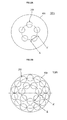
- FIGs. 2A and 2B are plan views of wafer carriers (or susceptors) 200A and 200B in accordance with the present invention.
- Pockets 300 arranged in one concentric circular line around the center of the wafer carrier 200A, as shown in FIG. 2A , or pockets 300 arranged in two concentric circular lines around the center of the wafer carrier 200B, as shown in FIG. 2B , may be formed on the surface of a carrier body 400 of the wafer carrier 200A or 200B.
- the arrangement shape of the pockets 300, the shape of each pocket 300 and the number of the pockets 300 on the wafer carriers 200A and 200B are not limited thereto.
- the pockets 300 may be arranged on the carrier body 400 in a shape other than one concentric circular line or two concentric circular lines. Further, 1 to 50 or more pockets 300 may be arranged on the wafer carrier 200A or 200B according to the size of a passive subject, i.e., wafer, on which deposition will be executed, mounted on each pocket 300 or the capacity of a reaction chamber. Still further, the pocket 300 may be formed in a circular shape or in a flat structure obtained by cutting one end of a circular shape.
- a shaft-coupling groove (not shown) is formed at the center of the lower surface of the wafer carrier 200A or 200B, and for example, the rotary shaft 150, as shown in FIG. 1 , may be coupled with the shaft-coupling groove.
- the wafer carrier 200A or 200B exemplarily shown in FIG. 2A or 2B may be disposed within the chamber 120 in the same manner as the wafer carrier 130 shown in FIG. 1 , this present invention is not limited thereto.
- the carrier body 400 has insertion spaces corresponding in number to the number of the pockets 300, and each insertion space has a structure to which the pocket 300 may be detachably attached.
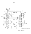
- FIG. 3 is a partial exploded view of a cross-section taken along the line A-A' of a pocket 300 and a carrier body 400 exemplarily shown in FIG. 2A or 2B in accordance with the present invention.
- the pocket 300 in accordance with this present invention includes a front support part 310 and a rear coupling part 320.
- the front support part 310 serves to support a wafer 500, and includes a first inner side surface 312, a first inner bottom surface 314, a second inner side surface 316 and a second inner bottom surface 318.
- the first inner side surface 312 is extended in a first direction in which the pocket 300 is inserted into the carrier body 400.
- the first inner bottom surface 314 is extended from the first inner side surface 312 in a second direction different from the first direction, and an edge 502 of the wafer 500 is placed on the first inner bottom surface 314.
- the edge 502 of the wafer 500 may be placed on the first inner bottom surface 314, and a separation distance d1 between a front end 504 of the wafer 500 and the first inner side surface 312 may be '0' or more.
- the first direction and the second direction may be perpendicular to each other.
- the second inner side surface 316 is extended from the first inner bottom surface 314 in a third direction.
- the third direction may be identical with the first direction, the disclosure is not limited thereto.
- the second inner bottom surface 318 is extended from the second inner side surface 316 in a fourth direction, and corresponds to the bottom of the pocket 300.
- fourth direction may be identical with the second direction, the disclosure is not limited thereto.
- the wafer carrier may further include a first fixing part (not shown) fixing the wafer 500 and the pocket 300, a second fixing part (not shown) fixing the pocket 300 and the carrier body 400, or a third fixing part (not shown) simultaneously fixing the wafer 500, the pocket 300 and the carrier body 400.
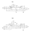
- FIGs. 4 to 9 and FIG. 11 are partial cross-sectional views taken along the line A-A' of pockets 300 and carrier bodies 400 exemplarily shown in FIG. 2A or 2B in accordance with the present invention.
- the second inner bottom surface 318 exemplarily shown in FIG. 3 may be omitted.
- the pocket 300 may be formed in a hole shape having no bottom, as exemplarily shown in FIG. 4 or 8 .
- first and second inner bottom surfaces 314 and 318 may have a convex shape or a concave shape toward the wafer 500.
- the second inner bottom surface 318 may have a convex shape toward the wafer 500, as exemplarily shown in FIG. 5 , or have a concave shape toward the wafer 500, as exemplarily shown in FIG. 6 .
- At least one of the first and second inner bottom surfaces 314 and 318 may have at least one stepped portion.
- a groove 340 is formed at the edge of the second inner bottom surface 318, as exemplarily shown in FIG. 7
- a bottom surface 342 of the edge of the second inner bottom surface 318 has a stepped difference with the center of the second inner bottom surface 318.
- at least one of the first and second inner bottom surfaces 314 and 318 may have an inclined shape.
- the reason why the shape of at least one of the first and second inner bottom surfaces 314 and 318 is varied is to uniformize different temperatures of the edge and the center of the wafer 500, during the growth of the wafer 500, for example, when the wafer 500 is heated by the heating unit 160 exemplarily shown in FIG. 1 .
- the rear coupling part 320 of the pocket 300 is coupled with the carrier body 400 on the rear surface of the pocket 300.
- the rear coupling part 320 and the carrier body 400 have shapes corresponding to each other so as to be coupled with each other.
- the rear coupling part 320 includes a first outer side surface 322, a first outer bottom surface 324, a second outer side surface 326 and a second outer bottom surface 328.
- the first outer side surface 322 is extended in a fifth direction on the side of the pocket 300 opposite to the first inner side surface 312.
- the fifth direction may be identical with the first direction, the disclosure is not limited thereto.
- the first outer bottom surface 324 is extended from the first outer side surface 322 in a sixth direction different from the fifth direction on the side of the pocket 300 opposite to the first inner bottom surface 314.
- the sixth direction may be identical with the second direction, the disclosure is not limited thereto.
- the second outer side surface 326 is extended from the first outer bottom surface 324 in a seventh direction on the side of the pocket 300 opposite to the second inner side surface 316.
- the seventh direction may be identical with the first direction, the disclosure is not limited thereto.
- the second outer bottom surface 328 is extended from the second outer side surface 326 in an eighth direction on the side of the pocket 300 opposite to the second inner bottom surface 318.
- eighth direction may be identical with the second direction, the disclosure is not limited thereto.
- the second outer bottom surface 328 may also be omitted from the rear coupling part 320, as exemplarily shown in FIG. 4 or 8 .
- the carrier body 400 may include a third inner side surface 412, a third inner bottom surface 414, a fourth inner side surface 416, a fourth inner bottom surface 420 and a third outer bottom surface 440.
- the third inner side surface 412 faces the first outer side surface 322, and is extended in a ninth direction.
- the ninth direction may be the first direction, the disclosure is not limited thereto.
- the third inner bottom surface 414 faces the first outer bottom surface 324, and is extended from the third inner side surface 412 in a tenth direction.
- the tenth direction may be the second direction, the disclosure is not limited thereto.
- the fourth inner side surface 416 faces the second outer side surface 326, and is extended from the third inner bottom surface 414 in an eleventh direction.
- the eleventh direction may be the first direction, the disclosure is not limited thereto.
- a separation distance d2 between the third inner side surface 412 and the first outer side surface 322 may be '0' or more
- a separation distance d3 between the fourth inner side surface 416 and the second outer side surface 326 may be '0' or more.
- the fourth inner bottom surface 420 faces the second outer bottom surface 328, and is extended from the fourth inner side surface 416 in a twelfth direction.
- twelfth direction may be the second direction, the disclosure is not limited thereto.
- At least one of the third and fourth inner bottom surfaces 414 and 420 may have a flat shape, as exemplarily shown in FIG. 3 , have a convex shape or a concave shape, or have at least one stepped portion.
- the fourth inner bottom surface 420 may have a convex shape toward the wafer 500, as exemplarily shown in FIG. 4 .
- the fourth inner bottom surface 420 may have a concave shape toward the wafer 500.
- the third outer bottom surface 440 may be located at the side of the wafer body 400 opposite to the fourth inner bottom surface 420, and have at least one stepped portion.
- the third outer bottom surface 440 may have a stepped portion, as exemplarily shown in FIG. 6 .
- the space 402 into which the above-described pocket 300 is inserted may be formed in the shape of a groove formed on the upper surface of the carrier body 400.
- the carrier body 400 has the fourth inner bottom surface 420 and the third outer bottom surface 440, as exemplarily shown in FIG. 3 , 4 or 6 .
- the insertion space 402 may be formed in the shape of a hole passing through the carrier body 400.
- the fourth inner bottom surface 420 and the third outer bottom surface 440 are omitted from the carrier body 400, as exemplarily shown in FIG. 5 , 7 , 8 , 9 or 11 .
- the reason why the shape of at least one of the third inner bottom surface 414, the fourth inner bottom surface 420 and the third outer bottom surface 440 of the carrier body 400 is varied is to uniformize different temperatures of the edge and the center of the wafer 500, during the growth of the wafer 500, for example, when the wafer 500 is heated by the heating unit 160 exemplarily shown in FIG. 1 .
- a first height h1 of the second outer side surface 326 may be '0' or more. If the first height h1 is '0' or more, the wafer 500 is placed on the first and second inner bottom surfaces 314 and 318.
- first height h1 of the second outer side surface 326 may be equal to or smaller than a second height h2 of the fourth inner side surface 416.
- first height h1 becomes gradually smaller than the second height h2
- the temperature around the center of the pocket 300 rather than the edge of the pocket 300 is relatively lowered.
- the area of a region where the center of the pocket 300 and the carrier body 400 are opposite to each other is smaller than the area of a region where the edge of the pocket 300 and the carrier body 400 are opposite to each other and thus a smaller amount of heat from the carrier body 400 is transmitted to the center of the pocket 300 than the edge of the pocket 300.
- a third height h3 of the first outer side surface 322 and a fourth height h4 of the third inner side surface 412 may be equal or different.
- the insertion depths of the plural pockets 300 into the carrier body 400 may be equal or different. Namely, at least one of a difference ⁇ h1 between the first height h1 and the second height h2 and a difference ⁇ h2 between the third height h3 and the fourth height h4 may be uniform or varied according to the plural pockets 300.
- the reason why the first to fourth heights h1 to h4 are varied is to uniformize different temperatures of the edge and the center of the wafer 500, during the growth of the wafer 500, for example, when the wafer 500 is heated by the heating unit 160 exemplarily shown in FIG. 1 .
- a temperature difference between the edge and the center of the wafer 500 may be compensated for by adjusting a thickness t1 of the bottom of the pocket 300 and a thickness t2 of the bottom of the carrier body 400 exemplarily shown in FIG. 3 .
- the thickness t1 of the bottom of the pocket 300 is varied according to the edge and the center of the pocket 300, as exemplarily shown in FIG. 5 , 6 or 7 , the temperature of the edge of the wafer 500 and the temperature of the center of the wafer 500 may become uniform.
- the thickness t2 of the bottom of the carrier body 400 is varied according to the edge and the center of the carrier body 400, as exemplarily shown in FIG. 4 or 6 , the temperature of the edge of the wafer 500 and the temperature of the center of the wafer 500 may become uniform.
- the pocket 300 may be separated from the carrier body 400 by centrifugal force when the wafer carrier 200A or 200B is rotated after the above-described pocket 300 is coupled with the carrier body 400.
- the pocket 300 may further include a support projection
- the carrier body 400 may further include a support groove.
- a support projection 330 of the pocket 300 may be protruded from the first outer bottom surface 324 toward the third inner bottom surface 414 of the carrier body 400.
- a support groove 430 may be formed on the third inner bottom surface 414 so that the support projection 330 of the pocket 300 may be inserted into the support groove 430.
- a support projection (not shown) of the pocket 300 may be protruded from the first outer side surface 322 toward the third inner side surface 412 of the carrier body 400.
- a support groove (not shown) may be formed on the third inner side surface 412 so that the support projection (not shown) of the pocket 300 may be inserted into the support groove (not shown).
- the rear coupling part 320 and an inner side wall 410 of the carrier body 400 may be coupled with each other by bent shapes thereof.
- the disclosure is not limited thereto, and the pocket 300 may be detachably attached to the carrier body 400 in various shapes.
- the outer side wall of the circular pocket 300 may have a male screw thread shape
- the inner side wall of the carrier body 400 may have a female screw thread shape
- the rear coupling part 350 of the pocket 300 has an outer side wall 352 provided with a male screw thread formed thereon
- the carrier body 400 has an inner side wall 450 provided with a female screw thread formed thereon. Therefore, the outer side wall 352 of the rear coupling part 350 and the inner side wall 450 of the carrier body 400 may be coupled by connection between the male screw thread and the female screw thread.
- outer side wall 352 of the rear coupling part 350 and the inner side wall 450 of the carrier body 400 are not limited to the above-described screw thread shapes.
- the outer side wall 352 and the inner side wall 450 may have various shapes, such as a right-handed screw thread and a left-handed screw thread.
- FIG. 10 is a schematic plan view of the pocket 300 exemplarily shown in FIG. 9 .
- At least one scale mark 302 may be formed on an upper edge surface 311 of the pocket 300, and at least one indicator 402 may be formed on the upper edge of the carrier body 400 neighboring the upper edge surface 311 of the pocket 300. Therefore, when the male screw thread-shaped pocket 300 is rotated in the clockwise or counterclockwise direction and is inserted into the female screw thread-shaped carrier body 400, the rotating degree of the pocket 300, i.e., the insertion depth of the pocket 300 into the carrier body 400, may be estimated by observing the scale marks 302 based on the indicators 402. For this purpose, the number '0' may be expressed at one of the scale marks 302.
- the rear coupling part of the pocket 300 may have a coupling projection 360, and the carrier body 400 may have at least one coupling groove 460. Therefore, when at least one pocket 300 is pressed in the first direction, the at least one pocket 300 may be coupled with the carrier body 400 by fixing the coupling projection 360 to the at least one coupling groove 460.
- the coupling projection 360 of the pocket 300 is protruded in the second direction different from the first direction in which the pocket 300 is inserted into the carrier body 400.
- the at least one coupling groove 460 has a proper shape to fix the coupling projection 360 thereto, and is formed on the inner side wall of the carrier body 400.
- the at least one coupling groove 460 may be plural coupling grooves separated from each other by a designated interval.
- first to third coupling grooves 462, 464 and 466 are formed at a designated interval.
- scale marks 370 for measurement of a depth of the insertion of the pocket 300 into the carrier body 400 may be formed on the outer side wall of the rear coupling part of the pocket 300. Namely, which coupling groove among the first to third coupling grooves 462, 464 and 466 into which the coupling protrusion 360 is inserted may be estimated through the number of the exposed scale marks 370 when the coupling protrusion 360 is inserted into the first coupling groove 462 located at the uppermost end of the inner side wall of the carrier body 400, the number of the exposed scale marks 370 when the coupling protrusion 360 is inserted into the second coupling groove 464 located under the first coupling groove 462, and the number of the exposed scale marks 370 when the coupling protrusion 360 is inserted into the third coupling groove 466 located under the second coupling groove 464.
- a semiconductor manufacturing apparatus in accordance with the present invention may attach and detach pockets to and from a wafer carrier and, if a pocket is damaged, the damaged pocket alone may be replaced without replacement of the entirety of the wafer carrier including the damaged pocket, thereby shortening process time and reducing process expenses. Further, the semiconductor manufacturing apparatus allows the pockets to have different structures according to the positions of the pockets on the wafer carrier so that the uniform growth of a material may be achieved on the surfaces of wafers regardless of the positions of the pockets.
Landscapes
- Container, Conveyance, Adherence, Positioning, Of Wafer (AREA)
- Packaging Frangible Articles (AREA)
- Chemical Vapour Deposition (AREA)
Abstract
Description
- A present invention relates to a semiconductor manufacturing apparatus.
-
FIG. 1 is a cross-sectional view of a general semiconductor manufacturing apparatus. - With reference to
FIG. 1 , asemiconductor manufacturing apparatus 100 includes asource 110, areaction chamber 120, a wafer carrier (or a susceptor) 130, arotary shaft 150, aheating unit 160 such as a heater, and ashroud 170. - The
wafer carrier 130 is disposed within thereaction chamber 120, and includes at least onepocket 140 formed on the upper portion thereof. A wafer (not shown) is loaded in thepocket 140, and therotary shaft 150 is coupled with the lower portion of thewafer carrier 130 and rotates thewafer carrier 130. - The
heating unit 160 heats the lower portion of thewafer carrier 130 and the inside of thereaction chamber 120 to a designated temperature. Theshroud 170 serves to supply a source material from thesource 110 to thereaction chamber 120. - Through the above-described configuration, a semiconductor thin film or an insulating film, etc may be grown on the surface of the wafer (not shown) by chemical reaction of the source material introduced into the
reaction chamber 120. - For example, the
semiconductor manufacturing apparatus 100 may grow devices, such as gallium nitride-based semiconductor light emitting devices, high electron mobility transistors (HEMTs), field effect transistors (FETs) or laser diodes, on the surface of the wafer using metal organic chemical vapor deposition (MOCVD), molecular beam epitaxy (MBE), or chemical vapor deposition (CVD). - The
wafer carrier 130 may be formed of carbon or aluminium nitride (AIN), and the surface of thewafer carrier 130 and the surface of thewafer carrier 130 contacting the wafer within thepocket 140 may be coated with a silicon carbide (SiC) film, a carbon film, or an AIN film. Here, by coating the surface of thewafer carrier 130 with the SiC film or AIN film, damage to thewafer carrier 130 formed of carbon due to chemical cleaning using hydrofluoric acid or thermal cleaning may be prevented and lowering of characteristics may be prevented. - As described above, the
pockets 140 are formed integrally with the body of thewafer carrier 130 of thesemiconductor manufacturing apparatus 100, and are not separated from thewafer carrier 130. Thereby, even if only one of theplural pockets 140 is damaged, the entirety of thewafer carrier 130 needs to be replaced. - Further, the
plural pockets 140 located on thewafer carrier 130 are heated to different temperatures according to positions of thepockets 140. Nonetheless, since theplural pockets 140 have the same shape, uniform growth of a material on wafers may be difficult according to the positions of thepockets 140. - The present invention provides a semiconductor manufacturing apparatus which may detachably attach pockets to a wafer carrier and have various shapes of the pockets.
- In the present invention, a semiconductor manufacturing apparatus includes at least one pocket on which a passive subject on which deposition will be executed is mounted, and a carrier body having an insertion space to which the at least one pocket is detachably attached.
- The at least one pocket may include plural pockets, and depths of insertion of the plural pockets into the carrier body may be different or equal according to the plural pockets.
- The insertion space may be formed in the shape of a hole passing through the carrier body, or in the shape of a groove formed on the upper surface of the carrier body.
- The at least one pocket may include a front support part formed on a front surface of the at least one pocket and supporting the passive subject and a rear coupling part formed on a rear surface of the at least one pocket and coupled with the carrier body, and the carrier body and the rear coupling part may have shapes corresponding to each other so as to be coupled with each other.
- The front support part may include a first inner side surface extended in a first direction in which the at least one pocket is inserted into the carrier body, a first inner bottom surface extended from the first inner side surface in a second direction different from the first direction, the edge of the passive subject being placed on the first inner bottom surface, and a second inner side surface extended from the first inner bottom surface in the first direction. The front support part may further include a second inner bottom surface extended from the second inner side surface in the second direction and corresponding to a bottom of the at least one pocket.
- At least one of the first and second inner bottom surfaces may have a convex or concave shape toward the passive subject, or have at least one stepped portion.
- The rear coupling part may include a first outer side surface extended in the first direction on the side of the at least one pocket opposite to the first inner side surface, a first outer bottom surface extended from the first outer side surface in the second direction on the side of the at least one pocket opposite to the first inner bottom surface, and a second outer side surface extended from the first outer bottom surface in the first direction on the side of the at least one pocket opposite to the second inner side surface. The rear coupling part may further include a second outer bottom surface extended from the second outer side surface in the second direction on the side of the at least one pocket opposite to the second inner bottom surface.
- The carrier body may include a third inner side surface facing the first outer side surface and extended in the first direction, a third inner bottom surface facing the first outer bottom surface and extended from the third inner side surface in the second direction, and a fourth inner side surface facing the second outer side surface and extended from the third inner bottom surface in the first direction. The carrier body may further include a fourth inner bottom surface facing the second outer bottom surface and extended from the fourth inner side surface in the second direction. The fourth inner bottom surface may have a convex or concave shape toward the passive subject, or have at least one stepped portion. The carrier body may further include a third outer bottom surface opposite to the fourth inner bottom surface, the third outer bottom surface having at least one stepped portion.
- The at least one pocket may include a support projection protruded from the first outer bottom surface toward the third inner bottom surface of the carrier body, and the carrier body may include a support groove formed on the third inner bottom surface so that the support projection of the at least one pocket may be inserted into the support groove.
- The rear coupling part may have an outer side wall provided with a male screw thread formed thereon, the carrier body may have an inner side wall provided with a female screw thread formed thereon, and the rear coupling part and the carrier body may be coupled by engaging the male screw thread and the female screw thread. At least one scale mark may be formed on the upper edge surface of the at least one pocket, and at least one indicator may be formed on the upper edge of the carrier body neighboring the upper edge surface.
- The rear coupling part may include a coupling projection protruded in the second direction different from the first direction in which the at least one pocket is inserted into the carrier body, and the carrier body may include at least one coupling groove being proper to fix the coupling projection when the at least one pocket is pressed in the first direction. Further, the at least one coupling groove may include plural coupling grooves separated from each other by a designated interval. Further, scale marks indicating a depth of insertion of the at least one pocket into the carrier body may be formed on an outer side wall of the rear coupling part.
- Arrangements and present inventions may be described in detail with reference to the following drawings in which like reference numerals refer to like elements and wherein:
-
FIG. 1 is a cross-sectional view of a general semiconductor manufacturing apparatus; -
FIGs. 2A and 2B are plan views of wafer carriers in accordance with the present invention; -
FIG. 3 is a partial exploded view of a cross-section taken along the line A-A' of a pocket and a carrier body exemplarily shown inFIG. 2A or 2B in accordance with the present invention; -
FIG. 4 is a partial cross-sectional view taken along the line A-A' of a pocket and a carrier body exemplarily shown inFIG. 2A or 2B in accordance with the present invention; -
FIG. 5 is a partial cross-sectional view taken along the line A-A' of a pocket and a carrier body exemplarily shown inFIG. 2A or 2B in accordance with the present invention; -
FIG. 6 is a partial cross-sectional view taken along the line A-A' of a pocket and a carrier body exemplarily shown inFIG. 2A or 2B in accordance with the present invention; -
FIG. 7 is a partial cross-sectional view taken along the line A-A' of a pocket and a carrier body exemplarily shown inFIG. 2A or 2B in accordance with the present invention; -
FIG. 8 is a partial cross-sectional view taken along the line A-A' of a pocket and a carrier body exemplarily shown inFIG. 2A or 2B in accordance with the present invention; -
FIG. 9 is a partial cross-sectional view taken along the line A-A' of a pocket and a carrier body exemplarily shown inFIG. 2A or 2B in accordance with the present invention; -
FIG. 10 is a schematic plan view of the pocket exemplarily shown inFIG. 9 ; and -
FIG. 10 is a partial cross-sectional view taken along the line A-A' of a pocket and a carrier body exemplarily shown inFIG. 2A or 2B in accordance with the present invention. - Hereinafter, present inventions will be described with reference to the annexed drawings. However, it will be understood that the present invention may be variously modified and the scope of this disclosure is not limited by the disclosure which will be described below. The present invention is provided to more completely describe the disclosure to those skilled in the art.
- It will be understood that when an element is referred to as being 'on' or "under" another element, it can be directly on/under the element, and one or more intervening elements may also be present. When an element is referred to as being 'on' or 'under', 'under the element' as well as 'on the element' can be included based on the element.
- Although, in the present invention, it will be assumed that a passive subject on which deposition will be executed, mounted on a pocket is a wafer, passive subjects having various shapes may be mounted on the pocket.
-
FIGs. 2A and 2B are plan views of wafer carriers (or susceptors) 200A and 200B in accordance with the present invention. -
Pockets 300 arranged in one concentric circular line around the center of thewafer carrier 200A, as shown inFIG. 2A , or pockets 300 arranged in two concentric circular lines around the center of thewafer carrier 200B, as shown inFIG. 2B , may be formed on the surface of acarrier body 400 of thewafer carrier pockets 300, the shape of eachpocket 300 and the number of thepockets 300 on thewafer carriers - Namely, the
pockets 300 may be arranged on thecarrier body 400 in a shape other than one concentric circular line or two concentric circular lines. Further, 1 to 50 ormore pockets 300 may be arranged on thewafer carrier pocket 300 or the capacity of a reaction chamber. Still further, thepocket 300 may be formed in a circular shape or in a flat structure obtained by cutting one end of a circular shape. - A shaft-coupling groove (not shown) is formed at the center of the lower surface of the
wafer carrier rotary shaft 150, as shown inFIG. 1 , may be coupled with the shaft-coupling groove. Namely, although thewafer carrier FIG. 2A or 2B may be disposed within thechamber 120 in the same manner as thewafer carrier 130 shown inFIG. 1 , this present invention is not limited thereto. - In accordance with the present invention, the
carrier body 400 has insertion spaces corresponding in number to the number of thepockets 300, and each insertion space has a structure to which thepocket 300 may be detachably attached. - Hereinafter, pockets 300 and
carrier bodies 400 in accordance with the present invention will be described with reference to the accompanying drawings. -
FIG. 3 is a partial exploded view of a cross-section taken along the line A-A' of apocket 300 and acarrier body 400 exemplarily shown inFIG. 2A or 2B in accordance with the present invention. - With reference to
FIG. 3 , thepocket 300 in accordance with this present invention includes afront support part 310 and arear coupling part 320. - The
front support part 310 serves to support awafer 500, and includes a firstinner side surface 312, a firstinner bottom surface 314, a secondinner side surface 316 and a secondinner bottom surface 318. - The first
inner side surface 312 is extended in a first direction in which thepocket 300 is inserted into thecarrier body 400. The firstinner bottom surface 314 is extended from the firstinner side surface 312 in a second direction different from the first direction, and anedge 502 of thewafer 500 is placed on the firstinner bottom surface 314. When thewafer 500 is mounted on thepocket 300 in the direction of anarrow 602, theedge 502 of thewafer 500 may be placed on the firstinner bottom surface 314, and a separation distance d1 between afront end 504 of thewafer 500 and the firstinner side surface 312 may be '0' or more. Here, the first direction and the second direction may be perpendicular to each other. - The second
inner side surface 316 is extended from the firstinner bottom surface 314 in a third direction. Although the third direction may be identical with the first direction, the disclosure is not limited thereto. - The second
inner bottom surface 318 is extended from the secondinner side surface 316 in a fourth direction, and corresponds to the bottom of thepocket 300. Although the fourth direction may be identical with the second direction, the disclosure is not limited thereto. - Further, although not shown in the drawings, the wafer carrier may further include a first fixing part (not shown) fixing the
wafer 500 and thepocket 300, a second fixing part (not shown) fixing thepocket 300 and thecarrier body 400, or a third fixing part (not shown) simultaneously fixing thewafer 500, thepocket 300 and thecarrier body 400. -
FIGs. 4 to 9 andFIG. 11 are partial cross-sectional views taken along the line A-A' ofpockets 300 andcarrier bodies 400 exemplarily shown inFIG. 2A or 2B in accordance with the present invention. - In accordance with the present invention, the second
inner bottom surface 318 exemplarily shown inFIG. 3 may be omitted. Namely, thepocket 300 may be formed in a hole shape having no bottom, as exemplarily shown inFIG. 4 or8 . - Further, at least one of the first and second inner bottom surfaces 314 and 318 may have a convex shape or a concave shape toward the
wafer 500. For example, the secondinner bottom surface 318 may have a convex shape toward thewafer 500, as exemplarily shown inFIG. 5 , or have a concave shape toward thewafer 500, as exemplarily shown inFIG. 6 . - Further, at least one of the first and second inner bottom surfaces 314 and 318 may have at least one stepped portion. For example, if a
groove 340 is formed at the edge of the secondinner bottom surface 318, as exemplarily shown inFIG. 7 , abottom surface 342 of the edge of the secondinner bottom surface 318 has a stepped difference with the center of the secondinner bottom surface 318. Further, at least one of the first and second inner bottom surfaces 314 and 318 may have an inclined shape. - The reason why the shape of at least one of the first and second inner bottom surfaces 314 and 318 is varied is to uniformize different temperatures of the edge and the center of the
wafer 500, during the growth of thewafer 500, for example, when thewafer 500 is heated by theheating unit 160 exemplarily shown inFIG. 1 . - With reference to
FIG. 3 , therear coupling part 320 of thepocket 300 is coupled with thecarrier body 400 on the rear surface of thepocket 300. For this purpose, therear coupling part 320 and thecarrier body 400 have shapes corresponding to each other so as to be coupled with each other. - In accordance with the present invention, the
rear coupling part 320 includes a firstouter side surface 322, a firstouter bottom surface 324, a secondouter side surface 326 and a secondouter bottom surface 328. - The first
outer side surface 322 is extended in a fifth direction on the side of thepocket 300 opposite to the firstinner side surface 312. Although the fifth direction may be identical with the first direction, the disclosure is not limited thereto. - The first
outer bottom surface 324 is extended from the firstouter side surface 322 in a sixth direction different from the fifth direction on the side of thepocket 300 opposite to the firstinner bottom surface 314. Although the sixth direction may be identical with the second direction, the disclosure is not limited thereto. - The second
outer side surface 326 is extended from the firstouter bottom surface 324 in a seventh direction on the side of thepocket 300 opposite to the secondinner side surface 316. Although the seventh direction may be identical with the first direction, the disclosure is not limited thereto. - The second
outer bottom surface 328 is extended from the secondouter side surface 326 in an eighth direction on the side of thepocket 300 opposite to the secondinner bottom surface 318. Although the eighth direction may be identical with the second direction, the disclosure is not limited thereto. - If the second
inner bottom surface 318 is omitted from thefront support part 310, the secondouter bottom surface 328 may also be omitted from therear coupling part 320, as exemplarily shown inFIG. 4 or8 . - With reference to
FIG. 3 , thecarrier body 400 may include a thirdinner side surface 412, a thirdinner bottom surface 414, a fourthinner side surface 416, a fourth innerbottom surface 420 and a third outerbottom surface 440. - The third
inner side surface 412 faces the firstouter side surface 322, and is extended in a ninth direction. Although the ninth direction may be the first direction, the disclosure is not limited thereto. - The third
inner bottom surface 414 faces the firstouter bottom surface 324, and is extended from the thirdinner side surface 412 in a tenth direction. Although the tenth direction may be the second direction, the disclosure is not limited thereto. - The fourth
inner side surface 416 faces the secondouter side surface 326, and is extended from the thirdinner bottom surface 414 in an eleventh direction. Although the eleventh direction may be the first direction, the disclosure is not limited thereto. - For example, when the
pocket 300 is inserted into theinsertion space 402 of thecarrier body 400 by pressing thepocket 300 to thecarrier body 400 in the direction of anarrow 604, a separation distance d2 between the thirdinner side surface 412 and the firstouter side surface 322 may be '0' or more, and a separation distance d3 between the fourthinner side surface 416 and the secondouter side surface 326 may be '0' or more. - The fourth inner
bottom surface 420 faces the secondouter bottom surface 328, and is extended from the fourthinner side surface 416 in a twelfth direction. Although the twelfth direction may be the second direction, the disclosure is not limited thereto. - At least one of the third and fourth inner bottom surfaces 414 and 420 may have a flat shape, as exemplarily shown in
FIG. 3 , have a convex shape or a concave shape, or have at least one stepped portion. For example, the fourth innerbottom surface 420 may have a convex shape toward thewafer 500, as exemplarily shown inFIG. 4 . Otherwise, differently fromFIGs. 3 and4 , the fourth innerbottom surface 420 may have a concave shape toward thewafer 500. - Further, the third outer
bottom surface 440 may be located at the side of thewafer body 400 opposite to the fourth innerbottom surface 420, and have at least one stepped portion. For example, the third outerbottom surface 440 may have a stepped portion, as exemplarily shown inFIG. 6 . - Further, the
space 402 into which the above-describedpocket 300 is inserted, may be formed in the shape of a groove formed on the upper surface of thecarrier body 400. In this case, thecarrier body 400 has the fourth innerbottom surface 420 and the third outerbottom surface 440, as exemplarily shown inFIG. 3 ,4 or6 . - However, the
insertion space 402 may be formed in the shape of a hole passing through thecarrier body 400. In this case, the fourth innerbottom surface 420 and the third outerbottom surface 440 are omitted from thecarrier body 400, as exemplarily shown inFIG. 5 ,7 ,8 ,9 or11 . - The reason why the shape of at least one of the third
inner bottom surface 414, the fourth innerbottom surface 420 and the third outerbottom surface 440 of thecarrier body 400 is varied is to uniformize different temperatures of the edge and the center of thewafer 500, during the growth of thewafer 500, for example, when thewafer 500 is heated by theheating unit 160 exemplarily shown inFIG. 1 . - Further, a first height h1 of the second
outer side surface 326 may be '0' or more. If the first height h1 is '0' or more, thewafer 500 is placed on the first and second inner bottom surfaces 314 and 318. - Further, the first height h1 of the second
outer side surface 326 may be equal to or smaller than a second height h2 of the fourthinner side surface 416. For example, as the first height h1 becomes gradually smaller than the second height h2, the temperature around the center of thepocket 300 rather than the edge of thepocket 300 is relatively lowered. The reason for this is that the area of a region where the center of thepocket 300 and thecarrier body 400 are opposite to each other is smaller than the area of a region where the edge of thepocket 300 and thecarrier body 400 are opposite to each other and thus a smaller amount of heat from thecarrier body 400 is transmitted to the center of thepocket 300 than the edge of thepocket 300. - Further, a third height h3 of the first
outer side surface 322 and a fourth height h4 of the thirdinner side surface 412 may be equal or different. - Further, if the
wafer carrier plural pockets 300, as exemplarily shown inFIG. 2A or 2B , the insertion depths of theplural pockets 300 into thecarrier body 400 may be equal or different. Namely, at least one of a difference Δh1 between the first height h1 and the second height h2 and a difference Δh2 between the third height h3 and the fourth height h4 may be uniform or varied according to the plural pockets 300. - The reason why the first to fourth heights h1 to h4 are varied is to uniformize different temperatures of the edge and the center of the
wafer 500, during the growth of thewafer 500, for example, when thewafer 500 is heated by theheating unit 160 exemplarily shown inFIG. 1 . - Further, a temperature difference between the edge and the center of the
wafer 500 may be compensated for by adjusting a thickness t1 of the bottom of thepocket 300 and a thickness t2 of the bottom of thecarrier body 400 exemplarily shown inFIG. 3 . Namely, if the thickness t1 of the bottom of thepocket 300 is varied according to the edge and the center of thepocket 300, as exemplarily shown inFIG. 5 ,6 or7 , the temperature of the edge of thewafer 500 and the temperature of the center of thewafer 500 may become uniform. Otherwise, if the thickness t2 of the bottom of thecarrier body 400 is varied according to the edge and the center of thecarrier body 400, as exemplarily shown inFIG. 4 or6 , the temperature of the edge of thewafer 500 and the temperature of the center of thewafer 500 may become uniform. - The
pocket 300 may be separated from thecarrier body 400 by centrifugal force when thewafer carrier pocket 300 is coupled with thecarrier body 400. In order to prevent such a problem, thepocket 300 may further include a support projection, and thecarrier body 400 may further include a support groove. - In accordance with the present invention, as exemplarily shown in
FIG. 8 , asupport projection 330 of thepocket 300 may be protruded from the firstouter bottom surface 324 toward the thirdinner bottom surface 414 of thecarrier body 400. In this case, asupport groove 430 may be formed on the thirdinner bottom surface 414 so that thesupport projection 330 of thepocket 300 may be inserted into thesupport groove 430. By inserting thesupport projection 330 into thesupport groove 430, as described above, thepocket 300 may be stably fixed to thecarrier body 400 without separation or clearance from thecarrier body 400 even if centrifugal force is generated when thewafer carrier - In accordance with the present invention, although not shown in the drawings, a support projection (not shown) of the
pocket 300 may be protruded from the firstouter side surface 322 toward the thirdinner side surface 412 of thecarrier body 400. In this case, a support groove (not shown) may be formed on the thirdinner side surface 412 so that the support projection (not shown) of thepocket 300 may be inserted into the support groove (not shown). - In the above-described present invention exemplarily shown in
FIGs. 3 to 8 , therear coupling part 320 and aninner side wall 410 of thecarrier body 400 may be coupled with each other by bent shapes thereof. However, the disclosure is not limited thereto, and thepocket 300 may be detachably attached to thecarrier body 400 in various shapes. - In accordance with the present invention, the outer side wall of the
circular pocket 300 may have a male screw thread shape, and the inner side wall of thecarrier body 400 may have a female screw thread shape. - For example, with reference to
FIG. 9 , therear coupling part 350 of thepocket 300 has anouter side wall 352 provided with a male screw thread formed thereon, and thecarrier body 400 has aninner side wall 450 provided with a female screw thread formed thereon. Therefore, theouter side wall 352 of therear coupling part 350 and theinner side wall 450 of thecarrier body 400 may be coupled by connection between the male screw thread and the female screw thread. - Further, the
outer side wall 352 of therear coupling part 350 and theinner side wall 450 of thecarrier body 400 are not limited to the above-described screw thread shapes. For example, theouter side wall 352 and theinner side wall 450 may have various shapes, such as a right-handed screw thread and a left-handed screw thread. -
FIG. 10 is a schematic plan view of thepocket 300 exemplarily shown inFIG. 9 . - With reference to
FIG. 10 , at least onescale mark 302 may be formed on anupper edge surface 311 of thepocket 300, and at least oneindicator 402 may be formed on the upper edge of thecarrier body 400 neighboring theupper edge surface 311 of thepocket 300. Therefore, when the male screw thread-shapedpocket 300 is rotated in the clockwise or counterclockwise direction and is inserted into the female screw thread-shapedcarrier body 400, the rotating degree of thepocket 300, i.e., the insertion depth of thepocket 300 into thecarrier body 400, may be estimated by observing the scale marks 302 based on theindicators 402. For this purpose, the number '0' may be expressed at one of the scale marks 302. - With reference to
FIG. 11 , the rear coupling part of thepocket 300 may have acoupling projection 360, and thecarrier body 400 may have at least onecoupling groove 460. Therefore, when at least onepocket 300 is pressed in the first direction, the at least onepocket 300 may be coupled with thecarrier body 400 by fixing thecoupling projection 360 to the at least onecoupling groove 460. - The
coupling projection 360 of thepocket 300 is protruded in the second direction different from the first direction in which thepocket 300 is inserted into thecarrier body 400. The at least onecoupling groove 460 has a proper shape to fix thecoupling projection 360 thereto, and is formed on the inner side wall of thecarrier body 400. - For example, the at least one
coupling groove 460 may be plural coupling grooves separated from each other by a designated interval. In the case ofFIG. 11 , first tothird coupling grooves - Here, scale marks 370 for measurement of a depth of the insertion of the
pocket 300 into thecarrier body 400 may be formed on the outer side wall of the rear coupling part of thepocket 300. Namely, which coupling groove among the first tothird coupling grooves coupling protrusion 360 is inserted may be estimated through the number of the exposed scale marks 370 when thecoupling protrusion 360 is inserted into thefirst coupling groove 462 located at the uppermost end of the inner side wall of thecarrier body 400, the number of the exposed scale marks 370 when thecoupling protrusion 360 is inserted into thesecond coupling groove 464 located under thefirst coupling groove 462, and the number of the exposed scale marks 370 when thecoupling protrusion 360 is inserted into thethird coupling groove 466 located under thesecond coupling groove 464. - As is apparent from the above description, a semiconductor manufacturing apparatus in accordance with the present invention may attach and detach pockets to and from a wafer carrier and, if a pocket is damaged, the damaged pocket alone may be replaced without replacement of the entirety of the wafer carrier including the damaged pocket, thereby shortening process time and reducing process expenses. Further, the semiconductor manufacturing apparatus allows the pockets to have different structures according to the positions of the pockets on the wafer carrier so that the uniform growth of a material may be achieved on the surfaces of wafers regardless of the positions of the pockets.
- Although the present invention has been described with reference to a number of illustrative embodiments thereof, it should be understood that numerous other modifications and the embodiments can be devised by those skilled in the art that will fall within the spirit and scope of the principles of this disclosure. More particularly, various variations and modifications are possible in the component parts and/or arrangements of the subject combination arrangement within the scope of the disclosure, the drawings and the appended claims. In addition to variations and modifications in the component parts and/or arrangements, alternative uses will also be apparent to those skilled in the art.
Claims (15)
- A semiconductor manufacturing apparatus, comprising:at least one pocket on which a passive subject on which deposition will be executed is mounted; anda carrier body having an insertion space to which the at least one pocket is detachably attached.
- The semiconductor manufacturing apparatus according to claim 1, wherein the at least one pocket includes plural pockets, and depths of insertion of the plural pockets into the carrier body are different according to the plural pockets.
- The semiconductor manufacturing apparatus according to claim 1 or 2, wherein the insertion space is formed in the shape of a hole passing through the carrier body, or in the shape of a groove formed on the upper surface of the carrier body.
- The semiconductor manufacturing apparatus according to any one of claims 1 to 3, wherein the at least one pocket includes:a front support part formed on a front surface of the at least one pocket and supporting the passive subject; anda rear coupling part formed on a rear surface of the at least one pocket and coupled with the carrier body,wherein the carrier body and the rear coupling part have shapes corresponding to each other so as to be coupled with each other.
- The semiconductor manufacturing apparatus according to claim 4, wherein the front support part includes:a first inner side surface extended in a first direction in which the at least one pocket is inserted into the carrier body;a first inner bottom surface extended from the first inner side surface in a second direction different from the first direction, the edge of the passive subject being placed on the first inner bottom surface; anda second inner side surface extended from the first inner bottom surface in the first direction.
- The semiconductor manufacturing apparatus according to claim 5, wherein the front support part further includes a second inner bottom surface extended from the second inner side surface in the second direction and corresponding to a bottom of the at least one pocket.
- The semiconductor manufacturing apparatus according to claim 5 or 6, wherein at least one of the first and second inner bottom surfaces has a convex or concave shape toward the passive subject, or has at least one stepped portion.
- The semiconductor manufacturing apparatus according to claim 5 or 6, wherein the rear coupling part includes:a first outer side surface extended in the first direction on the side of the at least one pocket opposite to the first inner side surface;a first outer bottom surface extended from the first outer side surface in the second direction on the side of the at least one pocket opposite to the first inner bottom surface; anda second outer side surface extended from the first outer bottom surface in the first direction on the side of the at least one pocket opposite to the second inner side surface.
- The semiconductor manufacturing apparatus according to claim 8, wherein the rear coupling part further includes a second outer bottom surface extended from the second outer side surface in the second direction on the side of the at least one pocket opposite to the second inner bottom surface.
- The semiconductor manufacturing apparatus according to claim 9, wherein the carrier body includes:a third inner side surface facing the first outer side surface and extended in the first direction;a third inner bottom surface facing the first outer bottom surface and extended from the third inner side surface in the second direction; anda fourth inner side surface facing the second outer side surface and extended from the third inner bottom surface in the first direction.
- The semiconductor manufacturing apparatus according to claim 10, wherein the carrier body further includes a fourth inner bottom surface facing the second outer bottom surface and extended from the fourth inner side surface in the second direction.
- The semiconductor manufacturing apparatus according to claim 11, wherein the fourth inner bottom surface has a convex or concave shape toward the passive subject, or has at least one stepped portion.
- The semiconductor manufacturing apparatus according to claim 10, wherein:the at least one pocket includes a support projection protruded from the first outer bottom surface toward the third inner bottom surface of the carrier body; andthe carrier body includes a support groove formed on the third inner bottom surface, the support projection of the at least one pocket being inserted into the support groove.
- The semiconductor manufacturing apparatus according to claim 5 or 6, wherein:the rear coupling part has an outer side wall provided with a male screw thread formed thereon;the carrier body has an inner side wall provided with a female screw thread formed thereon; andthe rear coupling part and the carrier body are coupled by engaging the male screw thread and the female screw thread.
- The semiconductor manufacturing apparatus according to any one of claims 4 to 6, wherein:the rear coupling part includes a coupling projection protruded in the second direction different from the first direction in which the at least one pocket is inserted into the carrier body; andthe carrier body includes at least one coupling groove being proper to fix the coupling projection when the at least one pocket is pressed in the first direction.
Applications Claiming Priority (1)
| Application Number | Priority Date | Filing Date | Title |
|---|---|---|---|
| KR1020120015984A KR101928356B1 (en) | 2012-02-16 | 2012-02-16 | Apparatus for manufacturing semiconductor |
Publications (3)
| Publication Number | Publication Date |
|---|---|
| EP2629327A2 true EP2629327A2 (en) | 2013-08-21 |
| EP2629327A3 EP2629327A3 (en) | 2017-04-05 |
| EP2629327B1 EP2629327B1 (en) | 2020-04-01 |
Family
ID=47722104
Family Applications (1)
| Application Number | Title | Priority Date | Filing Date |
|---|---|---|---|
| EP13155303.4A Not-in-force EP2629327B1 (en) | 2012-02-16 | 2013-02-14 | Semiconductor manufacturing apparatus |
Country Status (5)
| Country | Link |
|---|---|
| US (1) | US9418885B2 (en) |
| EP (1) | EP2629327B1 (en) |
| JP (1) | JP6126405B2 (en) |
| KR (1) | KR101928356B1 (en) |
| CN (1) | CN103255393B (en) |
Families Citing this family (313)
| Publication number | Priority date | Publication date | Assignee | Title |
|---|---|---|---|---|
| US9394608B2 (en) | 2009-04-06 | 2016-07-19 | Asm America, Inc. | Semiconductor processing reactor and components thereof |
| US20130023129A1 (en) | 2011-07-20 | 2013-01-24 | Asm America, Inc. | Pressure transmitter for a semiconductor processing environment |
| US10714315B2 (en) | 2012-10-12 | 2020-07-14 | Asm Ip Holdings B.V. | Semiconductor reaction chamber showerhead |
| US20160376700A1 (en) | 2013-02-01 | 2016-12-29 | Asm Ip Holding B.V. | System for treatment of deposition reactor |
| ITCO20130041A1 (en) * | 2013-09-27 | 2015-03-28 | Lpe Spa | SUSCECTOR WITH SUPPORT ELEMENT |
| ITCO20130073A1 (en) * | 2013-12-19 | 2015-06-20 | Lpe Spa | REACTION CHAMBER OF AN EPITAXIAL GROWTH REACTOR SUITABLE FOR USE WITH A LOADING / UNLOADING AND REACTOR DEVICE |
| KR102181390B1 (en) * | 2014-02-07 | 2020-11-20 | 엘지이노텍 주식회사 | Apparatus for manufacturing semiconductor |
| US11015245B2 (en) | 2014-03-19 | 2021-05-25 | Asm Ip Holding B.V. | Gas-phase reactor and system having exhaust plenum and components thereof |
| WO2016001863A1 (en) | 2014-07-03 | 2016-01-07 | Lpe S.P.A. | Tool for manipulating substrates, manipulation method and epitaxial reactor |
| US10858737B2 (en) | 2014-07-28 | 2020-12-08 | Asm Ip Holding B.V. | Showerhead assembly and components thereof |
| US10941490B2 (en) | 2014-10-07 | 2021-03-09 | Asm Ip Holding B.V. | Multiple temperature range susceptor, assembly, reactor and system including the susceptor, and methods of using the same |
| KR101682776B1 (en) * | 2014-12-31 | 2016-12-05 | 주식회사 티씨케이 | Susceptor with replaceable pocket |
| US10276355B2 (en) | 2015-03-12 | 2019-04-30 | Asm Ip Holding B.V. | Multi-zone reactor, system including the reactor, and method of using the same |
| US10458018B2 (en) | 2015-06-26 | 2019-10-29 | Asm Ip Holding B.V. | Structures including metal carbide material, devices including the structures, and methods of forming same |
| US10211308B2 (en) | 2015-10-21 | 2019-02-19 | Asm Ip Holding B.V. | NbMC layers |
| US11139308B2 (en) | 2015-12-29 | 2021-10-05 | Asm Ip Holding B.V. | Atomic layer deposition of III-V compounds to form V-NAND devices |
| US10529554B2 (en) | 2016-02-19 | 2020-01-07 | Asm Ip Holding B.V. | Method for forming silicon nitride film selectively on sidewalls or flat surfaces of trenches |
| US10343920B2 (en) | 2016-03-18 | 2019-07-09 | Asm Ip Holding B.V. | Aligned carbon nanotubes |
| US10190213B2 (en) | 2016-04-21 | 2019-01-29 | Asm Ip Holding B.V. | Deposition of metal borides |
| US10367080B2 (en) | 2016-05-02 | 2019-07-30 | Asm Ip Holding B.V. | Method of forming a germanium oxynitride film |
| US11453943B2 (en) | 2016-05-25 | 2022-09-27 | Asm Ip Holding B.V. | Method for forming carbon-containing silicon/metal oxide or nitride film by ALD using silicon precursor and hydrocarbon precursor |
| US9859151B1 (en) | 2016-07-08 | 2018-01-02 | Asm Ip Holding B.V. | Selective film deposition method to form air gaps |
| US10612137B2 (en) | 2016-07-08 | 2020-04-07 | Asm Ip Holdings B.V. | Organic reactants for atomic layer deposition |
| US9887082B1 (en) | 2016-07-28 | 2018-02-06 | Asm Ip Holding B.V. | Method and apparatus for filling a gap |
| KR102532607B1 (en) | 2016-07-28 | 2023-05-15 | 에이에스엠 아이피 홀딩 비.브이. | Substrate processing apparatus and method of operating the same |
| US9812320B1 (en) | 2016-07-28 | 2017-11-07 | Asm Ip Holding B.V. | Method and apparatus for filling a gap |
| US10643826B2 (en) | 2016-10-26 | 2020-05-05 | Asm Ip Holdings B.V. | Methods for thermally calibrating reaction chambers |
| US11532757B2 (en) | 2016-10-27 | 2022-12-20 | Asm Ip Holding B.V. | Deposition of charge trapping layers |
| US10714350B2 (en) | 2016-11-01 | 2020-07-14 | ASM IP Holdings, B.V. | Methods for forming a transition metal niobium nitride film on a substrate by atomic layer deposition and related semiconductor device structures |
| KR102546317B1 (en) | 2016-11-15 | 2023-06-21 | 에이에스엠 아이피 홀딩 비.브이. | Gas supply unit and substrate processing apparatus including the same |
| KR102762543B1 (en) | 2016-12-14 | 2025-02-05 | 에이에스엠 아이피 홀딩 비.브이. | Substrate processing apparatus |
| US11581186B2 (en) | 2016-12-15 | 2023-02-14 | Asm Ip Holding B.V. | Sequential infiltration synthesis apparatus |
| US11447861B2 (en) | 2016-12-15 | 2022-09-20 | Asm Ip Holding B.V. | Sequential infiltration synthesis apparatus and a method of forming a patterned structure |
| KR102700194B1 (en) | 2016-12-19 | 2024-08-28 | 에이에스엠 아이피 홀딩 비.브이. | Substrate processing apparatus |
| US10269558B2 (en) | 2016-12-22 | 2019-04-23 | Asm Ip Holding B.V. | Method of forming a structure on a substrate |
| US10867788B2 (en) | 2016-12-28 | 2020-12-15 | Asm Ip Holding B.V. | Method of forming a structure on a substrate |
| US11390950B2 (en) | 2017-01-10 | 2022-07-19 | Asm Ip Holding B.V. | Reactor system and method to reduce residue buildup during a film deposition process |
| US10468261B2 (en) | 2017-02-15 | 2019-11-05 | Asm Ip Holding B.V. | Methods for forming a metallic film on a substrate by cyclical deposition and related semiconductor device structures |
| US10529563B2 (en) | 2017-03-29 | 2020-01-07 | Asm Ip Holdings B.V. | Method for forming doped metal oxide films on a substrate by cyclical deposition and related semiconductor device structures |
| KR102457289B1 (en) | 2017-04-25 | 2022-10-21 | 에이에스엠 아이피 홀딩 비.브이. | Method for depositing a thin film and manufacturing a semiconductor device |
| US10892156B2 (en) | 2017-05-08 | 2021-01-12 | Asm Ip Holding B.V. | Methods for forming a silicon nitride film on a substrate and related semiconductor device structures |
| US10770286B2 (en) | 2017-05-08 | 2020-09-08 | Asm Ip Holdings B.V. | Methods for selectively forming a silicon nitride film on a substrate and related semiconductor device structures |
| KR102417931B1 (en) * | 2017-05-30 | 2022-07-06 | 에이에스엠 아이피 홀딩 비.브이. | Substrate supporting device and substrate processing apparatus including the same |
| US10886123B2 (en) | 2017-06-02 | 2021-01-05 | Asm Ip Holding B.V. | Methods for forming low temperature semiconductor layers and related semiconductor device structures |
| US12040200B2 (en) | 2017-06-20 | 2024-07-16 | Asm Ip Holding B.V. | Semiconductor processing apparatus and methods for calibrating a semiconductor processing apparatus |
| US11306395B2 (en) | 2017-06-28 | 2022-04-19 | Asm Ip Holding B.V. | Methods for depositing a transition metal nitride film on a substrate by atomic layer deposition and related deposition apparatus |
| KR20190009245A (en) | 2017-07-18 | 2019-01-28 | 에이에스엠 아이피 홀딩 비.브이. | Methods for forming a semiconductor device structure and related semiconductor device structures |
| US11374112B2 (en) | 2017-07-19 | 2022-06-28 | Asm Ip Holding B.V. | Method for depositing a group IV semiconductor and related semiconductor device structures |
| US11018002B2 (en) | 2017-07-19 | 2021-05-25 | Asm Ip Holding B.V. | Method for selectively depositing a Group IV semiconductor and related semiconductor device structures |
| US10541333B2 (en) | 2017-07-19 | 2020-01-21 | Asm Ip Holding B.V. | Method for depositing a group IV semiconductor and related semiconductor device structures |
| US10590535B2 (en) | 2017-07-26 | 2020-03-17 | Asm Ip Holdings B.V. | Chemical treatment, deposition and/or infiltration apparatus and method for using the same |
| TWI815813B (en) | 2017-08-04 | 2023-09-21 | 荷蘭商Asm智慧財產控股公司 | Showerhead assembly for distributing a gas within a reaction chamber |
| US10770336B2 (en) | 2017-08-08 | 2020-09-08 | Asm Ip Holding B.V. | Substrate lift mechanism and reactor including same |
| US10692741B2 (en) | 2017-08-08 | 2020-06-23 | Asm Ip Holdings B.V. | Radiation shield |
| US11769682B2 (en) | 2017-08-09 | 2023-09-26 | Asm Ip Holding B.V. | Storage apparatus for storing cassettes for substrates and processing apparatus equipped therewith |
| US11139191B2 (en) | 2017-08-09 | 2021-10-05 | Asm Ip Holding B.V. | Storage apparatus for storing cassettes for substrates and processing apparatus equipped therewith |
| CN109411401B (en) * | 2017-08-18 | 2020-12-25 | 上海新昇半导体科技有限公司 | Substrate supporting device and epitaxial growth equipment |
| US11830730B2 (en) | 2017-08-29 | 2023-11-28 | Asm Ip Holding B.V. | Layer forming method and apparatus |
| US11056344B2 (en) | 2017-08-30 | 2021-07-06 | Asm Ip Holding B.V. | Layer forming method |
| KR102540125B1 (en) * | 2017-08-30 | 2023-06-05 | 주성엔지니어링(주) | Substrate safe arrival device and apparatus for substrate processing apparatus |
| WO2019045340A1 (en) * | 2017-08-30 | 2019-03-07 | 주성엔지니어링(주) | Substrate placing means and substrate treating device |
| US11295980B2 (en) | 2017-08-30 | 2022-04-05 | Asm Ip Holding B.V. | Methods for depositing a molybdenum metal film over a dielectric surface of a substrate by a cyclical deposition process and related semiconductor device structures |
| KR102491945B1 (en) | 2017-08-30 | 2023-01-26 | 에이에스엠 아이피 홀딩 비.브이. | Substrate processing apparatus |
| KR102401446B1 (en) | 2017-08-31 | 2022-05-24 | 에이에스엠 아이피 홀딩 비.브이. | Substrate processing apparatus |
| KR102630301B1 (en) | 2017-09-21 | 2024-01-29 | 에이에스엠 아이피 홀딩 비.브이. | Method of sequential infiltration synthesis treatment of infiltrateable material and structures and devices formed using same |
| US10844484B2 (en) | 2017-09-22 | 2020-11-24 | Asm Ip Holding B.V. | Apparatus for dispensing a vapor phase reactant to a reaction chamber and related methods |
| US10658205B2 (en) | 2017-09-28 | 2020-05-19 | Asm Ip Holdings B.V. | Chemical dispensing apparatus and methods for dispensing a chemical to a reaction chamber |
| US10403504B2 (en) | 2017-10-05 | 2019-09-03 | Asm Ip Holding B.V. | Method for selectively depositing a metallic film on a substrate |
| US10923344B2 (en) | 2017-10-30 | 2021-02-16 | Asm Ip Holding B.V. | Methods for forming a semiconductor structure and related semiconductor structures |
| US10910262B2 (en) | 2017-11-16 | 2021-02-02 | Asm Ip Holding B.V. | Method of selectively depositing a capping layer structure on a semiconductor device structure |
| US11022879B2 (en) | 2017-11-24 | 2021-06-01 | Asm Ip Holding B.V. | Method of forming an enhanced unexposed photoresist layer |
| TWI791689B (en) | 2017-11-27 | 2023-02-11 | 荷蘭商Asm智慧財產控股私人有限公司 | Apparatus including a clean mini environment |
| JP7214724B2 (en) | 2017-11-27 | 2023-01-30 | エーエスエム アイピー ホールディング ビー.ブイ. | Storage device for storing wafer cassettes used in batch furnaces |
| US10872771B2 (en) | 2018-01-16 | 2020-12-22 | Asm Ip Holding B. V. | Method for depositing a material film on a substrate within a reaction chamber by a cyclical deposition process and related device structures |
| KR102695659B1 (en) | 2018-01-19 | 2024-08-14 | 에이에스엠 아이피 홀딩 비.브이. | Method for depositing a gap filling layer by plasma assisted deposition |
| TWI799494B (en) | 2018-01-19 | 2023-04-21 | 荷蘭商Asm 智慧財產控股公司 | Deposition method |
| US11018047B2 (en) | 2018-01-25 | 2021-05-25 | Asm Ip Holding B.V. | Hybrid lift pin |
| USD880437S1 (en) | 2018-02-01 | 2020-04-07 | Asm Ip Holding B.V. | Gas supply plate for semiconductor manufacturing apparatus |
| US11081345B2 (en) | 2018-02-06 | 2021-08-03 | Asm Ip Holding B.V. | Method of post-deposition treatment for silicon oxide film |
| US11685991B2 (en) | 2018-02-14 | 2023-06-27 | Asm Ip Holding B.V. | Method for depositing a ruthenium-containing film on a substrate by a cyclical deposition process |
| US10896820B2 (en) | 2018-02-14 | 2021-01-19 | Asm Ip Holding B.V. | Method for depositing a ruthenium-containing film on a substrate by a cyclical deposition process |
| US10731249B2 (en) | 2018-02-15 | 2020-08-04 | Asm Ip Holding B.V. | Method of forming a transition metal containing film on a substrate by a cyclical deposition process, a method for supplying a transition metal halide compound to a reaction chamber, and related vapor deposition apparatus |
| KR102636427B1 (en) | 2018-02-20 | 2024-02-13 | 에이에스엠 아이피 홀딩 비.브이. | Substrate processing method and apparatus |
| US10975470B2 (en) | 2018-02-23 | 2021-04-13 | Asm Ip Holding B.V. | Apparatus for detecting or monitoring for a chemical precursor in a high temperature environment |
| US11473195B2 (en) | 2018-03-01 | 2022-10-18 | Asm Ip Holding B.V. | Semiconductor processing apparatus and a method for processing a substrate |
| US11629406B2 (en) | 2018-03-09 | 2023-04-18 | Asm Ip Holding B.V. | Semiconductor processing apparatus comprising one or more pyrometers for measuring a temperature of a substrate during transfer of the substrate |
| US11114283B2 (en) | 2018-03-16 | 2021-09-07 | Asm Ip Holding B.V. | Reactor, system including the reactor, and methods of manufacturing and using same |
| KR102646467B1 (en) | 2018-03-27 | 2024-03-11 | 에이에스엠 아이피 홀딩 비.브이. | Method of forming an electrode on a substrate and a semiconductor device structure including an electrode |
| US11088002B2 (en) | 2018-03-29 | 2021-08-10 | Asm Ip Holding B.V. | Substrate rack and a substrate processing system and method |
| US11230766B2 (en) | 2018-03-29 | 2022-01-25 | Asm Ip Holding B.V. | Substrate processing apparatus and method |
| KR102501472B1 (en) | 2018-03-30 | 2023-02-20 | 에이에스엠 아이피 홀딩 비.브이. | Substrate processing method |
| KR102600229B1 (en) | 2018-04-09 | 2023-11-10 | 에이에스엠 아이피 홀딩 비.브이. | Substrate supporting device, substrate processing apparatus including the same and substrate processing method |
| US12025484B2 (en) | 2018-05-08 | 2024-07-02 | Asm Ip Holding B.V. | Thin film forming method |
| TWI843623B (en) | 2018-05-08 | 2024-05-21 | 荷蘭商Asm Ip私人控股有限公司 | Methods for depositing an oxide film on a substrate by a cyclical deposition process and related device structures |
| US12272527B2 (en) | 2018-05-09 | 2025-04-08 | Asm Ip Holding B.V. | Apparatus for use with hydrogen radicals and method of using same |
| TWI794475B (en) * | 2018-05-09 | 2023-03-01 | 德商索萊爾有限公司 | Holding device for receiving a plurality of substrates for the treatment of the latter, treatment system, and treatment method |
| KR20190129718A (en) | 2018-05-11 | 2019-11-20 | 에이에스엠 아이피 홀딩 비.브이. | Methods for forming a doped metal carbide film on a substrate and related semiconductor device structures |
| KR102596988B1 (en) | 2018-05-28 | 2023-10-31 | 에이에스엠 아이피 홀딩 비.브이. | Method of processing a substrate and a device manufactured by the same |
| US11718913B2 (en) | 2018-06-04 | 2023-08-08 | Asm Ip Holding B.V. | Gas distribution system and reactor system including same |
| TWI840362B (en) | 2018-06-04 | 2024-05-01 | 荷蘭商Asm Ip私人控股有限公司 | Wafer handling chamber with moisture reduction |
| US11286562B2 (en) | 2018-06-08 | 2022-03-29 | Asm Ip Holding B.V. | Gas-phase chemical reactor and method of using same |
| US10797133B2 (en) | 2018-06-21 | 2020-10-06 | Asm Ip Holding B.V. | Method for depositing a phosphorus doped silicon arsenide film and related semiconductor device structures |
| KR102568797B1 (en) | 2018-06-21 | 2023-08-21 | 에이에스엠 아이피 홀딩 비.브이. | Substrate processing system |
| US11499222B2 (en) | 2018-06-27 | 2022-11-15 | Asm Ip Holding B.V. | Cyclic deposition methods for forming metal-containing material and films and structures including the metal-containing material |
| TWI871083B (en) | 2018-06-27 | 2025-01-21 | 荷蘭商Asm Ip私人控股有限公司 | Cyclic deposition processes for forming metal-containing material |
| KR102686758B1 (en) | 2018-06-29 | 2024-07-18 | 에이에스엠 아이피 홀딩 비.브이. | Method for depositing a thin film and manufacturing a semiconductor device |
| US10612136B2 (en) | 2018-06-29 | 2020-04-07 | ASM IP Holding, B.V. | Temperature-controlled flange and reactor system including same |
| US10388513B1 (en) | 2018-07-03 | 2019-08-20 | Asm Ip Holding B.V. | Method for depositing silicon-free carbon-containing film as gap-fill layer by pulse plasma-assisted deposition |
| US10755922B2 (en) | 2018-07-03 | 2020-08-25 | Asm Ip Holding B.V. | Method for depositing silicon-free carbon-containing film as gap-fill layer by pulse plasma-assisted deposition |
| US11053591B2 (en) | 2018-08-06 | 2021-07-06 | Asm Ip Holding B.V. | Multi-port gas injection system and reactor system including same |
| US10883175B2 (en) | 2018-08-09 | 2021-01-05 | Asm Ip Holding B.V. | Vertical furnace for processing substrates and a liner for use therein |
| US11430674B2 (en) | 2018-08-22 | 2022-08-30 | Asm Ip Holding B.V. | Sensor array, apparatus for dispensing a vapor phase reactant to a reaction chamber and related methods |
| US11024523B2 (en) | 2018-09-11 | 2021-06-01 | Asm Ip Holding B.V. | Substrate processing apparatus and method |
| KR102707956B1 (en) | 2018-09-11 | 2024-09-19 | 에이에스엠 아이피 홀딩 비.브이. | Method for deposition of a thin film |
| US11049751B2 (en) | 2018-09-14 | 2021-06-29 | Asm Ip Holding B.V. | Cassette supply system to store and handle cassettes and processing apparatus equipped therewith |
| CN110970344B (en) | 2018-10-01 | 2024-10-25 | Asmip控股有限公司 | Substrate holding device, system including the same and method of using the same |
| US11232963B2 (en) | 2018-10-03 | 2022-01-25 | Asm Ip Holding B.V. | Substrate processing apparatus and method |
| KR102592699B1 (en) | 2018-10-08 | 2023-10-23 | 에이에스엠 아이피 홀딩 비.브이. | Substrate support unit and apparatuses for depositing thin film and processing the substrate including the same |
| KR102605121B1 (en) | 2018-10-19 | 2023-11-23 | 에이에스엠 아이피 홀딩 비.브이. | Substrate processing apparatus and substrate processing method |
| KR102546322B1 (en) | 2018-10-19 | 2023-06-21 | 에이에스엠 아이피 홀딩 비.브이. | Substrate processing apparatus and substrate processing method |
| USD948463S1 (en) | 2018-10-24 | 2022-04-12 | Asm Ip Holding B.V. | Susceptor for semiconductor substrate supporting apparatus |
| US12378665B2 (en) | 2018-10-26 | 2025-08-05 | Asm Ip Holding B.V. | High temperature coatings for a preclean and etch apparatus and related methods |
| US11087997B2 (en) | 2018-10-31 | 2021-08-10 | Asm Ip Holding B.V. | Substrate processing apparatus for processing substrates |
| KR102748291B1 (en) | 2018-11-02 | 2024-12-31 | 에이에스엠 아이피 홀딩 비.브이. | Substrate support unit and substrate processing apparatus including the same |
| US11572620B2 (en) | 2018-11-06 | 2023-02-07 | Asm Ip Holding B.V. | Methods for selectively depositing an amorphous silicon film on a substrate |
| US11031242B2 (en) | 2018-11-07 | 2021-06-08 | Asm Ip Holding B.V. | Methods for depositing a boron doped silicon germanium film |
| US10818758B2 (en) | 2018-11-16 | 2020-10-27 | Asm Ip Holding B.V. | Methods for forming a metal silicate film on a substrate in a reaction chamber and related semiconductor device structures |
| US10847366B2 (en) | 2018-11-16 | 2020-11-24 | Asm Ip Holding B.V. | Methods for depositing a transition metal chalcogenide film on a substrate by a cyclical deposition process |
| US12040199B2 (en) | 2018-11-28 | 2024-07-16 | Asm Ip Holding B.V. | Substrate processing apparatus for processing substrates |
| US11217444B2 (en) | 2018-11-30 | 2022-01-04 | Asm Ip Holding B.V. | Method for forming an ultraviolet radiation responsive metal oxide-containing film |
| KR102636428B1 (en) | 2018-12-04 | 2024-02-13 | 에이에스엠 아이피 홀딩 비.브이. | A method for cleaning a substrate processing apparatus |
| US11158513B2 (en) | 2018-12-13 | 2021-10-26 | Asm Ip Holding B.V. | Methods for forming a rhenium-containing film on a substrate by a cyclical deposition process and related semiconductor device structures |
| JP7504584B2 (en) | 2018-12-14 | 2024-06-24 | エーエスエム・アイピー・ホールディング・ベー・フェー | Method and system for forming device structures using selective deposition of gallium nitride - Patents.com |
| TWI866480B (en) | 2019-01-17 | 2024-12-11 | 荷蘭商Asm Ip 私人控股有限公司 | Methods of forming a transition metal containing film on a substrate by a cyclical deposition process |
| KR102727227B1 (en) | 2019-01-22 | 2024-11-07 | 에이에스엠 아이피 홀딩 비.브이. | Semiconductor processing device |
| CN111524788B (en) | 2019-02-01 | 2023-11-24 | Asm Ip私人控股有限公司 | Method for forming topologically selective films of silicon oxide |
| TWI873122B (en) | 2019-02-20 | 2025-02-21 | 荷蘭商Asm Ip私人控股有限公司 | Method of filling a recess formed within a surface of a substrate, semiconductor structure formed according to the method, and semiconductor processing apparatus |
| KR20200102357A (en) | 2019-02-20 | 2020-08-31 | 에이에스엠 아이피 홀딩 비.브이. | Apparatus and methods for plug fill deposition in 3-d nand applications |
| KR102626263B1 (en) | 2019-02-20 | 2024-01-16 | 에이에스엠 아이피 홀딩 비.브이. | Cyclical deposition method including treatment step and apparatus for same |
| TWI845607B (en) | 2019-02-20 | 2024-06-21 | 荷蘭商Asm Ip私人控股有限公司 | Cyclical deposition method and apparatus for filling a recess formed within a substrate surface |
| TWI842826B (en) | 2019-02-22 | 2024-05-21 | 荷蘭商Asm Ip私人控股有限公司 | Substrate processing apparatus and method for processing substrate |
| KR102858005B1 (en) | 2019-03-08 | 2025-09-09 | 에이에스엠 아이피 홀딩 비.브이. | Method for Selective Deposition of Silicon Nitride Layer and Structure Including Selectively-Deposited Silicon Nitride Layer |
| KR102762833B1 (en) | 2019-03-08 | 2025-02-04 | 에이에스엠 아이피 홀딩 비.브이. | STRUCTURE INCLUDING SiOCN LAYER AND METHOD OF FORMING SAME |
| KR102782593B1 (en) | 2019-03-08 | 2025-03-14 | 에이에스엠 아이피 홀딩 비.브이. | Structure Including SiOC Layer and Method of Forming Same |
| JP2020167398A (en) | 2019-03-28 | 2020-10-08 | エーエスエム・アイピー・ホールディング・ベー・フェー | Door openers and substrate processing equipment provided with door openers |
| KR102809999B1 (en) | 2019-04-01 | 2025-05-19 | 에이에스엠 아이피 홀딩 비.브이. | Method of manufacturing semiconductor device |
| KR102897355B1 (en) | 2019-04-19 | 2025-12-08 | 에이에스엠 아이피 홀딩 비.브이. | Layer forming method and apparatus |
| KR20200125453A (en) | 2019-04-24 | 2020-11-04 | 에이에스엠 아이피 홀딩 비.브이. | Gas-phase reactor system and method of using same |
| KR102929471B1 (en) | 2019-05-07 | 2026-02-20 | 에이에스엠 아이피 홀딩 비.브이. | Chemical source vessel with dip tube |
| KR102869364B1 (en) | 2019-05-07 | 2025-10-10 | 에이에스엠 아이피 홀딩 비.브이. | Method for Reforming Amorphous Carbon Polymer Film |
| KR102929472B1 (en) | 2019-05-10 | 2026-02-20 | 에이에스엠 아이피 홀딩 비.브이. | Method of depositing material onto a surface and structure formed according to the method |
| JP7612342B2 (en) | 2019-05-16 | 2025-01-14 | エーエスエム・アイピー・ホールディング・ベー・フェー | Wafer boat handling apparatus, vertical batch furnace and method |
| JP7598201B2 (en) | 2019-05-16 | 2024-12-11 | エーエスエム・アイピー・ホールディング・ベー・フェー | Wafer boat handling apparatus, vertical batch furnace and method |
| USD975665S1 (en) | 2019-05-17 | 2023-01-17 | Asm Ip Holding B.V. | Susceptor shaft |
| USD947913S1 (en) | 2019-05-17 | 2022-04-05 | Asm Ip Holding B.V. | Susceptor shaft |
| KR102901529B1 (en) * | 2019-05-20 | 2025-12-18 | 주성엔지니어링(주) | Apparatus for Processing Substrate |
| USD935572S1 (en) | 2019-05-24 | 2021-11-09 | Asm Ip Holding B.V. | Gas channel plate |
| USD922229S1 (en) | 2019-06-05 | 2021-06-15 | Asm Ip Holding B.V. | Device for controlling a temperature of a gas supply unit |
| KR20200141002A (en) | 2019-06-06 | 2020-12-17 | 에이에스엠 아이피 홀딩 비.브이. | Method of using a gas-phase reactor system including analyzing exhausted gas |
| KR102918757B1 (en) | 2019-06-10 | 2026-01-28 | 에이에스엠 아이피 홀딩 비.브이. | Method for cleaning quartz epitaxial chambers |
| KR20200143254A (en) | 2019-06-11 | 2020-12-23 | 에이에스엠 아이피 홀딩 비.브이. | Method of forming an electronic structure using an reforming gas, system for performing the method, and structure formed using the method |
| USD944946S1 (en) | 2019-06-14 | 2022-03-01 | Asm Ip Holding B.V. | Shower plate |
| USD931978S1 (en) | 2019-06-27 | 2021-09-28 | Asm Ip Holding B.V. | Showerhead vacuum transport |
| KR102911421B1 (en) | 2019-07-03 | 2026-01-12 | 에이에스엠 아이피 홀딩 비.브이. | Temperature control assembly for substrate processing apparatus and method of using same |
| JP7499079B2 (en) | 2019-07-09 | 2024-06-13 | エーエスエム・アイピー・ホールディング・ベー・フェー | Plasma device using coaxial waveguide and substrate processing method |
| CN112216646B (en) | 2019-07-10 | 2026-02-10 | Asmip私人控股有限公司 | Substrate support assembly and substrate processing apparatus including the thereof |
| KR102895115B1 (en) | 2019-07-16 | 2025-12-03 | 에이에스엠 아이피 홀딩 비.브이. | Substrate processing apparatus |
| KR102860110B1 (en) | 2019-07-17 | 2025-09-16 | 에이에스엠 아이피 홀딩 비.브이. | Methods of forming silicon germanium structures |
| TWI826704B (en) | 2019-07-17 | 2023-12-21 | 荷蘭商Asm Ip私人控股有限公司 | Radical assist ignition plasma system and method |
| US11643724B2 (en) | 2019-07-18 | 2023-05-09 | Asm Ip Holding B.V. | Method of forming structures using a neutral beam |
| TWI839544B (en) | 2019-07-19 | 2024-04-21 | 荷蘭商Asm Ip私人控股有限公司 | Method of forming topology-controlled amorphous carbon polymer film |
| KR102903090B1 (en) | 2019-07-19 | 2025-12-19 | 에이에스엠 아이피 홀딩 비.브이. | Method of Forming Topology-Controlled Amorphous Carbon Polymer Film |
| CN112309843B (en) | 2019-07-29 | 2026-01-23 | Asmip私人控股有限公司 | Selective deposition method for achieving high dopant incorporation |
| CN112309900B (en) | 2019-07-30 | 2025-11-04 | Asmip私人控股有限公司 | Substrate processing equipment |
| KR20210015655A (en) | 2019-07-30 | 2021-02-10 | 에이에스엠 아이피 홀딩 비.브이. | Substrate processing apparatus and method |
| CN112309899B (en) | 2019-07-30 | 2025-11-14 | Asmip私人控股有限公司 | Substrate processing equipment |
| US11587814B2 (en) | 2019-07-31 | 2023-02-21 | Asm Ip Holding B.V. | Vertical batch furnace assembly |
| US11227782B2 (en) | 2019-07-31 | 2022-01-18 | Asm Ip Holding B.V. | Vertical batch furnace assembly |
| US11587815B2 (en) | 2019-07-31 | 2023-02-21 | Asm Ip Holding B.V. | Vertical batch furnace assembly |
| KR20210018759A (en) | 2019-08-05 | 2021-02-18 | 에이에스엠 아이피 홀딩 비.브이. | Liquid level sensor for a chemical source vessel |
| KR20210018761A (en) | 2019-08-09 | 2021-02-18 | 에이에스엠 아이피 홀딩 비.브이. | heater assembly including cooling apparatus and method of using same |
| KR20210021266A (en) | 2019-08-14 | 2021-02-25 | 에이에스엠 아이피 홀딩 비.브이. | Apparatus and method to process wafers |
| USD965524S1 (en) | 2019-08-19 | 2022-10-04 | Asm Ip Holding B.V. | Susceptor support |
| USD965044S1 (en) | 2019-08-19 | 2022-09-27 | Asm Ip Holding B.V. | Susceptor shaft |
| JP7810514B2 (en) | 2019-08-21 | 2026-02-03 | エーエスエム・アイピー・ホールディング・ベー・フェー | Film-forming raw material mixed gas generating device and film-forming device |
| USD979506S1 (en) | 2019-08-22 | 2023-02-28 | Asm Ip Holding B.V. | Insulator |
| KR20210024423A (en) | 2019-08-22 | 2021-03-05 | 에이에스엠 아이피 홀딩 비.브이. | Method for forming a structure with a hole |
| USD930782S1 (en) | 2019-08-22 | 2021-09-14 | Asm Ip Holding B.V. | Gas distributor |
| USD940837S1 (en) | 2019-08-22 | 2022-01-11 | Asm Ip Holding B.V. | Electrode |
| USD949319S1 (en) | 2019-08-22 | 2022-04-19 | Asm Ip Holding B.V. | Exhaust duct |
| US11286558B2 (en) | 2019-08-23 | 2022-03-29 | Asm Ip Holding B.V. | Methods for depositing a molybdenum nitride film on a surface of a substrate by a cyclical deposition process and related semiconductor device structures including a molybdenum nitride film |
| KR102928101B1 (en) | 2019-08-23 | 2026-02-13 | 에이에스엠 아이피 홀딩 비.브이. | Method for depositing silicon oxide film having improved quality by peald using bis(diethylamino)silane |
| KR102868968B1 (en) | 2019-09-03 | 2025-10-10 | 에이에스엠 아이피 홀딩 비.브이. | Methods and apparatus for depositing a chalcogenide film and structures including the film |
| KR102806450B1 (en) | 2019-09-04 | 2025-05-12 | 에이에스엠 아이피 홀딩 비.브이. | Methods for selective deposition using a sacrificial capping layer |
| KR102733104B1 (en) | 2019-09-05 | 2024-11-22 | 에이에스엠 아이피 홀딩 비.브이. | Substrate processing apparatus |
| US12469693B2 (en) | 2019-09-17 | 2025-11-11 | Asm Ip Holding B.V. | Method of forming a carbon-containing layer and structure including the layer |
| US11562901B2 (en) | 2019-09-25 | 2023-01-24 | Asm Ip Holding B.V. | Substrate processing method |
| CN112593212B (en) | 2019-10-02 | 2023-12-22 | Asm Ip私人控股有限公司 | Method for forming topologically selective silicon oxide film through cyclic plasma enhanced deposition process |
| KR102948143B1 (en) | 2019-10-08 | 2026-04-07 | 에이에스엠 아이피 홀딩 비.브이. | Reactor system including a gas distribution assembly for use with activated species and method of using same |
| TW202128273A (en) | 2019-10-08 | 2021-08-01 | 荷蘭商Asm Ip私人控股有限公司 | Gas injection system, reactor system, and method of depositing material on surface of substratewithin reaction chamber |
| TWI846953B (en) | 2019-10-08 | 2024-07-01 | 荷蘭商Asm Ip私人控股有限公司 | Substrate processing device |
| TWI846966B (en) | 2019-10-10 | 2024-07-01 | 荷蘭商Asm Ip私人控股有限公司 | Method of forming a photoresist underlayer and structure including same |
| US12009241B2 (en) | 2019-10-14 | 2024-06-11 | Asm Ip Holding B.V. | Vertical batch furnace assembly with detector to detect cassette |
| TWI834919B (en) | 2019-10-16 | 2024-03-11 | 荷蘭商Asm Ip私人控股有限公司 | Method of topology-selective film formation of silicon oxide |
| US11637014B2 (en) | 2019-10-17 | 2023-04-25 | Asm Ip Holding B.V. | Methods for selective deposition of doped semiconductor material |
| KR102845724B1 (en) | 2019-10-21 | 2025-08-13 | 에이에스엠 아이피 홀딩 비.브이. | Apparatus and methods for selectively etching films |
| US11996292B2 (en) | 2019-10-25 | 2024-05-28 | Asm Ip Holding B.V. | Methods for filling a gap feature on a substrate surface and related semiconductor structures |
| US11646205B2 (en) | 2019-10-29 | 2023-05-09 | Asm Ip Holding B.V. | Methods of selectively forming n-type doped material on a surface, systems for selectively forming n-type doped material, and structures formed using same |
| KR102890638B1 (en) | 2019-11-05 | 2025-11-25 | 에이에스엠 아이피 홀딩 비.브이. | Structures with doped semiconductor layers and methods and systems for forming same |
| US11501968B2 (en) | 2019-11-15 | 2022-11-15 | Asm Ip Holding B.V. | Method for providing a semiconductor device with silicon filled gaps |
| KR102861314B1 (en) | 2019-11-20 | 2025-09-17 | 에이에스엠 아이피 홀딩 비.브이. | Method of depositing carbon-containing material on a surface of a substrate, structure formed using the method, and system for forming the structure |
| CN112951697B (en) | 2019-11-26 | 2025-07-29 | Asmip私人控股有限公司 | Substrate processing apparatus |
| KR20210065848A (en) | 2019-11-26 | 2021-06-04 | 에이에스엠 아이피 홀딩 비.브이. | Methods for selectivley forming a target film on a substrate comprising a first dielectric surface and a second metallic surface |
| CN120432376A (en) | 2019-11-29 | 2025-08-05 | Asm Ip私人控股有限公司 | Substrate processing equipment |
| CN112885692B (en) | 2019-11-29 | 2025-08-15 | Asmip私人控股有限公司 | Substrate processing apparatus |
| JP7527928B2 (en) | 2019-12-02 | 2024-08-05 | エーエスエム・アイピー・ホールディング・ベー・フェー | Substrate processing apparatus and substrate processing method |
| KR20210070898A (en) | 2019-12-04 | 2021-06-15 | 에이에스엠 아이피 홀딩 비.브이. | Substrate processing apparatus |
| US11885013B2 (en) | 2019-12-17 | 2024-01-30 | Asm Ip Holding B.V. | Method of forming vanadium nitride layer and structure including the vanadium nitride layer |
| KR102943768B1 (en) | 2019-12-19 | 2026-03-26 | 에이에스엠 아이피 홀딩 비.브이. | Methods for filling a gap feature on a substrate and related semiconductor structures |
| WO2021120189A1 (en) * | 2019-12-20 | 2021-06-24 | 苏州晶湛半导体有限公司 | Wafer susceptor and chemical vapor deposition equipment |
| JP7730637B2 (en) | 2020-01-06 | 2025-08-28 | エーエスエム・アイピー・ホールディング・ベー・フェー | Gas delivery assembly, components thereof, and reactor system including same |
| TWI887322B (en) | 2020-01-06 | 2025-06-21 | 荷蘭商Asm Ip私人控股有限公司 | Reactor system, lift pin, and processing method |
| US11993847B2 (en) | 2020-01-08 | 2024-05-28 | Asm Ip Holding B.V. | Injector |
| KR102882467B1 (en) | 2020-01-16 | 2025-11-05 | 에이에스엠 아이피 홀딩 비.브이. | Method of forming high aspect ratio features |
| KR102675856B1 (en) | 2020-01-20 | 2024-06-17 | 에이에스엠 아이피 홀딩 비.브이. | Method of forming thin film and method of modifying surface of thin film |
| TWI889744B (en) | 2020-01-29 | 2025-07-11 | 荷蘭商Asm Ip私人控股有限公司 | Contaminant trap system, and baffle plate stack |
| TW202513845A (en) | 2020-02-03 | 2025-04-01 | 荷蘭商Asm Ip私人控股有限公司 | Semiconductor structures and methods for forming the same |
| KR20210100010A (en) | 2020-02-04 | 2021-08-13 | 에이에스엠 아이피 홀딩 비.브이. | Method and apparatus for transmittance measurements of large articles |
| US11776846B2 (en) | 2020-02-07 | 2023-10-03 | Asm Ip Holding B.V. | Methods for depositing gap filling fluids and related systems and devices |
| KR102916725B1 (en) | 2020-02-13 | 2026-01-23 | 에이에스엠 아이피 홀딩 비.브이. | Substrate processing apparatus including light receiving device and calibration method of light receiving device |
| KR20210103953A (en) | 2020-02-13 | 2021-08-24 | 에이에스엠 아이피 홀딩 비.브이. | Gas distribution assembly and method of using same |
| US11781243B2 (en) | 2020-02-17 | 2023-10-10 | Asm Ip Holding B.V. | Method for depositing low temperature phosphorous-doped silicon |
| TWI895326B (en) | 2020-02-28 | 2025-09-01 | 荷蘭商Asm Ip私人控股有限公司 | System dedicated for parts cleaning |
| KR102943116B1 (en) | 2020-03-04 | 2026-03-23 | 에이에스엠 아이피 홀딩 비.브이. | Alignment fixture for a reactor system |
| US11876356B2 (en) | 2020-03-11 | 2024-01-16 | Asm Ip Holding B.V. | Lockout tagout assembly and system and method of using same |
| KR20210116240A (en) | 2020-03-11 | 2021-09-27 | 에이에스엠 아이피 홀딩 비.브이. | Substrate handling device with adjustable joints |
| KR102775390B1 (en) | 2020-03-12 | 2025-02-28 | 에이에스엠 아이피 홀딩 비.브이. | Method for Fabricating Layer Structure Having Target Topological Profile |
| US12173404B2 (en) | 2020-03-17 | 2024-12-24 | Asm Ip Holding B.V. | Method of depositing epitaxial material, structure formed using the method, and system for performing the method |
| KR102755229B1 (en) | 2020-04-02 | 2025-01-14 | 에이에스엠 아이피 홀딩 비.브이. | Thin film forming method |
| TWI887376B (en) | 2020-04-03 | 2025-06-21 | 荷蘭商Asm Ip私人控股有限公司 | Method for manufacturing semiconductor device |
| TWI888525B (en) | 2020-04-08 | 2025-07-01 | 荷蘭商Asm Ip私人控股有限公司 | Apparatus and methods for selectively etching silcon oxide films |
| KR20210127620A (en) | 2020-04-13 | 2021-10-22 | 에이에스엠 아이피 홀딩 비.브이. | method of forming a nitrogen-containing carbon film and system for performing the method |
| US11821078B2 (en) | 2020-04-15 | 2023-11-21 | Asm Ip Holding B.V. | Method for forming precoat film and method for forming silicon-containing film |
| KR20210128343A (en) | 2020-04-15 | 2021-10-26 | 에이에스엠 아이피 홀딩 비.브이. | Method of forming chromium nitride layer and structure including the chromium nitride layer |
| US11996289B2 (en) | 2020-04-16 | 2024-05-28 | Asm Ip Holding B.V. | Methods of forming structures including silicon germanium and silicon layers, devices formed using the methods, and systems for performing the methods |
| KR102901748B1 (en) | 2020-04-21 | 2025-12-17 | 에이에스엠 아이피 홀딩 비.브이. | Method for processing a substrate |
| KR20210132600A (en) | 2020-04-24 | 2021-11-04 | 에이에스엠 아이피 홀딩 비.브이. | Methods and systems for depositing a layer comprising vanadium, nitrogen, and a further element |
| KR102866804B1 (en) | 2020-04-24 | 2025-09-30 | 에이에스엠 아이피 홀딩 비.브이. | Vertical batch furnace assembly comprising a cooling gas supply |
| KR102934380B1 (en) | 2020-04-24 | 2026-03-05 | 에이에스엠 아이피 홀딩 비.브이. | Methods of forming structures including vanadium boride and vanadium phosphide layers |
| TW202539998A (en) | 2020-04-24 | 2025-10-16 | 荷蘭商Asm Ip私人控股有限公司 | Compositions and vessels including vanadium compounds, and methods and systems for stabilizing vanadium compounds |
| CN113555279A (en) | 2020-04-24 | 2021-10-26 | Asm Ip私人控股有限公司 | Methods of forming vanadium nitride-containing layers and structures comprising the same |
| KR102783898B1 (en) | 2020-04-29 | 2025-03-18 | 에이에스엠 아이피 홀딩 비.브이. | Solid source precursor vessel |
| KR20210134869A (en) | 2020-05-01 | 2021-11-11 | 에이에스엠 아이피 홀딩 비.브이. | Fast FOUP swapping with a FOUP handler |
| JP7726664B2 (en) | 2020-05-04 | 2025-08-20 | エーエスエム・アイピー・ホールディング・ベー・フェー | Substrate processing system for processing a substrate |
| KR20210137395A (en) | 2020-05-07 | 2021-11-17 | 에이에스엠 아이피 홀딩 비.브이. | Apparatus and methods for performing an in-situ etch of reaction chambers with fluorine-based radicals |
| JP7736446B2 (en) | 2020-05-07 | 2025-09-09 | エーエスエム・アイピー・ホールディング・ベー・フェー | Reactor system with tuned circuit |
| KR102788543B1 (en) | 2020-05-13 | 2025-03-27 | 에이에스엠 아이피 홀딩 비.브이. | Laser alignment fixture for a reactor system |
| KR102936676B1 (en) | 2020-05-15 | 2026-03-10 | 에이에스엠 아이피 홀딩 비.브이. | Methods for silicon germanium uniformity control using multiple precursors |
| KR102905441B1 (en) | 2020-05-19 | 2025-12-30 | 에이에스엠 아이피 홀딩 비.브이. | Substrate processing apparatus |
| KR102795476B1 (en) | 2020-05-21 | 2025-04-11 | 에이에스엠 아이피 홀딩 비.브이. | Structures including multiple carbon layers and methods of forming and using same |
| KR20210145079A (en) | 2020-05-21 | 2021-12-01 | 에이에스엠 아이피 홀딩 비.브이. | Flange and apparatus for processing substrates |
| TWI873343B (en) | 2020-05-22 | 2025-02-21 | 荷蘭商Asm Ip私人控股有限公司 | Reaction system for forming thin film on substrate |
| KR20210146802A (en) | 2020-05-26 | 2021-12-06 | 에이에스엠 아이피 홀딩 비.브이. | Method for depositing boron and gallium containing silicon germanium layers |
| TWI876048B (en) | 2020-05-29 | 2025-03-11 | 荷蘭商Asm Ip私人控股有限公司 | Substrate processing device |
| TW202212620A (en) | 2020-06-02 | 2022-04-01 | 荷蘭商Asm Ip私人控股有限公司 | Apparatus for processing substrate, method of forming film, and method of controlling apparatus for processing substrate |
| KR20210156219A (en) | 2020-06-16 | 2021-12-24 | 에이에스엠 아이피 홀딩 비.브이. | Method for depositing boron containing silicon germanium layers |
| TWI908816B (en) | 2020-06-24 | 2025-12-21 | 荷蘭商Asm Ip私人控股有限公司 | Method for forming a layer provided with silicon |
| TWI873359B (en) | 2020-06-30 | 2025-02-21 | 荷蘭商Asm Ip私人控股有限公司 | Substrate processing method |
| US12431354B2 (en) | 2020-07-01 | 2025-09-30 | Asm Ip Holding B.V. | Silicon nitride and silicon oxide deposition methods using fluorine inhibitor |
| KR102707957B1 (en) | 2020-07-08 | 2024-09-19 | 에이에스엠 아이피 홀딩 비.브이. | Method for processing a substrate |
| KR20220010438A (en) | 2020-07-17 | 2022-01-25 | 에이에스엠 아이피 홀딩 비.브이. | Structures and methods for use in photolithography |
| TWI878570B (en) | 2020-07-20 | 2025-04-01 | 荷蘭商Asm Ip私人控股有限公司 | Method and system for depositing molybdenum layers |
| KR20220011092A (en) | 2020-07-20 | 2022-01-27 | 에이에스엠 아이피 홀딩 비.브이. | Method and system for forming structures including transition metal layers |
| TW202219303A (en) | 2020-07-27 | 2022-05-16 | 荷蘭商Asm Ip私人控股有限公司 | Thin film deposition process |
| KR20220020210A (en) | 2020-08-11 | 2022-02-18 | 에이에스엠 아이피 홀딩 비.브이. | Methods for Depositing a Titinum Aluminun Carbide Film Structuru on a Substrate and Releated Semiconductor Structures |
| KR102915124B1 (en) | 2020-08-14 | 2026-01-19 | 에이에스엠 아이피 홀딩 비.브이. | Method for processing a substrate |
| US12040177B2 (en) | 2020-08-18 | 2024-07-16 | Asm Ip Holding B.V. | Methods for forming a laminate film by cyclical plasma-enhanced deposition processes |
| TWI911263B (en) | 2020-08-25 | 2026-01-11 | 荷蘭商Asm Ip私人控股有限公司 | Method for cleaning a substrate, method for selectively depositing, and reaction system |
| TW202534193A (en) | 2020-08-26 | 2025-09-01 | 荷蘭商Asm Ip私人控股有限公司 | Method of forming metal silicon oxide layer and metal silicon oxynitride layer |
| TWI911265B (en) | 2020-08-27 | 2026-01-11 | 荷蘭商Asm Ip私人控股有限公司 | Method of forming patterned structures, method of manipulating mechanical property, and device structure |
| WO2022047784A1 (en) * | 2020-09-07 | 2022-03-10 | 苏州晶湛半导体有限公司 | Wafer bearing disk |
| TWI904232B (en) | 2020-09-10 | 2025-11-11 | 荷蘭商Asm Ip私人控股有限公司 | Methods for depositing gap filing fluids and related systems and devices |
| USD990534S1 (en) | 2020-09-11 | 2023-06-27 | Asm Ip Holding B.V. | Weighted lift pin |
| KR20220036866A (en) | 2020-09-16 | 2022-03-23 | 에이에스엠 아이피 홀딩 비.브이. | Silicon oxide deposition method |
| USD1012873S1 (en) | 2020-09-24 | 2024-01-30 | Asm Ip Holding B.V. | Electrode for semiconductor processing apparatus |
| TWI889903B (en) | 2020-09-25 | 2025-07-11 | 荷蘭商Asm Ip私人控股有限公司 | Semiconductor processing method |
| US12009224B2 (en) | 2020-09-29 | 2024-06-11 | Asm Ip Holding B.V. | Apparatus and method for etching metal nitrides |
| KR20220045900A (en) | 2020-10-06 | 2022-04-13 | 에이에스엠 아이피 홀딩 비.브이. | Deposition method and an apparatus for depositing a silicon-containing material |
| TW202229612A (en) | 2020-10-06 | 2022-08-01 | 荷蘭商Asm Ip私人控股有限公司 | Method and system for forming silicon nitride on a sidewall of a feature |
| CN114293174A (en) | 2020-10-07 | 2022-04-08 | Asm Ip私人控股有限公司 | Gas supply unit and substrate processing apparatus including the same |
| KR102855834B1 (en) | 2020-10-14 | 2025-09-04 | 에이에스엠 아이피 홀딩 비.브이. | Method of Depositing Material on Stepped Structure |
| KR102873665B1 (en) | 2020-10-15 | 2025-10-17 | 에이에스엠 아이피 홀딩 비.브이. | Method of manufacturing semiconductor device, and substrate treatment apparatus using ether-cat |
| TW202217037A (en) | 2020-10-22 | 2022-05-01 | 荷蘭商Asm Ip私人控股有限公司 | Method of depositing vanadium metal, structure, device and a deposition assembly |
| TW202223136A (en) | 2020-10-28 | 2022-06-16 | 荷蘭商Asm Ip私人控股有限公司 | Method for forming layer on substrate, and semiconductor processing system |
| TW202229620A (en) | 2020-11-12 | 2022-08-01 | 特文特大學 | Deposition system, method for controlling reaction condition, method for depositing |
| TW202229795A (en) | 2020-11-23 | 2022-08-01 | 荷蘭商Asm Ip私人控股有限公司 | A substrate processing apparatus with an injector |
| TW202235649A (en) | 2020-11-24 | 2022-09-16 | 荷蘭商Asm Ip私人控股有限公司 | Methods for filling a gap and related systems and devices |
| TW202235675A (en) | 2020-11-30 | 2022-09-16 | 荷蘭商Asm Ip私人控股有限公司 | Injector, and substrate processing apparatus |
| KR20220077875A (en) | 2020-12-02 | 2022-06-09 | 에이에스엠 아이피 홀딩 비.브이. | Cleaning fixture for showerhead assemblies |
| US12255053B2 (en) | 2020-12-10 | 2025-03-18 | Asm Ip Holding B.V. | Methods and systems for depositing a layer |
| US12159788B2 (en) | 2020-12-14 | 2024-12-03 | Asm Ip Holding B.V. | Method of forming structures for threshold voltage control |
| CN114639631A (en) | 2020-12-16 | 2022-06-17 | Asm Ip私人控股有限公司 | Fixing device for measuring jumping and swinging |
| TW202232639A (en) | 2020-12-18 | 2022-08-16 | 荷蘭商Asm Ip私人控股有限公司 | Wafer processing apparatus with a rotatable table |
| TW202226899A (en) | 2020-12-22 | 2022-07-01 | 荷蘭商Asm Ip私人控股有限公司 | Plasma treatment device having matching box |
| KR20220090435A (en) | 2020-12-22 | 2022-06-29 | 에이에스엠 아이피 홀딩 비.브이. | Precursor capsule, vessel and method |
| KR20220090438A (en) | 2020-12-22 | 2022-06-29 | 에이에스엠 아이피 홀딩 비.브이. | Transition metal deposition method |
| USD980813S1 (en) | 2021-05-11 | 2023-03-14 | Asm Ip Holding B.V. | Gas flow control plate for substrate processing apparatus |
| USD1023959S1 (en) | 2021-05-11 | 2024-04-23 | Asm Ip Holding B.V. | Electrode for substrate processing apparatus |
| USD980814S1 (en) | 2021-05-11 | 2023-03-14 | Asm Ip Holding B.V. | Gas distributor for substrate processing apparatus |
| USD981973S1 (en) | 2021-05-11 | 2023-03-28 | Asm Ip Holding B.V. | Reactor wall for substrate processing apparatus |
| USD990441S1 (en) | 2021-09-07 | 2023-06-27 | Asm Ip Holding B.V. | Gas flow control plate |
| USD1099184S1 (en) | 2021-11-29 | 2025-10-21 | Asm Ip Holding B.V. | Weighted lift pin |
| USD1060598S1 (en) | 2021-12-03 | 2025-02-04 | Asm Ip Holding B.V. | Split showerhead cover |
Family Cites Families (27)
| Publication number | Priority date | Publication date | Assignee | Title |
|---|---|---|---|---|
| NL7209297A (en) * | 1972-07-01 | 1974-01-03 | ||
| US4512841A (en) * | 1984-04-02 | 1985-04-23 | International Business Machines Corporation | RF Coupling techniques |
| JPH0828333B2 (en) | 1992-11-30 | 1996-03-21 | 株式会社半導体プロセス研究所 | Semiconductor device manufacturing equipment |
| IT1271233B (en) | 1994-09-30 | 1997-05-27 | Lpe | EPITAXIAL REACTOR EQUIPPED WITH FLAT DISCOID SUSCEPECTOR AND HAVING GAS FLOW PARALLEL TO THE SUBSTRATES |
| US6001183A (en) * | 1996-06-10 | 1999-12-14 | Emcore Corporation | Wafer carriers for epitaxial growth processes |
| JP2003004465A (en) * | 2001-06-27 | 2003-01-08 | Kenwood Corp | Reporting device for meteorological information in car navigation system |
| CN100338734C (en) | 2001-11-30 | 2007-09-19 | 信越半导体株式会社 | Susceptor, vapor phase growth device, device and method of manufacturing epitaxial wafer, and epitaxial wafer |
| US20030114016A1 (en) * | 2001-12-18 | 2003-06-19 | Tischler Michael A. | Wafer carrier for semiconductor process tool |
| JP2003197532A (en) | 2001-12-21 | 2003-07-11 | Sumitomo Mitsubishi Silicon Corp | Epitaxial growth method and susceptor for epitaxial growth |
| JP4019998B2 (en) * | 2003-04-14 | 2007-12-12 | 信越半導体株式会社 | Susceptor and vapor phase growth apparatus |
| JP4042618B2 (en) * | 2003-04-25 | 2008-02-06 | 株式会社Sumco | Epitaxial wafer manufacturing method |
| CN101001978B (en) * | 2004-07-22 | 2010-10-13 | 东洋炭素株式会社 | foil |
| JP4490304B2 (en) | 2005-02-16 | 2010-06-23 | 株式会社ブリヂストン | Susceptor |
| JP2008034465A (en) * | 2006-07-26 | 2008-02-14 | Nisshinbo Ind Inc | Wafer fixing device |
| JP5169097B2 (en) * | 2007-09-14 | 2013-03-27 | 住友電気工業株式会社 | Semiconductor device manufacturing apparatus and manufacturing method |
| JP5139105B2 (en) * | 2008-02-08 | 2013-02-06 | 大陽日酸株式会社 | Vapor growth equipment |
| JP2009270143A (en) * | 2008-05-02 | 2009-11-19 | Nuflare Technology Inc | Susceptor, semiconductor manufacturing apparatus, and semiconductor method for manufacturing |
| JP5215033B2 (en) * | 2008-05-09 | 2013-06-19 | 大陽日酸株式会社 | Vapor growth method |
| JP2009275255A (en) * | 2008-05-14 | 2009-11-26 | Taiyo Nippon Sanso Corp | Vapor phase growth apparatus |
| JP5200171B2 (en) * | 2008-08-29 | 2013-05-15 | ビーコ・インストゥルメンツ・インコーポレイテッド | Wafer carrier, chemical vapor deposition apparatus, and method of processing wafer |
| JP5042966B2 (en) * | 2008-10-31 | 2012-10-03 | シャープ株式会社 | Tray, vapor phase growth apparatus and vapor phase growth method |
| KR101046068B1 (en) * | 2008-11-27 | 2011-07-01 | 삼성엘이디 주식회사 | Susceptor for chemical vapor deposition apparatus and chemical vapor deposition apparatus having same |
| KR101149464B1 (en) * | 2009-07-07 | 2012-05-24 | 주식회사 그린플러스 | Apparatus for duplicated film on vinyl house |
| JP5310512B2 (en) * | 2009-12-02 | 2013-10-09 | 東京エレクトロン株式会社 | Substrate processing equipment |
| US9650726B2 (en) * | 2010-02-26 | 2017-05-16 | Applied Materials, Inc. | Methods and apparatus for deposition processes |
| US20110232569A1 (en) * | 2010-03-25 | 2011-09-29 | Applied Materials, Inc. | Segmented substrate loading for multiple substrate processing |
| CN101949008A (en) | 2010-07-02 | 2011-01-19 | 北京北方微电子基地设备工艺研究中心有限责任公司 | Carrier plate, method for performing deposition processing by using carrier plate, and plasma deposition processing equipment |
-
2012
- 2012-02-16 KR KR1020120015984A patent/KR101928356B1/en not_active Expired - Fee Related
-
2013
- 2013-02-06 US US13/760,424 patent/US9418885B2/en active Active
- 2013-02-14 EP EP13155303.4A patent/EP2629327B1/en not_active Not-in-force
- 2013-02-15 JP JP2013027764A patent/JP6126405B2/en not_active Expired - Fee Related
- 2013-02-18 CN CN201310052623.9A patent/CN103255393B/en not_active Expired - Fee Related
Non-Patent Citations (1)
| Title |
|---|
| None |
Also Published As
| Publication number | Publication date |
|---|---|
| KR20130094601A (en) | 2013-08-26 |
| CN103255393A (en) | 2013-08-21 |
| JP2013168650A (en) | 2013-08-29 |
| US20130213300A1 (en) | 2013-08-22 |
| CN103255393B (en) | 2017-05-31 |
| US9418885B2 (en) | 2016-08-16 |
| EP2629327B1 (en) | 2020-04-01 |
| JP6126405B2 (en) | 2017-05-10 |
| KR101928356B1 (en) | 2018-12-12 |
| EP2629327A3 (en) | 2017-04-05 |
Similar Documents
| Publication | Publication Date | Title |
|---|---|---|
| EP2629327B1 (en) | Semiconductor manufacturing apparatus | |
| US9487862B2 (en) | Semiconductor growing apparatus | |
| KR20210066851A (en) | susceptor | |
| KR20150109290A (en) | Removable substrate tray and assembly and reactor including same | |
| US11387137B2 (en) | Self-centering susceptor ring assembly | |
| JP2010080614A (en) | Substrate tray and vapor deposition apparatus equipped with the same | |
| JP6062436B2 (en) | Susceptor, crystal growth apparatus and crystal growth method | |
| US20120031338A1 (en) | Susceptor and apparatus for cvd with the susceptor | |
| US20100126419A1 (en) | Susceptor for cvd apparatus and cvd apparatus including the same | |
| KR20180045807A (en) | Vapor deposition device, annular holder, and vapor deposition method | |
| KR20140142873A (en) | Apparatus for manufacturing semiconductor | |
| US20150259827A1 (en) | Susceptor | |
| US20170067162A1 (en) | Wafer holder and semiconductor manufacturing apparatus | |
| US20150240358A1 (en) | Susceptor and chemical vapor deposition apparatus having the same | |
| US12136559B2 (en) | Graphite plate | |
| KR102181390B1 (en) | Apparatus for manufacturing semiconductor | |
| TW202314929A (en) | Wafer carrier assembly with pedestal and cover restraint arrangements that control thermal gaps | |
| JP2014116331A (en) | Crystal growth device, crystal growth method and susceptor | |
| KR101378801B1 (en) | Batch type apparatus for forming epitaxial layer which includes a gas supply unit passing through a substrate support on which a plurality of substrates are placed | |
| US20140084529A1 (en) | Wafer carrier with pocket | |
| KR102113734B1 (en) | Susceptor for chemical vapor deposition device and apparatus for chemical vapor deposition having the same | |
| KR20140115720A (en) | Detachable wafer pocket and wafer carrier comprising the same | |
| KR20140142442A (en) | Apparatus for manufacturing semiconductor | |
| JP2011165697A (en) | Vapor phase epitaxy device | |
| KR101525504B1 (en) | Batch type apparatus for forming epitaxial layer inclding a gas supply unit passing through a substrate support |
Legal Events
| Date | Code | Title | Description |
|---|---|---|---|
| PUAI | Public reference made under article 153(3) epc to a published international application that has entered the european phase |
Free format text: ORIGINAL CODE: 0009012 |
|
| AK | Designated contracting states |
Kind code of ref document: A2 Designated state(s): AL AT BE BG CH CY CZ DE DK EE ES FI FR GB GR HR HU IE IS IT LI LT LU LV MC MK MT NL NO PL PT RO RS SE SI SK SM TR |
|
| AX | Request for extension of the european patent |
Extension state: BA ME |
|
| 17P | Request for examination filed |
Effective date: 20140331 |
|
| RBV | Designated contracting states (corrected) |
Designated state(s): AL AT BE BG CH CY CZ DE DK EE ES FI FR GB GR HR HU IE IS IT LI LT LU LV MC MK MT NL NO PL PT RO RS SE SI SK SM TR |
|
| PUAL | Search report despatched |
Free format text: ORIGINAL CODE: 0009013 |
|
| AK | Designated contracting states |
Kind code of ref document: A3 Designated state(s): AL AT BE BG CH CY CZ DE DK EE ES FI FR GB GR HR HU IE IS IT LI LT LU LV MC MK MT NL NO PL PT RO RS SE SI SK SM TR |
|
| AX | Request for extension of the european patent |
Extension state: BA ME |
|
| RIC1 | Information provided on ipc code assigned before grant |
Ipc: H01L 21/687 20060101AFI20170227BHEP |
|
| RAP1 | Party data changed (applicant data changed or rights of an application transferred) |
Owner name: LG INNOTEK CO., LTD. |
|
| GRAP | Despatch of communication of intention to grant a patent |
Free format text: ORIGINAL CODE: EPIDOSNIGR1 |
|
| STAA | Information on the status of an ep patent application or granted ep patent |
Free format text: STATUS: GRANT OF PATENT IS INTENDED |
|
| INTG | Intention to grant announced |
Effective date: 20191030 |
|
| GRAS | Grant fee paid |
Free format text: ORIGINAL CODE: EPIDOSNIGR3 |
|
| GRAA | (expected) grant |
Free format text: ORIGINAL CODE: 0009210 |
|
| STAA | Information on the status of an ep patent application or granted ep patent |
Free format text: STATUS: THE PATENT HAS BEEN GRANTED |
|
| AK | Designated contracting states |
Kind code of ref document: B1 Designated state(s): AL AT BE BG CH CY CZ DE DK EE ES FI FR GB GR HR HU IE IS IT LI LT LU LV MC MK MT NL NO PL PT RO RS SE SI SK SM TR |
|
| REG | Reference to a national code |
Ref country code: GB Ref legal event code: FG4D |
|
| REG | Reference to a national code |
Ref country code: AT Ref legal event code: REF Ref document number: 1252467 Country of ref document: AT Kind code of ref document: T Effective date: 20200415 Ref country code: CH Ref legal event code: EP |
|
| REG | Reference to a national code |
Ref country code: DE Ref legal event code: R096 Ref document number: 602013067357 Country of ref document: DE |
|
| REG | Reference to a national code |
Ref country code: IE Ref legal event code: FG4D |
|
| PG25 | Lapsed in a contracting state [announced via postgrant information from national office to epo] |
Ref country code: BG Free format text: LAPSE BECAUSE OF FAILURE TO SUBMIT A TRANSLATION OF THE DESCRIPTION OR TO PAY THE FEE WITHIN THE PRESCRIBED TIME-LIMIT Effective date: 20200701 |
|
| REG | Reference to a national code |
Ref country code: NL Ref legal event code: MP Effective date: 20200401 |
|
| REG | Reference to a national code |
Ref country code: LT Ref legal event code: MG4D |
|
| PG25 | Lapsed in a contracting state [announced via postgrant information from national office to epo] |
Ref country code: FI Free format text: LAPSE BECAUSE OF FAILURE TO SUBMIT A TRANSLATION OF THE DESCRIPTION OR TO PAY THE FEE WITHIN THE PRESCRIBED TIME-LIMIT Effective date: 20200401 Ref country code: NO Free format text: LAPSE BECAUSE OF FAILURE TO SUBMIT A TRANSLATION OF THE DESCRIPTION OR TO PAY THE FEE WITHIN THE PRESCRIBED TIME-LIMIT Effective date: 20200701 Ref country code: GR Free format text: LAPSE BECAUSE OF FAILURE TO SUBMIT A TRANSLATION OF THE DESCRIPTION OR TO PAY THE FEE WITHIN THE PRESCRIBED TIME-LIMIT Effective date: 20200702 Ref country code: IS Free format text: LAPSE BECAUSE OF FAILURE TO SUBMIT A TRANSLATION OF THE DESCRIPTION OR TO PAY THE FEE WITHIN THE PRESCRIBED TIME-LIMIT Effective date: 20200801 Ref country code: PT Free format text: LAPSE BECAUSE OF FAILURE TO SUBMIT A TRANSLATION OF THE DESCRIPTION OR TO PAY THE FEE WITHIN THE PRESCRIBED TIME-LIMIT Effective date: 20200817 Ref country code: CZ Free format text: LAPSE BECAUSE OF FAILURE TO SUBMIT A TRANSLATION OF THE DESCRIPTION OR TO PAY THE FEE WITHIN THE PRESCRIBED TIME-LIMIT Effective date: 20200401 Ref country code: LT Free format text: LAPSE BECAUSE OF FAILURE TO SUBMIT A TRANSLATION OF THE DESCRIPTION OR TO PAY THE FEE WITHIN THE PRESCRIBED TIME-LIMIT Effective date: 20200401 Ref country code: NL Free format text: LAPSE BECAUSE OF FAILURE TO SUBMIT A TRANSLATION OF THE DESCRIPTION OR TO PAY THE FEE WITHIN THE PRESCRIBED TIME-LIMIT Effective date: 20200401 Ref country code: SE Free format text: LAPSE BECAUSE OF FAILURE TO SUBMIT A TRANSLATION OF THE DESCRIPTION OR TO PAY THE FEE WITHIN THE PRESCRIBED TIME-LIMIT Effective date: 20200401 |
|
| REG | Reference to a national code |
Ref country code: AT Ref legal event code: MK05 Ref document number: 1252467 Country of ref document: AT Kind code of ref document: T Effective date: 20200401 |
|
| PG25 | Lapsed in a contracting state [announced via postgrant information from national office to epo] |
Ref country code: RS Free format text: LAPSE BECAUSE OF FAILURE TO SUBMIT A TRANSLATION OF THE DESCRIPTION OR TO PAY THE FEE WITHIN THE PRESCRIBED TIME-LIMIT Effective date: 20200401 Ref country code: HR Free format text: LAPSE BECAUSE OF FAILURE TO SUBMIT A TRANSLATION OF THE DESCRIPTION OR TO PAY THE FEE WITHIN THE PRESCRIBED TIME-LIMIT Effective date: 20200401 Ref country code: LV Free format text: LAPSE BECAUSE OF FAILURE TO SUBMIT A TRANSLATION OF THE DESCRIPTION OR TO PAY THE FEE WITHIN THE PRESCRIBED TIME-LIMIT Effective date: 20200401 |
|
| PG25 | Lapsed in a contracting state [announced via postgrant information from national office to epo] |
Ref country code: AL Free format text: LAPSE BECAUSE OF FAILURE TO SUBMIT A TRANSLATION OF THE DESCRIPTION OR TO PAY THE FEE WITHIN THE PRESCRIBED TIME-LIMIT Effective date: 20200401 |
|
| REG | Reference to a national code |
Ref country code: DE Ref legal event code: R097 Ref document number: 602013067357 Country of ref document: DE |
|
| PG25 | Lapsed in a contracting state [announced via postgrant information from national office to epo] |
Ref country code: SM Free format text: LAPSE BECAUSE OF FAILURE TO SUBMIT A TRANSLATION OF THE DESCRIPTION OR TO PAY THE FEE WITHIN THE PRESCRIBED TIME-LIMIT Effective date: 20200401 Ref country code: EE Free format text: LAPSE BECAUSE OF FAILURE TO SUBMIT A TRANSLATION OF THE DESCRIPTION OR TO PAY THE FEE WITHIN THE PRESCRIBED TIME-LIMIT Effective date: 20200401 Ref country code: DK Free format text: LAPSE BECAUSE OF FAILURE TO SUBMIT A TRANSLATION OF THE DESCRIPTION OR TO PAY THE FEE WITHIN THE PRESCRIBED TIME-LIMIT Effective date: 20200401 Ref country code: AT Free format text: LAPSE BECAUSE OF FAILURE TO SUBMIT A TRANSLATION OF THE DESCRIPTION OR TO PAY THE FEE WITHIN THE PRESCRIBED TIME-LIMIT Effective date: 20200401 Ref country code: ES Free format text: LAPSE BECAUSE OF FAILURE TO SUBMIT A TRANSLATION OF THE DESCRIPTION OR TO PAY THE FEE WITHIN THE PRESCRIBED TIME-LIMIT Effective date: 20200401 Ref country code: IT Free format text: LAPSE BECAUSE OF FAILURE TO SUBMIT A TRANSLATION OF THE DESCRIPTION OR TO PAY THE FEE WITHIN THE PRESCRIBED TIME-LIMIT Effective date: 20200401 Ref country code: RO Free format text: LAPSE BECAUSE OF FAILURE TO SUBMIT A TRANSLATION OF THE DESCRIPTION OR TO PAY THE FEE WITHIN THE PRESCRIBED TIME-LIMIT Effective date: 20200401 |
|
| PLBE | No opposition filed within time limit |
Free format text: ORIGINAL CODE: 0009261 |
|
| STAA | Information on the status of an ep patent application or granted ep patent |
Free format text: STATUS: NO OPPOSITION FILED WITHIN TIME LIMIT |
|
| PG25 | Lapsed in a contracting state [announced via postgrant information from national office to epo] |
Ref country code: PL Free format text: LAPSE BECAUSE OF FAILURE TO SUBMIT A TRANSLATION OF THE DESCRIPTION OR TO PAY THE FEE WITHIN THE PRESCRIBED TIME-LIMIT Effective date: 20200401 Ref country code: SK Free format text: LAPSE BECAUSE OF FAILURE TO SUBMIT A TRANSLATION OF THE DESCRIPTION OR TO PAY THE FEE WITHIN THE PRESCRIBED TIME-LIMIT Effective date: 20200401 |
|
| 26N | No opposition filed |
Effective date: 20210112 |
|
| PG25 | Lapsed in a contracting state [announced via postgrant information from national office to epo] |
Ref country code: SI Free format text: LAPSE BECAUSE OF FAILURE TO SUBMIT A TRANSLATION OF THE DESCRIPTION OR TO PAY THE FEE WITHIN THE PRESCRIBED TIME-LIMIT Effective date: 20200401 |
|
| REG | Reference to a national code |
Ref country code: DE Ref legal event code: R081 Ref document number: 602013067357 Country of ref document: DE Owner name: SUZHOU LEKIN SEMICONDUCTOR CO. LTD., TAICANG, CN Free format text: FORMER OWNER: LG INNOTEK CO., LTD., SEOUL, KR |
|
| PG25 | Lapsed in a contracting state [announced via postgrant information from national office to epo] |
Ref country code: MC Free format text: LAPSE BECAUSE OF FAILURE TO SUBMIT A TRANSLATION OF THE DESCRIPTION OR TO PAY THE FEE WITHIN THE PRESCRIBED TIME-LIMIT Effective date: 20200401 |
|
| GBPC | Gb: european patent ceased through non-payment of renewal fee |
Effective date: 20210214 |
|
| REG | Reference to a national code |
Ref country code: BE Ref legal event code: MM Effective date: 20210228 |
|
| PG25 | Lapsed in a contracting state [announced via postgrant information from national office to epo] |
Ref country code: LU Free format text: LAPSE BECAUSE OF NON-PAYMENT OF DUE FEES Effective date: 20210214 Ref country code: LI Free format text: LAPSE BECAUSE OF NON-PAYMENT OF DUE FEES Effective date: 20210228 Ref country code: CH Free format text: LAPSE BECAUSE OF NON-PAYMENT OF DUE FEES Effective date: 20210228 |
|
| PG25 | Lapsed in a contracting state [announced via postgrant information from national office to epo] |
Ref country code: FR Free format text: LAPSE BECAUSE OF NON-PAYMENT OF DUE FEES Effective date: 20210228 Ref country code: GB Free format text: LAPSE BECAUSE OF NON-PAYMENT OF DUE FEES Effective date: 20210214 Ref country code: IE Free format text: LAPSE BECAUSE OF NON-PAYMENT OF DUE FEES Effective date: 20210214 |
|
| PG25 | Lapsed in a contracting state [announced via postgrant information from national office to epo] |
Ref country code: BE Free format text: LAPSE BECAUSE OF NON-PAYMENT OF DUE FEES Effective date: 20210228 |
|
| PG25 | Lapsed in a contracting state [announced via postgrant information from national office to epo] |
Ref country code: HU Free format text: LAPSE BECAUSE OF FAILURE TO SUBMIT A TRANSLATION OF THE DESCRIPTION OR TO PAY THE FEE WITHIN THE PRESCRIBED TIME-LIMIT; INVALID AB INITIO Effective date: 20130214 |
|
| PG25 | Lapsed in a contracting state [announced via postgrant information from national office to epo] |
Ref country code: CY Free format text: LAPSE BECAUSE OF FAILURE TO SUBMIT A TRANSLATION OF THE DESCRIPTION OR TO PAY THE FEE WITHIN THE PRESCRIBED TIME-LIMIT Effective date: 20200401 |
|
| PG25 | Lapsed in a contracting state [announced via postgrant information from national office to epo] |
Ref country code: MK Free format text: LAPSE BECAUSE OF FAILURE TO SUBMIT A TRANSLATION OF THE DESCRIPTION OR TO PAY THE FEE WITHIN THE PRESCRIBED TIME-LIMIT Effective date: 20200401 |
|
| PGFP | Annual fee paid to national office [announced via postgrant information from national office to epo] |
Ref country code: DE Payment date: 20231220 Year of fee payment: 12 |
|
| PG25 | Lapsed in a contracting state [announced via postgrant information from national office to epo] |
Ref country code: TR Free format text: LAPSE BECAUSE OF FAILURE TO SUBMIT A TRANSLATION OF THE DESCRIPTION OR TO PAY THE FEE WITHIN THE PRESCRIBED TIME-LIMIT Effective date: 20200401 |
|
| PG25 | Lapsed in a contracting state [announced via postgrant information from national office to epo] |
Ref country code: MT Free format text: LAPSE BECAUSE OF FAILURE TO SUBMIT A TRANSLATION OF THE DESCRIPTION OR TO PAY THE FEE WITHIN THE PRESCRIBED TIME-LIMIT Effective date: 20200401 |
|
| REG | Reference to a national code |
Ref country code: DE Ref legal event code: R119 Ref document number: 602013067357 Country of ref document: DE |
|
| PG25 | Lapsed in a contracting state [announced via postgrant information from national office to epo] |
Ref country code: DE Free format text: LAPSE BECAUSE OF NON-PAYMENT OF DUE FEES Effective date: 20250902 |