EP2628182B1 - Oled à dispositifs multiples - Google Patents
Oled à dispositifs multiples Download PDFInfo
- Publication number
- EP2628182B1 EP2628182B1 EP11773559.7A EP11773559A EP2628182B1 EP 2628182 B1 EP2628182 B1 EP 2628182B1 EP 11773559 A EP11773559 A EP 11773559A EP 2628182 B1 EP2628182 B1 EP 2628182B1
- Authority
- EP
- European Patent Office
- Prior art keywords
- electrode
- current distribution
- layer
- layer stack
- contact
- Prior art date
- Legal status (The legal status is an assumption and is not a legal conclusion. Google has not performed a legal analysis and makes no representation as to the accuracy of the status listed.)
- Active
Links
- 238000009826 distribution Methods 0.000 claims description 86
- 239000000758 substrate Substances 0.000 claims description 29
- 239000000463 material Substances 0.000 claims description 23
- 238000000034 method Methods 0.000 claims description 22
- 238000004519 manufacturing process Methods 0.000 claims description 8
- 238000007639 printing Methods 0.000 claims description 7
- 238000000608 laser ablation Methods 0.000 claims description 5
- 239000010410 layer Substances 0.000 description 221
- 239000004020 conductor Substances 0.000 description 9
- 238000010586 diagram Methods 0.000 description 5
- 239000011888 foil Substances 0.000 description 4
- 229910052751 metal Inorganic materials 0.000 description 4
- 239000002184 metal Substances 0.000 description 4
- -1 polyethylene Polymers 0.000 description 4
- PNEYBMLMFCGWSK-UHFFFAOYSA-N Alumina Chemical compound [O-2].[O-2].[O-2].[Al+3].[Al+3] PNEYBMLMFCGWSK-UHFFFAOYSA-N 0.000 description 3
- BQCADISMDOOEFD-UHFFFAOYSA-N Silver Chemical compound [Ag] BQCADISMDOOEFD-UHFFFAOYSA-N 0.000 description 3
- 239000004411 aluminium Substances 0.000 description 3
- 229910052782 aluminium Inorganic materials 0.000 description 3
- XAGFODPZIPBFFR-UHFFFAOYSA-N aluminium Chemical compound [Al] XAGFODPZIPBFFR-UHFFFAOYSA-N 0.000 description 3
- 238000000576 coating method Methods 0.000 description 3
- 238000000151 deposition Methods 0.000 description 3
- 239000011521 glass Substances 0.000 description 3
- 239000012044 organic layer Substances 0.000 description 3
- 239000004332 silver Substances 0.000 description 3
- 229910052709 silver Inorganic materials 0.000 description 3
- XLOMVQKBTHCTTD-UHFFFAOYSA-N Zinc monoxide Chemical compound [Zn]=O XLOMVQKBTHCTTD-UHFFFAOYSA-N 0.000 description 2
- 239000011248 coating agent Substances 0.000 description 2
- 230000001419 dependent effect Effects 0.000 description 2
- 230000008021 deposition Effects 0.000 description 2
- 239000000976 ink Substances 0.000 description 2
- 239000000203 mixture Substances 0.000 description 2
- 230000001105 regulatory effect Effects 0.000 description 2
- 238000004528 spin coating Methods 0.000 description 2
- 229920000144 PEDOT:PSS Polymers 0.000 description 1
- 229920001609 Poly(3,4-ethylenedioxythiophene) Polymers 0.000 description 1
- 239000004698 Polyethylene Substances 0.000 description 1
- 230000001276 controlling effect Effects 0.000 description 1
- 238000005516 engineering process Methods 0.000 description 1
- AMGQUBHHOARCQH-UHFFFAOYSA-N indium;oxotin Chemical compound [In].[Sn]=O AMGQUBHHOARCQH-UHFFFAOYSA-N 0.000 description 1
- 238000009413 insulation Methods 0.000 description 1
- 238000007648 laser printing Methods 0.000 description 1
- 238000003801 milling Methods 0.000 description 1
- 239000011368 organic material Substances 0.000 description 1
- 229920000620 organic polymer Polymers 0.000 description 1
- 238000000059 patterning Methods 0.000 description 1
- 238000000206 photolithography Methods 0.000 description 1
- 238000001020 plasma etching Methods 0.000 description 1
- 229920001467 poly(styrenesulfonates) Polymers 0.000 description 1
- 229920000573 polyethylene Polymers 0.000 description 1
- 229920002098 polyfluorene Polymers 0.000 description 1
- 238000004544 sputter deposition Methods 0.000 description 1
- 239000000126 substance Substances 0.000 description 1
- 239000012780 transparent material Substances 0.000 description 1
- 230000000007 visual effect Effects 0.000 description 1
- 239000011787 zinc oxide Substances 0.000 description 1
Images


Classifications
-
- H—ELECTRICITY
- H10—SEMICONDUCTOR DEVICES; ELECTRIC SOLID-STATE DEVICES NOT OTHERWISE PROVIDED FOR
- H10K—ORGANIC ELECTRIC SOLID-STATE DEVICES
- H10K59/00—Integrated devices, or assemblies of multiple devices, comprising at least one organic light-emitting element covered by group H10K50/00
- H10K59/30—Devices specially adapted for multicolour light emission
- H10K59/32—Stacked devices having two or more layers, each emitting at different wavelengths
-
- H—ELECTRICITY
- H10—SEMICONDUCTOR DEVICES; ELECTRIC SOLID-STATE DEVICES NOT OTHERWISE PROVIDED FOR
- H10K—ORGANIC ELECTRIC SOLID-STATE DEVICES
- H10K50/00—Organic light-emitting devices
- H10K50/80—Constructional details
-
- H—ELECTRICITY
- H10—SEMICONDUCTOR DEVICES; ELECTRIC SOLID-STATE DEVICES NOT OTHERWISE PROVIDED FOR
- H10K—ORGANIC ELECTRIC SOLID-STATE DEVICES
- H10K50/00—Organic light-emitting devices
- H10K50/80—Constructional details
- H10K50/805—Electrodes
-
- H—ELECTRICITY
- H10—SEMICONDUCTOR DEVICES; ELECTRIC SOLID-STATE DEVICES NOT OTHERWISE PROVIDED FOR
- H10K—ORGANIC ELECTRIC SOLID-STATE DEVICES
- H10K59/00—Integrated devices, or assemblies of multiple devices, comprising at least one organic light-emitting element covered by group H10K50/00
- H10K59/80—Constructional details
- H10K59/82—Interconnections, e.g. terminals
-
- H—ELECTRICITY
- H10—SEMICONDUCTOR DEVICES; ELECTRIC SOLID-STATE DEVICES NOT OTHERWISE PROVIDED FOR
- H10K—ORGANIC ELECTRIC SOLID-STATE DEVICES
- H10K71/00—Manufacture or treatment specially adapted for the organic devices covered by this subclass
-
- H—ELECTRICITY
- H10—SEMICONDUCTOR DEVICES; ELECTRIC SOLID-STATE DEVICES NOT OTHERWISE PROVIDED FOR
- H10K—ORGANIC ELECTRIC SOLID-STATE DEVICES
- H10K2102/00—Constructional details relating to the organic devices covered by this subclass
- H10K2102/301—Details of OLEDs
- H10K2102/302—Details of OLEDs of OLED structures
-
- H—ELECTRICITY
- H10—SEMICONDUCTOR DEVICES; ELECTRIC SOLID-STATE DEVICES NOT OTHERWISE PROVIDED FOR
- H10K—ORGANIC ELECTRIC SOLID-STATE DEVICES
- H10K71/00—Manufacture or treatment specially adapted for the organic devices covered by this subclass
- H10K71/20—Changing the shape of the active layer in the devices, e.g. patterning
Definitions
- the invention describes a multi-device OLED and a method of manufacturing a multi-device OLED.
- WO 2006/087653 A2 discloses an OLED device comprising a substrate, a first conducting layer overlying the substrate, a set of organic layers overlying the first conducting layer, a second conducting layer overlying the set of organic layers, and a metal foil arranged on top of the second conducting layer.
- the first conducting layer forms a bottom electrode layer and the second conducting layer forms a top electrode layer, wherein the metal foil is electrically connected to one of the bottom electrode layer and the top electrode layer.
- the metal foil also provides an enclosure for enclosing at least the set of organic layers.
- US 2005/23 6981 A1 discloses an OLED device comprising a first layer of independently addressable light emitting elements and a second layer of independently addressable light emitting elements located on top of the first layer, wherein one of the first and second layers of independently addressable light emitting elements comprises a patterned array of red and blue light emitting elements and the other of the first and second layers of independently addressable light emitting elements comprises an array of green light emitting elements.
- a single-unit device an active layer is sandwiched between a top electrode and a bottom electrode.
- the colour of the emitted light is largely determined by the composition of the active layer, which can comprise various organic polymers such as polyfluorenes chosen for their specific chemical structure that allows the colour of the emitted light to be determined.
- a single-unit device emits light of a certain colour, and that colour cannot be altered dynamically.
- a multi-device OLED comprises two or more OLED devices or units 'stacked' on top of each other such that the anode of one unit is the cathode of the other unit in the stack.
- This shared or 'inter' electrode is effectively sandwiched between the different active layers of the multi-device OLED.
- the separate active layers can have different layer composition so that each OLED device or unit can have a different colour.
- the colour of the light emitted by the combined OLED devices can be tuned by regulating the current supplied to the electrodes, while an 'inter' electrode is used to drive one or both of its adjacent OLED devices.
- the inter electrode must be at least partially transparent.
- a prior art colour-tuneable multi-device OLED comprising two stacked units is made by applying at least three isolated electrically conductive regions onto a substrate, which may be glass, polyethylene naphtalate, or some other suitable material, usually transparent since most devices are 'bottom emitting', i.e. they emit through the substrate.
- a transparent conductor is used for these conductive regions, for example doped zinc oxide, indium tin oxide or poly(3,4-ethylenedioxythiophene) poly(styrenesulfonate), usually referred to as Pedot:PSS.
- the third or top electrode can comprise a relatively thick layer of a highly reflective material such as aluminium or silver.
- the light emission of the two OLED units can be tuned relative to each other.
- the light emitted by the top unit can have a slightly or even distinctly different colour from the light emitted by the bottom unit, allowing the combined colour or colour point of the combined device to be tuned simply by regulating the current applied to the electrodes.
- the prior art design is associated with several drawbacks.
- the achievable device size is limited by the poor conductivity of the transparent anode.
- the inter electrode since the inter electrode must be at least partially transparent, this layer must be very thin, with the result that its lateral conductivity is also inherently poor.
- the poor conductivity of the transparent electrodes effectively limits the device size to a maximum of about 5 cm by 5 cm.
- Another disadvantage is the inhomogeneous quality of the emitted light owing to the asymmetric contacting of the inter electrode and the cathode, so that the brightness of the light is uneven and drops off with increasing distance from the contact pads.
- the light-emitting area of the overall device is further restricted by the necessity for these contact pads, which occupy a significant portion of the available substrate area.
- the multi-device OLED comprises
- the first electrode is applied onto a substrate, followed by the subsequent layers of the device layer stack.
- Such a multi-device OLED with a single inter electrode and two active layers effectively comprises two stacked OLED devices that share that inter electrode.
- a multi-device OLED with two inter electrodes and three active layers effectively comprises three stacked OLED devices, whereby each inter electrode is shared by two adjacent devices of the stack.
- An advantage of the multi-device OLED according to the invention is that the device layer stack can be built up on the substrate without the need for any additional contact pads along the sides for contacting the inter electrodes and the top electrode. Instead, the current distribution means is used to supply current directly to the exposed contact regions of the bottom electrode and any inter electrode through the openings in the device layer stack. As the skilled person will appreciate, supplying the electrodes with current in this way can compensate for the poor lateral conductivity of the thin or transparent electrodes so that the brightness of the device is favourably homogenous compared to a prior art multi-device OLED, whose brightness is unevenly distributed since the electrodes can only be contacted along the sides of the device.
- the multi-device OLED according to the invention is effectively not subject to any size restriction and is therefore suitable for a wide range of applications such as decorative lighting, signage, etc.
- the method of manufacturing a multi-device OLED comprises the steps of
- the layers of the device layer stack can simply be applied successively as full-area coatings without requiring additional contact pads for inter electrodes and the top electrode.
- the active layers can simply be applied by vapour deposition and can cover the entire underlying surface, since there is no need to avoid coating any particular region, unlike in prior art manufacturing techniques, in which care must be taken to avoid depositing active layer material on a contact pad for an electrode, as already described in the introduction.
- the method of driving such an multi-device OLED comprises applying a voltage across at least one pair of current distribution layers of the current distribution means to stimulate the corresponding active layer of a device of the multi-device OLED, which active layer is sandwiched or enclosed between the electrode pair connected to that pair of current distribution layers.
- the multi-device OLED according to the invention can be realised as a top-emitting or a bottom-emitting device.
- the multi-device OLED is a bottom-emitting device, and that the device layer stack is applied onto a transparent substrate such as glass or a coated PEN foil.
- the anode of the lowest device using the convention that the substrate is 'underneath'
- an inter electrode also comprises a transparent conductive material.
- the top electrode i.e. the electrode furthest away from the substrate
- the cathode of the uppermost OLED device of the device stack is the cathode of the uppermost OLED device of the device stack.
- a current distribution means can comprise a conductor for each electrode of the device layer stack, applied in some appropriate manner to the device layer stack.
- the electrical connectors for a specific electrode can be connected by printing a suitable pattern for a conductor to join all these connectors, whereby the printed conductor for each polarity, i.e. for a specific electrode, is separated from the other printed conductors by a suitable insulating layer.
- the current distribution means comprises a contact layer stack with a plurality of insulating layers, wherein each insulating layer is sandwiched between two current distribution layers, and wherein each current distribution layer of the contact layer stack is preferably allocated to one electrode of the device layer stack.
- the current distribution layers can be arranged effectively one on top of the other, so that each current distribution layer can have an area comparable to the light-emitting area of the multi-device OLED.
- the contact layer stack is realised as a 'lid' and is placed over the device layer stack, the lower current distribution layer 'faces' the top electrode (but need not actually touch it, as will be explained below).
- the contact layer stack acts as a functional multi-polar lid, since it can be used to apply voltages of different polarities to specific electrodes of the device layer stack.
- the current distribution means comprises a plurality of vias extending from the lowest current distribution layer into the contact layer stack, wherein each via exposes a contact region of one current distribution layer. In this way, access can be provided to each of the current distribution layers in a particularly simple fashion.
- the current distribution means comprises a contact area for each current distribution layer, wherein each contact area comprises an exposed portion of that current distribution layer for connecting that current distribution layer to a power supply.
- the exposed portion of a current distribution layer is arranged on one side of the contact layer stack to allow comfortable access to the exposed area.
- a current distribution layer could be accessed through the substrate by means of a suitable via.
- the contact layer stack itself could be arranged in the substrate as part of the actual substrate, for example in the case of a top-emitting multi-device OLED.
- an electrical connector between an electrode and a current distribution layer comprises a globule of electrically conductive paste placed in an opening and/or in a via.
- a droplet of electrically conductive paste such as a silver ink can be precisely deposited in an opening onto an exposed electrode area, or in a via onto an exposed region of a current distribution layer.
- an opening and/or a via comprises an essentially circular cavity with a diameter in the region of 200 ⁇ m - 300 ⁇ m.
- the openings or vias can have any cross-sectional shape and need not necessarily be circular. In this way, the cross-sectional area of each opening or cavity can be kept at a minimum, while still allowing electrical contacts to be made between the exposed electrode and current distribution layer regions.
- a grid or mesh could be formed by forming narrow channels instead of round openings or vias, and other arrangements are also conceivable.
- Openings can be formed in the device layer stack such that adjacent or neighbouring openings are separated by about 20 mm (millimetres). Openings with small cross-sectional area and distributed with such a spacing may allow an optimal current distribution through the electrodes of the OLED without resulting in significant 'holes' in the light-emitting area that might otherwise detract from the visual appearance of the. For many lighting applications, these dimensions can ensure a homogenous, uninterrupted light-emitting area.
- the step of assembling the device layer stack comprises the steps of forming an isolated region or "conductor island" of the bottom electrode, applying a full-area coating of a first active layer over the bottom electrode to also cover the isolated region, removing material of the first active layer to expose the isolated region; and applying an inter electrode over the first active layer to also cover the exposed isolated region. An electrical connection is therefore made between the island and the inter electrode, while the inter electrode is still isolated from the bottom electrode by the active layer sandwiched between them.
- an opening can be formed to expose only the surface of the island while preserving any electrical contact between the conductor island and the inter electrode.
- the area of an island is only slightly larger or smaller than the cross-sectional area of an opening later formed to access that island.
- the opening is preferably formed relative to the island so that the perimeter of one 'encloses' the perimeter of the other, for example in a concentric manner in the case of an essentially circular island and an essentially circular opening.
- Material of the device layer stack can be removed using any suitably precise technique. For example, cavities or openings can be formed by milling through the top electrode down to the desired level in the device layer stack. However, because of the tool size, it may be necessary to mill the openings one after another, which might be too time-consuming to be satisfactory. Another alternative might be to use a plasma etching process.
- the step of forming an opening to expose a contact region of an electrode comprises performing laser ablation or laser patterning to remove material of the device layer stack above that electrode. One or more laser beams can be directed at the device layer stack to exactly remove material to give precisely formed cavities or openings, exposing the desired electrode regions.
- the step of assembling a current distribution means comprises assembling a contact layer stack wherein current distribution layers of the contact layer stack are electrically isolated by an insulating layer.
- a first insulating layer can be applied onto the inside surface of a cover lid, which itself can be conductive and can act as a current distribution layer.
- a conductive layer can be applied to a non-conductive lid to act as the first current distribution layer.
- a second current distribution layer can be applied over the first insulating layer, and a second insulating layer can be applied onto the second current distribution layer.
- a third current distribution layer can be applied onto the second insulating layer, so that three current distribution layers are applied for the three electrodes of the two-device OLED.
- These layers can be applied using any suitable technique such as spin coating, sputtering, vapour deposition, etc.
- a suitable choice of material might be to use aluminium for the current distribution layers and aluminium oxide for the insulation layers. Of course, other material could be used as appropriate.
- the method according to the invention also comprises the step of forming a via to expose a contact region of a current distribution layer of the contact layer stack, whereby such a via can be formed using any of the removal techniques described above.
- a laser ablation process may be preferable on account of the advantages of precision and speed.
- the openings and vias can be arranged so that the top electrode can be connected to the top (i.e. upper or topmost) current distribution layer through vias extending into the contact layer stack, so that the overall thickness of the multi-device OLED is kept optimally low.
- An electrical connector for connecting the top electrode to the corresponding current distribution layer can simply be printed onto the top electrode.
- an electrical connector for connecting the bottom electrode to the corresponding current distribution layer for example the lowest current distribution layer, can simply be printed onto the current distribution layer or dropped into the corresponding opening in the device layer stack.
- An electrical connector for connecting an inter electrode to the corresponding current distribution layer can simply be printed onto the current distribution layer in the corresponding via or onto the inter electrode in the corresponding opening in the device layer stack.
- a via is formed in the contact layer stack to correspond to an opening of the device layer stack such that an exposed region of an electrode lies vis-à-vis an exposed contact region of the current distribution layer for that electrode when the contact layer stack is placed over the device layer stack.
- the step of applying an electrical connector comprises printing a globule of electrically conductive paste onto an exposed contact region of an electrode, or onto an exposed contact region of a current distribution layer.
- the globules can be printed using any suitable printing technique such as laser-printing or nano-printing, and several globules can be printed simultaneously. An entire array of globules can be printed in one printing step to place a globule in each opening of the device layer stack (or contact layer stack) and at appropriate positions on the top electrode (or lowest current distribution layer).
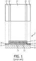
- Fig. 1 shows a cross-section through a prior art multi-device OLED 2.
- the prior art manufacturing process involves applying an anode 22 onto a substrate 20, flanked by but separated from a cathode contact pad 23 and a contact pad 21 for an inter electrode 24.
- These electrically separate regions 21, 22, 23 are shown in the upper part of the diagram as they would appear in a plan view. Only the area covered by the anode 22 will be useful as a light-emitting area of the finished device.
- a first active layer 25 is applied over the anode 22 only.
- An inter electrode 24 is applied onto the active layer 25 and also onto the appropriate contact pad 21.
- a second active layer 27 is deposited over the inter electrode 24.
- This second active layer 27 can have a different colour than the first active layer 25.
- a cathode 26 is applied over the second active layer 27 and onto the cathode contact pad 23.
- the device 2 can be controlled by applying a first voltage across the cathode 26 and the inter electrode 24, and by applying a second voltage across the inter electrode 24 and the anode 22. In this way, the colour of the emitted light can be adjusted or tuned.
- the poor lateral conductivity of the inter electrode 24 and the anode 22 effectively limit the practicable device size.
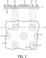
- Fig. 2 shows a schematic representation of a substrate 10 and bottom electrode 11 for a device layer stack 100 of a multi-device OLED according to the invention, and a cross-section A-A' through the substrate 10 and bottom electrode 11.
- the bottom electrode 11 is applied to the substrate 10 using a suitable technique, for example spin coating.
- An island 131 is formed in the electrode 11, for example by performing photolithography or laser ablation to remove material of the bottom electrode 11, leaving an exposed annular region of the substrate 10, as shown in the lower part of the diagram.
- the islands 131 can be very small, for example with a cross-sectional area in the region of 0.7 mm 2 to 1.0 mm 2 (square millimetres).
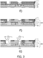
- Fig. 3 shows process steps in the manufacture of a device layer stack 100 of a multi-device OLED according to the invention, using a substrate 10 and bottom electrode 11 prepared in the manner described using Fig. 2 to form a plurality of islands 131.
- a first active layer 120 is applied over the entire surface of the bottom electrode 11, also covering the islands 131 and the exposed annular regions of the substrate 10.
- a laser beam L is used to remove material of the active layer 120 in the region of the island 131, thus exposing the upper surface of the island 131.
- an inter electrode 120 is applied over the entire surface of the layer stack. This inter electrode 120 makes contact with the exposed upper surface of the island 131.
- a laser beam L is used to remove material of the inter electrode 13 and the active layer 120 to expose a region 111 of the upper surface of the bottom electrode 11.
- the area of this exposed bottom electrode region 111 can be in the order of several hundred square micrometers, for example large enough to later accommodate a droplet or globule.
- the size of the exposed area is preferably chosen to comfortably accommodate the droplet with enough space all around the droplet, ensuring that the droplet does not touch any side walls.
- a second active layer 121 is applied over the entire layer stack.
- a top electrode 14 is applied over the entire layer stack.
- laser ablation is performed to re-expose the bottom electrode region 111 and the island 131. In this way, a first opening 110 is formed to access the bottom electrode 11, and a second opening 130 is formed to access the inter electrode 13 using the island 131.
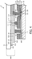
- Fig. 4 shows a device layer stack 100 and a contact layer stack 500 of a multi-device OLED 1 according to the invention.
- the diagram shows how the electrodes 11, 13, 14 of the OLED 1 are connected to current distribution layers 51, 53, 54 in order to apply a voltage across a first OLED device given by the bottom electrode 11, first active layer 120 and inter electrode 13; and to apply a voltage across a second OLED device given by the inter electrode 13, the second active layer 121 and the top electrode 14.
- the connections between the device layer stack 100 and the contact layer stack 500 or multi-polar lid 500 are made by globules 41, 42, 43 of an electrically conductive paste dropped or printed into the openings 110, 130 of the device layer stack 100.
- corresponding vias 510, 530 are formed in the contact layer stack 500 to expose contact regions 511, 531 of the current distribution layers 51, 53.
- a first globule 41 printed into the first opening 110 makes contact with the lowest current distribution layer 54
- a second globule 42 printed into the second opening 130 makes contact with the middle current distribution layer 53 through a via 530 in the contact layer stack 500
- a third globule 43 printed onto the top electrode 14 makes contact with the upper current distribution layer 51 through a via 510 in the contact layer stack 500.
- the gaps between the globules 41, 42, 43 and the conductive materials of the surrounding electrodes 13, 14 and current distribution layers 53, 54 are sufficient to ensure that these cannot be short-circuited.
- the globules can be cured in a curing step to harden the globules and improve the conductivity of the material used.
- the globules can be printed or deposited into the vias of the contact layer stack (instead of into the openings in the device layer stack) if such a curing step would result in damage to the layers of the device layer stack.
- Fig. 5 shows a more realistic (but still exaggerated) cross-section through the device layer stack 100 and the contact layer stack 500 of a multi-device OLED 1 according to the invention.
- the combined thickness of the device layer stack (not including the substrate) can be in the order of 60 nm to 500 nm.
- the contact layer stack 500 or multi-polar cover lid can have a thickness in the order of 50 ⁇ m.
- the electrodes and active layers are indicated by the thin layers on top of the substrate 10, which can be glass or another suitable transparent material.
- the current distribution layers and insulating layers are also simply indicated as thin layers underneath a metal cover lid, which can be some suitable reflective material such as aluminium or silver.
- the globules 41, 42, 43 are shown to connect the appropriate layers.
- Fig. 6 shows a plan view of the light-emitting side of the multi-device OLED 1 of the invention.
- Two power supplies V 1 , V 2 are used to control the OLED devices to tune the colour of the emitted light.
- the light emitting area effectively covers the entire device area. Only those very small areas required by the globules or printed dots to contact the exposed anode regions 111 and the islands 131 will not emit light, since no active layer material is present in these regions 111, 131.
Landscapes
- Physics & Mathematics (AREA)
- Optics & Photonics (AREA)
- Engineering & Computer Science (AREA)
- Manufacturing & Machinery (AREA)
- Electroluminescent Light Sources (AREA)
Claims (11)
- OLED à dispositifs multiples (1) comprenant :- une pile de couches de dispositifs (100) comprenant une électrode inférieure (11) comprenant une région isolée (131), une électrode supérieure (14), au moins une électrode intermédiaire (13) et une pluralité de couches actives (120, 121), dans laquelle l'électrode inférieure (11) est appliquée à un substrat (10), et chaque couche active (120, 121) est enfermée entre deux électrodes (11, 13, 14) ;- un moyen de distribution de courant (500) comprenant une couche de distribution de courant (51, 53, 54) pour chaque électrode (11, 13, 14) de la pile de couches de dispositifs (100) ;- une pluralité d'ouvertures (110, 130) s'étendant de l'électrode supérieure (14) dans la pile de couches de dispositifs (100), dans laquelle chaque ouverture (110, 130) expose une région de contact (111, 131) d'une électrode (11, 13), dans laquelle la région de contact (131) de l'électrode intermédiaire (13) comprend la région isolée (131) de l'électrode inférieure (11), dans laquelle, entre la région isolée (131) de l'électrode inférieure (11) et une partie voisine de l'électrode inférieure (11), une première couche active (120) de la pluralité de couches actives (120, 121) est agencée de manière à être en contact avec la région isolée (131) et la partie voisine de l'électrode inférieure (11), dans laquelle la première couche active (120) est également agencée entre la partie voisine de l'électrode inférieure (11) et l'électrode intermédiaire (13) ; et- une pluralité de connecteurs électriques (41, 42), dans laquelle un connecteur électrique (41, 42) s'étend dans une ouverture (110, 130) pour relier électriquement l'électrode (11, 13) exposée par cette ouverture (110, 130) à la couche de distribution de courant (53, 54) pour cette électrode (11, 13).
- OLED à dispositifs multiples selon la revendication 1, dans laquelle le moyen de distribution de courant (500) comprend une pile de couches de contact (500) avec une pluralité de couches isolantes (520, 521), dans laquelle chaque couche isolante (520, 521) est prise en sandwich entre deux couches de distribution de courant (51, 53, 54).
- OLED à dispositifs multiples selon la revendication 2, dans laquelle le moyen de distribution de courant (500) comprend une pluralité d'interconnexions (510, 530) s'étendant dans la pile de couches de contact (500), dans laquelle chaque interconnexion (510, 530) expose une région de contact (511, 531) d'une couche de distribution de courant (51, 53, 54).
- OLED à dispositifs multiples selon l'une quelconque des revendications précédentes, dans laquelle le moyen de distribution de courant (500) comprend une zone de contact (551, 553, 554) pour chaque couche de distribution de courant (51, 53, 54), dans laquelle chaque zone de contact (551, 553, 554) comprend une portion exposée (551, 553, 554) de cette couche de distribution de courant (51, 53, 54) pour relier cette couche de distribution de courant (51, 53, 54) à une alimentation électrique (V1, V2).
- OLED à dispositifs multiples selon l'une quelconque des revendications précédentes, dans laquelle un connecteur électrique (41, 42, 43) entre une électrode (11, 13, 14) et une couche de distribution de courant (51, 53, 54) comprend un globule (41, 42, 43) de pâte électriquement conductrice placée dans une ouverture (110, 130) et/ou dans une interconnexion (510, 530).
- Procédé de fabrication d'une OLED à dispositifs multiples (1), ledit procédé comprenant les étapes de :- l'assemblage d'une pile de couches de dispositifs (100) comprenant une électrode inférieure (11), une électrode supérieure (14), au moins une électrode intermédiaire (13) et une pluralité de couches actives (120, 121), dans lequel l'électrode inférieure (11) est appliquée à un substrat (10), et chaque couche active (120, 121) est enfermée entre deux électrodes (11, 13, 14), dans lequel l'étape de l'assemblage de la pile de couches de dispositifs (100) comprend les étapes de :- la formation d'une région isolée (131) de l'électrode inférieure (11) ;- l'application d'une première couche active (120) sur l'électrode inférieure (11) pour recouvrir également la région isolée (131), une partie voisine de l'électrode inférieure (11) et une région entre la région isolée (131) et la partie voisine de l'électrode inférieure (11) ;- l'enlèvement d'un matériau de la première couche active (120) pour exposer la région isolée (131) ; et- l'application d'une électrode intermédiaire (13) sur la première couche active (120) pour recouvrir également la région isolée (131) exposée ;- l'assemblage d'un moyen de distribution de courant (500) comprenant une couche de distribution de courant (51, 53, 54) pour chaque électrode (11, 13, 14) de la pile de couches de dispositifs (100) ;- la formation d'une pluralité d'ouvertures (110, 130) s'étendant de l'électrode supérieure (14) dans la pile de couches de dispositifs (100), dans lequel chaque ouverture (110, 130) expose la région de contact (111, 131) de l'électrode intermédiaire (13) ou de l'électrode inférieure (11) ; et- le positionnement d'un connecteur électrique (41, 42), dans chaque ouverture (110, 130) pour relier électriquement l'électrode (11, 13) exposée par cette ouverture (110, 130) à la couche de distribution de courant (53, 54) pour cette électrode (11, 13).
- Procédé selon la revendication 6, dans lequel l'étape de la formation d'une ouverture (110, 130) pour exposer une région de contact (111, 131) d'une électrode (11, 13) comprend l'exécution d'une ablation laser pour enlever un matériau de la pile de couches de dispositifs (100) au-dessus de cette électrode (11, 13).
- Procédé selon la revendication 6 ou 7, dans lequel l'étape de l'assemblage d'un moyen de distribution de courant (500) comprend l'assemblage d'une pile de couches de contact (500), dans lequel des couches de distribution de courant (51, 53, 54) de la pile de couches de contact (500) sont électriquement isolées par une couche isolante (520, 521).
- Procédé selon la revendication 8, comprenant l'étape de la formation d'une interconnexion (510, 530) pour exposer une région de contact (511, 531) d'une couche de distribution de courant (51, 53, 54) de la pile de couches de contact (500).
- Procédé selon la revendication 9, dans lequel une interconnexion (530) est formée dans la pile de couches de contact (500) pour correspondre à une ouverture (130) de la pile de couches de dispositifs (100) de sorte qu'une région exposée (131) d'une électrode (13) repose vis-à-vis d'une région de contact exposée (531) de la couche de distribution de courant (53) pour cette électrode (13) lorsque la pile de couches de contact (500) est placée sur la pile de couches de dispositifs (100).
- Procédé selon l'une quelconque des revendications 6 à 10, dans lequel l'étape du positionnement d'un connecteur électrique (41, 42) comprend l'impression d'un globule (41, 42) de pâte électriquement conductrice sur une région de contact (111, 131) exposée d'une électrode (11, 13).
Priority Applications (1)
| Application Number | Priority Date | Filing Date | Title |
|---|---|---|---|
| EP11773559.7A EP2628182B1 (fr) | 2010-10-11 | 2011-09-29 | Oled à dispositifs multiples |
Applications Claiming Priority (3)
| Application Number | Priority Date | Filing Date | Title |
|---|---|---|---|
| EP10187117 | 2010-10-11 | ||
| EP11773559.7A EP2628182B1 (fr) | 2010-10-11 | 2011-09-29 | Oled à dispositifs multiples |
| PCT/IB2011/054292 WO2012049580A1 (fr) | 2010-10-11 | 2011-09-29 | Oled à dispositifs multiples |
Publications (2)
| Publication Number | Publication Date |
|---|---|
| EP2628182A1 EP2628182A1 (fr) | 2013-08-21 |
| EP2628182B1 true EP2628182B1 (fr) | 2017-03-22 |
Family
ID=44860454
Family Applications (1)
| Application Number | Title | Priority Date | Filing Date |
|---|---|---|---|
| EP11773559.7A Active EP2628182B1 (fr) | 2010-10-11 | 2011-09-29 | Oled à dispositifs multiples |
Country Status (6)
| Country | Link |
|---|---|
| US (1) | US9240563B2 (fr) |
| EP (1) | EP2628182B1 (fr) |
| JP (1) | JP5919282B2 (fr) |
| KR (1) | KR101874889B1 (fr) |
| CN (1) | CN103180954B (fr) |
| WO (1) | WO2012049580A1 (fr) |
Families Citing this family (3)
| Publication number | Priority date | Publication date | Assignee | Title |
|---|---|---|---|---|
| DE102013106815A1 (de) * | 2013-06-28 | 2014-12-31 | Osram Oled Gmbh | Optoelektronisches Bauelement und Verfahren zum Herstellen eines optoelektronischen Bauelementes |
| US9166188B1 (en) * | 2014-06-10 | 2015-10-20 | Arolltech Co., Ltd. | Organic light emitting diode device |
| DE102014112879A1 (de) | 2014-09-08 | 2016-03-10 | Osram Oled Gmbh | Strahlungsemittierende Vorrichtung und Verfahren zur Herstellung derselben |
Citations (2)
| Publication number | Priority date | Publication date | Assignee | Title |
|---|---|---|---|---|
| US20050236981A1 (en) * | 2003-06-11 | 2005-10-27 | Eastman Kodak Company | OLED device |
| WO2006087653A2 (fr) * | 2005-02-16 | 2006-08-24 | Koninklijke Philips Electronics N.V. | Dispositif oled |
Family Cites Families (17)
| Publication number | Priority date | Publication date | Assignee | Title |
|---|---|---|---|---|
| FR2492164B1 (fr) * | 1980-10-15 | 1987-01-23 | Radiotechnique Compelec | Procede de realisation simultanee de liaisons electriques multiples, notamment pour le raccordement electrique d'une micro-plaquette de semiconducteurs |
| US5707745A (en) | 1994-12-13 | 1998-01-13 | The Trustees Of Princeton University | Multicolor organic light emitting devices |
| US5703436A (en) | 1994-12-13 | 1997-12-30 | The Trustees Of Princeton University | Transparent contacts for organic devices |
| US6844957B2 (en) * | 2000-11-29 | 2005-01-18 | International Business Machines Corporation | Three level stacked reflective display |
| JP4310984B2 (ja) * | 2002-02-06 | 2009-08-12 | 株式会社日立製作所 | 有機発光表示装置 |
| JP2004014447A (ja) * | 2002-06-11 | 2004-01-15 | Sony Corp | 表示装置およびその製造方法 |
| US7034470B2 (en) * | 2002-08-07 | 2006-04-25 | Eastman Kodak Company | Serially connecting OLED devices for area illumination |
| JP4574118B2 (ja) * | 2003-02-12 | 2010-11-04 | 株式会社半導体エネルギー研究所 | 半導体装置及びその作製方法 |
| KR100552968B1 (ko) * | 2003-09-23 | 2006-02-15 | 삼성에스디아이 주식회사 | 액티브 매트릭스 유기전계 발광표시장치 |
| US7355204B2 (en) | 2004-12-30 | 2008-04-08 | E.I. Du Pont De Nemours And Company | Organic device with environmental protection structure |
| JP4785447B2 (ja) * | 2005-07-15 | 2011-10-05 | 株式会社半導体エネルギー研究所 | 半導体装置の作製方法 |
| US7855498B2 (en) * | 2005-07-27 | 2010-12-21 | Koninklijke Philips Electronics N.V. | Light-emitting device with a sealing integrated driver circuit |
| JP2009511940A (ja) * | 2005-09-28 | 2009-03-19 | コーニンクレッカ フィリップス エレクトロニクス エヌ ヴィ | 大面積有機ダイオードデバイス及びその製造方法 |
| BRPI0712338A8 (pt) * | 2006-06-07 | 2016-09-27 | Koninklijke Philips Electronics Nv | Dispositivo de iluminação, e, método para fabricar um dispositivo de iluminação |
| WO2008152840A1 (fr) * | 2007-06-13 | 2008-12-18 | Sharp Kabushiki Kaisha | Dispositif d'affichage électroluminescent organique et procédé pour sa fabrication |
| KR101434359B1 (ko) * | 2007-10-08 | 2014-08-26 | 삼성디스플레이 주식회사 | 백색 유기발광소자 |
| EP2144290A1 (fr) | 2008-07-08 | 2010-01-13 | Nederlandse Organisatie voor toegepast- natuurwetenschappelijk onderzoek TNO | Dispositif électronique et son procédé de fabrication |
-
2011
- 2011-09-29 US US13/877,665 patent/US9240563B2/en active Active
- 2011-09-29 CN CN201180049226.5A patent/CN103180954B/zh active Active
- 2011-09-29 WO PCT/IB2011/054292 patent/WO2012049580A1/fr active Application Filing
- 2011-09-29 EP EP11773559.7A patent/EP2628182B1/fr active Active
- 2011-09-29 KR KR1020137012225A patent/KR101874889B1/ko active IP Right Grant
- 2011-09-29 JP JP2013532297A patent/JP5919282B2/ja active Active
Patent Citations (2)
| Publication number | Priority date | Publication date | Assignee | Title |
|---|---|---|---|---|
| US20050236981A1 (en) * | 2003-06-11 | 2005-10-27 | Eastman Kodak Company | OLED device |
| WO2006087653A2 (fr) * | 2005-02-16 | 2006-08-24 | Koninklijke Philips Electronics N.V. | Dispositif oled |
Also Published As
| Publication number | Publication date |
|---|---|
| KR20130119440A (ko) | 2013-10-31 |
| CN103180954A (zh) | 2013-06-26 |
| US20130187148A1 (en) | 2013-07-25 |
| WO2012049580A1 (fr) | 2012-04-19 |
| KR101874889B1 (ko) | 2018-07-06 |
| CN103180954B (zh) | 2017-02-22 |
| EP2628182A1 (fr) | 2013-08-21 |
| JP2013542564A (ja) | 2013-11-21 |
| US9240563B2 (en) | 2016-01-19 |
| JP5919282B2 (ja) | 2016-05-18 |
Similar Documents
| Publication | Publication Date | Title |
|---|---|---|
| US9048450B2 (en) | OLED device with a brightness distribution controlling means | |
| CN110853531B (zh) | 显示用驱动背板及其制备方法、显示面板 | |
| JP2013544009A5 (fr) | ||
| KR20100023897A (ko) | 어드레스 가능 및 정적 전자 디스플레이, 발전 및 다른 전자 장치를 제조하는 방법 | |
| EP2628182B1 (fr) | Oled à dispositifs multiples | |
| US9379349B2 (en) | OLED device with spatially isolated light-emitting areas | |
| TWI557898B (zh) | 有機發光二極體陣列 | |
| CN111162162A (zh) | 转移基板及其制备方法、微发光二极管的转移方法 | |
| TWI545822B (zh) | 有機發光二極體陣列的製備方法 | |
| CN110752209B (zh) | 一种显示用驱动背板及其制备方法、显示面板 | |
| CN102652371A (zh) | 用于创建串联连接的oled器件的方法 | |
| TWI566386B (zh) | 有機發光二極體陣列 | |
| TW201530751A (zh) | 有機發光二極體陣列的製備方法 | |
| WO2011083414A1 (fr) | Procédé de fabrication d'un dispositif oled | |
| WO2011101766A1 (fr) | Dispositif oled et procédé de fabrication associé | |
| CN113035854A (zh) | 集成芯片及其制造方法、全彩集成芯片和显示面板 | |
| EP3231256B1 (fr) | Éléments électroluminescents et procédés de construction | |
| TWI545829B (zh) | 有機發光二極體陣列的製備方法 | |
| JP2005142118A (ja) | 基板装置の製造方法 | |
| JP2022530448A (ja) | Ledモジュール、ledディスプレイモジュール、および当該モジュールを製造する方法 |
Legal Events
| Date | Code | Title | Description |
|---|---|---|---|
| PUAI | Public reference made under article 153(3) epc to a published international application that has entered the european phase |
Free format text: ORIGINAL CODE: 0009012 |
|
| 17P | Request for examination filed |
Effective date: 20130513 |
|
| AK | Designated contracting states |
Kind code of ref document: A1 Designated state(s): AL AT BE BG CH CY CZ DE DK EE ES FI FR GB GR HR HU IE IS IT LI LT LU LV MC MK MT NL NO PL PT RO RS SE SI SK SM TR |
|
| RAP1 | Party data changed (applicant data changed or rights of an application transferred) |
Owner name: KONINKLIJKE PHILIPS N.V. Owner name: PHILIPS INTELLECTUAL PROPERTY & STANDARDS GMBH |
|
| DAX | Request for extension of the european patent (deleted) | ||
| 17Q | First examination report despatched |
Effective date: 20150107 |
|
| GRAP | Despatch of communication of intention to grant a patent |
Free format text: ORIGINAL CODE: EPIDOSNIGR1 |
|
| INTG | Intention to grant announced |
Effective date: 20161011 |
|
| GRAS | Grant fee paid |
Free format text: ORIGINAL CODE: EPIDOSNIGR3 |
|
| GRAA | (expected) grant |
Free format text: ORIGINAL CODE: 0009210 |
|
| AK | Designated contracting states |
Kind code of ref document: B1 Designated state(s): AL AT BE BG CH CY CZ DE DK EE ES FI FR GB GR HR HU IE IS IT LI LT LU LV MC MK MT NL NO PL PT RO RS SE SI SK SM TR |
|
| REG | Reference to a national code |
Ref country code: GB Ref legal event code: FG4D |
|
| REG | Reference to a national code |
Ref country code: CH Ref legal event code: EP |
|
| REG | Reference to a national code |
Ref country code: AT Ref legal event code: REF Ref document number: 878539 Country of ref document: AT Kind code of ref document: T Effective date: 20170415 |
|
| REG | Reference to a national code |
Ref country code: IE Ref legal event code: FG4D |
|
| REG | Reference to a national code |
Ref country code: DE Ref legal event code: R096 Ref document number: 602011036257 Country of ref document: DE |
|
| REG | Reference to a national code |
Ref country code: NL Ref legal event code: MP Effective date: 20170322 |
|
| PG25 | Lapsed in a contracting state [announced via postgrant information from national office to epo] |
Ref country code: GR Free format text: LAPSE BECAUSE OF FAILURE TO SUBMIT A TRANSLATION OF THE DESCRIPTION OR TO PAY THE FEE WITHIN THE PRESCRIBED TIME-LIMIT Effective date: 20170623 Ref country code: HR Free format text: LAPSE BECAUSE OF FAILURE TO SUBMIT A TRANSLATION OF THE DESCRIPTION OR TO PAY THE FEE WITHIN THE PRESCRIBED TIME-LIMIT Effective date: 20170322 Ref country code: FI Free format text: LAPSE BECAUSE OF FAILURE TO SUBMIT A TRANSLATION OF THE DESCRIPTION OR TO PAY THE FEE WITHIN THE PRESCRIBED TIME-LIMIT Effective date: 20170322 Ref country code: LT Free format text: LAPSE BECAUSE OF FAILURE TO SUBMIT A TRANSLATION OF THE DESCRIPTION OR TO PAY THE FEE WITHIN THE PRESCRIBED TIME-LIMIT Effective date: 20170322 Ref country code: NO Free format text: LAPSE BECAUSE OF FAILURE TO SUBMIT A TRANSLATION OF THE DESCRIPTION OR TO PAY THE FEE WITHIN THE PRESCRIBED TIME-LIMIT Effective date: 20170622 |
|
| REG | Reference to a national code |
Ref country code: LT Ref legal event code: MG4D |
|
| REG | Reference to a national code |
Ref country code: AT Ref legal event code: MK05 Ref document number: 878539 Country of ref document: AT Kind code of ref document: T Effective date: 20170322 |
|
| PG25 | Lapsed in a contracting state [announced via postgrant information from national office to epo] |
Ref country code: BG Free format text: LAPSE BECAUSE OF FAILURE TO SUBMIT A TRANSLATION OF THE DESCRIPTION OR TO PAY THE FEE WITHIN THE PRESCRIBED TIME-LIMIT Effective date: 20170622 Ref country code: SE Free format text: LAPSE BECAUSE OF FAILURE TO SUBMIT A TRANSLATION OF THE DESCRIPTION OR TO PAY THE FEE WITHIN THE PRESCRIBED TIME-LIMIT Effective date: 20170322 Ref country code: LV Free format text: LAPSE BECAUSE OF FAILURE TO SUBMIT A TRANSLATION OF THE DESCRIPTION OR TO PAY THE FEE WITHIN THE PRESCRIBED TIME-LIMIT Effective date: 20170322 Ref country code: RS Free format text: LAPSE BECAUSE OF FAILURE TO SUBMIT A TRANSLATION OF THE DESCRIPTION OR TO PAY THE FEE WITHIN THE PRESCRIBED TIME-LIMIT Effective date: 20170322 |
|
| REG | Reference to a national code |
Ref country code: FR Ref legal event code: PLFP Year of fee payment: 7 |
|
| PG25 | Lapsed in a contracting state [announced via postgrant information from national office to epo] |
Ref country code: NL Free format text: LAPSE BECAUSE OF FAILURE TO SUBMIT A TRANSLATION OF THE DESCRIPTION OR TO PAY THE FEE WITHIN THE PRESCRIBED TIME-LIMIT Effective date: 20170322 |
|
| PG25 | Lapsed in a contracting state [announced via postgrant information from national office to epo] |
Ref country code: EE Free format text: LAPSE BECAUSE OF FAILURE TO SUBMIT A TRANSLATION OF THE DESCRIPTION OR TO PAY THE FEE WITHIN THE PRESCRIBED TIME-LIMIT Effective date: 20170322 Ref country code: ES Free format text: LAPSE BECAUSE OF FAILURE TO SUBMIT A TRANSLATION OF THE DESCRIPTION OR TO PAY THE FEE WITHIN THE PRESCRIBED TIME-LIMIT Effective date: 20170322 Ref country code: SK Free format text: LAPSE BECAUSE OF FAILURE TO SUBMIT A TRANSLATION OF THE DESCRIPTION OR TO PAY THE FEE WITHIN THE PRESCRIBED TIME-LIMIT Effective date: 20170322 Ref country code: IT Free format text: LAPSE BECAUSE OF FAILURE TO SUBMIT A TRANSLATION OF THE DESCRIPTION OR TO PAY THE FEE WITHIN THE PRESCRIBED TIME-LIMIT Effective date: 20170322 Ref country code: CZ Free format text: LAPSE BECAUSE OF FAILURE TO SUBMIT A TRANSLATION OF THE DESCRIPTION OR TO PAY THE FEE WITHIN THE PRESCRIBED TIME-LIMIT Effective date: 20170322 Ref country code: AT Free format text: LAPSE BECAUSE OF FAILURE TO SUBMIT A TRANSLATION OF THE DESCRIPTION OR TO PAY THE FEE WITHIN THE PRESCRIBED TIME-LIMIT Effective date: 20170322 Ref country code: RO Free format text: LAPSE BECAUSE OF FAILURE TO SUBMIT A TRANSLATION OF THE DESCRIPTION OR TO PAY THE FEE WITHIN THE PRESCRIBED TIME-LIMIT Effective date: 20170322 |
|
| PG25 | Lapsed in a contracting state [announced via postgrant information from national office to epo] |
Ref country code: PT Free format text: LAPSE BECAUSE OF FAILURE TO SUBMIT A TRANSLATION OF THE DESCRIPTION OR TO PAY THE FEE WITHIN THE PRESCRIBED TIME-LIMIT Effective date: 20170724 Ref country code: PL Free format text: LAPSE BECAUSE OF FAILURE TO SUBMIT A TRANSLATION OF THE DESCRIPTION OR TO PAY THE FEE WITHIN THE PRESCRIBED TIME-LIMIT Effective date: 20170322 Ref country code: SM Free format text: LAPSE BECAUSE OF FAILURE TO SUBMIT A TRANSLATION OF THE DESCRIPTION OR TO PAY THE FEE WITHIN THE PRESCRIBED TIME-LIMIT Effective date: 20170322 Ref country code: IS Free format text: LAPSE BECAUSE OF FAILURE TO SUBMIT A TRANSLATION OF THE DESCRIPTION OR TO PAY THE FEE WITHIN THE PRESCRIBED TIME-LIMIT Effective date: 20170722 |
|
| PGFP | Annual fee paid to national office [announced via postgrant information from national office to epo] |
Ref country code: TR Payment date: 20170920 Year of fee payment: 7 |
|
| REG | Reference to a national code |
Ref country code: DE Ref legal event code: R097 Ref document number: 602011036257 Country of ref document: DE |
|
| PLBE | No opposition filed within time limit |
Free format text: ORIGINAL CODE: 0009261 |
|
| STAA | Information on the status of an ep patent application or granted ep patent |
Free format text: STATUS: NO OPPOSITION FILED WITHIN TIME LIMIT |
|
| PG25 | Lapsed in a contracting state [announced via postgrant information from national office to epo] |
Ref country code: DK Free format text: LAPSE BECAUSE OF FAILURE TO SUBMIT A TRANSLATION OF THE DESCRIPTION OR TO PAY THE FEE WITHIN THE PRESCRIBED TIME-LIMIT Effective date: 20170322 |
|
| REG | Reference to a national code |
Ref country code: DE Ref legal event code: R082 Ref document number: 602011036257 Country of ref document: DE Representative=s name: DOMPATENT VON KREISLER SELTING WERNER - PARTNE, DE Ref country code: DE Ref legal event code: R082 Ref document number: 602011036257 Country of ref document: DE Ref country code: DE Ref legal event code: R081 Ref document number: 602011036257 Country of ref document: DE Owner name: BEIJING XIAOMI MOBILE SOFTWARE CO., LTD., CN Free format text: FORMER OWNER: PHILIPS INTELLECTUAL PROPERTY & STANDARDS GMBH, 20099 HAMBURG, DE Ref country code: DE Ref legal event code: R081 Ref document number: 602011036257 Country of ref document: DE Owner name: PHILIPS GMBH, DE Free format text: FORMER OWNER: PHILIPS INTELLECTUAL PROPERTY & STANDARDS GMBH, 20099 HAMBURG, DE |
|
| 26N | No opposition filed |
Effective date: 20180102 |
|
| PG25 | Lapsed in a contracting state [announced via postgrant information from national office to epo] |
Ref country code: SI Free format text: LAPSE BECAUSE OF FAILURE TO SUBMIT A TRANSLATION OF THE DESCRIPTION OR TO PAY THE FEE WITHIN THE PRESCRIBED TIME-LIMIT Effective date: 20170322 |
|
| REG | Reference to a national code |
Ref country code: CH Ref legal event code: PL |
|
| PG25 | Lapsed in a contracting state [announced via postgrant information from national office to epo] |
Ref country code: MC Free format text: LAPSE BECAUSE OF FAILURE TO SUBMIT A TRANSLATION OF THE DESCRIPTION OR TO PAY THE FEE WITHIN THE PRESCRIBED TIME-LIMIT Effective date: 20170322 |
|
| REG | Reference to a national code |
Ref country code: DE Ref legal event code: R082 Ref document number: 602011036257 Country of ref document: DE Representative=s name: DOMPATENT VON KREISLER SELTING WERNER - PARTNE, DE |
|
| REG | Reference to a national code |
Ref country code: IE Ref legal event code: MM4A |
|
| REG | Reference to a national code |
Ref country code: BE Ref legal event code: MM Effective date: 20170930 |
|
| PG25 | Lapsed in a contracting state [announced via postgrant information from national office to epo] |
Ref country code: LU Free format text: LAPSE BECAUSE OF NON-PAYMENT OF DUE FEES Effective date: 20170929 |
|
| PG25 | Lapsed in a contracting state [announced via postgrant information from national office to epo] |
Ref country code: LI Free format text: LAPSE BECAUSE OF NON-PAYMENT OF DUE FEES Effective date: 20170930 Ref country code: CH Free format text: LAPSE BECAUSE OF NON-PAYMENT OF DUE FEES Effective date: 20170930 Ref country code: IE Free format text: LAPSE BECAUSE OF NON-PAYMENT OF DUE FEES Effective date: 20170929 |
|
| PG25 | Lapsed in a contracting state [announced via postgrant information from national office to epo] |
Ref country code: BE Free format text: LAPSE BECAUSE OF NON-PAYMENT OF DUE FEES Effective date: 20170930 |
|
| REG | Reference to a national code |
Ref country code: GB Ref legal event code: 732E Free format text: REGISTERED BETWEEN 20180809 AND 20180815 |
|
| REG | Reference to a national code |
Ref country code: FR Ref legal event code: PLFP Year of fee payment: 8 |
|
| PG25 | Lapsed in a contracting state [announced via postgrant information from national office to epo] |
Ref country code: MT Free format text: LAPSE BECAUSE OF NON-PAYMENT OF DUE FEES Effective date: 20170929 |
|
| PG25 | Lapsed in a contracting state [announced via postgrant information from national office to epo] |
Ref country code: HU Free format text: LAPSE BECAUSE OF FAILURE TO SUBMIT A TRANSLATION OF THE DESCRIPTION OR TO PAY THE FEE WITHIN THE PRESCRIBED TIME-LIMIT; INVALID AB INITIO Effective date: 20110929 |
|
| REG | Reference to a national code |
Ref country code: DE Ref legal event code: R082 Ref document number: 602011036257 Country of ref document: DE Representative=s name: DOMPATENT VON KREISLER SELTING WERNER - PARTNE, DE Ref country code: DE Ref legal event code: R081 Ref document number: 602011036257 Country of ref document: DE Owner name: BEIJING XIAOMI MOBILE SOFTWARE CO., LTD., CN Free format text: FORMER OWNER: PHILIPS GMBH, 22335 HAMBURG, DE |
|
| PG25 | Lapsed in a contracting state [announced via postgrant information from national office to epo] |
Ref country code: CY Free format text: LAPSE BECAUSE OF NON-PAYMENT OF DUE FEES Effective date: 20170322 |
|
| PG25 | Lapsed in a contracting state [announced via postgrant information from national office to epo] |
Ref country code: MK Free format text: LAPSE BECAUSE OF FAILURE TO SUBMIT A TRANSLATION OF THE DESCRIPTION OR TO PAY THE FEE WITHIN THE PRESCRIBED TIME-LIMIT Effective date: 20170322 |
|
| PG25 | Lapsed in a contracting state [announced via postgrant information from national office to epo] |
Ref country code: AL Free format text: LAPSE BECAUSE OF FAILURE TO SUBMIT A TRANSLATION OF THE DESCRIPTION OR TO PAY THE FEE WITHIN THE PRESCRIBED TIME-LIMIT Effective date: 20170322 |
|
| PG25 | Lapsed in a contracting state [announced via postgrant information from national office to epo] |
Ref country code: TR Free format text: LAPSE BECAUSE OF NON-PAYMENT OF DUE FEES Effective date: 20180929 |
|
| REG | Reference to a national code |
Ref country code: DE Ref legal event code: R079 Ref document number: 602011036257 Country of ref document: DE Free format text: PREVIOUS MAIN CLASS: H01L0027320000 Ipc: H10K0059000000 |
|
| P01 | Opt-out of the competence of the unified patent court (upc) registered |
Effective date: 20230531 |
|
| PGFP | Annual fee paid to national office [announced via postgrant information from national office to epo] |
Ref country code: GB Payment date: 20230920 Year of fee payment: 13 |
|
| PGFP | Annual fee paid to national office [announced via postgrant information from national office to epo] |
Ref country code: FR Payment date: 20230928 Year of fee payment: 13 Ref country code: DE Payment date: 20230920 Year of fee payment: 13 |