EP2626904A2 - Organic light emitting diode display - Google Patents
Organic light emitting diode display Download PDFInfo
- Publication number
- EP2626904A2 EP2626904A2 EP13154642.6A EP13154642A EP2626904A2 EP 2626904 A2 EP2626904 A2 EP 2626904A2 EP 13154642 A EP13154642 A EP 13154642A EP 2626904 A2 EP2626904 A2 EP 2626904A2
- Authority
- EP
- European Patent Office
- Prior art keywords
- thin film
- film transistor
- insulation layer
- light emitting
- emitting diode
- Prior art date
- Legal status (The legal status is an assumption and is not a legal conclusion. Google has not performed a legal analysis and makes no representation as to the accuracy of the status listed.)
- Withdrawn
Links
- 238000009413 insulation Methods 0.000 claims abstract description 121
- 239000000758 substrate Substances 0.000 claims abstract description 31
- 239000010409 thin film Substances 0.000 claims description 189
- 239000003990 capacitor Substances 0.000 claims description 121
- 239000010410 layer Substances 0.000 description 185
- 239000000463 material Substances 0.000 description 8
- 229910021420 polycrystalline silicon Inorganic materials 0.000 description 8
- 229920005591 polysilicon Polymers 0.000 description 8
- 239000010408 film Substances 0.000 description 4
- 230000008859 change Effects 0.000 description 3
- 239000000470 constituent Substances 0.000 description 2
- 230000008878 coupling Effects 0.000 description 2
- 238000010168 coupling process Methods 0.000 description 2
- 238000005859 coupling reaction Methods 0.000 description 2
- 230000006866 deterioration Effects 0.000 description 2
- 238000010586 diagram Methods 0.000 description 2
- 230000000694 effects Effects 0.000 description 2
- 241001270131 Agaricus moelleri Species 0.000 description 1
- 230000003247 decreasing effect Effects 0.000 description 1
- 238000005516 engineering process Methods 0.000 description 1
- 230000007717 exclusion Effects 0.000 description 1
- 230000005484 gravity Effects 0.000 description 1
- 238000005286 illumination Methods 0.000 description 1
- 230000001788 irregular Effects 0.000 description 1
- 239000004973 liquid crystal related substance Substances 0.000 description 1
- 239000011159 matrix material Substances 0.000 description 1
- 230000004048 modification Effects 0.000 description 1
- 238000012986 modification Methods 0.000 description 1
- 230000004044 response Effects 0.000 description 1
- 239000002356 single layer Substances 0.000 description 1
- 230000009466 transformation Effects 0.000 description 1
Images



Classifications
-
- H—ELECTRICITY
- H10—SEMICONDUCTOR DEVICES; ELECTRIC SOLID-STATE DEVICES NOT OTHERWISE PROVIDED FOR
- H10K—ORGANIC ELECTRIC SOLID-STATE DEVICES
- H10K59/00—Integrated devices, or assemblies of multiple devices, comprising at least one organic light-emitting element covered by group H10K50/00
- H10K59/10—OLED displays
- H10K59/12—Active-matrix OLED [AMOLED] displays
- H10K59/131—Interconnections, e.g. wiring lines or terminals
-
- H—ELECTRICITY
- H10—SEMICONDUCTOR DEVICES; ELECTRIC SOLID-STATE DEVICES NOT OTHERWISE PROVIDED FOR
- H10D—INORGANIC ELECTRIC SEMICONDUCTOR DEVICES
- H10D84/00—Integrated devices formed in or on semiconductor substrates that comprise only semiconducting layers, e.g. on Si wafers or on GaAs-on-Si wafers
- H10D84/90—Masterslice integrated circuits
- H10D84/903—Masterslice integrated circuits comprising field effect technology
- H10D84/907—CMOS gate arrays
- H10D84/968—Macro-architecture
- H10D84/974—Layout specifications, i.e. inner core regions
- H10D84/979—Data lines, e.g. buses
-
- H—ELECTRICITY
- H10—SEMICONDUCTOR DEVICES; ELECTRIC SOLID-STATE DEVICES NOT OTHERWISE PROVIDED FOR
- H10K—ORGANIC ELECTRIC SOLID-STATE DEVICES
- H10K30/00—Organic devices sensitive to infrared radiation, light, electromagnetic radiation of shorter wavelength or corpuscular radiation
- H10K30/80—Constructional details
- H10K30/865—Intermediate layers comprising a mixture of materials of the adjoining active layers
Definitions
- the present invention relates generally to an organic light emitting diode (OLED) display. More particularly, the invention relates generally to an organic light emitting diode (OLED) display including a pixel circuit having a plurality of thin film transistors and at least one capacitor.
- a display device is a device for displaying images, and recently, a display device including an organic light emitting diode (OLED) has come to prominence.
- OLED organic light emitting diode
- the OLED Unlike a liquid crystal display (LCD), the OLED has the characteristic of self-emission and does not require a light source, so the thickness and weight of an overall display device can be reduced.
- the OLED exhibits high quality characteristics such as low power consumption, high luminance, and a high response speed.
- the organic light emitting diode (OLED) display includes gate wires provided on a substrate and extended in a direction, data wires extended to cross the gate wires, a pixel circuit connected to the gate wires and the data wires, and an organic light emitting diode connected to the pixel circuit.
- the present invention sets out to provide a high-resolution organic light emitting diode (OLED) display for improving display quality.
- OLED organic light emitting diode
- An embodiment of the invention provides an organic light emitting diode display including: a first insulation layer formed over a substrate; a plurality of first gate wires, extended in a first direction, provided on the first insulation layer; a second insulation layer formed over the plurality of first gate wires and the first insulation layer; a plurality of second gate wires, extended in the first direction, provided on the second insulation layer; a third insulation layer formed over the plurality of second gate wires and the second insulation layer; a plurality of data wires, extended in a second direction crossing the first direction provided, provided on the third insulation layer; a pixel circuit connected to the first gate wires, the second gate wires, and the data wires; and an organic light emitting diode connected to the pixel circuit.
- the first gate wires need not be overlapped by the second gate wires.
- the second gate wires may include a first scan line and a reset power line separated from the first scan line, the first gate wires may include a second scan line and a light emission control line, and the data wires include a data line and a drive power line separated from the data line.
- the pixel circuit may include: a first capacitor connected to the reset power line and the drive power line; a first thin film transistor connected between the drive power line and the organic light emitting diode; and a second thin film transistor connected between the data line and the first thin film transistor.
- the first capacitor may include: a first capacitor connected to the reset power line and the drive power line; a first thin film transistor connected between the drive power line and the organic light emitting diode; and a second thin film transistor connected between the data line and the first thin film transistor.
- the first capacitor may include: a first capacitor electrode formed on the first insulation layer and connected to the reset power line; and a second capacitor electrode formed on the second insulation layer and connected to the drive power line.
- the first capacitor may include an active electrode connected to the second capacitor electrode, and the active electrode is provided between the substrate and the first insulation layer corresponding to the first capacitor electrode.
- the second capacitor electrode may be extended in the first direction.
- the first thin film transistor may include: a first active layer, the first insulation layer being formed over the first active layer; a first gate electrode connected to the first capacitor electrode and provided on the second insulation layer; a first source electrode connected to the drive power line; and a first drain electrode connected to the organic light emitting diode.
- the second thin film transistor may include: a second active layer, the first insulation layer being formed over the second active layer; a second gate electrode connected to the first scan line and provided on the first insulation layer; a second source electrode connected to the data line; and a second drain electrode connected to the first source electrode of the first thin film transistor.
- the second thin film transistor may include: a second active layer, the first insulation layer being formed over the second active layer; a second gate electrode connected to the first scan line and provided on the second insulation layer; a second source electrode connected to the data line; and a second drain electrode connected to the first source electrode of the first thin film transistor.
- the pixel circuit may further include a second capacitor including a third capacitor electrode formed on the first insulation layer and connected to the first capacitor electrode, and a fourth capacitor electrode formed on the second insulation layer and connected to the first scan line.
- the pixel circuit may further include a third thin film transistor including a third active layer provided between the substrate and the first insulation layer, a third gate electrode connected to the first scan line and provided on the second insulation layer, a third source electrode connected to the first drain electrode of the first thin film transistor, and a third drain electrode connected to the first gate electrode of the first thin film transistor.
- a third thin film transistor including a third active layer provided between the substrate and the first insulation layer, a third gate electrode connected to the first scan line and provided on the second insulation layer, a third source electrode connected to the first drain electrode of the first thin film transistor, and a third drain electrode connected to the first gate electrode of the first thin film transistor.
- the first gate wires may include a second scan line
- the pixel circuit further includes a fourth thin film transistor including a fourth active layer provided between the substrate and the first insulation layer, a fourth gate electrode connected to the second scan line and provided on the first insulation layer, a fourth source electrode connected to the reset power line, and a fourth drain electrode connected to the first gate electrode of the first thin film transistor.
- the first gate wires may further include a light emission control line
- the pixel circuit may further include a fifth thin film transistor including a fifth active layer provided between the substrate and the first insulation layer, a fifth gate electrode connected to the light emission control line and provided on the first insulation layer, a fifth source electrode connected to the drive power line, and a fifth drain electrode connected to the first source electrode of the first thin film transistor.
- the pixel circuit may further include a sixth thin film transistor including a sixth active layer provided between the substrate and the first insulation layer, a sixth gate electrode connected to the light emission control line and provided on the first insulation layer, a sixth source electrode connected to the first drain electrode of the first thin film transistor, and a sixth drain electrode connected to the organic light emitting diode.
- a sixth thin film transistor including a sixth active layer provided between the substrate and the first insulation layer, a sixth gate electrode connected to the light emission control line and provided on the first insulation layer, a sixth source electrode connected to the first drain electrode of the first thin film transistor, and a sixth drain electrode connected to the organic light emitting diode.
- an organic light emitting diode display including: a first insulation layer formed over a substrate; a plurality of first gate wires, extended in a first direction, provided on the first insulation layer; a second insulation layer formed over the plurality of first gate wires and the first insulation layer; a plurality of second gate wires, extended in the first direction, provided on the second insulation layer; a third insulation layer formed over the plurality of second gate wires and the second insulation layer; a plurality of data wires, extended in a second direction crossing the first direction provided, provided on the third insulation layer; a pixel circuit including a plurality of thin film transistors and at least one capacitor connected to the first gate wires, the second gate wires, and the data wires; and an organic light emitting diode connected to a first power via the pixel circuit and further connected to a second power.
- a gate electrode of a drive thin film transistor having a source electrode connected to the first power and a drain electrode connected to the organic light emitting diode, from among the plurality of thin film transistors, may be provided on the second insulation layer.
- a gate electrode of a compensation thin film transistor having a source electrode connected to the drain electrode of the drive thin film transistor and a drain electrode connected to the gate electrode of the drive thin film transistor, from among the plurality of thin film transistors, may be provided on the second insulation layer.
- a gate electrode of at least one switching thin film transistor, separate from the drive thin film transistor and the compensation thin film transistor, from among the plurality of thin film transistors may be provided on the first insulation layer.
- a first electrode of the capacitor is provided on the first insulation layer, and a second electrode of the capacitor, facing the first electrode, may be provided on the second insulation layer.
- embodiments of the invention can provide a, high-resolution organic light emitting diode (OLED) display with improved display quality.
- OLED organic light emitting diode
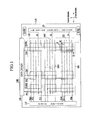
- FIG. 1 illustrates an organic light emitting diode (OLED) display according to a first embodiment of the invention
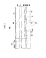
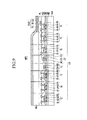
- FIG. 2 is a cross-sectional view with respect to a line II-II shown in FIG. 1 ;
- FIG. 3 is a circuit diagram of a pixel shown in FIG. 1 ;
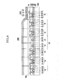
- FIG. 4 is a cross-sectional view of a pixel circuit and an organic light emitting diode shown in FIG. 3 ;
- FIG. 5 to FIG. 7 are graphs for describing effects of an organic light emitting diode (OLED) display according to a first embodiment of the invention
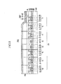
- FIG. 8 is a cross-sectional view of a pixel circuit and an organic light emitting diode of an organic light emitting diode (OLED) display according to a second embodiment of the invention.
- FIG. 9 is a cross-sectional view of a pixel circuit and an organic light emitting diode of an organic light emitting diode (OLED) display according to a third embodiment of the invention.
- the attached drawings illustrate an active matrix (AM) display device having a 6Tr-2Cap structure in which a pixel has six thin film transistors (TFTs) and two capacitors, but the present invention is not limited thereto. Therefore, the organic light emitting diode (OLED) display can include a plurality of thin film transistors and at least one capacitor for each pixel, and can further have an additional wire or omit existing wires for various configurations.
- the pixel represents a minimum unit for displaying an image, and the organic light emitting diode (OLED) display expresses the image through a plurality of pixels.
- OLED organic light emitting diode
- the organic light emitting diode (OLED) display 1000 includes a gate driver 110, first gate wires GW1, second gate wires GW2, a light emission control driver 120, a data driver 130, data wires (DW), a display 140, and pixels 150.
- the gate driver 110 sequentially supplies a scan signal to first scan lines (SC2-SCn) or second scan lines (SC1-SCn-1) included in first gate wires GW1 or second gate wires GW2 according to a control signal provided by an external circuit (not shown), for example, a timing controller.
- Each pixel 150 is selected by a scan signal and sequentially receives data signals.
- the first gate wires GW1 are provided on a substrate (SUB), with a buffer layer (BU) and a first insulation layer GI1 therebetween, and are extended in a first direction.
- the first gate wires GW1 include the second scan line (SCn-1) and light emission control line (En).
- the second scan line (SCn-1) is connected to the gate driver 110 and receives a scan signal from the gate driver 110.
- the light emission control line (En) is connected to the light emission control driver 120 and receives a light emission control signal from the light emission control driver 120.
- the second gate wires GW2 are provided in a separate layer above the first gate wires GW1, with a second insulation layer GI2 therebetween, and are extended in the first direction.
- the second gate wires GW2 do not overlap the first gate wires GW1.
- the second gate wires GW2 include the first scan line (SCn) and a reset power line (Vinit).
- the first scan line (SCn) is connected to the gate driver 110 and receives the scan signal from the gate driver 110.
- the reset power line (Vinit) is connected to the gate driver 110 and receives a reset power from the gate driver 110.
- the reset power line (Vinit) is described to receive the reset power from the gate driver 110 in this first embodiment, and the reset power line (Vinit) can also be connected to another additional component to receive the reset power therefrom according to another embodiment.
- the light emission control driver 120 sequentially supplies a light emission control signal to the light emission control lines (E1-En) corresponding to a control signal supplied by an external device such as a timing controller. Emission of light by the pixel 150 is then controlled by the light emission control signal. That is, the light emission control signal controls a light emitting time of the pixel 150.
- the light emission control driver 120 can be omitted depending on an internal configuration of the pixel 150.
- the data driver 130 supplies a data signal to the data line (DAm) from among the data wires (DW) corresponding to a control signal provided by an external device such as a timing controller.
- the data signal supplied to the data line (DAm) is supplied as a pixel 150 selected by the scan signal each time the scan signal is supplied to the first scan line (SCn).
- the pixel 150 is charged with a voltage that corresponds to the data signal, and emits light with corresponding luminance.
- the data wires (DW) are provided in a separate layer above the second gate wires GW2, with a third insulation layer (ILD) therebetween, and are extended in a second direction crossing the first direction.
- the data wires (DW) include data lines (DA1-DAm) and a drive power line (ELVDDL).
- the data line (DAm) is connected to the data driver 130 and receives the data signal from the data driver 130.
- the drive power line (ELVDDL) is connected to a first power (ELVDD) and receives a drive power from the first power (ELVDD).
- the first power (ELVDD) may be external.
- the display 140 includes a plurality of pixels 150 provided at areas where the first gate wires GW1, the second gate wires GW2, and the data wires (DW) cross.
- the pixel 150 includes an organic light emitting diode for emitting light with luminance that corresponds to the driving current that corresponds to the data signal, and a pixel circuit ( FIG. 3 ) for controlling the driving current flowing to the organic light emitting diode.
- the pixel circuit is connected to the first gate wires GW1, the second gate wires GW2, and the data wires DW, and the organic light emitting diode is connected to the pixel circuit.
- the organic light emitting diode of the display 140 is connected to the first power (ELVDD) with the pixel circuit therebetween, and it is connected to a second power (ELVSS), which may also be external.
- the first power (ELVDD) and the second power (ELVSS) supply drive power and common power to the pixel 150 of the display 140, and the pixel 150 emits light with the luminance that corresponds to the driving current passing through the organic light emitting diode from the first power (ELVDD) corresponding to the data signal according to the drive power and the common power supplied to the pixel 150.
- the first gate wires GW1 include the second scan line (SCn-1) and light emission control line (En) provided on the same layer that cross the pixel 150 in the first direction and that are not overlapped with each other
- the second gate wires GW2 include the first scan line (SCn) and the reset power line (Vinit) provided on the same layer that cross the pixel 150 in the first direction and that are not overlapped with each other, but the first gate wires GW1 and the second gate wires GW2 are provided on different layers with the second insulation layer GI2 therebetween.
- a distance (W) between the neighboring gate wires provided on different layers and a greater number of pixels 150 can be formed in the same area. That is, the high-resolution organic light emitting diode (OLED) display 1000 can be formed.
- a second capacitor electrode CE2 represents an electrode for configuring a first capacitor C1 ( FIG. 3 ), and when the second capacitor electrode CE2 is extended in the first direction if needed, the second capacitor electrode CE2 is formed on the same layer as the second gate wires GW2 to make the distance (W) between the neighboring gate wires narrow and form the high-resolution organic light emitting diode (OLED) display 1000.
- OLED organic light emitting diode
- a fourth insulation layer (PL) disposed upon the third insulation layer (ILD) and the data wires (DW), a pixel defining layer (PDL) formed on the fourth insulation layer (PL) and a cathode EL2 formed on the pixel defining layer (PDL).
- the pixel 150 according to the first embodiment will now be described in detail with reference to FIG. 3 and FIG. 4 .
- FIG. 3 shows a circuit diagram of a pixel shown in FIG. 1 .
- FIG. 4 shows a cross-sectional view of a pixel circuit and an organic light emitting diode shown in FIG. 3 .
- the pixel 150 includes an organic light emitting diode (OLED) connected between the first power (ELVDD) and the second power (ELVSS), and a pixel circuit 152 connected between the first power (ELVDD) and the organic light emitting diode (OLED) and controlling the drive power supplied to the organic light emitting diode (OLED).
- OLED organic light emitting diode
- ELVSS organic light emitting diode
- An anode of the organic light emitting diode (OLED) is passed through the pixel circuit 152 and is connected to the drive power line (ELVDDL) connected to the first power (ELVDD), and a cathode of the organic light emitting diode (OLED) is connected to the second power (ELVSS).
- ELVDDL drive power line
- ELVSS cathode of the organic light emitting diode
- the organic light emitting diode (OLED) emits light with the luminance that corresponds to the driving current flowing to the organic light emitting diode (OLED).
- the pixel circuit 152 includes a thin film transistor T1, a thin film transistor T2, a thin film transistor T3, a thin film transistor T4, a thin film transistor T5, a thin film transistor T6, a capacitor C1, and a capacitor C2.
- the thin film transistor T1 is connected between the drive power line (ELVDDL) and the organic light emitting diode (OLED), and it supplies drive power corresponding to the data signal to the organic light emitting diode (OLED) from the first power (ELVDD) during the light emitting period of the pixel 150. That is, the thin film transistor T1 functions as a driving transistor of the pixel 150.
- the thin film transistor T1 includes an active layer A1 ( FIG. 4 ), a gate electrode G1, a source electrode S1, and a drain electrode D1.
- the active layer A1 includes polysilicon, and also includes a source region and a drain region to which a doping material is doped and a channel region provided between the source region and the drain region.
- the active layer A1 is provided between the buffer layer (BU) and the insulation layer GI1 formed on the substrate (SUB).
- gate electrode G1 is provided on the same layer as the gate wires GW2, and is connected to a capacitor electrode CE1 of the capacitor C1.
- the source electrode S1 is connected to a drive power line (ELVDDL) through the thin film transistor T5.
- EVDDL drive power line
- the drain electrode D1 is connected to the organic light emitting diode (OLED) through the thin film transistor T6.
- the thin film transistor T2 is connected between the data line (DAm) and the thin film transistor T1, and transmits the data signal provided by the data line (DAm) to the pixel 150 when the scan signal is supplied from the first scan line(SCn). That is, the thin film transistor T2 functions as a switching transistor of the pixel 150.
- the thin film transistor T2 includes an active layer A2, a gate electrode G2, a source electrode S2, and a drain electrode D2.
- the active layer A2 includes polysilicon, and also includes a source region and a drain region to which a doping material is doped and a channel region provided between the source region and the drain region.
- the active layer A2 is provided between the buffer layer (BU) and the insulation layer GI1 formed on the substrate (SUB).
- the gate electrode G2 is connected to the first scan line (SCn), and is provided on the same layer as the gate wires GW1. That is, the insulation layer GI1 is provided between the second electrode G2 and the active layer A2.
- the source electrode S2 is connected to the data line (Dam).
- the drain electrode D2 is connected to the source electrode S1 of the thin film transistor T1.
- the thin film transistor T3 is connected between the drain electrode D1 of the thin film transistor T1 and the gate electrode G1, and when the data signal is supplied to the pixel 150, the thin film transistor T3 diode-connects the thin film transistor T1 to compensate for a threshold voltage of the thin film transistor T1. That is, the thin film transistor T3 functions as a compensation transistor of the pixel 150.
- the third film transistor T3 includes an active layer A3, a gate electrode G3, a source electrode S3, and a drain electrode D3.
- the active layer A3 includes polysilicon, and it also includes a source region and a drain region to which a doping material is doped and a channel region provided between the source region and the drain region.
- the active layer A3 is provided between the buffer layer (BU) and the insulation layer GI1 formed on the substrate (SUB).
- the gate electrode G3 is connected to the scan line (SCn), and it is provided on the same layer as the gate wires GW2. That is, the insulation layer GI1 and the insulation layer GI2 are provided between the gate electrode G3 and the active layer A3.
- the source electrode S3 is connected to the drain electrode D1 of the thin film transistor T1.
- the drain electrode D3 is connected to the gate electrode G1 of the thin film transistor T1.
- the thin film transistor T4 is connected between the reset power line (Vinit) and the gate electrode G1 of the thin film transistor T1, and it transmits the reset power supplied by the reset power line (Vinit) to the pixel 150 to reset the thin film transistor T1 during a reset period in which the scan signal is supplied from the scan line (SCn-1) in advance of a data programming period in which the data signal is input to the pixel 150 so that the data signal may be fluently supplied to the pixel 150 during the data programming period. That is, the thin film transistor T4 functions as a switching transistor of the pixel 150.
- the thin film transistor T4 includes an active layer A4, a gate electrode G4, a source electrode S4, and a drain electrode D4.
- the active layer A4 includes polysilicon, and also includes a source region and a drain region to which a doping material is doped and a channel region provided between the source region and the drain region.
- the active layer A4 is provided between the buffer layer (BU) and the insulation layer GI1 formed on the substrate (SUB).
- the gate electrode G4 is connected to the scan line (SCn-1) and is provided on the same layer as the gate wires GW1. That is, the insulation layer GI1 is provided between the gate electrode G4 and the active layer A4.
- the source electrode S4 is connected to the reset power line (Vinit).
- the drain electrode D4 is connected to the gate electrode G1 of the first thin film transistor T1.
- the thin film transistor T5 is connected between the drive power line (ELVDDL) and the thin film transistor T1, and it intercepts connection between the first power (ELVDD) and the thin film transistor T1 during a non-light emitting period of the pixel 150, and connects between the first power (ELVDD) and the thin film transistor T1 during a light emitting period of the pixel 150. That is, the thin film transistor T5 functions as a switching transistor of the pixel 150.
- the thin film transistor T5 includes an active layer A5, a gate electrode G5, a source electrode S5, and a drain electrode D5.
- the fifth active layer A5 includes polysilicon, and also includes a source region and a drain region to which a doping material is doped and a channel region provided between the source region and the drain region.
- the fifth active layer A5 is provided between the buffer layer (BU) and the first insulation layer GI1 formed on the substrate (SUB).
- the gate electrode G5 is connected to the light emission control line (En), and is provided on the same layer as the gate wires GW1. That is, the insulation layer GI1 is provided between the gate electrode G5 and the active layer A5.
- the source electrode S5 is connected to the drive power line (ELVDDL).
- the drain electrode D5 is connected to the source electrode S1 of the thin film transistor T1.
- the thin film transistor T6 is connected between the thin film transistor T1 and the organic light emitting diode (OLED), and it intercepts connection between the thin film transistor T1 and the organic light emitting diode (OLED) during the non-light emitting period of the pixel 150, and it connects between the thin film transistor T1 and the organic light emitting diode (OLED) during the light emitting period of the pixel 150. That is, the thin film transistor T6 functions as a switching transistor of the pixel 150.
- the thin film transistor T6 includes an active layer A6, a gate electrode G6, a source electrode S6, and a drain electrode D6.
- the active layer A6 includes polysilicon, and also includes a source region and a drain region to which a doping material is doped and a channel region provided between the source region and the drain region.
- the active layer A6 is provided between the buffer layer (BU) and the insulation layer GI1 formed on the substrate (SUB).
- the gate electrode G6 is connected to the light emission control line (En) and is provided on the same layer as the gate wires GW1. That is, the insulation layer GI1 is provided between the gate electrode G6 and the active layer A6.
- the source electrode S6 is connected to the drain electrode D1 of the thin film transistor T1.
- the drain electrode D6 is connected to the anode of the organic light emitting diode (OLED).
- Source electrode S1 to source electrode S6 and drain electrode D1 to drain electrode D6 of thin film transistor T1 to thin film transistor T6 of organic light emitting diode (OLED) display 1000 according to this first embodiment are formed on different layers from active layer A1 to active layer A6, without being restricted to this.
- source electrode S1 to source electrode S6 and drain electrode D1 to drain electrode D6 of thin film transistor T1 to thin film transistor T6 of organic light emitting diode (OLED) display 1000 may be selectively formed on the same layer as active layer A1 to active layer A6. That is, the source electrodes and the drain electrodes of the thin film transistors can be formed with polysilicon to which a doping material is selectively doped.
- the capacitor C1 stores the data signal supplied to the pixel 150 during the data programming period and maintains it for one frame period, and it is connected between the drive power line (ELVDDL) connected to the first power (ELVDD) and the gate electrode G1 of the thin film transistor T1 connected to the reset power line (Vinit). That is, the capacitor C1 functions as a storage capacitor.
- the capacitor C1 includes a capacitor electrode CE1 and a capacitor electrode CE2.
- the capacitor electrode CE1 is connected to the gate electrode G1 of the thin film transistor T1 connected to the reset power line (Vinit), and is provided on the same layer as the gate wires GW1.
- the capacitor electrode CE2 is connected to the drive power line (ELVDDL) and is provided on the same layer as the gate wires GW2. As shown in FIG. 1 , the capacitor electrode CE2 crosses the neighboring pixel 150 and is then extended in the first direction. That is, the insulation layer G12 is provided between the capacitor electrode CE1 and the capacitor electrode CE2.
- the capacitor C2 compensates for a voltage drop caused by a load in the organic light emitting diode (OLED) display 1000, and it is connected between the capacitor electrode CE1 of the capacitor C1 and the scan line (SCn). That is, the capacitor C2 increases the voltage at the gate electrode G1 of the thin film transistor T1 by a coupling operation when the voltage level of the current scan signal is changed, particularly when supply of the current scan signal is stopped, so it functions as a boosting capacitor for compensating the voltage drop caused by the load in the organic light emitting diode (OLED) display 1000.
- the capacitor C2 includes a capacitor electrode CE3 and a capacitor electrode CE4.
- the capacitor electrode CE3 is connected to the capacitor electrode CE1 of the capacitor C1, and is provided on the same layer as the gate wires GW1.
- the capacitor electrode CE4 is connected to the scan line (SCn), and is provided on the same layer as the gate wires GW2.
- the insulation layer GI2 is provided between the capacitor electrode CE3 and the capacitor electrode CE4.
- the organic light emitting diode is connected to the drain electrode D6 of the thin film transistor T6.
- the organic light emitting diode includes an anode EL1 provided on the drain electrode D6 via a hole in the insulation layer (PL).
- the drain electrode D6 is connected to an organic emission layer (OL) which is, in turn, connected to a cathode EL2 connected to the second power (ELVSS).
- the position of the organic emission layer (OL) can be determined by the pixel defining layer (PDL), and the cathode EL2 can be provided at any position over the pixel defining layer (PDL).
- a low-level previous scan signal is supplied through the scan line (SCn-1).
- Thin film transistor T4 is turned on corresponding to the low-level previous scan signal, the reset power is supplied to thin film transistor T1 through thin film transistor T4 from the reset power line (Vinit), and thin film transistor T1 is reset.
- a low-level current scan signal is supplied through the scan line (SCn).
- Thin film transistor T2 and thin film transistor T3 are turned on corresponding to the low-level current scan signal.
- Thin film transistor T1 is turned on through diode-connection by thin film transistor T3, and particularly thin film transistor T1 is reset during the first period so thin film transistor T1 is diode-connected in a forward direction.
- the data signal supplied from the data line (DAm) passes through thin film transistor T2, thin film transistor T1, and film transistor T3 so capacitor C1 stores a voltage that corresponds to a difference between the data signal and the threshold voltage of thin film transistor T1.
- the voltage applied to gate electrode G1 of thin film transistor T1 is changed corresponding to a voltage change width of the current scan signal according to the coupling operation of capacitor C2.
- the voltage applied to gate electrode G1 of thin film transistor T1 is changed by charge sharing between capacitor C1 and capacitor C2 so the voltage change amount applied to gate electrode G1 is variable by the charge sharing value between capacitor C1 and capacitor C2 as well as the voltage change width of the current scan signal.
- the light emission control signal supplied from the light emission control line (En) is changed to the low level from the high level.
- thin film transistor T5 and thin film transistor T6 are turned on by the low-level light emission control signal. Therefore, the driving current flows to the second power (ELVSS) from the first power (ELVDD) through the drive power line (ELVDDL) according to a path in the order of thin film transistor T5, thin film transistor T1, thin film transistor T6, and the organic light emitting diode (OLED).
- the driving current is controlled by thin film transistor T1, and thin film transistor T1 generates a driving current that corresponds to the voltage supplied to gate electrode G1 of thin film transistor T1.
- capacitor C1 stores the voltage to which the threshold voltage of thin film transistor T1 is applied during the second period so the threshold voltage of transistor T1 is compensated during the third period.
- OLED organic light emitting diode
- FIG. 5 to FIG. 7 are graphs for describing effects of an organic light emitting diode (OLED) display according to the first embodiment.
- the x axis represents a gate voltage (Vgs) applied to the gate electrode of the drive thin film transistor of the organic light emitting diode (OLED) display
- the y axis represents a driving current (Id) flowing to the organic light emitting diode of the organic light emitting diode (OLED) display
- 'Thin GI' shows that an insulation layer, between an active layer of the drive thin film transistor and the gate electrode, is thin
- 'Thick GI' shows that the insulation layer, between the active layer of the drive thin film transistor and the gate electrode, is thick.
- the gate voltage (Vgs) applied to the gate electrode of the drive thin film transistor has a first range R1. That is, when the drive thin film transistor is formed as 'Thin GI', a driving (DR) range ( FIG. 6 ) of the gate voltage (Vgs) applied to the gate electrode has the first range R1.
- the gate voltage (Vgs) applied to the gate electrode of the drive thin film transistor has a second range R2 that is wider than the first range R1. That is, when the drive thin film transistor is formed as 'Thick GI', the driving (DR) range ( FIG. 6 ) of the gate voltage (Vgs) applied to the gate electrode has the second range R2 that is wider than the first range R1.
- the gate voltage (Vgs) applied to the gate electrode of the drive thin film transistor can be controlled so that the light emitted by the organic light emitting diode may have a sufficient grayscale.
- the x axis represents pixels per inch (ppi) of the organic light emitting diode (OLED) display
- the y axis represents the driving (DR) range of the drive thin film transistor.
- the pixels per inch (ppi) of the organic light emitting diode (OLED) display are increased to realize the high-resolution organic light emitting diode (OLED) display, it requires a greater driving range so that the light emitted by the organic light emitting diode may have a sufficient grayscale.
- the source electrode S1 of thin film transistor T1 is connected to the drive power line (ELVDDL) connected to the first power (ELVDD), and the gate electrode G1 of thin film transistor T1 having the drain electrode D1 connected to the organic light emitting diode (OLED) is provided on the same layer as the gate wires GW2 so the insulation layer GI1 and the insulation layer GI2 are provided between the gate electrode G1 and the active layer A1 to form the 'Thick GI,' and the organic light emitting diode (OLED) display 1000, according to the first embodiment, can thus control the organic light emitting diode (OLED) to emit light with sufficient grayscales. That is, the organic light emitting diode (OLED) display 1000 with high resolution, and improved display quality is provided.
- the x axis represents that the insulation layer between the active layer of the compensation thin film transistor of the organic light emitting diode (OLED) display and the gate electrode a single layer (single GI) and double layers (double GI), and the y axis indicates a stain level occurring on the image displayed by the organic light emitting diode.
- the source electrode S3 of thin film transistor T3 is connected to the drain electrode D1 of thin film transistor T1, and the gate electrode G3 of thin film transistor T3 that is a compensation thin film transistor including the drain electrode D3 connected to the gate electrode G1 of thin film transistor T1 is provided on the same layer as the gate wires GW2, so the insulation layer GI1 and the insulation layer GI2 are provided between the gate electrode G3 and the active layer A3 to form the double GI, and the organic light emitting diode (OLED) display 1000, according to the first embodiment, thereby minimizes the stain level generated on the image displayed by the organic light emitting diode (OLED). That is, the organic light emitting diode (OLED) display 1000 with high resolution and improved display quality is provided.
- the gate electrode G2, the gate electrode G4, the gate electrode G5, and the gate electrode G6 of second thin film transistor T2, thin film transistor T4, thin film transistor T5, and thin film transistor T6, respectively, are provided on the same insulation layer GI1 as the gate wires GW1, the insulation layer GI1 being provided to cover active layer A2, active layer A4, active layer A5, and active layer A6 to form a thin insulation layer, such that charge mobility of thin film transistor T2, thin film transistor T4, thin film transistor T5, and thin film transistor T6, that are switching thin film transistors, is increased and the threshold voltage is decreased so that thin film transistor T2, thin film transistor T4, thin film transistor T5, and thin film transistor T6 can be quickly turned on and turned off.
- a load of the current flowing in the organic light emitting diode (OLED) display 1000 is minimized such that the display quality of the image displayed by the organic light emitting diode (OLED) display 1000 is improved. That is, the organic light emitting diode (OLED) display 1000 with high resolution and improved display quality is provided.
- capacitor electrode CE1 of capacitor C1 and capacitor electrode CE3 of capacitor C2 are provided on the same layer as the gate wires GW1, and capacitor electrode CE2 of capacitor C1 and capacitor electrode CE4 of capacitor C2 are provided on the same layer as the gate wires GW2, so capacitor C1 and capacitor C2 can be formed with the same material as gate wires GW1 and gate wires GW2, respectively. Accordingly, since capacitor C1 and capacitor C2 do not need to include the polysilicon with irregular intensity of surface illumination, the capacitance is not undesirably transformed by undesired surface transformation of the electrode.
- capacitor C1 and the second capacitor C2 can store the accurate capacitance that is initially designed, so they accurately control the driving current controllable by thin film transistor T1 and control deterioration of the display quality. That is, the organic light emitting diode (OLED) display 1000 with high resolution and improved display quality is provided.
- OLED organic light emitting diode
- capacitor electrode CE1 of capacitor C1 and capacitor electrode CE3 of capacitor C2 are provided on the same layer as the gate wires GW1, and capacitor electrode CE2 of capacitor C1 and capacitor electrode CE4 of capacitor C2 are provided on the same layer as the gate wires GW2, so capacitor C1 and capacitor C2 include the single insulation layer GI2 as an insulation layer and each capacitance of capacitor C1 and capacitor C2 is improved. Therefore, since areas of capacitor C1 and capacitor C2 can be reduced, the high-resolution organic light emitting diode (OLED) display 1000 can be formed in the area.
- the gate wires are configured with the first gate wires GW1 and the second gate wires GW2 having different layers with each other, the gate electrode of thin film transistor T1 that is a drive thin film transistor and the gate electrode of thin film transistor T3 that is a compensation thin film transistor are provided on the same layer as the gate wires GW2 to have a thick insulation layer, the gate electrodes of thin film transistor T2, thin film transistor T4, thin film transistor T5, and thin film transistor T6 that are switching thin film transistors are provided on the same layer as the gate wires GW1 to have a thin insulation layer, capacitor C1 and capacitor C2 are formed to have a first electrode provided on the same layer as the gate wires GW1 and a second electrode provided on the same layer as the gate wires GW2 so that capacitor C1 and capacitor C2 may have accurate capacitance respectively and may simultaneously have a thin insulation layer, so the organic light emitting diode (OLED) display 1000, according to the first embodiment, can be formed to be a high-resolution organic light emitting
- OLED organic light emitting diode
- a gate electrode G2' of a thin film transistor T2' is connected to scan line (SCn) and is provided on the same layer as gate wires GW2.
- gate electrode G2' of thin film transistor T2' connected to 'scan line (SCn) provided on the same layer as gate wires GW2 is provided on the same layer as the gate wires GW2, so there is no need to form an additional contact hole for connecting gate electrode G2 and scan line (SCn) and an additional wire connected to the contact hole in the case of forming an entire layout of the pixel 150. Therefore, a high-resolution organic light emitting diode (OLED) display can be manufactured by forming further pixels in the same area.
- OLED organic light emitting diode
- a capacitor C1' further includes an active electrode (AE).
- the active electrode (AE) is provided between the substrate (SUB) and the insulation layer GI1 corresponding to capacitor electrode CE1, and is connected to capacitor electrode CE2.
- the organic light emitting diode (OLED) display 1003, according to the third embodiment, is configured with a multi-layered capacitor in which capacitor C1' includes capacitor electrode CE1, capacitor electrode CE2, and active electrode (AE), thereby improving capacitance of capacitor C1'.
- the area of capacitor C1 is accordingly reduced so the high-resolution organic light emitting diode (OLED) display 1003 can be formed in the same area.
- the organic light emitting diode (OLED) display 1003 includes capacitor C1' configured with multi-layered capacitors, and without being restricted to this, capacitor C2 may be configured as multi-layered capacitor including another active electrode in the organic light emitting diode (OLED) display according to another embodiment of the invention.
Landscapes
- Engineering & Computer Science (AREA)
- Microelectronics & Electronic Packaging (AREA)
- Physics & Mathematics (AREA)
- Electromagnetism (AREA)
- Electroluminescent Light Sources (AREA)
- Control Of El Displays (AREA)
- Devices For Indicating Variable Information By Combining Individual Elements (AREA)
- Control Of Indicators Other Than Cathode Ray Tubes (AREA)
Abstract
Description
- The present invention relates generally to an organic light emitting diode (OLED) display. More particularly, the invention relates generally to an organic light emitting diode (OLED) display including a pixel circuit having a plurality of thin film transistors and at least one capacitor.
- A display device is a device for displaying images, and recently, a display device including an organic light emitting diode (OLED) has come to prominence.
- Unlike a liquid crystal display (LCD), the OLED has the characteristic of self-emission and does not require a light source, so the thickness and weight of an overall display device can be reduced. The OLED exhibits high quality characteristics such as low power consumption, high luminance, and a high response speed.
- In general, the organic light emitting diode (OLED) display includes gate wires provided on a substrate and extended in a direction, data wires extended to cross the gate wires, a pixel circuit connected to the gate wires and the data wires, and an organic light emitting diode connected to the pixel circuit.
- However, as demands for high-resolution displays have increased, the numbers of gate wires, data wires, pixel circuits, and organic light emitting diodes included in the organic light emitting diode (OLED) display have also increased, so various problems such as distribution of the wires (particularly the gate wires outnumbering the data wires), generation of voltage drop in the wires, and quality deterioration such as stains.
- The above information disclosed in this Background section is only for enhancement of understanding of the background of the described technology and therefore it may contain information that does not form the prior art that is already known in this country to a person of ordinary skill in the art.
- The present invention sets out to provide a high-resolution organic light emitting diode (OLED) display for improving display quality.
- An embodiment of the invention provides an organic light emitting diode display including: a first insulation layer formed over a substrate; a plurality of first gate wires, extended in a first direction, provided on the first insulation layer; a second insulation layer formed over the plurality of first gate wires and the first insulation layer; a plurality of second gate wires, extended in the first direction, provided on the second insulation layer; a third insulation layer formed over the plurality of second gate wires and the second insulation layer; a plurality of data wires, extended in a second direction crossing the first direction provided, provided on the third insulation layer; a pixel circuit connected to the first gate wires, the second gate wires, and the data wires; and an organic light emitting diode connected to the pixel circuit.
- The first gate wires need not be overlapped by the second gate wires.
- The second gate wires may include a first scan line and a reset power line separated from the first scan line, the first gate wires may include a second scan line and a light emission control line, and the data wires include a data line and a drive power line separated from the data line.
- The pixel circuit may include: a first capacitor connected to the reset power line and the drive power line; a first thin film transistor connected between the drive power line and the organic light emitting diode; and a second thin film transistor connected between the data line and the first thin film transistor.
- The first capacitor may include: a first capacitor connected to the reset power line and the drive power line; a first thin film transistor connected between the drive power line and the organic light emitting diode; and a second thin film transistor connected between the data line and the first thin film transistor.
- The first capacitor may include: a first capacitor electrode formed on the first insulation layer and connected to the reset power line; and a second capacitor electrode formed on the second insulation layer and connected to the drive power line.
- The first capacitor may include an active electrode connected to the second capacitor electrode, and the active electrode is provided between the substrate and the first insulation layer corresponding to the first capacitor electrode.
- The second capacitor electrode may be extended in the first direction.
- The first thin film transistor may include: a first active layer, the first insulation layer being formed over the first active layer; a first gate electrode connected to the first capacitor electrode and provided on the second insulation layer; a first source electrode connected to the drive power line; and a first drain electrode connected to the organic light emitting diode.
- The second thin film transistor may include: a second active layer, the first insulation layer being formed over the second active layer; a second gate electrode connected to the first scan line and provided on the first insulation layer; a second source electrode connected to the data line; and a second drain electrode connected to the first source electrode of the first thin film transistor.
- Alternatively, the second thin film transistor may include: a second active layer, the first insulation layer being formed over the second active layer; a second gate electrode connected to the first scan line and provided on the second insulation layer; a second source electrode connected to the data line; and a second drain electrode connected to the first source electrode of the first thin film transistor.
- The pixel circuit may further include a second capacitor including a third capacitor electrode formed on the first insulation layer and connected to the first capacitor electrode, and a fourth capacitor electrode formed on the second insulation layer and connected to the first scan line.
- The pixel circuit may further include a third thin film transistor including a third active layer provided between the substrate and the first insulation layer, a third gate electrode connected to the first scan line and provided on the second insulation layer, a third source electrode connected to the first drain electrode of the first thin film transistor, and a third drain electrode connected to the first gate electrode of the first thin film transistor.
- The first gate wires may include a second scan line, and the pixel circuit further includes a fourth thin film transistor including a fourth active layer provided between the substrate and the first insulation layer, a fourth gate electrode connected to the second scan line and provided on the first insulation layer, a fourth source electrode connected to the reset power line, and a fourth drain electrode connected to the first gate electrode of the first thin film transistor.
- The first gate wires may further include a light emission control line, and the pixel circuit may further include a fifth thin film transistor including a fifth active layer provided between the substrate and the first insulation layer, a fifth gate electrode connected to the light emission control line and provided on the first insulation layer, a fifth source electrode connected to the drive power line, and a fifth drain electrode connected to the first source electrode of the first thin film transistor.
- The pixel circuit may further include a sixth thin film transistor including a sixth active layer provided between the substrate and the first insulation layer, a sixth gate electrode connected to the light emission control line and provided on the first insulation layer, a sixth source electrode connected to the first drain electrode of the first thin film transistor, and a sixth drain electrode connected to the organic light emitting diode.
- Another embodiment of the invention provides an organic light emitting diode display including: a first insulation layer formed over a substrate; a plurality of first gate wires, extended in a first direction, provided on the first insulation layer; a second insulation layer formed over the plurality of first gate wires and the first insulation layer; a plurality of second gate wires, extended in the first direction, provided on the second insulation layer; a third insulation layer formed over the plurality of second gate wires and the second insulation layer; a plurality of data wires, extended in a second direction crossing the first direction provided, provided on the third insulation layer; a pixel circuit including a plurality of thin film transistors and at least one capacitor connected to the first gate wires, the second gate wires, and the data wires; and an organic light emitting diode connected to a first power via the pixel circuit and further connected to a second power.
- A gate electrode of a drive thin film transistor having a source electrode connected to the first power and a drain electrode connected to the organic light emitting diode, from among the plurality of thin film transistors, may be provided on the second insulation layer.
- A gate electrode of a compensation thin film transistor having a source electrode connected to the drain electrode of the drive thin film transistor and a drain electrode connected to the gate electrode of the drive thin film transistor, from among the plurality of thin film transistors, may be provided on the second insulation layer.
- A gate electrode of at least one switching thin film transistor, separate from the drive thin film transistor and the compensation thin film transistor, from among the plurality of thin film transistors may be provided on the first insulation layer.
- A first electrode of the capacitor is provided on the first insulation layer, and a second electrode of the capacitor, facing the first electrode, may be provided on the second insulation layer.
- Accordingly embodiments of the invention can provide a, high-resolution organic light emitting diode (OLED) display with improved display quality.
- A more complete appreciation of the invention, and many of the attendant advantages thereof, will be readily apparent as the same becomes better understood by reference to the following detailed description when considered in conjunction with the accompanying drawings, in which like reference symbols indicate the same or similar components, wherein:
-
FIG. 1 illustrates an organic light emitting diode (OLED) display according to a first embodiment of the invention; -
FIG. 2 is a cross-sectional view with respect to a line II-II shown inFIG. 1 ; -
FIG. 3 is a circuit diagram of a pixel shown inFIG. 1 ; -
FIG. 4 is a cross-sectional view of a pixel circuit and an organic light emitting diode shown inFIG. 3 ; -
FIG. 5 to FIG. 7 are graphs for describing effects of an organic light emitting diode (OLED) display according to a first embodiment of the invention; -
FIG. 8 is a cross-sectional view of a pixel circuit and an organic light emitting diode of an organic light emitting diode (OLED) display according to a second embodiment of the invention; -
FIG. 9 is a cross-sectional view of a pixel circuit and an organic light emitting diode of an organic light emitting diode (OLED) display according to a third embodiment of the invention. - The present invention will be described more fully hereinafter with reference to the accompanying drawings, in which embodiments of the invention are shown. As those skilled in the art would realize, the described embodiments may be modified in various different ways, all without departing from the scope of the present invention.
- Parts that are irrelevant to the description are omitted in order to clearly describe the present invention, and like reference numerals designate like elements throughout the specification.
- In various embodiments, the same reference numerals are used for elements having the same configurations and will be representatively described in a first embodiment, and in other embodiments, only elements different from those of the first embodiment will be described.
- The size and thickness of the components shown the drawings are optionally determined for better understanding and ease of description, and the present invention is not limited to the examples shown in the drawings.
- In the drawings, the thickness of layers, films, panels, regions, etc., are exaggerated for clarity. The thickness of some of layers and regions are exaggerated for the sake of explanation. It will be understood that when an element such as a layer, film, region, or plate is referred to as being "on" another element, it can be directly on the other element or intervening elements may also be present.
- In addition, unless explicitly described to the contrary, the word "comprise" and variations such as "comprises" or "comprising" will be understood to imply the inclusion of stated elements but not the exclusion of any other elements. Also, throughout the specification, "on" means that an element is positioned on or above or under or below another element, and may not necessarily mean that an element is positioned at an upper side of another element based on a gravity direction.
- Further, the attached drawings illustrate an active matrix (AM) display device having a 6Tr-2Cap structure in which a pixel has six thin film transistors (TFTs) and two capacitors, but the present invention is not limited thereto. Therefore, the organic light emitting diode (OLED) display can include a plurality of thin film transistors and at least one capacitor for each pixel, and can further have an additional wire or omit existing wires for various configurations. In this instance, the pixel represents a minimum unit for displaying an image, and the organic light emitting diode (OLED) display expresses the image through a plurality of pixels.
- An organic light emitting diode (OLED) display according to a first embodiment of the invention will now be described with reference to
FIG. 1 to FIG. 7 . - As shown in
FIG. 1 andFIG. 2 , the organic light emitting diode (OLED)display 1000 includes agate driver 110, first gate wires GW1, second gate wires GW2, a lightemission control driver 120, adata driver 130, data wires (DW), adisplay 140, andpixels 150. - The
gate driver 110 sequentially supplies a scan signal to first scan lines (SC2-SCn) or second scan lines (SC1-SCn-1) included in first gate wires GW1 or second gate wires GW2 according to a control signal provided by an external circuit (not shown), for example, a timing controller. Eachpixel 150 is selected by a scan signal and sequentially receives data signals. - As shown in
FIGS. 1 and2 , the first gate wires GW1 are provided on a substrate (SUB), with a buffer layer (BU) and a first insulation layer GI1 therebetween, and are extended in a first direction. The first gate wires GW1 include the second scan line (SCn-1) and light emission control line (En). The second scan line (SCn-1) is connected to thegate driver 110 and receives a scan signal from thegate driver 110. The light emission control line (En) is connected to the lightemission control driver 120 and receives a light emission control signal from the lightemission control driver 120. - Also as shown in
FIGS. 1 and2 , the second gate wires GW2 are provided in a separate layer above the first gate wires GW1, with a second insulation layer GI2 therebetween, and are extended in the first direction. The second gate wires GW2 do not overlap the first gate wires GW1. The second gate wires GW2 include the first scan line (SCn) and a reset power line (Vinit). The first scan line (SCn) is connected to thegate driver 110 and receives the scan signal from thegate driver 110. The reset power line (Vinit) is connected to thegate driver 110 and receives a reset power from thegate driver 110. - The reset power line (Vinit) is described to receive the reset power from the
gate driver 110 in this first embodiment, and the reset power line (Vinit) can also be connected to another additional component to receive the reset power therefrom according to another embodiment. - Also as shown in
FIGS. 1 and2 , the lightemission control driver 120 sequentially supplies a light emission control signal to the light emission control lines (E1-En) corresponding to a control signal supplied by an external device such as a timing controller. Emission of light by thepixel 150 is then controlled by the light emission control signal. That is, the light emission control signal controls a light emitting time of thepixel 150. Here, the lightemission control driver 120 can be omitted depending on an internal configuration of thepixel 150. - Also as shown in
FIGS. 1 and2 , thedata driver 130 supplies a data signal to the data line (DAm) from among the data wires (DW) corresponding to a control signal provided by an external device such as a timing controller. The data signal supplied to the data line (DAm) is supplied as apixel 150 selected by the scan signal each time the scan signal is supplied to the first scan line (SCn). Thepixel 150 is charged with a voltage that corresponds to the data signal, and emits light with corresponding luminance. - The data wires (DW) are provided in a separate layer above the second gate wires GW2, with a third insulation layer (ILD) therebetween, and are extended in a second direction crossing the first direction. The data wires (DW) include data lines (DA1-DAm) and a drive power line (ELVDDL). The data line (DAm) is connected to the
data driver 130 and receives the data signal from thedata driver 130. The drive power line (ELVDDL) is connected to a first power (ELVDD) and receives a drive power from the first power (ELVDD). The first power (ELVDD) may be external. - The
display 140 includes a plurality ofpixels 150 provided at areas where the first gate wires GW1, the second gate wires GW2, and the data wires (DW) cross. In this instance, thepixel 150 includes an organic light emitting diode for emitting light with luminance that corresponds to the driving current that corresponds to the data signal, and a pixel circuit (FIG. 3 ) for controlling the driving current flowing to the organic light emitting diode. The pixel circuit is connected to the first gate wires GW1, the second gate wires GW2, and the data wires DW, and the organic light emitting diode is connected to the pixel circuit. - The organic light emitting diode of the
display 140 is connected to the first power (ELVDD) with the pixel circuit therebetween, and it is connected to a second power (ELVSS), which may also be external. The first power (ELVDD) and the second power (ELVSS) supply drive power and common power to thepixel 150 of thedisplay 140, and thepixel 150 emits light with the luminance that corresponds to the driving current passing through the organic light emitting diode from the first power (ELVDD) corresponding to the data signal according to the drive power and the common power supplied to thepixel 150. - As described, regarding the organic light emitting diode (OLED)
display 1000, the first gate wires GW1 include the second scan line (SCn-1) and light emission control line (En) provided on the same layer that cross thepixel 150 in the first direction and that are not overlapped with each other, and the second gate wires GW2 include the first scan line (SCn) and the reset power line (Vinit) provided on the same layer that cross thepixel 150 in the first direction and that are not overlapped with each other, but the first gate wires GW1 and the second gate wires GW2 are provided on different layers with the second insulation layer GI2 therebetween. - Accordingly, a distance (W) between the neighboring gate wires provided on different layers and a greater number of
pixels 150 can be formed in the same area. That is, the high-resolution organic light emitting diode (OLED)display 1000 can be formed. - In addition, a second capacitor electrode CE2, as shown in
FIGS. 1 and2 , represents an electrode for configuring a first capacitor C1 (FIG. 3 ), and when the second capacitor electrode CE2 is extended in the first direction if needed, the second capacitor electrode CE2 is formed on the same layer as the second gate wires GW2 to make the distance (W) between the neighboring gate wires narrow and form the high-resolution organic light emitting diode (OLED)display 1000. - Also shown in
FIG. 2 is a fourth insulation layer (PL) disposed upon the third insulation layer (ILD) and the data wires (DW), a pixel defining layer (PDL) formed on the fourth insulation layer (PL) and a cathode EL2 formed on the pixel defining layer (PDL). - The
pixel 150 according to the first embodiment will now be described in detail with reference toFIG. 3 andFIG. 4 . -
FIG. 3 shows a circuit diagram of a pixel shown inFIG. 1 .FIG. 4 shows a cross-sectional view of a pixel circuit and an organic light emitting diode shown inFIG. 3 . - As shown in
FIG. 3 andFIG. 4 , thepixel 150 includes an organic light emitting diode (OLED) connected between the first power (ELVDD) and the second power (ELVSS), and apixel circuit 152 connected between the first power (ELVDD) and the organic light emitting diode (OLED) and controlling the drive power supplied to the organic light emitting diode (OLED). - An anode of the organic light emitting diode (OLED) is passed through the
pixel circuit 152 and is connected to the drive power line (ELVDDL) connected to the first power (ELVDD), and a cathode of the organic light emitting diode (OLED) is connected to the second power (ELVSS). When the drive power is supplied to the organic light emitting diode (OLED) from the first power (ELVDD) through thepixel circuit 152 and the common power is supplied thereto from the second power (ELVSS), the organic light emitting diode (OLED) emits light with the luminance that corresponds to the driving current flowing to the organic light emitting diode (OLED). - The
pixel circuit 152 includes a thin film transistor T1, a thin film transistor T2, a thin film transistor T3, a thin film transistor T4, a thin film transistor T5, a thin film transistor T6, a capacitor C1, and a capacitor C2. - The thin film transistor T1 is connected between the drive power line (ELVDDL) and the organic light emitting diode (OLED), and it supplies drive power corresponding to the data signal to the organic light emitting diode (OLED) from the first power (ELVDD) during the light emitting period of the
pixel 150. That is, the thin film transistor T1 functions as a driving transistor of thepixel 150. The thin film transistor T1 includes an active layer A1 (FIG. 4 ), a gate electrode G1, a source electrode S1, and a drain electrode D1. - The active layer A1 includes polysilicon, and also includes a source region and a drain region to which a doping material is doped and a channel region provided between the source region and the drain region. The active layer A1 is provided between the buffer layer (BU) and the insulation layer GI1 formed on the substrate (SUB).
- The insulation layer GI1 and the insulation layer GI2 are provided between the gate electrode G1 and the active layer A1. Accordingly, gate electrode G1 is provided on the same layer as the gate wires GW2, and is connected to a capacitor electrode CE1 of the capacitor C1.
- The source electrode S1 is connected to a drive power line (ELVDDL) through the thin film transistor T5.
- The drain electrode D1 is connected to the organic light emitting diode (OLED) through the thin film transistor T6.
- The thin film transistor T2 is connected between the data line (DAm) and the thin film transistor T1, and transmits the data signal provided by the data line (DAm) to the
pixel 150 when the scan signal is supplied from the first scan line(SCn). That is, the thin film transistor T2 functions as a switching transistor of thepixel 150. The thin film transistor T2 includes an active layer A2, a gate electrode G2, a source electrode S2, and a drain electrode D2. - The active layer A2 includes polysilicon, and also includes a source region and a drain region to which a doping material is doped and a channel region provided between the source region and the drain region. The active layer A2 is provided between the buffer layer (BU) and the insulation layer GI1 formed on the substrate (SUB).
- The gate electrode G2 is connected to the first scan line (SCn), and is provided on the same layer as the gate wires GW1. That is, the insulation layer GI1 is provided between the second electrode G2 and the active layer A2.
- The source electrode S2 is connected to the data line (Dam).
- The drain electrode D2 is connected to the source electrode S1 of the thin film transistor T1.
- The thin film transistor T3 is connected between the drain electrode D1 of the thin film transistor T1 and the gate electrode G1, and when the data signal is supplied to the
pixel 150, the thin film transistor T3 diode-connects the thin film transistor T1 to compensate for a threshold voltage of the thin film transistor T1. That is, the thin film transistor T3 functions as a compensation transistor of thepixel 150. The third film transistor T3 includes an active layer A3, a gate electrode G3, a source electrode S3, and a drain electrode D3. - The active layer A3 includes polysilicon, and it also includes a source region and a drain region to which a doping material is doped and a channel region provided between the source region and the drain region. The active layer A3 is provided between the buffer layer (BU) and the insulation layer GI1 formed on the substrate (SUB).
- The gate electrode G3 is connected to the scan line (SCn), and it is provided on the same layer as the gate wires GW2. That is, the insulation layer GI1 and the insulation layer GI2 are provided between the gate electrode G3 and the active layer A3.
- The source electrode S3 is connected to the drain electrode D1 of the thin film transistor T1.
- The drain electrode D3 is connected to the gate electrode G1 of the thin film transistor T1.
- The thin film transistor T4 is connected between the reset power line (Vinit) and the gate electrode G1 of the thin film transistor T1, and it transmits the reset power supplied by the reset power line (Vinit) to the
pixel 150 to reset the thin film transistor T1 during a reset period in which the scan signal is supplied from the scan line (SCn-1) in advance of a data programming period in which the data signal is input to thepixel 150 so that the data signal may be fluently supplied to thepixel 150 during the data programming period. That is, the thin film transistor T4 functions as a switching transistor of thepixel 150. The thin film transistor T4 includes an active layer A4, a gate electrode G4, a source electrode S4, and a drain electrode D4. - The active layer A4 includes polysilicon, and also includes a source region and a drain region to which a doping material is doped and a channel region provided between the source region and the drain region. The active layer A4 is provided between the buffer layer (BU) and the insulation layer GI1 formed on the substrate (SUB).
- The gate electrode G4 is connected to the scan line (SCn-1) and is provided on the same layer as the gate wires GW1. That is, the insulation layer GI1 is provided between the gate electrode G4 and the active layer A4.
- The source electrode S4 is connected to the reset power line (Vinit).
- The drain electrode D4 is connected to the gate electrode G1 of the first thin film transistor T1.
- The thin film transistor T5 is connected between the drive power line (ELVDDL) and the thin film transistor T1, and it intercepts connection between the first power (ELVDD) and the thin film transistor T1 during a non-light emitting period of the
pixel 150, and connects between the first power (ELVDD) and the thin film transistor T1 during a light emitting period of thepixel 150. That is, the thin film transistor T5 functions as a switching transistor of thepixel 150. The thin film transistor T5 includes an active layer A5, a gate electrode G5, a source electrode S5, and a drain electrode D5. - The fifth active layer A5 includes polysilicon, and also includes a source region and a drain region to which a doping material is doped and a channel region provided between the source region and the drain region. The fifth active layer A5 is provided between the buffer layer (BU) and the first insulation layer GI1 formed on the substrate (SUB).
- The gate electrode G5 is connected to the light emission control line (En), and is provided on the same layer as the gate wires GW1. That is, the insulation layer GI1 is provided between the gate electrode G5 and the active layer A5.
- The source electrode S5 is connected to the drive power line (ELVDDL).
- The drain electrode D5 is connected to the source electrode S1 of the thin film transistor T1.
- The thin film transistor T6 is connected between the thin film transistor T1 and the organic light emitting diode (OLED), and it intercepts connection between the thin film transistor T1 and the organic light emitting diode (OLED) during the non-light emitting period of the
pixel 150, and it connects between the thin film transistor T1 and the organic light emitting diode (OLED) during the light emitting period of thepixel 150. That is, the thin film transistor T6 functions as a switching transistor of thepixel 150. The thin film transistor T6 includes an active layer A6, a gate electrode G6, a source electrode S6, and a drain electrode D6. - The active layer A6 includes polysilicon, and also includes a source region and a drain region to which a doping material is doped and a channel region provided between the source region and the drain region. The active layer A6 is provided between the buffer layer (BU) and the insulation layer GI1 formed on the substrate (SUB).
- The gate electrode G6 is connected to the light emission control line (En) and is provided on the same layer as the gate wires GW1. That is, the insulation layer GI1 is provided between the gate electrode G6 and the active layer A6.
- The source electrode S6 is connected to the drain electrode D1 of the thin film transistor T1.
- The drain electrode D6 is connected to the anode of the organic light emitting diode (OLED).
- Source electrode S1 to source electrode S6 and drain electrode D1 to drain electrode D6 of thin film transistor T1 to thin film transistor T6 of organic light emitting diode (OLED)
display 1000 according to this first embodiment are formed on different layers from active layer A1 to active layer A6, without being restricted to this. - That is source electrode S1 to source electrode S6 and drain electrode D1 to drain electrode D6 of thin film transistor T1 to thin film transistor T6 of organic light emitting diode (OLED)
display 1000 according to another embodiment may be selectively formed on the same layer as active layer A1 to active layer A6. That is, the source electrodes and the drain electrodes of the thin film transistors can be formed with polysilicon to which a doping material is selectively doped. - The capacitor C1 stores the data signal supplied to the
pixel 150 during the data programming period and maintains it for one frame period, and it is connected between the drive power line (ELVDDL) connected to the first power (ELVDD) and the gate electrode G1 of the thin film transistor T1 connected to the reset power line (Vinit). That is, the capacitor C1 functions as a storage capacitor. The capacitor C1 includes a capacitor electrode CE1 and a capacitor electrode CE2. - The capacitor electrode CE1 is connected to the gate electrode G1 of the thin film transistor T1 connected to the reset power line (Vinit), and is provided on the same layer as the gate wires GW1.
- The capacitor electrode CE2 is connected to the drive power line (ELVDDL) and is provided on the same layer as the gate wires GW2. As shown in
FIG. 1 , the capacitor electrode CE2 crosses the neighboringpixel 150 and is then extended in the first direction. That is, the insulation layer G12 is provided between the capacitor electrode CE1 and the capacitor electrode CE2. - The capacitor C2 compensates for a voltage drop caused by a load in the organic light emitting diode (OLED)
display 1000, and it is connected between the capacitor electrode CE1 of the capacitor C1 and the scan line (SCn). That is, the capacitor C2 increases the voltage at the gate electrode G1 of the thin film transistor T1 by a coupling operation when the voltage level of the current scan signal is changed, particularly when supply of the current scan signal is stopped, so it functions as a boosting capacitor for compensating the voltage drop caused by the load in the organic light emitting diode (OLED)display 1000. The capacitor C2 includes a capacitor electrode CE3 and a capacitor electrode CE4. - The capacitor electrode CE3 is connected to the capacitor electrode CE1 of the capacitor C1, and is provided on the same layer as the gate wires GW1.
- The capacitor electrode CE4 is connected to the scan line (SCn), and is provided on the same layer as the gate wires GW2.
- That is, the insulation layer GI2 is provided between the capacitor electrode CE3 and the capacitor electrode CE4.
- The organic light emitting diode (OLED) is connected to the drain electrode D6 of the thin film transistor T6.
- The organic light emitting diode (OLED) includes an anode EL1 provided on the drain electrode D6 via a hole in the insulation layer (PL). The drain electrode D6 is connected to an organic emission layer (OL) which is, in turn, connected to a cathode EL2 connected to the second power (ELVSS). The position of the organic emission layer (OL) can be determined by the pixel defining layer (PDL), and the cathode EL2 can be provided at any position over the pixel defining layer (PDL).
- An operation of the
pixel 150 will now be described. - During a first period that is set to be a reset period, a low-level previous scan signal is supplied through the scan line (SCn-1). Thin film transistor T4 is turned on corresponding to the low-level previous scan signal, the reset power is supplied to thin film transistor T1 through thin film transistor T4 from the reset power line (Vinit), and thin film transistor T1 is reset.
- During a second period that is set to be a data programming period, a low-level current scan signal is supplied through the scan line (SCn). Thin film transistor T2 and thin film transistor T3 are turned on corresponding to the low-level current scan signal. Thin film transistor T1 is turned on through diode-connection by thin film transistor T3, and particularly thin film transistor T1 is reset during the first period so thin film transistor T1 is diode-connected in a forward direction.
- Accordingly, the data signal supplied from the data line (DAm) passes through thin film transistor T2, thin film transistor T1, and film transistor T3 so capacitor C1 stores a voltage that corresponds to a difference between the data signal and the threshold voltage of thin film transistor T1.
- When the supply of the current scan signal is stopped and the voltage level of the current scan signal is changed to the high level, the voltage applied to gate electrode G1 of thin film transistor T1 is changed corresponding to a voltage change width of the current scan signal according to the coupling operation of capacitor C2. In this instance, the voltage applied to gate electrode G1 of thin film transistor T1 is changed by charge sharing between capacitor C1 and capacitor C2 so the voltage change amount applied to gate electrode G1 is variable by the charge sharing value between capacitor C1 and capacitor C2 as well as the voltage change width of the current scan signal.
- During a third period that is set to be a light emitting period, the light emission control signal supplied from the light emission control line (En) is changed to the low level from the high level. During the third period, thin film transistor T5 and thin film transistor T6 are turned on by the low-level light emission control signal. Therefore, the driving current flows to the second power (ELVSS) from the first power (ELVDD) through the drive power line (ELVDDL) according to a path in the order of thin film transistor T5, thin film transistor T1, thin film transistor T6, and the organic light emitting diode (OLED).
- The driving current is controlled by thin film transistor T1, and thin film transistor T1 generates a driving current that corresponds to the voltage supplied to gate electrode G1 of thin film transistor T1. In this instance, capacitor C1 stores the voltage to which the threshold voltage of thin film transistor T1 is applied during the second period so the threshold voltage of transistor T1 is compensated during the third period.
- The organic light emitting diode (OLED)
display 1000 according to the first embodiment of the invention will now be described with reference toFIG. 5 to FIG. 7 . -
FIG. 5 to FIG. 7 are graphs for describing effects of an organic light emitting diode (OLED) display according to the first embodiment. - Referring to
FIG. 5 , the x axis represents a gate voltage (Vgs) applied to the gate electrode of the drive thin film transistor of the organic light emitting diode (OLED) display, the y axis represents a driving current (Id) flowing to the organic light emitting diode of the organic light emitting diode (OLED) display, 'Thin GI' shows that an insulation layer, between an active layer of the drive thin film transistor and the gate electrode, is thin, and 'Thick GI' shows that the insulation layer, between the active layer of the drive thin film transistor and the gate electrode, is thick. - As shown in
FIG. 5 , when the insulation layer between the active layer and the gate electrode in the drive thin film transistor of the organic light emitting diode (OLED) display is formed as 'Thin GI', and the light emitted by the organic light emitting diode according to the driving current (Id) flowing to the organic light emitting diode is expressed as black and white, the gate voltage (Vgs) applied to the gate electrode of the drive thin film transistor has a first range R1. That is, when the drive thin film transistor is formed as 'Thin GI', a driving (DR) range (FIG. 6 ) of the gate voltage (Vgs) applied to the gate electrode has the first range R1. - In addition, when the insulation layer between the active layer and the gate electrode in the drive thin film transistor of the organic light emitting diode (OLED) display is formed as 'Thick GI', and the light emitted by the organic light emitting diode according to the driving current (Id) flowing to the organic light emitting diode is expressed as black and white, the gate voltage (Vgs) applied to the gate electrode of the drive thin film transistor has a second range R2 that is wider than the first range R1. That is, when the drive thin film transistor is formed as 'Thick GI', the driving (DR) range (
FIG. 6 ) of the gate voltage (Vgs) applied to the gate electrode has the second range R2 that is wider than the first range R1. - As described, when the driving (DR) range of the drive thin film transistor has the wider second range R2, the gate voltage (Vgs) applied to the gate electrode of the drive thin film transistor can be controlled so that the light emitted by the organic light emitting diode may have a sufficient grayscale.
- Referring to
FIG. 6 , the x axis represents pixels per inch (ppi) of the organic light emitting diode (OLED) display, and the y axis represents the driving (DR) range of the drive thin film transistor. - As shown in
FIG. 6 , when the pixels per inch (ppi) of the organic light emitting diode (OLED) display are increased to realize the high-resolution organic light emitting diode (OLED) display, it requires a greater driving range so that the light emitted by the organic light emitting diode may have a sufficient grayscale. - From among the thin film transistor T1, the thin film transistor T2, the thin film transistor T3, the thin film transistor T4, the thin film transistor T5, and the thin film transistor T6, the source electrode S1 of thin film transistor T1 is connected to the drive power line (ELVDDL) connected to the first power (ELVDD), and the gate electrode G1 of thin film transistor T1 having the drain electrode D1 connected to the organic light emitting diode (OLED) is provided on the same layer as the gate wires GW2 so the insulation layer GI1 and the insulation layer GI2 are provided between the gate electrode G1 and the active layer A1 to form the 'Thick GI,' and the organic light emitting diode (OLED)
display 1000, according to the first embodiment, can thus control the organic light emitting diode (OLED) to emit light with sufficient grayscales. That is, the organic light emitting diode (OLED)display 1000 with high resolution, and improved display quality is provided. - Regarding
FIG. 7 , the x axis represents that the insulation layer between the active layer of the compensation thin film transistor of the organic light emitting diode (OLED) display and the gate electrode a single layer (single GI) and double layers (double GI), and the y axis indicates a stain level occurring on the image displayed by the organic light emitting diode. - As shown in
FIG. 7 , when the compensation thin film transistor of the organic light emitting diode (OLED) display has the double GI, undesired capacitance (cap) formed on the insulation layer between the gate electrode of the compensation thin film transistor and the active layer is reduced, so the capacitance of the insulation layer between the gate electrode of the compensation thin film transistor and the active layer is reduced by 56 percent compared to the single GI, and the stain level that is generated on the image displayed by the organic light emitting diode is reduced. - In correspondence to the above description, the source electrode S3 of thin film transistor T3 is connected to the drain electrode D1 of thin film transistor T1, and the gate electrode G3 of thin film transistor T3 that is a compensation thin film transistor including the drain electrode D3 connected to the gate electrode G1 of thin film transistor T1 is provided on the same layer as the gate wires GW2, so the insulation layer GI1 and the insulation layer GI2 are provided between the gate electrode G3 and the active layer A3 to form the double GI, and the organic light emitting diode (OLED)
display 1000, according to the first embodiment, thereby minimizes the stain level generated on the image displayed by the organic light emitting diode (OLED). That is, the organic light emitting diode (OLED)display 1000 with high resolution and improved display quality is provided. - Also, regarding the organic light emitting diode (OLED)
display 1000, the gate electrode G2, the gate electrode G4, the gate electrode G5, and the gate electrode G6 of second thin film transistor T2, thin film transistor T4, thin film transistor T5, and thin film transistor T6, respectively, are provided on the same insulation layer GI1 as the gate wires GW1, the insulation layer GI1 being provided to cover active layer A2, active layer A4, active layer A5, and active layer A6 to form a thin insulation layer, such that charge mobility of thin film transistor T2, thin film transistor T4, thin film transistor T5, and thin film transistor T6, that are switching thin film transistors, is increased and the threshold voltage is decreased so that thin film transistor T2, thin film transistor T4, thin film transistor T5, and thin film transistor T6 can be quickly turned on and turned off. Hence, a load of the current flowing in the organic light emitting diode (OLED)display 1000 is minimized such that the display quality of the image displayed by the organic light emitting diode (OLED)display 1000 is improved. That is, the organic light emitting diode (OLED)display 1000 with high resolution and improved display quality is provided. - Further, regarding the organic light emitting diode (OLED)
display 1000 according to the first embodiment, capacitor electrode CE1 of capacitor C1 and capacitor electrode CE3 of capacitor C2 are provided on the same layer as the gate wires GW1, and capacitor electrode CE2 of capacitor C1 and capacitor electrode CE4 of capacitor C2 are provided on the same layer as the gate wires GW2, so capacitor C1 and capacitor C2 can be formed with the same material as gate wires GW1 and gate wires GW2, respectively. Accordingly, since capacitor C1 and capacitor C2 do not need to include the polysilicon with irregular intensity of surface illumination, the capacitance is not undesirably transformed by undesired surface transformation of the electrode. That is, capacitor C1 and the second capacitor C2 can store the accurate capacitance that is initially designed, so they accurately control the driving current controllable by thin film transistor T1 and control deterioration of the display quality. That is, the organic light emitting diode (OLED)display 1000 with high resolution and improved display quality is provided. - In addition, regarding the organic light emitting diode (OLED)
display 1000 according to the first embodiment, capacitor electrode CE1 of capacitor C1 and capacitor electrode CE3 of capacitor C2 are provided on the same layer as the gate wires GW1, and capacitor electrode CE2 of capacitor C1 and capacitor electrode CE4 of capacitor C2 are provided on the same layer as the gate wires GW2, so capacitor C1 and capacitor C2 include the single insulation layer GI2 as an insulation layer and each capacitance of capacitor C1 and capacitor C2 is improved. Therefore, since areas of capacitor C1 and capacitor C2 can be reduced, the high-resolution organic light emitting diode (OLED)display 1000 can be formed in the area. - As described, the gate wires are configured with the first gate wires GW1 and the second gate wires GW2 having different layers with each other, the gate electrode of thin film transistor T1 that is a drive thin film transistor and the gate electrode of thin film transistor T3 that is a compensation thin film transistor are provided on the same layer as the gate wires GW2 to have a thick insulation layer, the gate electrodes of thin film transistor T2, thin film transistor T4, thin film transistor T5, and thin film transistor T6 that are switching thin film transistors are provided on the same layer as the gate wires GW1 to have a thin insulation layer, capacitor C1 and capacitor C2 are formed to have a first electrode provided on the same layer as the gate wires GW1 and a second electrode provided on the same layer as the gate wires GW2 so that capacitor C1 and capacitor C2 may have accurate capacitance respectively and may simultaneously have a thin insulation layer, so the organic light emitting diode (OLED)
display 1000, according to the first embodiment, can be formed to be a high-resolution organic light emitting diode (OLED) display with improved display quality. - An organic light emitting diode (OLED) display according to a second embodiment of the invention will now be described with reference to
FIG. 8 . - Parts that are different from the first embodiment will be described and the parts that are omitted correspond to the first embodiment. For better comprehension and ease of description, except for the difference between the first and second embodiments, the second embodiment will have the same reference numerals for the same constituent elements of the first embodiment.
- As shown in
FIG. 8 , a gate electrode G2' of a thin film transistor T2' is connected to scan line (SCn) and is provided on the same layer as gate wires GW2. - Hence, regarding the organic light emitting diode (OLED)
display 1002 according to the second embodiment, gate electrode G2' of thin film transistor T2' connected to 'scan line (SCn) provided on the same layer as gate wires GW2 is provided on the same layer as the gate wires GW2, so there is no need to form an additional contact hole for connecting gate electrode G2 and scan line (SCn) and an additional wire connected to the contact hole in the case of forming an entire layout of thepixel 150. Therefore, a high-resolution organic light emitting diode (OLED) display can be manufactured by forming further pixels in the same area. - An organic light emitting diode (OLED) display according to a third embodiment of the invention will now be described with reference to
FIG. 9 . - Parts that are different from the first embodiment will be described and the parts that are omitted correspond to the second embodiment. For better comprehension and ease of description, except for the difference between the second and third embodiments, the third embodiment will have the same reference numerals for the same constituent element of the second embodiment.
- As shown in
FIG. 9 , a capacitor C1' further includes an active electrode (AE). - The active electrode (AE) is provided between the substrate (SUB) and the insulation layer GI1 corresponding to capacitor electrode CE1, and is connected to capacitor electrode CE2.
- The organic light emitting diode (OLED)
display 1003, according to the third embodiment, is configured with a multi-layered capacitor in which capacitor C1' includes capacitor electrode CE1, capacitor electrode CE2, and active electrode (AE), thereby improving capacitance of capacitor C1'. The area of capacitor C1 is accordingly reduced so the high-resolution organic light emitting diode (OLED)display 1003 can be formed in the same area. - The organic light emitting diode (OLED)
display 1003 according to the third embodiment includes capacitor C1' configured with multi-layered capacitors, and without being restricted to this, capacitor C2 may be configured as multi-layered capacitor including another active electrode in the organic light emitting diode (OLED) display according to another embodiment of the invention. - While the invention has been described in connection with what are presently considered to be practical embodiments, it is to be understood that the invention is not limited to the disclosed embodiments, but, on the contrary, is intended to cover various modifications and equivalent arrangements included within the scope of the appended claims.
Claims (19)
- An organic light emitting diode display comprising:a first insulation layer formed over a substrate;a plurality of first gate wires, extended in a first direction, provided on the first insulation layer;a second insulation layer formed over the plurality of first gate wires and the first insulation layer;a plurality of second gate wires, extended in the first direction, provided on the second insulation layer;a third insulation layer formed over the plurality of second gate wires and the second insulation layer;a plurality of data wires, extended in a second direction crossing the first direction, provided on the third insulation layer;a pixel circuit connected to the first gate wires, the second gate wires, and the data wires; andan organic light emitting diode connected to the pixel circuit.
- An organic light emitting diode display according to claim 1, wherein the second gate wires are disposed not to overlap the first gate wires.
- An organic light emitting diode display according to claim 1 or 2, wherein the second gate wires include a first scan line and a reset power firse separated from the first scan line, and a light emission control line, and the data wires include a data line and a drive power line separated from the data line.
- An organic light emitting diode display according to claim 3, wherein the pixel circuit includes:a first capacitor connected to the reset power line and the drive power line;a first thin film transistor connected between the drive power line and the organic light emitting diode; anda second thin film transistor connected between the data line and the first thin film transistor.
- An organic light emitting diode display according to claim 4, wherein the first capacitor includes:a first capacitor electrode formed on the first insulation layer and connected to the reset power line; anda second capacitor electrode formed on the second insulation layer and connected to the drive power line.
- An organic light emitting diode display according to claim 5, wherein the first capacitor further includes an active electrode connected to the second capacitor electrode, and the active electrode is provided between the substrate and the first insulation layer corresponding to the first capacitor electrode.
- An organic light emitting diode display of claim 5 or 6, the second capacitor electrode being formed to extend in the first direction.
- An organic light emitting diode display according to one of claims 4 to 7, wherein the first thin film transistor includes:a first active layer, the first insulation layer being formed over the first active layer;a first gate electrode connected to the first capacitor electrode and provided on the second insulation layer;a first source electrode connected to the drive power line; anda first drain electrode connected to the organic light emitting diode.
- An organic light emitting diode display according to one of claims 4 to 8, the second thin film transistor includes:a second active layer, the first insulation layer being formed over the second active layer;a second gate electrode connected to the first scan line and provided on the first insulation layer;a second source electrode connected to the data line; anda second drain electrode connected to the first source electrode of the first thin film transistor.
- An organic light emitting diode display according to one of claims 4 to 8, wherein the second thin film transistor includes:a second active layer, the first insulation layer being formed over the second active layer;a second gate electrode connected to the first scan line and provided on the second insulation layer;a second source electrode connected to the data line; anda second drain electrode connected to the first source electrode of the first thin film transistor.
- An organic light emitting diode display according to one of claims 4 to 10, wherein the pixel circuit further includes a second capacitor including a third capacitor electrode formed on the first insulation layer and connected to the first capacitor electrode, and a fourth capacitor electrode formed on the second insulation layer and connected to the first scan line.
- An organic light emitting diode display according to one of claims 4 to 11, wherein the pixel circuit further includes a third thin film transistor including a third active layer provided between the substrate and the first insulation layer, a third gate electrode connected to the first scan line and provided on the second insulation layer, a third source electrode connected to the first drain electrode of the first thin film transistor, and a third drain electrode connected to the first gate electrode of the first thin film transistor.
- An organic light emitting diode display according to claim 12, wherein the first gate wires include a second scan line, and the pixel circuit further includes a fourth thin film transistor including a fourth active layer provided between the substrate and the first insulation layer, a fourth gate electrode connected to the second scan line and provided on the first insulation layer, a fourth source electrode connected to the reset power line, and a fourth drain electrode connected to the first gate electrode of the first thin film transistor.
- An organic light emitting diode display according to claim 13, wherein the first gate wires further include a light emission control line , and the pixel circuit further includes a fifth thin film transistor including a fifth active layer provided between the substrate and the first insulation layer, a fifth gate electrode connected to the light emission control line and provided on the first insulation layer, a fifth source electrode connected to the drive power line, and a fifth drain electrode connected to the first source electrode of the first thin film transistor.
- An organic light emitting diode display according to claim 14, wherein the pixel circuit further includes a sixth thin film transistor including a sixth active layer provided between the substrate and the first insulation layer, a sixth gate electrode connected to the light emission control line and provided on the first insulation layer, a sixth source electrode connected to the first drain electrode of the first thin film transistor, and a sixth drain electrode connected to the organic light emitting diode.
- An organic light emitting diode display according to claim 3 in which a gate electrode of a drive thin film transistor having a source electrode connected to the drive power line and a drain electrode connected to the organic light emitting diode, is provided on the second insulation layer.
- An organic light emitting diode display according to claim 16 in which a gate electrode of a compensation thin film transistor having a source electrode connected to the drain electrode of the drive thin film transistor and a drain electrode connected to the gate electrode of the drive thin film transistor, is provided on the second insulation layer.
- An organic light emitting diode display according to claim 17 in which a gate electrode of at least one switching thin film transistor, separate from the drive thin film transistor and the compensation thin film transistor is provided on the first insulation layer.
- An organic light emitting diode display according to claim 1 in which a first electrode of a capacitor is provided on the first insulation layer, and a second electrode of the capacitor, facing the first electrode, is provided on the second insulation layer.
Applications Claiming Priority (1)
| Application Number | Priority Date | Filing Date | Title |
|---|---|---|---|
| KR1020120013837A KR101947163B1 (en) | 2012-02-10 | 2012-02-10 | Organic light emitting diode display |
Publications (2)
| Publication Number | Publication Date |
|---|---|
| EP2626904A2 true EP2626904A2 (en) | 2013-08-14 |
| EP2626904A3 EP2626904A3 (en) | 2016-11-02 |
Family
ID=47884116
Family Applications (1)
| Application Number | Title | Priority Date | Filing Date |
|---|---|---|---|
| EP13154642.6A Withdrawn EP2626904A3 (en) | 2012-02-10 | 2013-02-08 | Organic light emitting diode display |
Country Status (6)
| Country | Link |
|---|---|
| US (1) | US9735219B2 (en) |
| EP (1) | EP2626904A3 (en) |
| JP (1) | JP2013164573A (en) |
| KR (1) | KR101947163B1 (en) |
| CN (2) | CN103247660B (en) |
| TW (1) | TWI584458B (en) |
Cited By (2)
| Publication number | Priority date | Publication date | Assignee | Title |
|---|---|---|---|---|
| EP3261142A1 (en) * | 2016-06-20 | 2017-12-27 | Samsung Display Co., Ltd. | Display device having a bending region |
| CN110010096A (en) * | 2019-04-19 | 2019-07-12 | 京东方科技集团股份有限公司 | Display panel, its driving method and display device |
Families Citing this family (55)
| Publication number | Priority date | Publication date | Assignee | Title |
|---|---|---|---|---|
| KR101947163B1 (en) * | 2012-02-10 | 2019-02-13 | 삼성디스플레이 주식회사 | Organic light emitting diode display |
| KR101960458B1 (en) * | 2012-09-18 | 2019-03-21 | 삼성디스플레이 주식회사 | Organic light emitting diode display |
| KR101972077B1 (en) | 2012-09-28 | 2019-08-19 | 삼성디스플레이 주식회사 | Organic light emitting diode display |
| US9305941B2 (en) * | 2012-11-02 | 2016-04-05 | Apple Inc. | Device and method for improving AMOLED driving |
| KR102034254B1 (en) * | 2013-04-04 | 2019-10-21 | 삼성디스플레이 주식회사 | Thin film transistor array substrate, organic light emitting diode display includung thereof and maethod of manufacturing the organic light emitting diode display |
| KR102083432B1 (en) * | 2013-05-30 | 2020-03-03 | 삼성디스플레이 주식회사 | Organic light emitting diode display |
| JP6282823B2 (en) * | 2013-09-02 | 2018-02-21 | 株式会社ジャパンディスプレイ | Driving circuit, display device, and driving method |
| KR102151235B1 (en) * | 2013-10-14 | 2020-09-03 | 삼성디스플레이 주식회사 | Display substrates, methods of manufacturing the same and display devices including the same |
| TWI498873B (en) * | 2013-12-04 | 2015-09-01 | Au Optronics Corp | Organic light-emitting diode circuit and driving method thereof |
| KR102107565B1 (en) * | 2013-12-18 | 2020-05-08 | 삼성디스플레이 주식회사 | Organic light emitting diode display |
| KR102278601B1 (en) | 2014-03-07 | 2021-07-19 | 삼성디스플레이 주식회사 | Organic light emitting display device |
| KR102257941B1 (en) * | 2014-06-17 | 2021-05-31 | 삼성디스플레이 주식회사 | Organic light emitting display device |
| KR102189223B1 (en) | 2014-07-10 | 2020-12-10 | 삼성디스플레이 주식회사 | Organic light emitting display, driving method thereof and manufacturing method thereof |
| KR102270081B1 (en) * | 2014-09-16 | 2021-06-29 | 삼성디스플레이 주식회사 | Organic light emitting display apparatus |
| KR102329267B1 (en) | 2014-09-29 | 2021-11-22 | 삼성디스플레이 주식회사 | Thin film transistor substrate, display apparatus comprising the same, method for manufacturing thin film transistor substrate, and method for manufacturing display apparatus |
| KR102322014B1 (en) * | 2014-10-24 | 2021-11-05 | 삼성디스플레이 주식회사 | Organic light emitting display apparatus and the manufacturing method thereof |
| KR102238756B1 (en) * | 2014-11-07 | 2021-04-12 | 삼성디스플레이 주식회사 | Display apparatus and manufacturing method thereof |
| KR20160055546A (en) | 2014-11-10 | 2016-05-18 | 삼성디스플레이 주식회사 | Organic light emitting diode display |
| KR102354377B1 (en) * | 2014-11-24 | 2022-01-21 | 삼성디스플레이 주식회사 | Organic light emitting diode display |
| KR102490881B1 (en) | 2014-12-26 | 2023-01-25 | 삼성디스플레이 주식회사 | Organic light emitting display device and manufacturing method of the same |
| JP6506973B2 (en) * | 2015-01-21 | 2019-04-24 | 株式会社ジャパンディスプレイ | Display device |
| KR102455618B1 (en) * | 2015-02-05 | 2022-10-17 | 삼성디스플레이 주식회사 | Organic light emitting diode display |
| KR102503052B1 (en) * | 2015-02-13 | 2023-02-24 | 삼성디스플레이 주식회사 | Organic light emitting display device |
| KR102354970B1 (en) * | 2015-06-22 | 2022-01-25 | 삼성디스플레이 주식회사 | Display apparatus |
| KR102375192B1 (en) * | 2015-07-03 | 2022-03-17 | 삼성디스플레이 주식회사 | Organic light emitting diode display |
| KR102431435B1 (en) * | 2015-10-26 | 2022-08-12 | 삼성디스플레이 주식회사 | Emissioin driver and display device including the same |
| KR102504129B1 (en) * | 2016-03-31 | 2023-02-28 | 삼성디스플레이 주식회사 | Display device |
| KR102574483B1 (en) * | 2016-04-11 | 2023-09-04 | 삼성디스플레이 주식회사 | Display device |
| US10354578B2 (en) * | 2016-04-15 | 2019-07-16 | Samsung Display Co., Ltd. | Display device |
| KR102568778B1 (en) * | 2016-05-12 | 2023-08-22 | 삼성디스플레이 주식회사 | Thin film transistor and display apparatus including the same |
| KR102457244B1 (en) * | 2016-05-19 | 2022-10-21 | 삼성디스플레이 주식회사 | Display device |
| KR102716398B1 (en) * | 2016-06-17 | 2024-10-11 | 삼성디스플레이 주식회사 | Organic light emitting diode display and method for manufacturing organic light emitting diode display |
| KR102592010B1 (en) * | 2016-10-25 | 2023-10-24 | 삼성디스플레이 주식회사 | Display apparatus |
| KR102636515B1 (en) * | 2017-01-06 | 2024-02-15 | 삼성디스플레이 주식회사 | Organic light emitting display apparatus |
| CN108288439B (en) | 2017-01-10 | 2020-06-30 | 陈扬证 | display device |
| US10249695B2 (en) | 2017-03-24 | 2019-04-02 | Apple Inc. | Displays with silicon and semiconducting-oxide top-gate thin-film transistors |
| KR102417989B1 (en) | 2017-05-23 | 2022-07-07 | 삼성디스플레이 주식회사 | Display device |
| KR102447864B1 (en) * | 2017-09-29 | 2022-09-28 | 삼성디스플레이 주식회사 | Display substrate and organic light emitting display including same |
| KR102654918B1 (en) * | 2018-10-08 | 2024-04-05 | 삼성디스플레이 주식회사 | Display apparatus |
| KR102591793B1 (en) * | 2018-12-06 | 2023-10-23 | 삼성디스플레이 주식회사 | Display device |
| CN111369946A (en) * | 2018-12-25 | 2020-07-03 | 华为终端有限公司 | Display screen, mobile terminal and control method thereof |
| CN111754936B (en) * | 2019-03-27 | 2022-04-15 | 京东方科技集团股份有限公司 | Array substrate, display panel and display device |
| CN110634441A (en) * | 2019-08-28 | 2019-12-31 | 武汉华星光电半导体显示技术有限公司 | OLED display panel |
| CN110875370B (en) * | 2019-11-29 | 2022-08-26 | 昆山国显光电有限公司 | Display panel and display device |
| KR102733852B1 (en) | 2020-04-29 | 2024-11-27 | 삼성디스플레이 주식회사 | Organic light-emitting display and method for manufacturing the same |
| CN113838888B (en) * | 2020-06-23 | 2024-10-22 | 京东方科技集团股份有限公司 | Display substrate and display device |
| KR102889424B1 (en) * | 2020-09-09 | 2025-11-21 | 삼성디스플레이 주식회사 | Display device |
| KR102819825B1 (en) * | 2020-10-28 | 2025-06-11 | 엘지디스플레이 주식회사 | Display panel and display apparatus using the same |
| TWI905261B (en) * | 2021-09-09 | 2025-11-21 | 晶元光電股份有限公司 | Optoelectronic device |
| US12317592B2 (en) * | 2021-12-08 | 2025-05-27 | Wuhan China Star Optoelectronics Technology Co., Ltd. | Display panel and display device |
| CN117322161A (en) * | 2022-01-21 | 2023-12-29 | 京东方科技集团股份有限公司 | Display substrate and preparation method thereof, display device |
| KR20230142020A (en) | 2022-03-30 | 2023-10-11 | 삼성디스플레이 주식회사 | Light emitting display device |
| DE112022007027T5 (en) * | 2022-04-07 | 2025-02-27 | Boe Technology Group Co., Ltd. | DISPLAY BOARD, DISPLAY DEVICE |
| CN116386541B (en) * | 2023-06-05 | 2023-08-04 | 惠科股份有限公司 | Display driving circuit, display driving method and display panel |
| KR20260017543A (en) * | 2024-07-29 | 2026-02-06 | 삼성디스플레이 주식회사 | Display device and driving method thereof |
Family Cites Families (21)
| Publication number | Priority date | Publication date | Assignee | Title |
|---|---|---|---|---|
| TW463393B (en) | 2000-08-25 | 2001-11-11 | Ind Tech Res Inst | Structure of organic light emitting diode display |
| US7038239B2 (en) * | 2002-04-09 | 2006-05-02 | Semiconductor Energy Laboratory Co., Ltd. | Semiconductor element and display device using the same |
| JP4342831B2 (en) * | 2002-04-23 | 2009-10-14 | 株式会社半導体エネルギー研究所 | Display device |
| JP4006284B2 (en) * | 2002-07-17 | 2007-11-14 | 株式会社 日立ディスプレイズ | Liquid crystal display |
| JP4178090B2 (en) * | 2003-09-19 | 2008-11-12 | シャープ株式会社 | Electrode wiring board and display device |
| US20060284556A1 (en) * | 2003-11-12 | 2006-12-21 | Tremel James D | Electronic devices and a method for encapsulating electronic devices |
| KR100685831B1 (en) | 2005-04-29 | 2007-02-22 | 삼성에스디아이 주식회사 | Organic electroluminescent device and manufacturing method thereof |
| KR100784014B1 (en) * | 2006-04-17 | 2007-12-07 | 삼성에스디아이 주식회사 | Organic light emitting display device and driving method thereof |
| KR100807062B1 (en) * | 2007-04-06 | 2008-02-25 | 삼성에스디아이 주식회사 | Organic electroluminescent display |
| JP2009047766A (en) * | 2007-08-15 | 2009-03-05 | Sony Corp | Display device and electronic device |
| KR100913794B1 (en) | 2007-12-07 | 2009-08-26 | 삼성모바일디스플레이주식회사 | Organic EL display device and manufacturing method thereof |
| KR100958028B1 (en) | 2008-02-13 | 2010-05-17 | 삼성모바일디스플레이주식회사 | Optical sensor and flat panel display device using the same |
| EP2275861B1 (en) | 2008-05-16 | 2013-10-02 | Sharp Kabushiki Kaisha | Active matrix substrate, display device, method for inspecting active matrix substrate, and method for inspecting display device |
| US8502227B2 (en) * | 2008-07-23 | 2013-08-06 | Sharp Kabushiki Kaisha | Active matrix substrate, display device, method for inspecting the active matrix substrate, and method for inspecting the display device |
| KR101518742B1 (en) * | 2008-09-19 | 2015-05-11 | 삼성디스플레이 주식회사 | Display device and driving method thereof |
| KR20100060380A (en) | 2008-11-27 | 2010-06-07 | 엘지디스플레이 주식회사 | Liquid crystal display device |
| KR101064381B1 (en) * | 2009-07-29 | 2011-09-14 | 삼성모바일디스플레이주식회사 | Organic Light Emitting Display Device |
| KR20110036456A (en) * | 2009-10-01 | 2011-04-07 | 엘지디스플레이 주식회사 | LCD display device |
| KR101056233B1 (en) | 2010-03-16 | 2011-08-11 | 삼성모바일디스플레이주식회사 | Pixel and organic light emitting display device having same |
| KR101668671B1 (en) | 2010-05-12 | 2016-10-25 | 삼성디스플레이 주식회사 | Display device |
| KR101947163B1 (en) | 2012-02-10 | 2019-02-13 | 삼성디스플레이 주식회사 | Organic light emitting diode display |
-
2012
- 2012-02-10 KR KR1020120013837A patent/KR101947163B1/en active Active
- 2012-05-24 JP JP2012118336A patent/JP2013164573A/en active Pending
- 2012-06-29 US US13/538,334 patent/US9735219B2/en active Active
-
2013
- 2013-01-05 CN CN201310002342.2A patent/CN103247660B/en active Active
- 2013-01-05 CN CN2013200050162U patent/CN203150552U/en not_active Expired - Lifetime
- 2013-01-09 TW TW102100726A patent/TWI584458B/en active
- 2013-02-08 EP EP13154642.6A patent/EP2626904A3/en not_active Withdrawn
Non-Patent Citations (1)
| Title |
|---|
| None |
Cited By (7)
| Publication number | Priority date | Publication date | Assignee | Title |
|---|---|---|---|---|
| EP3261142A1 (en) * | 2016-06-20 | 2017-12-27 | Samsung Display Co., Ltd. | Display device having a bending region |
| US10157969B2 (en) | 2016-06-20 | 2018-12-18 | Samsung Display Co., Ltd. | Display device having a bending region |
| US10872942B2 (en) | 2016-06-20 | 2020-12-22 | Samsung Display Co., Ltd. | Display device having a bending region |
| US11690268B2 (en) | 2016-06-20 | 2023-06-27 | Samsung Display Co., Ltd. | Display device having a bending region |
| US11991911B2 (en) | 2016-06-20 | 2024-05-21 | Samsung Display Co., Ltd. | Display device having a bending region |
| US12507556B2 (en) | 2016-06-20 | 2025-12-23 | Samsung Display Co., Ltd. | Display device having a bending region |
| CN110010096A (en) * | 2019-04-19 | 2019-07-12 | 京东方科技集团股份有限公司 | Display panel, its driving method and display device |
Also Published As
| Publication number | Publication date |
|---|---|
| CN103247660A (en) | 2013-08-14 |
| US9735219B2 (en) | 2017-08-15 |
| JP2013164573A (en) | 2013-08-22 |
| KR20130092229A (en) | 2013-08-20 |
| TW201334177A (en) | 2013-08-16 |
| EP2626904A3 (en) | 2016-11-02 |
| CN203150552U (en) | 2013-08-21 |
| TWI584458B (en) | 2017-05-21 |
| US20130207117A1 (en) | 2013-08-15 |
| CN103247660B (en) | 2017-12-08 |
| KR101947163B1 (en) | 2019-02-13 |
Similar Documents
| Publication | Publication Date | Title |
|---|---|---|
| US9735219B2 (en) | Organic light emitting diode display | |
| US20230371323A1 (en) | Display device having an emission layer | |
| KR102857947B1 (en) | Organic light emitting diode display device | |
| US11600794B2 (en) | Display device | |
| US10720102B2 (en) | Driving method for display device | |
| KR102602275B1 (en) | Organic light emitting diode display device | |
| US8987719B2 (en) | Organic light emitting diode display | |
| US9553136B2 (en) | Organic light emitting diode display | |
| KR20160052943A (en) | Thin film transistor substrate | |
| JP2009169071A (en) | Display device | |
| KR20160067318A (en) | Organic Light Emitting Display Panel and Manufacturing Method Thereof | |
| US9117921B2 (en) | Thin film transistor and organic light emitting diode display | |
| US8779416B2 (en) | Organic light emitting diode display | |
| US9123678B2 (en) | Organic light emitting diode display | |
| KR102082278B1 (en) | Organic light emitting diode display | |
| KR20230168836A (en) | Organic Light Emitting Diode And Method Of Driving The Same | |
| US9000436B2 (en) | Thin film transistor and organic light emitting diode display |
Legal Events
| Date | Code | Title | Description |
|---|---|---|---|
| PUAI | Public reference made under article 153(3) epc to a published international application that has entered the european phase |
Free format text: ORIGINAL CODE: 0009012 |
|
| AK | Designated contracting states |
Kind code of ref document: A2 Designated state(s): AL AT BE BG CH CY CZ DE DK EE ES FI FR GB GR HR HU IE IS IT LI LT LU LV MC MK MT NL NO PL PT RO RS SE SI SK SM TR |
|
| AX | Request for extension of the european patent |
Extension state: BA ME |
|
| 17P | Request for examination filed |
Effective date: 20140331 |
|
| RBV | Designated contracting states (corrected) |
Designated state(s): AL AT BE BG CH CY CZ DE DK EE ES FI FR GB GR HR HU IE IS IT LI LT LU LV MC MK MT NL NO PL PT RO RS SE SI SK SM TR |
|
| RAP1 | Party data changed (applicant data changed or rights of an application transferred) |
Owner name: SAMSUNG DISPLAY CO., LTD. |
|
| PUAL | Search report despatched |
Free format text: ORIGINAL CODE: 0009013 |
|
| AK | Designated contracting states |
Kind code of ref document: A3 Designated state(s): AL AT BE BG CH CY CZ DE DK EE ES FI FR GB GR HR HU IE IS IT LI LT LU LV MC MK MT NL NO PL PT RO RS SE SI SK SM TR |
|
| AX | Request for extension of the european patent |
Extension state: BA ME |
|
| RIC1 | Information provided on ipc code assigned before grant |
Ipc: H01L 27/32 20060101AFI20160927BHEP |
|
| STAA | Information on the status of an ep patent application or granted ep patent |
Free format text: STATUS: THE APPLICATION IS DEEMED TO BE WITHDRAWN |
|
| 18D | Application deemed to be withdrawn |
Effective date: 20170901 |