EP2625731B2 - Élément d'éclairage comprenant des modules delo - Google Patents
Élément d'éclairage comprenant des modules delo Download PDFInfo
- Publication number
- EP2625731B2 EP2625731B2 EP11764774.3A EP11764774A EP2625731B2 EP 2625731 B2 EP2625731 B2 EP 2625731B2 EP 11764774 A EP11764774 A EP 11764774A EP 2625731 B2 EP2625731 B2 EP 2625731B2
- Authority
- EP
- European Patent Office
- Prior art keywords
- oled
- oled module
- carrier element
- region
- contact
- Prior art date
- Legal status (The legal status is an assumption and is not a legal conclusion. Google has not performed a legal analysis and makes no representation as to the accuracy of the status listed.)
- Active
Links
- 239000004020 conductor Substances 0.000 claims description 104
- 229910052751 metal Inorganic materials 0.000 claims description 12
- 239000002184 metal Substances 0.000 claims description 12
- 229920001609 Poly(3,4-ethylenedioxythiophene) Polymers 0.000 claims description 4
- 239000000853 adhesive Substances 0.000 claims description 4
- 230000001070 adhesive effect Effects 0.000 claims description 4
- 229920003229 poly(methyl methacrylate) Polymers 0.000 claims description 4
- 239000004926 polymethyl methacrylate Substances 0.000 claims description 4
- 239000012780 transparent material Substances 0.000 claims description 4
- VYZAMTAEIAYCRO-UHFFFAOYSA-N Chromium Chemical compound [Cr] VYZAMTAEIAYCRO-UHFFFAOYSA-N 0.000 claims description 3
- RYGMFSIKBFXOCR-UHFFFAOYSA-N Copper Chemical compound [Cu] RYGMFSIKBFXOCR-UHFFFAOYSA-N 0.000 claims description 3
- BQCADISMDOOEFD-UHFFFAOYSA-N Silver Chemical compound [Ag] BQCADISMDOOEFD-UHFFFAOYSA-N 0.000 claims description 3
- 229910052782 aluminium Inorganic materials 0.000 claims description 3
- XAGFODPZIPBFFR-UHFFFAOYSA-N aluminium Chemical compound [Al] XAGFODPZIPBFFR-UHFFFAOYSA-N 0.000 claims description 3
- 229910052804 chromium Inorganic materials 0.000 claims description 3
- 239000011651 chromium Substances 0.000 claims description 3
- 229910052802 copper Inorganic materials 0.000 claims description 3
- 239000010949 copper Substances 0.000 claims description 3
- 239000011521 glass Substances 0.000 claims description 3
- 229910001092 metal group alloy Inorganic materials 0.000 claims description 3
- 239000004033 plastic Substances 0.000 claims description 3
- 229920003023 plastic Polymers 0.000 claims description 3
- 229910052709 silver Inorganic materials 0.000 claims description 3
- 239000004332 silver Substances 0.000 claims description 3
- 238000005476 soldering Methods 0.000 claims description 3
- -1 for example Substances 0.000 claims description 2
- 239000004411 aluminium Substances 0.000 claims 1
- 239000010410 layer Substances 0.000 description 15
- XLOMVQKBTHCTTD-UHFFFAOYSA-N Zinc monoxide Chemical compound [Zn]=O XLOMVQKBTHCTTD-UHFFFAOYSA-N 0.000 description 8
- 239000012044 organic layer Substances 0.000 description 6
- 239000011787 zinc oxide Substances 0.000 description 4
- 238000004519 manufacturing process Methods 0.000 description 3
- 239000011159 matrix material Substances 0.000 description 3
- 229920000139 polyethylene terephthalate Polymers 0.000 description 3
- 239000005020 polyethylene terephthalate Substances 0.000 description 3
- 239000010408 film Substances 0.000 description 2
- 239000000463 material Substances 0.000 description 2
- 230000002787 reinforcement Effects 0.000 description 2
- GKWLILHTTGWKLQ-UHFFFAOYSA-N 2,3-dihydrothieno[3,4-b][1,4]dioxine Chemical compound O1CCOC2=CSC=C21 GKWLILHTTGWKLQ-UHFFFAOYSA-N 0.000 description 1
- 230000001419 dependent effect Effects 0.000 description 1
- 230000000694 effects Effects 0.000 description 1
- 230000001771 impaired effect Effects 0.000 description 1
- AMGQUBHHOARCQH-UHFFFAOYSA-N indium;oxotin Chemical compound [In].[Sn]=O AMGQUBHHOARCQH-UHFFFAOYSA-N 0.000 description 1
- 230000004048 modification Effects 0.000 description 1
- 238000012986 modification Methods 0.000 description 1
- 230000003287 optical effect Effects 0.000 description 1
- 239000010409 thin film Substances 0.000 description 1
- XOLBLPGZBRYERU-UHFFFAOYSA-N tin dioxide Chemical compound O=[Sn]=O XOLBLPGZBRYERU-UHFFFAOYSA-N 0.000 description 1
- 229910001887 tin oxide Inorganic materials 0.000 description 1
Images


Classifications
-
- H—ELECTRICITY
- H10—SEMICONDUCTOR DEVICES; ELECTRIC SOLID-STATE DEVICES NOT OTHERWISE PROVIDED FOR
- H10K—ORGANIC ELECTRIC SOLID-STATE DEVICES
- H10K59/00—Integrated devices, or assemblies of multiple devices, comprising at least one organic light-emitting element covered by group H10K50/00
- H10K59/80—Constructional details
- H10K59/84—Parallel electrical configurations of multiple OLEDs
-
- H—ELECTRICITY
- H10—SEMICONDUCTOR DEVICES; ELECTRIC SOLID-STATE DEVICES NOT OTHERWISE PROVIDED FOR
- H10K—ORGANIC ELECTRIC SOLID-STATE DEVICES
- H10K50/00—Organic light-emitting devices
- H10K50/80—Constructional details
- H10K50/805—Electrodes
- H10K50/81—Anodes
- H10K50/814—Anodes combined with auxiliary electrodes, e.g. ITO layer combined with metal lines
-
- F—MECHANICAL ENGINEERING; LIGHTING; HEATING; WEAPONS; BLASTING
- F21—LIGHTING
- F21Y—INDEXING SCHEME ASSOCIATED WITH SUBCLASSES F21K, F21L, F21S and F21V, RELATING TO THE FORM OR THE KIND OF THE LIGHT SOURCES OR OF THE COLOUR OF THE LIGHT EMITTED
- F21Y2105/00—Planar light sources
-
- F—MECHANICAL ENGINEERING; LIGHTING; HEATING; WEAPONS; BLASTING
- F21—LIGHTING
- F21Y—INDEXING SCHEME ASSOCIATED WITH SUBCLASSES F21K, F21L, F21S and F21V, RELATING TO THE FORM OR THE KIND OF THE LIGHT SOURCES OR OF THE COLOUR OF THE LIGHT EMITTED
- F21Y2105/00—Planar light sources
- F21Y2105/10—Planar light sources comprising a two-dimensional array of point-like light-generating elements
- F21Y2105/12—Planar light sources comprising a two-dimensional array of point-like light-generating elements characterised by the geometrical disposition of the light-generating elements, e.g. arranging light-generating elements in differing patterns or densities
-
- F—MECHANICAL ENGINEERING; LIGHTING; HEATING; WEAPONS; BLASTING
- F21—LIGHTING
- F21Y—INDEXING SCHEME ASSOCIATED WITH SUBCLASSES F21K, F21L, F21S and F21V, RELATING TO THE FORM OR THE KIND OF THE LIGHT SOURCES OR OF THE COLOUR OF THE LIGHT EMITTED
- F21Y2113/00—Combination of light sources
-
- F—MECHANICAL ENGINEERING; LIGHTING; HEATING; WEAPONS; BLASTING
- F21—LIGHTING
- F21Y—INDEXING SCHEME ASSOCIATED WITH SUBCLASSES F21K, F21L, F21S and F21V, RELATING TO THE FORM OR THE KIND OF THE LIGHT SOURCES OR OF THE COLOUR OF THE LIGHT EMITTED
- F21Y2115/00—Light-generating elements of semiconductor light sources
- F21Y2115/10—Light-emitting diodes [LED]
- F21Y2115/15—Organic light-emitting diodes [OLED]
Definitions
- the invention relates to a lighting element with a first OLED module (OLED: organic light-emitting diode) and a second OLED module, which are arranged on a carrier element, and with electrical conductors for the electrical power supply of the two OLED modules.
- OLED organic light-emitting diode
- the invention relates to a lamp with such a lighting element.
- An OLED can be used to form a light-emitting element with a flat light-emitting area for diffuse light emission.
- An OLED is known from the prior art which has an anode as the first electrode in the form of a transparent ITO layer (ITO: indium tin oxide), a cathode as the second electrode in the form of a metallic layer and one between the anode and the cathode arranged organic layer, which is used to generate light.
- ITO indium tin oxide
- the light generated by the organic layer is emitted to the outside through the transparent ITO layer.
- the anode has a layer thickness of about 100 nm
- the cathode has a layer thickness of about 100 to 500 nm
- the organic layer has a layer thickness of about 100 to 200 nm.
- the organic layer can have several, for example seven, sublayers .
- An OLED is a current-driven component in which a current density distribution that is as homogeneous as possible and, associated therewith, a light output that appears as homogeneous as possible is generally desired.
- the ITO layer has a comparatively high sheet resistance; this can be in the range of 10 to 20 ohms/area.
- a contact area for making electrical contact with the ITO layer is only possible at the edge of the OLED. Therefore, in the case of a comparatively large-area light emission area, there is an inhomogeneity in the current feed, which leads to a visible inhomogeneity in the light emission.
- the area size of the light emission area is limited to a maximum of approximately 50 mm by 50 mm.
- metal grids In order to realize larger radiating surfaces, it is also known to introduce metal reinforcements in the form of networks, so-called “metal grids” or “busbars” into the ITO layer. As a result, the effective layer resistance can be reduced in accordance with the luminance, so that larger, uniformly illuminated light emission areas can be formed.
- these metal reinforcements are made of non-translucent material, so the overall light output is reduced.
- Metal grids therefore only make sense if they take up a maximum of approx. 25% of the ITO area. A possible improvement would be to lower the resistance by increasing the thickness of the metal grids; however, this is not sensible because of the structuring possibilities and because of the layer thicknesses of the organic layers.
- a metal-reinforced ITO layer is only electrically contacted at its outer edges, so that despite a reduced resistance, the maximum area size of the light emission area is limited for achieving homogeneous light emission even with a metal grid.
- an “OLED module” refers to such a structural unit.
- an OLED module can have a rectangular or square light-emitting area whose edge lengths are in the range of a few centimeters.
- the invention is based on the object of specifying a corresponding lighting element that can be easily produced with good lighting properties.
- a lamp with such a lighting element is to be specified.
- a lighting element which has a first OLED module and a second OLED module, as well as a carrier element on which the first OLED module and the second OLED module are arranged. Furthermore, the lighting element has electrical conductors for the electrical power supply of the first OLED module and the second OLED module.
- the first OLED module has at least three electrical contact areas for supplying electrical current and the second OLED module has at least three further electrical contact areas for supplying electrical current. Each of the contact areas is electrically conductively connected to one of the conductors.
- the electrical conductors are at least partially arranged on the carrier element; the conductors are arranged on the carrier element in such a way that they do not cross over.
- the at least three contact areas of the first OLED module and the at least three further contact areas of the second OLED module make it possible to achieve a particularly homogeneous current feed into the two OLED modules and thus a particularly uniform light output from the lighting module; due to the special, non-intersecting arrangement of the electrical conductors on the support element, one is special allows easy production of the luminous element. In addition, a particularly uniform optical appearance of the lighting element can be achieved if the conductors on the carrier element do not cross over.
- a particularly uniform current feed into the first OLED module can be achieved if the first OLED module is shaped in such a way that it has a first edge area and a second edge area, which is opposite the first edge area, with a first contact area of the three contact areas having a first electrode of the first OLED module is electrically connected, a second contact area of the three contact areas is also electrically connected to the first electrode of the first OLED module and the first contact area is arranged on the first edge area and the second contact area on the second edge area.
- current is fed in (or current drained off) from two opposite sides of the first OLED module, as a result of which improved uniformity of the current density and thus of the light output is made possible.
- the first OLED module preferably has a rectangular shape, in particular a square shape, with the first edge area being given by a first side area of the four side areas defined by the shape and the second edge area being defined by that further side area which is opposite the first side area or the first edge area is given by a first corner area defined by the shape and the second edge area is given by a further corner area which is opposite the first corner area.
- the lighting element also has several other OLED modules that are also arranged on the carrier element, with the first OLED module, the second OLED module and the further OLED modules are arranged on the carrier element in such a way that they form rows and columns.
- an arm of a first electrical conductor of the electrical conductors is arranged on the carrier element in a boundary region between two of the columns.
- those of the OLED modules that form one of the two columns are electrically connected in parallel and are electrically connected to the arm of the first electrical conductor.
- one arm of a second electrical conductor of the electrical conductors is preferably arranged on the carrier element in such a way that it extends between those OLED modules that form one of the two columns on the one hand and the carrier element on the other. In this way, a particularly simple, crossing-free arrangement of the conductors on the carrier element is made possible, in particular for a parallel connection of the OLED modules of the relevant column.
- a particularly large light-emitting surface of the lighting element can advantageously be achieved if the first OLED module, the second OLED module and the further OLED modules each have a light-emitting surface that is larger than 1 cm 2 , preferably larger than 4 cm 2 , in particular preferably greater than 20 cm 2
- An electrical conductor of the electrical conductors advantageously has an at least partially translucent conductor area which is arranged between the first OLED module and the carrier element. This allows the OLED module to emit light essentially unhindered in two opposite directions. In particular, this configuration makes it possible to ensure that the conductor area does not appreciably impair the light output of the lighting element, for example through scattering at edge areas or edges of the conductor or the like.
- the lighting element is designed in such a way that, viewed in a cross section through the first contact area and the second contact area and the carrier element, an elongated intermediate space is formed between the first OLED module and the carrier element and the conductor area more than half, preferably more than 80%, particularly preferably 100% of the longitudinal extension of the intermediate space. In this way, it is possible in particular to reliably prevent edges of the conductor which could have a negative effect on the emission of light.
- the carrier element is at least partially translucent and consists, for example, of glass, PMMA (polymethyl methacrylate) or a film, for example PET (polyethylene terephthalate), or it is not translucent and consists, for example, of metal or plastic.
- PMMA polymethyl methacrylate
- PET polyethylene terephthalate
- the three electrical contact areas are preferably each electrically conductively connected to one of the conductors via a conductive adhesive, soft soldering, a flexible cable, a clamp contact or a mechanical spring contact.
- the electrical conductors are advantageously formed from a metal, such as aluminum, silver, chromium or copper, or from a metal alloy, which is applied to the carrier element.
- the electrical conductors can advantageously also be formed from a transparent material, for example from ITO or FTO (fluorine-doped tin oxide) or ZnO (zinc oxide) or PEDOT (poly-3,4-ethylenedioxythiophene), which is applied to the carrier element.
- a lamp in particular for room lighting, which has a lighting element according to the invention.
- the lighting element can advantageously represent the only light source of the lamp.
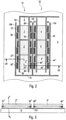
- a top view of a first exemplary embodiment of a lighting element according to the invention is outlined.
- the lighting element has a first OLED module 2 and a second OLED module 4 .
- the first OLED module 2 has in particular a first electrode as an anode, a second electrode as a cathode, and an organic layer arranged between the two electrodes for generating light.
- the first OLED module 2 can be designed in such a way that it only has the two electrodes mentioned as electrodes, ie no further electrodes.
- the first OLED module 2 can also be designed in such a way that the three layers mentioned each extend to the lateral edge regions of the OLED module 2 .
- the first OLED module 2 can be bendable or flexible.
- the second OLED module 4 can be constructed in a corresponding manner.
- the light-emitting element has a carrier element 6 on which the first OLED module 2 and the second OLED module 4 are arranged.
- the carrier element 6 can be an essentially two-dimensional component, for example a plate-shaped component, so that two opposite, large flat sides are formed, with the two OLED modules 2, 4 preferably being arranged on only one of the two flat sides .
- the carrier element 6 can be bendable or flexible.
- the two OLED modules 2, 4 can each be mechanically fixed on the carrier element 6, preferably directly mechanically fixed, for example via a screw connection and/or an adhesive bond.
- the lighting element has electrical conductors 8, 10, which serve to supply electrical power to the two OLED modules 2, 4, specifically comprising a first conductor 10 and a second conductor 8.
- the first OLED module 2 has three contact areas 22, 24, 26 for supplying electric current, namely a first contact area 22, a second contact area 24 and a third contact area 26.
- the three contact areas 22, 24, 26 can - as in 1 indicated - each be elongate and in each case extend along a rectilinear edge region of the first OLED module 2 .
- Each of the three contact areas 22 , 24 , 26 can be electrically conductively connected either to the anode or to the cathode of the first OLED module 2 .
- the second OLED module 4 has three further contact areas 42, 44, 46 for supplying electric power, which are preferably designed in a manner analogous to the three contact areas 22, 24, 26 mentioned first.
- Each of the contact areas 22, 24, 26, 42, 44, 46 is electrically conductively connected to one of the two electrical conductors 8, 10.
- the first contact area 22 is connected to the second conductor 8
- the second contact area 24 is also connected to the second conductor 8
- the third contact area 26 is connected to the first conductor 10.
- the first contact area 22 and the second contact area 24 be electrically conductively connected to the anode of the first OLED module 2 and the third contact region 26 to the cathode of the first OLED module 2. This is particularly advantageous if the anode has a comparatively high resistance, as is the case, for example, when the anode is formed of an ITO layer.
- the further contact areas 42 and 44 of the second OLED module 4 are connected to the second conductor 8 and the further contact area 46 is connected to the first conductor 10.
- two of the three contact areas 22, 24, 26 of the first OLED module 2 can also be connected to the cathode of the first OLED module 2 and the corresponding third contact area to the anode. The same applies to the second OLED module 4.
- connection between the first contact area 22 and the second conductor 8 can be provided, for example, via a conductive adhesive, soft soldering, a flexible cable, a clamp contact or a mechanical spring contact.
- a conductive adhesive for example, via a conductive adhesive, soft soldering, a flexible cable, a clamp contact or a mechanical spring contact.
- the same also applies to the respective connections between the second contact area 24, the third contact area 26 or the other three contact areas 42, 44, 46 and the respective electrical conductor 8, 10.
- the electrical conductors 8 , 10 are at least partially arranged or attached to the carrier element 6 .
- the conductors 8, 10 are arranged on the carrier element 6 in such a way that they do not cross over. This makes it particularly easy to manufacture the Light element allows. This also makes it possible for the appearance of the lighting element to have no crossing points of electrical conductors and is therefore particularly even. This is particularly advantageous if the lighting element is used as the light source of a lamp, for example for room lighting.
- the electrical conductors 8, 10 can be formed from a metal such as aluminum, silver, chromium or copper. They can also be formed from a metal alloy. They can also be made of a transparent material, for example ITO or FTO or ZnO or PEDOT. The material in question can be applied to the carrier element 6, preferably directly to a surface of the carrier element 6. In particular, the conductors 8, 10 can be arranged on only one of the two flat sides of the carrier element 6, in particular on the same flat side as the two OLED modules 2, 4.
- the arrangement of the electrical conductors 8, 10 directly on the carrier element 6 can be designed in such a way that the distances between the contact areas 22, 24, 26 etc. on the one hand and the conductors 8, 10 or arms of the conductors 8, 10 directly on the carrier element 6 on the other hand be less than 5 mm, preferably less than 2 mm.
- the first OLED module 2 can be shaped in such a way that it has a first edge area 50 and a second edge area 52 which is opposite the first edge area 50 .
- the first contact area 22 can be arranged on the first edge area 50 and the second contact area 52 on the second edge area 52, with both the first contact area 22 and the second contact area 24 being connected to one and the same electrode, in particular to the anode, of the first OLED module 2 is connected.
- current can be fed into the first OLED module 2 from two opposite sides, as a result of which a particularly uniform current density distribution is made possible and, as a result, a particularly homogeneous light output.
- the anode of the first OLED module 2 can be in the form of an ITO layer, for example.
- the first OLED module 2 has a rectangular shape, for example a square shape
- a comparatively simple and correspondingly effective contact can be achieved if the first edge region 50 is given by a first side region of the four side regions defined by the rectangular shape and the second edge area 52 through that further side area which is opposite the first side area.
- the first edge area can be provided by a first corner area defined by the rectangular shape and the second edge area by a further corner area that is diagonally opposite the first corner area.
- the lighting element can also have several other OLED modules 2', 2", 4', 4", which are also arranged on the carrier element 6 and are preferably analogous to or structurally identical to the first OLED module 2 or to the second OLED module 4 designed and arranged analogously on the carrier element 6.
- the first OLED module 2, the second OLED module 4 and the further OLED modules 2', 2", 4', 4" are advantageously arranged on the carrier element 6 in such a way that they have rows R1 , R2, R3 and columns form S1, S2 . In this way, it is possible to achieve a light-emitting surface of the lighting element that appears particularly large overall.
- the OLED modules 2, 2′, 2′′, 4, 4′, 4′′ can thus be arranged on the carrier element 6 in a matrix, so to speak.
- the lighting element has a total of six OLED modules 2, 2', 2", 4, 4', 4", with the first OLED module 2 and the second OLED module 4 forming the first row R1 , the further OLED modules labeled 2' and 4' form the second row R2 and the further OLED modules labeled 2" and 4" form the third row R3 .
- the OLED modules 2, 2', 2" form the first column S1 and the OLED modules 4, 4', 4" form the second column S2 .
- any number of rows or columns can obviously be formed in this way by a correspondingly selected number and arrangement of OLED modules, so that the lighting element can in principle be designed with an arbitrarily large light emission area.
- each of the OLED modules 2, 2′, 2′′, 4, 4′, 4′′ can have a light emission area with an area that is greater than 1 cm 2 , preferably greater than 4 cm 2 , particularly preferably greater than 20 cm 2 .
- OLED modules can be used whose light emission areas each have an area of more than 25 cm 2 .
- all OLED modules 2, 2', 2", 4, 4', 4" of the lighting element can have light emission areas with one and the same area size.
- the distances between the OLED modules 2, 2', 2", 4, 4', 4" can be relatively small compared to the size of the light emission areas, so that all OLED modules 2, 2', 2", 4, 4′, 4′′ together give the overall impression of only one, correspondingly large, associated light emission surface of the lighting element.
- the distances between the OLED modules 2, 2', 2", 4, 4', 4" are less than 1 cm, for example between 1 mm and 1 cm. Provision can also be made for the distances in the case of rectangular OLED modules to be less than 30%, preferably less than 15% or less than 10% of one of the edge or side lengths of one of the OLED modules 2, 2', 2''. , 4, 4', 4".
- a simple non-intersecting arrangement of the conductors 8, 10 on the carrier element 6 is in this case made possible if an arm 102 of one of the electrical conductors, in the example shown the first electrical conductor 10, is arranged on the carrier element 6 in a boundary region between two of the columns S1, S2 .
- the arm 102 can be arranged on the carrier element 6 in particular in such a way that it is suitable for the electrical connection to all OLED modules 2, 2′, 2′′ of the relevant column S1 1
- the OLED modules 2, 2' and 2" form the first column S1.
- Each of these OLED modules 2, 2' and 2" is connected to the arm 102, specifically the OLED module 2 via the third contact area 26 , the OLED module 2' via a further contact area 26' and the OLED module 2" via a further contact area 26".
- an arm 82 of a further electrical conductor 8 of the electrical conductors 8, 10 - here the second electrical conductor 8 - can also be arranged on the carrier element 6 in such a way that it is located between those OLED modules 2, 2 ', 2", which form one of the two columns S1, S2 , here forming the first column S1 , on the one hand and the carrier element 6 on the other hand.
- This enables, in particular, a comparatively simple parallel connection of the OLED modules 2, 2', 2" of the relevant column S1 allows.
- the arm 82 is connected to the first OLED module 2 via the first contact region 22, to the further OLED module 2' via a further contact region 22', and to the further OLED module 2' via a further contact region 22''.
- In 2 is a variant of the in 1 outlined light element shown.
- the reference symbols are used analogously.
- the first OLED module 2 has four contact areas 22, 24, 26, 28, with two opposing contact areas being formed in each case, which are connected to one of the two electrodes. Accordingly, in the example shown, the contact areas 22 and 24 arranged opposite one another are electrically connected to the second conductor 8 and the contact areas 26 and 28 also arranged opposite one another to the first conductor 10. A further improvement in the homogeneity of the light emission can be achieved by such a design .
- a further arm 106 of one electrical conductor i.e.
- the first conductor 10 is advantageously provided or arranged on the carrier element 6 for contacting, which, with regard to the column concerned, i.e. here with regard to the column S1, is arranged opposite to the first-mentioned arm 102 of the one or the first electrical conductor 10.
- another arm 84 of the other or the second conductor 8 can also be provided on the carrier element 6 to implement the described opposite current feed , which is opposite of the first-mentioned arm 82 of the other or the second Head 8 is arranged.
- In 3 is a cross section along the mark III-III in 2 sketched.
- This cross section runs through the further OLED module 2", namely through the contact area 22" there and the contact area 26" arranged “height-offset” to this in the sketched plan view and further through the further OLED module 4" and the mutually opposite contact areas 48" and 46".
- the arm 102 which is arranged in the border area between the two columns S1, S2 , is electrically connected on the one hand to the further contact area 26" of the OLED module 2" of one of the two columns S1, S2 and on the other hand to the further contact area 48" of the OLED module 4" is connected to the other of the two columns S1, S2.
- the arm 102 can therefore advantageously be used to supply power to the two columns S1, S2 mentioned.
- a light emission of the light-emitting element can be provided in a first direction o , with reference to FIG 3 upwards, which points away from the carrier element 6 with respect to the first OLED module 2 .
- light emission can also be provided in a second direction u , with reference to FIG 3 downward, which is directed opposite to the first direction o , that is to say with respect to the first OLED module 2 towards the carrier element 6 .
- the carrier element 6 can be made of glass or PMMA or be made of or consist of a film, for example made of PET. If, however, light is only emitted in the first direction o , the carrier element 6 can also be designed to be opaque and consist of metal or plastic, for example.
- the arm 82 of the second conductor 8 can be designed in such a way that it only extends along edge regions 50, 50', 50'' of the relevant OLED modules 2, 2', 2''. In this way it can be achieved that a light emission of the relevant OLED modules 2, 2', 2" is particularly little affected by the arm 82.
- the relevant edge regions 50, 50', 50" only have a width x1 that is less than 25%, preferably less than 20% or less than 10% of an edge length B of the OLED modules 2, 2', 2", for example the width of the relevant column S1 .
- the edge regions relating to the last-mentioned arm 84 in this sense can accordingly have a width x2 which is less than 25%, preferably less than 20% or less than 10% of the edge length B.
- one of the conductors 8, 10, in this case the second conductor 8 has a conductor region 80 which is arranged between the first OLED module 2 and the carrier element 6 and is designed at least partially transparent.
- the conductor area 80 can be formed from a transparent material, for example from ITO or FTO or ZnO or PEDOT.
- the other areas of the second conductor 8 or other conductors 10 can also be designed and arranged accordingly.
- Figure 4a is a corresponding cross-section along the in 4 line labeled IVa in the area of the first OLED module 2.
- the outlined cross section runs through the first contact area 22, the second contact area 24 and the carrier element 6.
- the configuration is such that, viewed in this cross section, an elongated intermediate space 90 is formed between the first OLED module 2 and the carrier element 6 and the conductor area 80 occupies more than half, preferably more than 80%, of the longitudinal extension of the intermediate space 90.
- the conductor area 80 as in Figure 4a the case, the entire length of the gap 90 a.
- the conductor area 80 can be designed with such a large area that it does not form any borders or edges that could significantly interfere with the emission of light in the second direction u or "down".
- the conductor region 80 extends normal to a connecting line between the first contact region 22 and the second contact region 24 - i.e., for example, along the main extent of the first column S1 - likewise advantageously over a larger region of the first OLED module 2, for example again at least 80%, particularly preferably over the entire extent of the first OLED module 2 in this direction.
- the arrangement of the electrical conductors 8, 10 is such that the first conductor 10 extends from a first side, from below in the figures, to the OLED modules 2, 2', 2", 4, 4', 4" and the second conductor 8 from a second side, in the figures from above, which is opposite to the first side with respect to the OLED modules 2, 2', 2", 4, 4', 4".
- Said branches 102, 104 and possibly 106 of the first conductor 10 extend from the first side at least substantially between the columns S1, S2 or along the edges outside the outer columns to the second side.
- the arms 82, 84 of the second conductor 8 or the conductor areas 80, 80', 80'' extend between the relevant OLED modules of the columns S1, S2 on the one hand and the carrier element 6 on the other hand up to the first side.
- this arrangement means that it can be assumed that any differences in the electrical resistances of the conductors 8, 10 can essentially balance out, so that each of the OLED modules 2, 2', 2" of the first column S1 is supplied with the same amount of current can that no differences in brightness between the light emissions of the individual OLED modules 2, 2 ', 2' can be perceived.
- the electrical resistance in this area can be increased in a targeted manner, depending on the length of the incision.
- the power supply to the relevant OLED modules 2, 2', 2" can be influenced in such a way that, in turn, a homogeneously appearing light emission of all OLED modules 2, 2', 2" of the relevant first S column S1 can be achieved.
- a series connection of the OLED modules 2, 2′, 2′′ of the first column S1 or the second column S2 or, if applicable, further columns is provided here.
- the arm 102 of the first electrical conductor 10 is no longer required and thus a distance a between the first column S1 and the second column S2 or more generally between two adjacent columns can be further reduced. This is advantageous with regard to an emission of the luminous element that appears as homogeneous as possible.
- the individual columns S1, S2 can be connected in parallel with each other.
- a plurality of conductor regions 81, 81', 81", 81"' can be provided, in the example shown four, which are located between the OLED modules 2, 2', 2" of the first column S1 on the one hand and the carrier element 6 on the other hand.
- the arrangement is such that in a middle area of the first column S1 each of the conductor areas 81', 81" is arranged overlapping between two adjacent OLED modules and is connected on the one hand to the anode of one of the two OLED modules is electrically connected and on the other hand to the cathode of the other of the two OLED modules.
- the conductor region 81' is electrically connected to the anode of the OLED module 2' on the one hand and to the cathode of the first OLED module 2 on the other hand.
- the conductor area 81 " is electrically connected on the one hand to the anode of the OLED module 2" and on the other hand to the cathode of the OLED module 2'.
- the two edge conductor regions 81, 81''' are each electrically connected to only one OLED module, ie to the first OLED module 2 or the last OLED module 2'' of the relevant column S1 .
- the conductor area 81 is electrically connected to the anode of the first OLED module 2 and the conductor area 81"' to the cathode of the OLED module 2".
- OLED modules are basically flat lighting elements that have a moderate luminance compared to conventional LEDs (LED: light-emitting diode), they are suitable for the production of flat, diffuse light sources.
- LED light-emitting diode
- diffuse lighting is a new way of realizing large-area, high-quality luminaires.
- OLEDs thanks to their thin-film technology, can also be used to create flexible or bendable lighting elements that allow completely new applications in room lighting.
- the present invention shows an efficient design of a corresponding light-emitting element that is comparatively simple to produce.
- the light-emitting element described here can be used directly as a light.
- the lighting element represents the only light source of the lamp.
- several lighting elements can also be used as one lamp.
- several lighting elements can also be provided as a corresponding light source.
Claims (12)
- Elément d'éclairage, présentant- un premier module à OLED (2),- un deuxième module à OLED (4),- un élément de support (6), sur lequel sont disposés le premier module à OLED (2) et le deuxième module à OLED (4), et- des conducteurs (8, 10) électriques servant à alimenter en courant électrique le premier module à OLED (2) et le deuxième module à OLED (4),sachant que le premier module à OLED (2) présente au moins trois zones électriques de contact (22, 24, 26) servant à l'alimentation en courant électrique,le deuxième module à OLED (4) présentant au moins trois autres zones de contact (42, 44, 46) électriques servant à l'alimentation en courant électrique,sachant que chaque zone de contact (22, 24, 26, 42, 44, 46) est reliée de manière électroconductrice respectivement à l'un des conducteurs (8, 10),sachant que les conducteurs (8, 10) électriques sont disposés au moins en partie sur l'élément de support (6), etsachant que les conducteurs (8, 10) sont disposés sur l'élément de support (6) de telle manière qu'ils ne se croisent pas,l'élément d'éclairage présentant en outre,- plusieurs autres modules à OLED (2', 2", 4', 4"), qui sont disposés de la même manière sur l'élément de support (6),sachant que le premier module à OLED (2), le deuxième module à OLED (4) et les autres modules à OLED (2', 2", 4', 4") sont disposés sur l'élément de support (6) de telle manière qu'ils forment des rangées (R1, R2, R3) et des colonnes (S1, S2),caractérisé en cequ'un bras (102) d'un premier conducteur (10) électrique des conducteurs électriques (8, 10) est disposé sur l'élément de support (6) dans une zone limite entre deux des colonnes (S1, S2), sachant que précisément les modules à OLED (2, 2', 2", 4, 4', 4") formant une des deux colonnes (S1, S2) sont branchés d'un point de vue électrique en parallèle et sont reliés électriquement au bras (102) du premier conducteur (10) électrique.
- Elément d'éclairage selon la revendication 1,dans le cadre duquel le premier module à OLED (2) est formé de telle manière qu'il présente une première zone de bord (50) et une deuxième zone de bord (52) en regard de la première zone de bord (50),sachant qu'une première zone de contact (22) des trois zones de contact (22, 24, 26) est reliée électriquement à une première électrode du premier module à OLED (2),sachant qu'une deuxième zone de contact (24) des trois zones de contact (22, 24, 26) est reliée électriquement de la même manière à la première électrode du premier module à OLED (2), etsachant que la première zone de contact (22) est disposée au niveau de la première zone de bord (50) et que la deuxième zone de contact (24) est disposée au niveau de la deuxième zone de bord (52).
- Elément d'éclairage selon la revendication 2,dans le cadre duquel le premier module à OLED (2) présente une forme rectangulaire, en particulier une forme carrée,sachant que la première zone de bord (50) est donnée par une première zone latérale des quatre zones latérales fixées par la forme et que la deuxième zone de bord (52) est donnée par l'autre zone latérale en regard de la première zone latérale, ousachant que la première zone de bord (50) est donnée par une première zone d'angle fixée par la forme et que la deuxième zone de bord (52) est donnée par une autre zone d'angle en regard de la première zone d'angle.
- Elément d'éclairage selon l'une quelconque des revendications précédentes,
sachant qu'en outre un bras (82) d'un deuxième conducteur (8) électrique des conducteurs (8, 10) électriques est disposé sur l'élément de support (6) de telle manière qu'il s'étend entre d'une part précisément les modules à OLED (2, 2', 2") formant l'une des deux colonnes (S1) et d'autre part l'élément de support (6). - Elément d'éclairage selon l'une quelconque des revendications prédédentes,
dans le cadre duquel le premier module à OLED (2), le deuxième module à OLED (4) et les autres modules à OLED (2', 2", 4', 4") présentent respectivement une surface d'émission de lumière, qui est supérieure à 1 cm2, de préférence supérieur à 4 cm2, en particulier de manière préférée supérieure à 20 cm2. - Elément d'éclairage selon l'une quelconque des revendications précédentes,
dans le cadre duquel un conducteur (8) électrique des conducteurs (8, 10) électriques présente une zone conductrice (80, 81) au moins en partie translucide, laquelle est disposée entre le premier module à OLED (2) et l'élément de support (6). - Elément d'éclairage présentant les caractéristiques mentionnées dans les revendications 2 et 6, lequel est configuré de telle manière qu'un espace intermédiaire (90) allongé est formé, dans une section transversale par la première zone de contact (22) et la deuxième zone de contact (24) et l'élément de support (6), entre le premier module à OLED (2) et l'élément de support (6) et la zone conductrice (80, 81) occupe plus de la moitié, de préférence plus de 80 %, en particulier de manière préférée 100 % de l'extension longitudinale de l'espace intermédiaire (90).
- Elément d'éclairage selon l'une quelconque des revendications précédentes,
dans le cadre duquel l'élément de support (6) est au moins en partie translucide et est constitué par exemple de verre, de PMMA ou d'un film, par exemple en PET ou ledit élément de support n'est pas translucide et est constitué par exemple de métal ou de plastique. - Elément d'éclairage selon l'une quelconque des revendications précédentes,
dans le cadre duquel les trois zones de contact (22, 24, 26) électriques sont reliées de manière électroconductrice respectivement à l'un des conducteurs (8, 10) par l'intermédiaire d'une colle conductrice, d'un brasage, d'un câble flexible, d'un contact par serrage ou d'un contact mécanique par ressort. - Elément d'éclairage selon l'une quelconque des revendications précédentes,
dans le cadre duquel les conducteurs (8, 10) électriques sont formés à partir d'un métal, tel que par exemple l'aluminium, l'argent, le chrome ou le cuivre, ou à partir d'un alliage de métal, lequel métal ou alliage de métal est appliqué sur l'élément de support (6), ou lesdits conducteurs sont formés à partir d'un matériau transparent, par exemple à partir d'ITO, de FTO, de ZnO ou de PEDOT, qui est appliqué sur l'élément de support (6). - Lampe, en particulier servant à l'éclairage de pièce,
présentant un élément d'éclairage selon l'une quelconque des revendications précédentes. - Lampe selon la revendication 11,
dans le cadre de laquelle l'élément d'éclairage constitue l'unique source de lumière de la lampe.
Applications Claiming Priority (2)
| Application Number | Priority Date | Filing Date | Title |
|---|---|---|---|
| DE102010042132A DE102010042132A1 (de) | 2010-10-07 | 2010-10-07 | Leuchtelement mit OLED-Modulen |
| PCT/EP2011/067543 WO2012045857A1 (fr) | 2010-10-07 | 2011-10-07 | Élément d'éclairage comprenant des modules delo |
Publications (3)
| Publication Number | Publication Date |
|---|---|
| EP2625731A1 EP2625731A1 (fr) | 2013-08-14 |
| EP2625731B1 EP2625731B1 (fr) | 2014-07-16 |
| EP2625731B2 true EP2625731B2 (fr) | 2022-03-16 |
Family
ID=44759708
Family Applications (1)
| Application Number | Title | Priority Date | Filing Date |
|---|---|---|---|
| EP11764774.3A Active EP2625731B2 (fr) | 2010-10-07 | 2011-10-07 | Élément d'éclairage comprenant des modules delo |
Country Status (3)
| Country | Link |
|---|---|
| EP (1) | EP2625731B2 (fr) |
| DE (1) | DE102010042132A1 (fr) |
| WO (1) | WO2012045857A1 (fr) |
Families Citing this family (11)
| Publication number | Priority date | Publication date | Assignee | Title |
|---|---|---|---|---|
| US8552440B2 (en) * | 2010-12-24 | 2013-10-08 | Semiconductor Energy Laboratory Co., Ltd. | Lighting device |
| JP6231104B2 (ja) | 2012-08-23 | 2017-11-15 | フィリップス ライティング ホールディング ビー ヴィ | 波長変換装置 |
| DE102012221095B4 (de) * | 2012-11-19 | 2020-04-16 | Osram Oled Gmbh | Optoelektronisches Bauelement |
| DE102012223162B4 (de) | 2012-12-14 | 2022-08-25 | Pictiva Displays International Limited | Flächenlichtsystem |
| DE102013109822A1 (de) * | 2013-09-09 | 2015-03-12 | Osram Opto Semiconductors Gmbh | Strahlungsemittierende Vorrichtung und Verfahren zur Herstellung derselben |
| DE102013113001B4 (de) * | 2013-09-13 | 2018-05-24 | Osram Oled Gmbh | Modul und Anordnung mit einem Modul |
| DE102014103751A1 (de) * | 2014-03-19 | 2015-09-24 | Osram Opto Semiconductors Gmbh | Organisches strahlungsemittierendes Bauelement |
| DE102014205747A1 (de) * | 2014-03-27 | 2015-10-01 | Tridonic Gmbh & Co Kg | Leuchtmodul und Herstellungsverfahren für ein Leuchtmodul |
| DE102014112879A1 (de) * | 2014-09-08 | 2016-03-10 | Osram Oled Gmbh | Strahlungsemittierende Vorrichtung und Verfahren zur Herstellung derselben |
| DE102015100099B4 (de) | 2015-01-07 | 2017-10-19 | Osram Oled Gmbh | Verfahren zum Herstellen eines organischen lichtemittierenden Bauelements |
| WO2018139426A1 (fr) * | 2017-01-30 | 2018-08-02 | パイオニア株式会社 | Dispositif électroluminescent |
Citations (6)
| Publication number | Priority date | Publication date | Assignee | Title |
|---|---|---|---|---|
| US20050248935A1 (en) † | 2004-05-04 | 2005-11-10 | Eastman Kodak Company | Tiled flat panel lighting system |
| US20070120167A1 (en) † | 2002-09-30 | 2007-05-31 | Nanosys, Inc. | Large-area nanoenabled macroelectronic substrates and uses therefor |
| WO2008090493A1 (fr) † | 2007-01-22 | 2008-07-31 | Philips Intellectual Property & Standards Gmbh | Dispositif émettant de la lumière |
| US20080264759A1 (en) † | 2007-04-27 | 2008-10-30 | Mechatronic System Company S.R.L. | Switcher for product supply lines |
| US20090114928A1 (en) † | 2005-10-21 | 2009-05-07 | Saint- Gobain Glass France | Lighting structure comprising at least one light-emitting diode, method for making same and uses thereof |
| WO2010033299A1 (fr) † | 2008-09-16 | 2010-03-25 | Osram Sylvania Inc. | Module d'éclairage |
Family Cites Families (3)
| Publication number | Priority date | Publication date | Assignee | Title |
|---|---|---|---|---|
| EP2299781A3 (fr) * | 2004-09-13 | 2011-05-04 | Semiconductor Energy Laboratory Co, Ltd. | Appareil avec une couche émettrice de lumière |
| US7990054B2 (en) * | 2005-12-19 | 2011-08-02 | Koninklijke Philips Electronics N.V. | Organic LED device with electrodes having reduced resistance |
| DE102006016373A1 (de) * | 2006-04-05 | 2007-10-11 | Merck Patent Gmbh | Großflächige OLED's mit homogener Lichtemission |
-
2010
- 2010-10-07 DE DE102010042132A patent/DE102010042132A1/de not_active Withdrawn
-
2011
- 2011-10-07 WO PCT/EP2011/067543 patent/WO2012045857A1/fr active Application Filing
- 2011-10-07 EP EP11764774.3A patent/EP2625731B2/fr active Active
Patent Citations (6)
| Publication number | Priority date | Publication date | Assignee | Title |
|---|---|---|---|---|
| US20070120167A1 (en) † | 2002-09-30 | 2007-05-31 | Nanosys, Inc. | Large-area nanoenabled macroelectronic substrates and uses therefor |
| US20050248935A1 (en) † | 2004-05-04 | 2005-11-10 | Eastman Kodak Company | Tiled flat panel lighting system |
| US20090114928A1 (en) † | 2005-10-21 | 2009-05-07 | Saint- Gobain Glass France | Lighting structure comprising at least one light-emitting diode, method for making same and uses thereof |
| WO2008090493A1 (fr) † | 2007-01-22 | 2008-07-31 | Philips Intellectual Property & Standards Gmbh | Dispositif émettant de la lumière |
| US20080264759A1 (en) † | 2007-04-27 | 2008-10-30 | Mechatronic System Company S.R.L. | Switcher for product supply lines |
| WO2010033299A1 (fr) † | 2008-09-16 | 2010-03-25 | Osram Sylvania Inc. | Module d'éclairage |
Also Published As
| Publication number | Publication date |
|---|---|
| EP2625731A1 (fr) | 2013-08-14 |
| WO2012045857A1 (fr) | 2012-04-12 |
| DE102010042132A1 (de) | 2012-04-26 |
| EP2625731B1 (fr) | 2014-07-16 |
Similar Documents
| Publication | Publication Date | Title |
|---|---|---|
| EP2625731B2 (fr) | Élément d'éclairage comprenant des modules delo | |
| EP2147245B1 (fr) | Dispositif d'éclairage, dispositif de rétroéclairage et dispositif d'affichage | |
| DE102006059509B4 (de) | Organisches Leuchtbauelement | |
| DE102011079014A1 (de) | Leuchtmodul mit reduziertem Flächenbedarf | |
| EP2316143B1 (fr) | Diode électroluminescente organique (delo) et procédé de production d'une delo | |
| DE102007004509A1 (de) | Beleuchtungselement und Verfahren zu seiner Herstellung | |
| DE102006046197B4 (de) | Leuchtmittel und Beleuchtungseinrichtung mit solch einem Leuchtmittel | |
| EP2556288B1 (fr) | Module d'éclairage et lampe | |
| WO2010012276A2 (fr) | Dispositif électroluminescent | |
| DE102012206111B4 (de) | Fotoelektrisches halbleiterelement mit unregelmässig verlaufenden leiterbahnen an einer oberfläche | |
| EP2834862B1 (fr) | Dispositif émetteur de lumière comprenant un élément oled | |
| DE112015005367B4 (de) | Lichtemittierendes Bauelement | |
| DE102010014611A1 (de) | Leuchtmodul und Leuchte | |
| DE102013107675A1 (de) | Bauteil und Verfahren zum Betrieb eines Bauteils | |
| DE102013109822A1 (de) | Strahlungsemittierende Vorrichtung und Verfahren zur Herstellung derselben | |
| DE102016105491A1 (de) | Herstellung von halbleiterbauelementen | |
| DE102015103796A1 (de) | Optoelektronisches Bauelement und Verfahren zum Herstellen eines optoelektronischen Bauelements | |
| EP2924759B1 (fr) | Module d'éclairage et procédé de fabrication d'un module d'éclairage | |
| WO2014067919A1 (fr) | Module lumineux doté d'une mise en contact électrique optimisée | |
| DE102010029843A1 (de) | Flächiger Leuchtkörper mit veränderbarer Leuchtdichte | |
| DE102014103751A1 (de) | Organisches strahlungsemittierendes Bauelement | |
| DE102014116740A1 (de) | Leuchte umfassend wenigstens zwei OLED-Leuchtmittel | |
| DE102014112879A1 (de) | Strahlungsemittierende Vorrichtung und Verfahren zur Herstellung derselben | |
| DE102016121192A1 (de) | Beleuchtungseinrichtung | |
| EP2702436A1 (fr) | Dispositif d'éclairage comprenant des oled ou des qled |
Legal Events
| Date | Code | Title | Description |
|---|---|---|---|
| PUAI | Public reference made under article 153(3) epc to a published international application that has entered the european phase |
Free format text: ORIGINAL CODE: 0009012 |
|
| 17P | Request for examination filed |
Effective date: 20130404 |
|
| AK | Designated contracting states |
Kind code of ref document: A1 Designated state(s): AL AT BE BG CH CY CZ DE DK EE ES FI FR GB GR HR HU IE IS IT LI LT LU LV MC MK MT NL NO PL PT RO RS SE SI SK SM TR |
|
| RIN1 | Information on inventor provided before grant (corrected) |
Inventor name: ERITT, MICHAEL Inventor name: AMELUNG, JOERG Inventor name: KIRCHHOF, CHRISTIAN |
|
| DAX | Request for extension of the european patent (deleted) | ||
| GRAP | Despatch of communication of intention to grant a patent |
Free format text: ORIGINAL CODE: EPIDOSNIGR1 |
|
| RAP1 | Party data changed (applicant data changed or rights of an application transferred) |
Owner name: TRIDONIC DRESDEN GMBH & CO. KG |
|
| INTG | Intention to grant announced |
Effective date: 20140227 |
|
| GRAS | Grant fee paid |
Free format text: ORIGINAL CODE: EPIDOSNIGR3 |
|
| GRAA | (expected) grant |
Free format text: ORIGINAL CODE: 0009210 |
|
| STAA | Information on the status of an ep patent application or granted ep patent |
Free format text: STATUS: THE PATENT HAS BEEN GRANTED |
|
| AK | Designated contracting states |
Kind code of ref document: B1 Designated state(s): AL AT BE BG CH CY CZ DE DK EE ES FI FR GB GR HR HU IE IS IT LI LT LU LV MC MK MT NL NO PL PT RO RS SE SI SK SM TR |
|
| REG | Reference to a national code |
Ref country code: GB Ref legal event code: FG4D Free format text: NOT ENGLISH |
|
| REG | Reference to a national code |
Ref country code: CH Ref legal event code: EP |
|
| REG | Reference to a national code |
Ref country code: IE Ref legal event code: FG4D Free format text: LANGUAGE OF EP DOCUMENT: GERMAN |
|
| REG | Reference to a national code |
Ref country code: AT Ref legal event code: REF Ref document number: 678105 Country of ref document: AT Kind code of ref document: T Effective date: 20140815 |
|
| REG | Reference to a national code |
Ref country code: DE Ref legal event code: R096 Ref document number: 502011003793 Country of ref document: DE Effective date: 20140828 |
|
| REG | Reference to a national code |
Ref country code: NL Ref legal event code: VDEP Effective date: 20140716 |
|
| REG | Reference to a national code |
Ref country code: LT Ref legal event code: MG4D |
|
| PG25 | Lapsed in a contracting state [announced via postgrant information from national office to epo] |
Ref country code: ES Free format text: LAPSE BECAUSE OF FAILURE TO SUBMIT A TRANSLATION OF THE DESCRIPTION OR TO PAY THE FEE WITHIN THE PRESCRIBED TIME-LIMIT Effective date: 20140716 Ref country code: LT Free format text: LAPSE BECAUSE OF FAILURE TO SUBMIT A TRANSLATION OF THE DESCRIPTION OR TO PAY THE FEE WITHIN THE PRESCRIBED TIME-LIMIT Effective date: 20140716 Ref country code: FI Free format text: LAPSE BECAUSE OF FAILURE TO SUBMIT A TRANSLATION OF THE DESCRIPTION OR TO PAY THE FEE WITHIN THE PRESCRIBED TIME-LIMIT Effective date: 20140716 Ref country code: BG Free format text: LAPSE BECAUSE OF FAILURE TO SUBMIT A TRANSLATION OF THE DESCRIPTION OR TO PAY THE FEE WITHIN THE PRESCRIBED TIME-LIMIT Effective date: 20141016 Ref country code: GR Free format text: LAPSE BECAUSE OF FAILURE TO SUBMIT A TRANSLATION OF THE DESCRIPTION OR TO PAY THE FEE WITHIN THE PRESCRIBED TIME-LIMIT Effective date: 20141017 Ref country code: PT Free format text: LAPSE BECAUSE OF FAILURE TO SUBMIT A TRANSLATION OF THE DESCRIPTION OR TO PAY THE FEE WITHIN THE PRESCRIBED TIME-LIMIT Effective date: 20141117 Ref country code: NO Free format text: LAPSE BECAUSE OF FAILURE TO SUBMIT A TRANSLATION OF THE DESCRIPTION OR TO PAY THE FEE WITHIN THE PRESCRIBED TIME-LIMIT Effective date: 20141016 Ref country code: SE Free format text: LAPSE BECAUSE OF FAILURE TO SUBMIT A TRANSLATION OF THE DESCRIPTION OR TO PAY THE FEE WITHIN THE PRESCRIBED TIME-LIMIT Effective date: 20140716 |
|
| PG25 | Lapsed in a contracting state [announced via postgrant information from national office to epo] |
Ref country code: RS Free format text: LAPSE BECAUSE OF FAILURE TO SUBMIT A TRANSLATION OF THE DESCRIPTION OR TO PAY THE FEE WITHIN THE PRESCRIBED TIME-LIMIT Effective date: 20140716 Ref country code: NL Free format text: LAPSE BECAUSE OF FAILURE TO SUBMIT A TRANSLATION OF THE DESCRIPTION OR TO PAY THE FEE WITHIN THE PRESCRIBED TIME-LIMIT Effective date: 20140716 Ref country code: CY Free format text: LAPSE BECAUSE OF FAILURE TO SUBMIT A TRANSLATION OF THE DESCRIPTION OR TO PAY THE FEE WITHIN THE PRESCRIBED TIME-LIMIT Effective date: 20140716 Ref country code: LV Free format text: LAPSE BECAUSE OF FAILURE TO SUBMIT A TRANSLATION OF THE DESCRIPTION OR TO PAY THE FEE WITHIN THE PRESCRIBED TIME-LIMIT Effective date: 20140716 Ref country code: PL Free format text: LAPSE BECAUSE OF FAILURE TO SUBMIT A TRANSLATION OF THE DESCRIPTION OR TO PAY THE FEE WITHIN THE PRESCRIBED TIME-LIMIT Effective date: 20140716 Ref country code: IS Free format text: LAPSE BECAUSE OF FAILURE TO SUBMIT A TRANSLATION OF THE DESCRIPTION OR TO PAY THE FEE WITHIN THE PRESCRIBED TIME-LIMIT Effective date: 20141116 |
|
| REG | Reference to a national code |
Ref country code: DE Ref legal event code: R026 Ref document number: 502011003793 Country of ref document: DE |
|
| PLBI | Opposition filed |
Free format text: ORIGINAL CODE: 0009260 |
|
| PG25 | Lapsed in a contracting state [announced via postgrant information from national office to epo] |
Ref country code: RO Free format text: LAPSE BECAUSE OF FAILURE TO SUBMIT A TRANSLATION OF THE DESCRIPTION OR TO PAY THE FEE WITHIN THE PRESCRIBED TIME-LIMIT Effective date: 20140716 Ref country code: DK Free format text: LAPSE BECAUSE OF FAILURE TO SUBMIT A TRANSLATION OF THE DESCRIPTION OR TO PAY THE FEE WITHIN THE PRESCRIBED TIME-LIMIT Effective date: 20140716 Ref country code: CZ Free format text: LAPSE BECAUSE OF FAILURE TO SUBMIT A TRANSLATION OF THE DESCRIPTION OR TO PAY THE FEE WITHIN THE PRESCRIBED TIME-LIMIT Effective date: 20140716 Ref country code: IT Free format text: LAPSE BECAUSE OF FAILURE TO SUBMIT A TRANSLATION OF THE DESCRIPTION OR TO PAY THE FEE WITHIN THE PRESCRIBED TIME-LIMIT Effective date: 20140716 Ref country code: SK Free format text: LAPSE BECAUSE OF FAILURE TO SUBMIT A TRANSLATION OF THE DESCRIPTION OR TO PAY THE FEE WITHIN THE PRESCRIBED TIME-LIMIT Effective date: 20140716 Ref country code: EE Free format text: LAPSE BECAUSE OF FAILURE TO SUBMIT A TRANSLATION OF THE DESCRIPTION OR TO PAY THE FEE WITHIN THE PRESCRIBED TIME-LIMIT Effective date: 20140716 |
|
| PLAX | Notice of opposition and request to file observation + time limit sent |
Free format text: ORIGINAL CODE: EPIDOSNOBS2 |
|
| 26 | Opposition filed |
Opponent name: OSRAM GMBH Effective date: 20150416 |
|
| PG25 | Lapsed in a contracting state [announced via postgrant information from national office to epo] |
Ref country code: LU Free format text: LAPSE BECAUSE OF FAILURE TO SUBMIT A TRANSLATION OF THE DESCRIPTION OR TO PAY THE FEE WITHIN THE PRESCRIBED TIME-LIMIT Effective date: 20141007 Ref country code: MC Free format text: LAPSE BECAUSE OF FAILURE TO SUBMIT A TRANSLATION OF THE DESCRIPTION OR TO PAY THE FEE WITHIN THE PRESCRIBED TIME-LIMIT Effective date: 20140716 |
|
| REG | Reference to a national code |
Ref country code: CH Ref legal event code: PL |
|
| PG25 | Lapsed in a contracting state [announced via postgrant information from national office to epo] |
Ref country code: BE Free format text: LAPSE BECAUSE OF NON-PAYMENT OF DUE FEES Effective date: 20141031 |
|
| REG | Reference to a national code |
Ref country code: IE Ref legal event code: MM4A |
|
| PG25 | Lapsed in a contracting state [announced via postgrant information from national office to epo] |
Ref country code: LI Free format text: LAPSE BECAUSE OF NON-PAYMENT OF DUE FEES Effective date: 20141031 Ref country code: CH Free format text: LAPSE BECAUSE OF NON-PAYMENT OF DUE FEES Effective date: 20141031 |
|
| PLBB | Reply of patent proprietor to notice(s) of opposition received |
Free format text: ORIGINAL CODE: EPIDOSNOBS3 |
|
| PG25 | Lapsed in a contracting state [announced via postgrant information from national office to epo] |
Ref country code: IE Free format text: LAPSE BECAUSE OF NON-PAYMENT OF DUE FEES Effective date: 20141007 |
|
| REG | Reference to a national code |
Ref country code: FR Ref legal event code: PLFP Year of fee payment: 5 |
|
| PG25 | Lapsed in a contracting state [announced via postgrant information from national office to epo] |
Ref country code: SI Free format text: LAPSE BECAUSE OF FAILURE TO SUBMIT A TRANSLATION OF THE DESCRIPTION OR TO PAY THE FEE WITHIN THE PRESCRIBED TIME-LIMIT Effective date: 20140716 |
|
| PG25 | Lapsed in a contracting state [announced via postgrant information from national office to epo] |
Ref country code: SM Free format text: LAPSE BECAUSE OF FAILURE TO SUBMIT A TRANSLATION OF THE DESCRIPTION OR TO PAY THE FEE WITHIN THE PRESCRIBED TIME-LIMIT Effective date: 20140716 |
|
| PG25 | Lapsed in a contracting state [announced via postgrant information from national office to epo] |
Ref country code: HU Free format text: LAPSE BECAUSE OF FAILURE TO SUBMIT A TRANSLATION OF THE DESCRIPTION OR TO PAY THE FEE WITHIN THE PRESCRIBED TIME-LIMIT; INVALID AB INITIO Effective date: 20111007 Ref country code: HR Free format text: LAPSE BECAUSE OF FAILURE TO SUBMIT A TRANSLATION OF THE DESCRIPTION OR TO PAY THE FEE WITHIN THE PRESCRIBED TIME-LIMIT Effective date: 20140716 Ref country code: TR Free format text: LAPSE BECAUSE OF FAILURE TO SUBMIT A TRANSLATION OF THE DESCRIPTION OR TO PAY THE FEE WITHIN THE PRESCRIBED TIME-LIMIT Effective date: 20140716 Ref country code: MT Free format text: LAPSE BECAUSE OF FAILURE TO SUBMIT A TRANSLATION OF THE DESCRIPTION OR TO PAY THE FEE WITHIN THE PRESCRIBED TIME-LIMIT Effective date: 20140716 |
|
| RAP2 | Party data changed (patent owner data changed or rights of a patent transferred) |
Owner name: TRIDONIC GMBH & CO. KG |
|
| REG | Reference to a national code |
Ref country code: FR Ref legal event code: PLFP Year of fee payment: 6 |
|
| APAH | Appeal reference modified |
Free format text: ORIGINAL CODE: EPIDOSCREFNO |
|
| APBM | Appeal reference recorded |
Free format text: ORIGINAL CODE: EPIDOSNREFNO |
|
| APBP | Date of receipt of notice of appeal recorded |
Free format text: ORIGINAL CODE: EPIDOSNNOA2O |
|
| APBM | Appeal reference recorded |
Free format text: ORIGINAL CODE: EPIDOSNREFNO |
|
| APBP | Date of receipt of notice of appeal recorded |
Free format text: ORIGINAL CODE: EPIDOSNNOA2O |
|
| REG | Reference to a national code |
Ref country code: FR Ref legal event code: PLFP Year of fee payment: 7 |
|
| APBQ | Date of receipt of statement of grounds of appeal recorded |
Free format text: ORIGINAL CODE: EPIDOSNNOA3O |
|
| PGFP | Annual fee paid to national office [announced via postgrant information from national office to epo] |
Ref country code: AT Payment date: 20171027 Year of fee payment: 7 |
|
| PG25 | Lapsed in a contracting state [announced via postgrant information from national office to epo] |
Ref country code: MK Free format text: LAPSE BECAUSE OF FAILURE TO SUBMIT A TRANSLATION OF THE DESCRIPTION OR TO PAY THE FEE WITHIN THE PRESCRIBED TIME-LIMIT Effective date: 20140716 |
|
| REG | Reference to a national code |
Ref country code: FR Ref legal event code: PLFP Year of fee payment: 8 |
|
| PG25 | Lapsed in a contracting state [announced via postgrant information from national office to epo] |
Ref country code: AL Free format text: LAPSE BECAUSE OF FAILURE TO SUBMIT A TRANSLATION OF THE DESCRIPTION OR TO PAY THE FEE WITHIN THE PRESCRIBED TIME-LIMIT Effective date: 20140716 |
|
| PGFP | Annual fee paid to national office [announced via postgrant information from national office to epo] |
Ref country code: GB Payment date: 20181031 Year of fee payment: 8 Ref country code: FR Payment date: 20181025 Year of fee payment: 8 |
|
| REG | Reference to a national code |
Ref country code: AT Ref legal event code: MM01 Ref document number: 678105 Country of ref document: AT Kind code of ref document: T Effective date: 20181007 |
|
| REG | Reference to a national code |
Ref country code: DE Ref legal event code: R084 Ref document number: 502011003793 Country of ref document: DE |
|
| PG25 | Lapsed in a contracting state [announced via postgrant information from national office to epo] |
Ref country code: AT Free format text: LAPSE BECAUSE OF NON-PAYMENT OF DUE FEES Effective date: 20181007 |
|
| GBPC | Gb: european patent ceased through non-payment of renewal fee |
Effective date: 20191007 |
|
| PG25 | Lapsed in a contracting state [announced via postgrant information from national office to epo] |
Ref country code: FR Free format text: LAPSE BECAUSE OF NON-PAYMENT OF DUE FEES Effective date: 20191031 Ref country code: GB Free format text: LAPSE BECAUSE OF NON-PAYMENT OF DUE FEES Effective date: 20191007 |
|
| APBU | Appeal procedure closed |
Free format text: ORIGINAL CODE: EPIDOSNNOA9O |
|
| PUAH | Patent maintained in amended form |
Free format text: ORIGINAL CODE: 0009272 |
|
| STAA | Information on the status of an ep patent application or granted ep patent |
Free format text: STATUS: PATENT MAINTAINED AS AMENDED |
|
| 27A | Patent maintained in amended form |
Effective date: 20220316 |
|
| AK | Designated contracting states |
Kind code of ref document: B2 Designated state(s): AL AT BE BG CH CY CZ DE DK EE ES FI FR GB GR HR HU IE IS IT LI LT LU LV MC MK MT NL NO PL PT RO RS SE SI SK SM TR |
|
| REG | Reference to a national code |
Ref country code: DE Ref legal event code: R102 Ref document number: 502011003793 Country of ref document: DE |
|
| REG | Reference to a national code |
Ref country code: DE Ref legal event code: R081 Ref document number: 502011003793 Country of ref document: DE Owner name: TRIDONIC GMBH & CO. KG, AT Free format text: FORMER OWNER: TRIDONIC DRESDEN GMBH & CO. KG, 01099 DRESDEN, DE |
|
| REG | Reference to a national code |
Ref country code: DE Ref legal event code: R079 Ref document number: 502011003793 Country of ref document: DE Free format text: PREVIOUS MAIN CLASS: H01L0051520000 Ipc: H10K0050800000 |
|
| PGFP | Annual fee paid to national office [announced via postgrant information from national office to epo] |
Ref country code: DE Payment date: 20221028 Year of fee payment: 12 |
|
| P01 | Opt-out of the competence of the unified patent court (upc) registered |
Effective date: 20230530 |