EP2618474A1 - Power conditioner - Google Patents
Power conditioner Download PDFInfo
- Publication number
- EP2618474A1 EP2618474A1 EP11824819.4A EP11824819A EP2618474A1 EP 2618474 A1 EP2618474 A1 EP 2618474A1 EP 11824819 A EP11824819 A EP 11824819A EP 2618474 A1 EP2618474 A1 EP 2618474A1
- Authority
- EP
- European Patent Office
- Prior art keywords
- voltage
- series
- switch elements
- chopper circuit
- sinusoidal
- Prior art date
- Legal status (The legal status is an assumption and is not a legal conclusion. Google has not performed a legal analysis and makes no representation as to the accuracy of the status listed.)
- Withdrawn
Links
Images



Classifications
-
- H—ELECTRICITY
- H02—GENERATION; CONVERSION OR DISTRIBUTION OF ELECTRIC POWER
- H02J—ELECTRIC POWER NETWORKS; CIRCUIT ARRANGEMENTS OR SYSTEMS FOR SUPPLYING OR DISTRIBUTING ELECTRIC POWER; SYSTEMS FOR STORING ELECTRIC ENERGY
- H02J3/00—Circuit arrangements for AC mains or AC distribution networks
- H02J3/38—Arrangements for feeding a single network from two or more generators or sources in parallel; Arrangements for feeding already energised networks from additional generators or sources in parallel
- H02J3/40—Synchronisation of generators for connection to a network or to another generator
-
- H—ELECTRICITY
- H02—GENERATION; CONVERSION OR DISTRIBUTION OF ELECTRIC POWER
- H02M—APPARATUS FOR CONVERSION BETWEEN AC AND AC, BETWEEN AC AND DC, OR BETWEEN DC AND DC, AND FOR USE WITH MAINS OR SIMILAR POWER SUPPLY SYSTEMS; CONVERSION OF DC OR AC INPUT POWER INTO SURGE OUTPUT POWER; CONTROL OR REGULATION THEREOF
- H02M7/00—Conversion of AC power input into DC power output; Conversion of DC power input into AC power output
- H02M7/42—Conversion of DC power input into AC power output without possibility of reversal
- H02M7/44—Conversion of DC power input into AC power output without possibility of reversal by static converters
- H02M7/48—Conversion of DC power input into AC power output without possibility of reversal by static converters using discharge tubes with control electrode or semiconductor devices with control electrode
-
- H—ELECTRICITY
- H02—GENERATION; CONVERSION OR DISTRIBUTION OF ELECTRIC POWER
- H02M—APPARATUS FOR CONVERSION BETWEEN AC AND AC, BETWEEN AC AND DC, OR BETWEEN DC AND DC, AND FOR USE WITH MAINS OR SIMILAR POWER SUPPLY SYSTEMS; CONVERSION OF DC OR AC INPUT POWER INTO SURGE OUTPUT POWER; CONTROL OR REGULATION THEREOF
- H02M7/00—Conversion of AC power input into DC power output; Conversion of DC power input into AC power output
- H02M7/42—Conversion of DC power input into AC power output without possibility of reversal
- H02M7/44—Conversion of DC power input into AC power output without possibility of reversal by static converters
- H02M7/48—Conversion of DC power input into AC power output without possibility of reversal by static converters using discharge tubes with control electrode or semiconductor devices with control electrode
- H02M7/53—Conversion of DC power input into AC power output without possibility of reversal by static converters using discharge tubes with control electrode or semiconductor devices with control electrode using devices of a triode or transistor type requiring continuous application of a control signal
- H02M7/537—Conversion of DC power input into AC power output without possibility of reversal by static converters using discharge tubes with control electrode or semiconductor devices with control electrode using devices of a triode or transistor type requiring continuous application of a control signal using semiconductor devices only, e.g. single switched pulse inverters
- H02M7/539—Conversion of DC power input into AC power output without possibility of reversal by static converters using discharge tubes with control electrode or semiconductor devices with control electrode using devices of a triode or transistor type requiring continuous application of a control signal using semiconductor devices only, e.g. single switched pulse inverters with automatic control of output wave form or frequency
- H02M7/5395—Conversion of DC power input into AC power output without possibility of reversal by static converters using discharge tubes with control electrode or semiconductor devices with control electrode using devices of a triode or transistor type requiring continuous application of a control signal using semiconductor devices only, e.g. single switched pulse inverters with automatic control of output wave form or frequency by pulse-width modulation
-
- H—ELECTRICITY
- H02—GENERATION; CONVERSION OR DISTRIBUTION OF ELECTRIC POWER
- H02J—ELECTRIC POWER NETWORKS; CIRCUIT ARRANGEMENTS OR SYSTEMS FOR SUPPLYING OR DISTRIBUTING ELECTRIC POWER; SYSTEMS FOR STORING ELECTRIC ENERGY
- H02J2101/00—Supply or distribution of decentralised, dispersed or local electric power generation
- H02J2101/20—Dispersed power generation using renewable energy sources
- H02J2101/22—Solar energy
- H02J2101/24—Photovoltaics
-
- H—ELECTRICITY
- H02—GENERATION; CONVERSION OR DISTRIBUTION OF ELECTRIC POWER
- H02J—ELECTRIC POWER NETWORKS; CIRCUIT ARRANGEMENTS OR SYSTEMS FOR SUPPLYING OR DISTRIBUTING ELECTRIC POWER; SYSTEMS FOR STORING ELECTRIC ENERGY
- H02J3/00—Circuit arrangements for AC mains or AC distribution networks
- H02J3/38—Arrangements for feeding a single network from two or more generators or sources in parallel; Arrangements for feeding already energised networks from additional generators or sources in parallel
- H02J3/381—Dispersed generators
-
- H—ELECTRICITY
- H02—GENERATION; CONVERSION OR DISTRIBUTION OF ELECTRIC POWER
- H02M—APPARATUS FOR CONVERSION BETWEEN AC AND AC, BETWEEN AC AND DC, OR BETWEEN DC AND DC, AND FOR USE WITH MAINS OR SIMILAR POWER SUPPLY SYSTEMS; CONVERSION OF DC OR AC INPUT POWER INTO SURGE OUTPUT POWER; CONTROL OR REGULATION THEREOF
- H02M1/00—Details of apparatus for conversion
- H02M1/12—Arrangements for reducing harmonics from AC input or output
-
- Y—GENERAL TAGGING OF NEW TECHNOLOGICAL DEVELOPMENTS; GENERAL TAGGING OF CROSS-SECTIONAL TECHNOLOGIES SPANNING OVER SEVERAL SECTIONS OF THE IPC; TECHNICAL SUBJECTS COVERED BY FORMER USPC CROSS-REFERENCE ART COLLECTIONS [XRACs] AND DIGESTS
- Y02—TECHNOLOGIES OR APPLICATIONS FOR MITIGATION OR ADAPTATION AGAINST CLIMATE CHANGE
- Y02E—REDUCTION OF GREENHOUSE GAS [GHG] EMISSIONS, RELATED TO ENERGY GENERATION, TRANSMISSION OR DISTRIBUTION
- Y02E10/00—Energy generation through renewable energy sources
- Y02E10/50—Photovoltaic [PV] energy
- Y02E10/56—Power conversion systems, e.g. maximum power point trackers
Definitions
- the present invention relates to a power conditioner used in a chopper type power conversion apparatus that chops a DC power to convert the DC power into an AC power.
- a power generation system in which a photovoltaic cell, a fuel cell, and the like having less influence on an environment are used, is actively developed from the viewpoint of global environment protection.
- a DC power from DC power sources such as the photovoltaic cell, which generate an electric power is converted into an AC power having a commercial frequency that is linked to a system by a power conditioner.
- the post-conversion AC power is supplied to a domestic load connected to a commercial electric power system.
- an excess power flows back to a system side when the electric power generated by the DC power source is higher than a consumed power of the domestic load.
- the power conditioner used in the power generation system generally includes an inverter that converts the DC power generated by the photovoltaic cell and the like into the AC power and a protection device that is used in system linkage.
- the power conditioner is roughly divided into an insulation type in which a DC unit and an AC unit are electrically insulated by an insulation transformer and a non-insulation type in which the insulation transformer is not used.
- the non-insulation type is frequently used because the non-insulation type is excellent in power conversion efficiency compared with the insulation type (for example, see Patent Document 1).
- Patent Document 1 Japanese Unexamined Patent Publication No. 2002-10496
- Fig. 8 illustrates a configuration example of a photovoltaic power generation system including a non-insulation type power conditioner.
- a power conditioner 36 performs a linkage operation with a commercial power source 2.
- the power conditioner 36 includes a smoothing capacitor 33, a PWM-control inverter 34, a filter 35 including a reactor and a capacitor, and a control circuit (not illustrated).
- the smoothing capacitor 33 smoothes a power generation output from a photovoltaic panel 1.
- the inverter 34 is constructed by switch elements 37 to 40 that include four MOSFETs in which a diode is connected in inversely parallel.
- Switching control is performed to the switch elements 37 to 40 of the inverter 34 at a high frequency of about 18 kHz, whereby the power generation output of the photovoltaic panel 1, which is smoothed by the smoothing capacitor 33, is converted into the AC power synchronized with the commercial electric power system.
- the power conditioner 36 supplies the converted AC power to a load (not illustrated) through the filter 35 or flows the AC power back to the system side.
- the PWM-control inverter 34 included in the power conditioner 36 it is necessary to convert the DC power having a high voltage, for example, about 800 V from the photovoltaic panel 1 into the AC power by performing the switching operation of the switch elements 37 to 40 at the high frequency of about 18 kHz. Therefore, in the power conversion apparatus including the conventional power conditioner 36, a large switching loss is generated in the electric power conversion of the power conditioner 36, which results in a problem of the low power conversion efficiency.
- An object of the present invention is to provide a power conditioner that suppresses the generation of voltage spikes in a part of the waveform of the sinusoidal voltage in the power conditioner of Japanese Patent Application No. 2009-61915 .
- a power conditioner includes a first group and a second group, a capacitor, and control means.
- Each of the first group and the second group includes two series-connected switch elements.
- the capacitor is connected in parallel with each of the first group and the second group.
- the control means alternately turns on and off the switch elements of the first group at a predetermined frequency, and alternately turns on and off the switch elements of the second group at a frequency higher than the predetermined frequency.
- the control means forms a pulse voltage series that changes in a sinusoidal manner in a first series-connected portion of the switch elements of the first group, forms a difference voltage according to a difference between the pulse voltage series and a sinusoidal voltage in a second series-connected portion of the switch elements of the second group, and controls on/off duty cycles of the switch elements of the second group to obtain the sinusoidal voltage that changes onto positive and negative sides.
- the control means calculates an offset between the timing of chopping between positive and negative of the difference voltage between the pulse voltage series and the sinusoidal voltage and timing of switching between the on/off duty cycles of the switch elements of the second group.
- the control means controls the on/off duty cycles of the switch elements of the second group according to the timing offset related to the calculation.
- a power conditioner includes first to third chopper circuits and control means, in a power conditioner that converts a DC power from a DC power source into an AC power that is system-linked to a commercial power source.
- the first chopper circuit includes a first switch circuit that includes series-connected first and second switch elements. The first and second switch elements are alternately turned on and off at a first frequency, chop a DC voltage from a DC power source at the first frequency, and generate a first pulse voltage series having a voltage in which a voltage level becomes a positive side with respect to a first reference potential.
- the second chopper circuit includes a parallel-connected circuit that includes a second capacitor and a second switch circuit.
- the second switch circuit is constructed by connecting third and fourth switch elements in series.
- the third and fourth switch elements are alternately turned on and off at a second frequency.
- the third and fourth switch elements chop an output of the first chopper circuit at a second frequency higher than predetermined times the first frequency while the first pulse voltage series is set to a second reference potential, and generate a second pulse voltage series having a voltage V2, a voltage level of the voltage V2 being lower than that of the first pulse voltage series, the voltage V2 being a negative side with respect to the second reference potential.
- the third and fourth switch elements adds voltages at the first and second pulse voltage series to form a third pulse voltage series that changes alternately in a sinusoidal manner onto the positive and negative sides with respect to the first reference potential.
- the third chopper circuit includes series-connected fifth and sixth switch elements. A series-connected portion of the fifth and sixth switch elements is connected to a series-connected portion of the third and fourth switch element.
- the fifth and sixth switch elements are alternately turned on and off at a third chopping frequency, and perform a charge and discharge output by chopping the third pulse voltage series according to positive and negative of a difference with a sinusoidal voltage.
- the third chopper circuit further includes series-connected seventh and eighth switch elements.
- the third chopper circuit turns on and off the seventh and eighth switch elements at a PWM frequency higher than the third chopping frequency so as to correct the difference between the third pulse voltage series and the sinusoidal voltage, and the third chopper circuit controls on/off duty cycles of the seventh and eighth switch elements to control the charge and discharge output so as to obtain a sinusoidal voltage that changes continuously on the positive and negative sides of the first reference potential.
- the control means calculates an offset between timing of chopping of the third pulse voltage series according to positive and negative of the difference voltage with the sinusoidal voltage and timing of the switching between on/off duty cycles of the seventh and eighth switch element, and controls the on/off duty cycles of the seventh and eighth switch elements according to the timing offset.
- changing alternately in a sinusoidal manner on positive and negative sides means the positive (one)-side pulse voltage and the negative (the other)-side pulse voltage emerge alternately at a constant cycle with respect to the reference potential, and preferably the pulse cycle is matched with the sinusoidal wave cycle.
- the sinusoidal voltage used to obtain the difference with the pulse voltage series is the sinusoidal voltage that becomes an electric power conversion target, namely, a target value (an instruction value) of the sinusoidal voltage.
- the DC power source means power sources, such as the photovoltaic cell, the fuel cell, and wind power generation, which generate the DC power.
- the present invention can include a power conversion apparatus that chops the DC power to convert the DC power into the AC power. That is, although the present invention has the title of the power conditioner, the power conditioner can include the power conversion apparatus.
- the present invention can be applied to the power conditioner in the power generation system, in which the DC power generated by the DC power source is converted into the AC power by the power conditioner and linked to the commercial power source.
- the generation of the voltage spikes in a part of the waveform of the generated sinusoidal voltage can be suppressed.
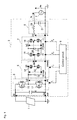
- Fig. 1 is a configuration diagram of a photovoltaic power generation system according to an embodiment of the present invention, and illustrates a configuration in the case of a single-phase two-wire system.
- the photovoltaic power generation system of the embodiment includes a photovoltaic panel 1, and a power conditioner 3 which converts a DC power from the photovoltaic panel 1 into an AC power and performs a linkage operation with a commercial power source 2.
- the photovoltaic panel 1 is configured such that plural photovoltaic modules are connected in series and/or parallel to obtain required electric power.
- the photovoltaic panel 1 of the embodiment is constructed by an amorphous silicon thin-film photovoltaic cell.
- the power conditioner 3 of the embodiment is a non-insulation type transformer-less power conditioner that does not include the insulation transformer.
- the power conditioner 3 includes a first capacitor 4 that is of a smoothing capacitor, first to third chopper circuits 5 to 7, a noise filter 8, and a control circuit 9 that measures voltage at each unit to control the chopper circuits 5 to 7.
- the first to third chopper circuits 5 to 7 and the control circuit 9 constitute a chopper converter that is cascade-connected to the photovoltaic panel 1.
- a negative-electrode side of the photovoltaic panel 1 is connected to the ground.
- a point (a) designates the ground, and the ground has a voltage of zero.
- a point (b) designates a positive-electrode side of the photovoltaic panel 1.
- the first capacitor 4 is connected in parallel between the positive and negative electrodes of the photovoltaic panel 1.
- the first chopper circuit 5 is connected in parallel with the first capacitor 4.
- the first chopper circuit 5 includes first and second switch elements 10 and 11 that are connected in series with each other.
- a diode is connected in inversely parallel with each of the first and second switch elements 10 and 11.
- the first chopper circuit 5 constitutes a first switch circuit using the first and second switch elements 10 and 11.
- first and second switch elements 10 and 11 are constructed by N-channel MOSFETs like switch elements 12 to 17 of the second and third chopper circuits 6 and 7.
- the switch element is not limited to the MOSFET, but an IGBT or a transistor may be used as the switch element.
- the second chopper circuit 6 includes a second capacitor 18 and a second switch circuit that is constructed by series connection of the third and fourth switch elements 12 and 13, in each of which the diode is connected in inversely parallel.
- the second capacitor 18 and the second switch circuit are connected in parallel with each other.
- the ON/OFF control is alternately performed to the third and fourth switch elements 12 and 13 at a second chopping frequency f2, for example, at 100 Hz which is double the first chopping frequency f1.
- a point (c) designates the connection point.
- points (c) and (d) correspond to both capacitor electrode sides of the second capacitor 18.
- the third chopper circuit 7 includes a third switch circuit, a third capacitor 19, and a fourth switch circuit.
- the third switch circuit is constructed by the series connection of the fifth and sixth switch elements 14 and 15, in each of which the diode is connected in inversely parallel.
- the fourth switch circuit is constructed by the series connection of the seventh and eighth switch elements 16 and 17, in each of which the diode is connected in inversely parallel.
- the third switch circuit, the third capacitor 19, and the fourth switch circuit are connected in parallel with one another.
- points (f) and (g) designate one end side and the other end side of the parallel connection of the third switch circuit, the third capacitor 19, and the fourth switch circuit.
- the points (f) and (g) correspond to both capacitor electrode sides of a third capacitor 19.
- the ON/OFF control is alternately performed to the fifth and sixth switch elements 14 and 15 at a third chopping frequency f3, for example, at 150 Hz which is triple the first chopping frequency f1.
- PWM control is performed to the seventh and eighth switch elements 16 and 17 at a high frequency f4, for example, at 18 kHz.
- a point (e) designates the connection point.
- a noise filter 8 including a reactor 20 and a fourth capacitor 21 is connected to the series-connected portion of the seventh and eighth switch elements 16 and 17 in the third chopper circuit 7.
- a point (h) designates the connection point.
- a load (not illustrated) and the commercial power source 2 are connected to the noise filter 8.
- the control circuit 9 measures a system voltage Vs and a system current Is through a differential amplifier circuit (not illustrated), and calculates an instruction value (target sinusoidal voltage) V* of a sinusoidal target voltage synchronized with the system frequency of the commercial power source 2 like the background art.
- the control circuit 9 measures end-to-end voltages Vd1, Vd2, and Vd3 at the first to third capacitors 4, 18, and 19 through the differential amplifier circuit (not illustrated), and generates the gate signal in order to control the chopper circuits 5 to 7.
- the voltage Vd1 is a DC output voltage of the photovoltaic panel 1, which emerges at the point (b) based on the voltage at the point (a) that is of the ground.
- the voltage Vd2 is a charge voltage at the capacitor electrode point (c) of the second capacitor 18 of the second chopper circuit 6 based on the capacitor electrode point (d).
- the voltage Vd3 is a charge voltage at the capacitor electrode point (g) of the third capacitor 19 of the third chopper circuit 7 based on the capacitor electrode point (f).
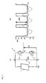
- Fig. 2 is a view schematically illustrating operations of the chopper circuit 5 to 7 of the embodiment.
- Fig. 2(A) is a configuration diagram of a main part in Fig. 1
- Figs. 2(A) to 2(D) illustrate voltages V1, V2, and V3 in Fig. 2(A) .
- Figs. 2(B) and 2(C) a waveform of the target sinusoidal voltage V* synchronized with the system is illustrated by a thin solid line.
- a first reference potential is a potential at the point (a) that is of the ground
- the voltage V1 is the voltage at the point (c) that is of the series-connected portion of the first and second switch elements 10 and 11 in the first chopper circuit 5.
- the voltage V2 is the voltage at the point (e) that is of the series-connected portion of the third and fourth switch elements 12 and 13 in the second chopper circuit 6.
- the voltage V3 is the voltage at the point (h) that is of the series-connected portion of the seventh and eighth switch elements 16 and 17 based on the point (e) that is of the series-connected portion of the fifth and sixth switch elements 14 and 15 in third chopper circuit 7.
- the ON/OFF control is alternately performed to the first and second switch elements 10 and 11 at the first chopping frequency f1 of 50 Hz that is equal to the system frequency.
- a voltage waveform at the point (c) that is of the series-connected portion of the first and second switch elements 10 and 11 becomes a first pulse voltage series including plural pulse voltages of the voltage V1 on the positive side of the potential at the point (a) as illustrated in Fig. 2 (B).
- the voltage V1 becomes the DC output voltage of the photovoltaic panel 1.
- the ON/OFF control is alternately performed to the third and fourth switch elements 12 and 13 at the second chopping frequency f2 of 100 Hz that is double the first chopping frequency f1.
- the voltage V2 at the point (e) that is of the series-connected portion of the third and fourth switch elements 12 and 13 becomes a second pulse voltage series including plural pulse voltages that fall onto the negative side based on the point (c) that is of the series-connected portion of the first and second switch elements 10 and 11.
- a pulse voltage level of the voltage V2 is controlled so as to become 1/2 of the DC output voltage Vd1.
- the voltage V2 at the point (e) that is of the series-connected portion of the third and fourth switch elements 12 and 13 in the second chopper circuit 6 becomes a pulse voltage V1 + V2 in which the voltage V1 between the points (a) and (c) and the voltage V2 between the points (c) and (e) are added as illustrated in Fig. 4(D) .
- the pulse voltage V1 + V2 has a stepwise waveform corresponding to the sinusoidal wave that changes alternately into positive and negative values.
- the stepwise pulse voltage V1 + V2 changes alternately into positive and negative values in synchronization with the target sinusoidal voltage V* illustrated by the thin solid line in Fig. 4(D) .
- the fifth and sixth switch elements 14 and 15 are alternately turned on and off at the third chopping frequency f3 of 150 Hz that is triple the first chopping frequency f1 such that a difference voltage between the stepwise pulse voltage V1 + V2 and the instruction value V* of the target sinusoidal voltage is compensated.
- the seventh and eighth switch elements 16 and 17 are alternately turned on and off at the frequency f4 of 18 kHz.
- the voltage V3 at the point (h) that is of the series-connected portion of the seventh and eighth switch elements 16 and 17 in the third chopper circuit 7 in Fig. 2(A) becomes the positive side when the fifth switch element 14 is off while the sixth switch element 15 is on as illustrated in Fig. 2(D) .
- the voltage V3 becomes the negative side when the fifth switch element 14 is on while the sixth switch element 15 is on.
- Magnitude of the voltage V3 corresponds to the difference voltage between the stepwise-waveform voltage V1 + V2 and the target sinusoidal voltage V*, and the difference voltage corresponds to magnitude of an on/off duty cycle of the seventh and eighth switch elements 17 and 18.
- Fig. 3 is a view illustrating the operating principle of the first chopper circuit 5
- Fig. 3(A) illustrates the photovoltaic panel 1
- the first capacitor 4 and the first chopper circuit 5
- Fig. 3(B) illustrates the voltage V1 between the points (a) and (c).
- the target sinusoidal voltage V* is illustrated by the thin solid line in Fig. 3(B) .
- the DC output voltage Vd1 of the photovoltaic panel 1 emerges at the point (b) that is of the positive-electrode side of the photovoltaic panel 1.
- the DC output voltage Vd1 is smoothed by the first capacitor 4 while the potential at the point (a) that is of the ground is set to the first reference potential.
- the DC output voltage Vd1 is chopped by the first and second switch elements 10 and 11 to which the ON/OFF control is alternately performed at the first frequency f1 of 50 Hz.
- the voltage V1 at the point (c) that is of the series-connected portion of the first and second switch elements 10 and 11 becomes the first pulse voltage series including the plural pulse voltages that rise onto the positive side while the ground potential is set to the first reference potential as illustrated in Fig. 3(B) .
- the pulse voltage V1 is the voltage at the point (c) that is of the series-connected portion of the first and second switch elements 10 and 11 based on the point (a), and the pulse voltage level becomes the DC output voltage Vd1 of the photovoltaic panel 1, for example, 800 V.
- the pulse voltage series in which a phase agrees with that of the system voltage is generated, so that an effective electric power can be output.
- Fig. 4 is a view illustrating the operating principle of the second chopper circuit 6, Fig. 4(A) illustrates the first chopper circuit 5 and the second chopper circuit 6, Fig. 4(B) illustrates the voltage V1, Fig. 4(C) illustrates the voltage V2, and Fig. 4(D) illustrates the voltage V1 + V2.
- the target sinusoidal voltage V* is also illustrated by the thin solid line.
- the voltage V1 at the point (c) in Fig. 4(B) is chopped by the third and fourth switch elements 12 and 13 to which the ON/OFF control is alternately performed at the second chopping frequency f2 of 100 Hz.
- the point (e) that is of the series-connected portion of the third and fourth switch elements 12 and 13 becomes the potential equal to that at the point (c) that is of the series-connected portion of the first and second switch elements 10 and 11 in the first chopper circuit 5.
- the potential at the point (e) that is of the series-connected portion of the third and fourth switch elements 12 and 13 becomes negative compared with the potential at the point (c).
- the voltage V2 at the point (e) that is of the series-connected portion of the third and fourth switch elements 12 and 13 becomes the second pulse voltage series including the plural pulse voltages that fall onto the negative side while the potential at the point (c) that is of the series-connected portion of the first and second switch elements 10 and 11 is set to the second reference potential as illustrated in Fig. 4(C) .
- the second capacitor 18 alternately repeats charge during a charge cycle T1 and discharge during a discharge cycle T2 to generate the pulse voltage that falls onto the negative side based on the second reference potential at the point (c).
- the voltage V2 is the voltage at the point (e) that is of the series-connected portion of the third and fourth switch elements 12 and 13 based on the point (c) that is of the series-connected portion of the first and second switch elements 10 and 11. Accordingly, in the second chopper circuit 6, the voltage V1 + V2 in which the voltage between the points (a) and (c) in Fig. 4 (B) and the voltage between the points (c) and (e) in Fig. 4 (C) are added emerges at the point (e) while the potential at the point (a) that is of the ground is set to the first reference potential. That is, the voltage V1 + V2 becomes the stepwise waveform voltage that changes alternately into positive and negative values according to the change in target sinusoidal voltage V* in Fig.
- Fig. 5 is a view illustrating the operating principle of the third chopper circuit 7.
- Fig. 6 (A) illustrates the stepwise pulse voltage V1 + V2
- Fig. 6 (B) illustrates the voltage V3 at the point (h) that is of the series-connected portion of the seventh and eighth switch elements 16 and 17 based on the point (e) that is of the series-connected portion of the fifth and sixth switch elements 14 and 15.
- the target sinusoidal voltage V* is also illustrated by the thin solid line.
- the ON/OFF control is performed to the fifth and sixth switch elements 14 and 15 in timing corresponding to the positive and negative difference voltage between the stepwise waveform voltage V1 + V2 at the point (e) in Fig. 6 (A) and the target sinusoidal voltage V*.
- the third capacitor 19 is charged and discharged at the voltage V1 + V2 in timing of the ON/OFF control.
- the cycle of the difference voltage is 150 Hz that is of the third chopping frequency f3, and therefore the ON/OFF control is alternately performed to the fifth and sixth switch elements 14 and 15 at the third chopping frequency f3.
- the seventh and eighth switch elements 16 and 17 are controlled at the PWM frequency f4 of 18 kHz that is higher than several hundred times the first chopping frequency f1 on the on/off duty cycle that corrects the difference voltage between the voltage V1 + V2 and the target sinusoidal voltage V*. Therefore, as illustrated in Fig. 6(B) , the voltage V3 corresponding to the difference voltage between the stepwise pulse voltage V1 + V2 and the target sinusoidal voltage V* emerges at the point (h) that is of the series-connected portion of the seventh and eighth switch elements 16 and 17.
- the voltage V3 indicates a PWM average value of the on/off duty cycle control, and the voltage V3 is the voltage at the point (h) that is of the series-connected portion of the seventh and eighth switch elements 16 and 17 based on the point (e) that is of the series-connected portion of the fifth and sixth switch elements 14 and 15.
- the target sinusoidal voltage V* emerges at the point (h) that is of the series-connected portion of the seventh and eighth switch elements 16 and 17 based on the first reference potential at the point (a) that is of the ground.
- the voltage V1 + V2 between the points (a) and (e) in Fig. 6 (A) and the voltage V3 between the points (e) and (h) in Fig. 6(B) are added in the target sinusoidal voltage V*, and the target sinusoidal voltage V* is in-phase with the change in electric power system frequency illustrated by the thin solid line in Fig. 6 (A) .
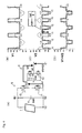
- Fig. 7 (A) illustrates waveforms of the pulse voltage V1 + V2 and the target sinusoidal voltage V*.
- Fig. 7 (B) illustrates switching of the on/off duty cycles of the seventh and eighth switch elements 16 and 17, which corresponds to the difference voltage V3 between the pulse voltage V1 + V2 and the target sinusoidal voltage V* at around a clock time t0.
- Fig. 7 (C) illustrates switching of the on/off duty cycles of the seventh and eighth switch elements 16 and 17, which corresponds to the difference voltage V3 between the pulse voltage V1 + V2 and the target sinusoidal voltage V* at around a clock time t1.
- the on/off duty cycles dx and dy change according to the change in difference voltage V3.
- the on/off duty cycle dx changes gradually before the clock time t0
- the on/off duty cycle dy changes gradually after the clock time t.
- the on/off duty cycle changes suddenly from dx to dy according to the sudden change in difference voltage V3.
- Fig. 7 (B) according to Fig. 7 (A) , the timing in which the difference voltage V3 between the pulse voltage V1 + V2 and the target sinusoidal voltage V* switches from the relationship of V1 + V2 ⁇ V* to the relationship of V1 + V2 > V* at the clock time t0 agrees ideally with the timing in which the on/off duty cycles of the seventh and eighth switch elements 16 and 17, which corresponds to the difference voltage V3, switches from the on/off duty cycle dx to the on/off duty cycle dy.
- Fig. 7 (D) illustrates a waveform of the difference voltage V3 in Fig. 7 (A) .
- the timing in which the difference voltage V3 changes suddenly is deviated from the timing in which the on/off duty cycle switches from the on/off duty cycle dx to the on/off duty cycle dy. Therefore, as illustrated in Fig. 7 (E) , the voltage spike Vs1 is generated in the target sinusoidal voltage V at the actual point (h).
- the offset is a clock time difference ⁇ t between the clock times t0 and t1.
- the control circuit 9 controls the on/off duty cycles of the seventh and eighth switch elements 16 and 17 according to the timing offset ⁇ t using internal duty control means such that the on/off duty cycle is set to the on/off duty cycle dx before the clock time t0 as illustrated in Fig. 7 (F) , and such that the on/off duty cycle is set to the on/off duty cycle dy' during the timing offset ⁇ t after the clock time t0 as illustrated in Fig. 7 (F) .
- the control circuit 9 sets the on/off duty cycle to the on/off duty cycle dy.
- the on/off duty cycle dy' is less than or equal to 100% when the on/off duty cycle dy is 100%, and the on/off duty cycle dy' is greater than or equal to 0% when the on/off duty cycle dy is 0%.
- a voltage spike Vs1 is generated in the target sinusoidal voltage V* during clock time t0 to ⁇ t.
- a voltage spike Vs2 having a polarity opposite to that of the voltage spike Vs1 is caused to emerge after ⁇ t to cancel the voltage spike Vs1.
- the voltage spike waveform is suppressed in the waveform of the sinusoidal voltage V*. Therefore, as illustrated in Fig. 7(H) , a broken-line spike current corresponding to the voltage spike Vs1 is eliminated in a sinusoidal current I.
- the calculation means calculates the offset between the timing in which the third pulse voltage series is chopped according to the positive and negative of the difference with the sinusoidal voltage and the timing of the switching between the on/off duty cycles of the seventh and eighth switch elements.
- the duty control means controls the on/off duty cycles of the seventh and eighth switch elements according to the timing offset. Therefore, the generation of the voltage spike in part of the waveform of the sinusoidal voltage V* is suppressed.
- the calculation means and the duty control means can be implemented by software in the control circuit.
- the present invention includes a power conversion apparatus including a first chopper circuit, a second chopper circuit, and a third chopper circuit.
- the present invention includes a power generation system including the DC power source and the power conditioner connected to the DC power source.
- the power generation system converts the DC power generated by the DC power source into the AC power with the power conditioner, and performs the linkage operation with the commercial power source.
- the power conditioner includes the power generation system including pulse voltage generating means and sinusoidal voltage generating means.
- the present invention includes a power generation system including the DC power source and the power conditioner connected to the DC power source.
- the power generation system converts the DC power generated by the DC power source into the AC power with the power conditioner, and performs the linkage operation with the commercial power source.
- the power conditioner includes a first chopper circuit, a second chopper circuit, and a third chopper circuit.
Landscapes
- Engineering & Computer Science (AREA)
- Power Engineering (AREA)
- Inverter Devices (AREA)
- Dc-Dc Converters (AREA)
- Supply And Distribution Of Alternating Current (AREA)
- Charge And Discharge Circuits For Batteries Or The Like (AREA)
Abstract
Description
- The present invention relates to a power conditioner used in a chopper type power conversion apparatus that chops a DC power to convert the DC power into an AC power.
- Nowadays, a power generation system, in which a photovoltaic cell, a fuel cell, and the like having less influence on an environment are used, is actively developed from the viewpoint of global environment protection.
- In some of the power generation systems, a DC power from DC power sources such as the photovoltaic cell, which generate an electric power, is converted into an AC power having a commercial frequency that is linked to a system by a power conditioner. The post-conversion AC power is supplied to a domestic load connected to a commercial electric power system. On the other hand, an excess power flows back to a system side when the electric power generated by the DC power source is higher than a consumed power of the domestic load.
- The power conditioner used in the power generation system generally includes an inverter that converts the DC power generated by the photovoltaic cell and the like into the AC power and a protection device that is used in system linkage. The power conditioner is roughly divided into an insulation type in which a DC unit and an AC unit are electrically insulated by an insulation transformer and a non-insulation type in which the insulation transformer is not used. The non-insulation type is frequently used because the non-insulation type is excellent in power conversion efficiency compared with the insulation type (for example, see Patent Document 1).
- Patent Document 1: Japanese Unexamined Patent Publication No.
2002-10496 -
Fig. 8 illustrates a configuration example of a photovoltaic power generation system including a non-insulation type power conditioner. Apower conditioner 36 performs a linkage operation with acommercial power source 2. Thepower conditioner 36 includes asmoothing capacitor 33, a PWM-control inverter 34, afilter 35 including a reactor and a capacitor, and a control circuit (not illustrated). Thesmoothing capacitor 33 smoothes a power generation output from a photovoltaic panel 1. Theinverter 34 is constructed byswitch elements 37 to 40 that include four MOSFETs in which a diode is connected in inversely parallel. Switching control is performed to theswitch elements 37 to 40 of theinverter 34 at a high frequency of about 18 kHz, whereby the power generation output of the photovoltaic panel 1, which is smoothed by thesmoothing capacitor 33, is converted into the AC power synchronized with the commercial electric power system. Thepower conditioner 36 supplies the converted AC power to a load (not illustrated) through thefilter 35 or flows the AC power back to the system side. - In the PWM-
control inverter 34 included in thepower conditioner 36, it is necessary to convert the DC power having a high voltage, for example, about 800 V from the photovoltaic panel 1 into the AC power by performing the switching operation of theswitch elements 37 to 40 at the high frequency of about 18 kHz. Therefore, in the power conversion apparatus including theconventional power conditioner 36, a large switching loss is generated in the electric power conversion of thepower conditioner 36, which results in a problem of the low power conversion efficiency. - In order to solve the problem, the inventors filed Japanese Patent Application No.
2009-61915 - However, in the power conditioner of Japanese Patent Application No.
2009-61915 - An object of the present invention is to provide a power conditioner that suppresses the generation of voltage spikes in a part of the waveform of the sinusoidal voltage in the power conditioner of Japanese Patent Application No.
2009-61915 - A power conditioner according to a first aspect of the present invention includes a first group and a second group, a capacitor, and control means. Each of the first group and the second group includes two series-connected switch elements. The capacitor is connected in parallel with each of the first group and the second group. The control means alternately turns on and off the switch elements of the first group at a predetermined frequency, and alternately turns on and off the switch elements of the second group at a frequency higher than the predetermined frequency. The control means forms a pulse voltage series that changes in a sinusoidal manner in a first series-connected portion of the switch elements of the first group, forms a difference voltage according to a difference between the pulse voltage series and a sinusoidal voltage in a second series-connected portion of the switch elements of the second group, and controls on/off duty cycles of the switch elements of the second group to obtain the sinusoidal voltage that changes onto positive and negative sides. The control means calculates an offset between the timing of chopping between positive and negative of the difference voltage between the pulse voltage series and the sinusoidal voltage and timing of switching between the on/off duty cycles of the switch elements of the second group. The control means controls the on/off duty cycles of the switch elements of the second group according to the timing offset related to the calculation.
- A power conditioner according to a second aspect of the present invention includes first to third chopper circuits and control means, in a power conditioner that converts a DC power from a DC power source into an AC power that is system-linked to a commercial power source. The first chopper circuit includes a first switch circuit that includes series-connected first and second switch elements. The first and second switch elements are alternately turned on and off at a first frequency, chop a DC voltage from a DC power source at the first frequency, and generate a first pulse voltage series having a voltage in which a voltage level becomes a positive side with respect to a first reference potential. The second chopper circuit includes a parallel-connected circuit that includes a second capacitor and a second switch circuit. One side of a parallel connection of the parallel-connected circuit is connected to the series-connected portion of the first and second switch elements. The second switch circuit is constructed by connecting third and fourth switch elements in series. The third and fourth switch elements are alternately turned on and off at a second frequency. The third and fourth switch elements chop an output of the first chopper circuit at a second frequency higher than predetermined times the first frequency while the first pulse voltage series is set to a second reference potential, and generate a second pulse voltage series having a voltage V2, a voltage level of the voltage V2 being lower than that of the first pulse voltage series, the voltage V2 being a negative side with respect to the second reference potential. The third and fourth switch elements adds voltages at the first and second pulse voltage series to form a third pulse voltage series that changes alternately in a sinusoidal manner onto the positive and negative sides with respect to the first reference potential. The third chopper circuit includes series-connected fifth and sixth switch elements. A series-connected portion of the fifth and sixth switch elements is connected to a series-connected portion of the third and fourth switch element. The fifth and sixth switch elements are alternately turned on and off at a third chopping frequency, and perform a charge and discharge output by chopping the third pulse voltage series according to positive and negative of a difference with a sinusoidal voltage. The third chopper circuit further includes series-connected seventh and eighth switch elements. The third chopper circuit turns on and off the seventh and eighth switch elements at a PWM frequency higher than the third chopping frequency so as to correct the difference between the third pulse voltage series and the sinusoidal voltage, and the third chopper circuit controls on/off duty cycles of the seventh and eighth switch elements to control the charge and discharge output so as to obtain a sinusoidal voltage that changes continuously on the positive and negative sides of the first reference potential. The control means calculates an offset between timing of chopping of the third pulse voltage series according to positive and negative of the difference voltage with the sinusoidal voltage and timing of the switching between on/off duty cycles of the seventh and eighth switch element, and controls the on/off duty cycles of the seventh and eighth switch elements according to the timing offset.
- As used herein, "changing alternately in a sinusoidal manner on positive and negative sides" means the positive (one)-side pulse voltage and the negative (the other)-side pulse voltage emerge alternately at a constant cycle with respect to the reference potential, and preferably the pulse cycle is matched with the sinusoidal wave cycle.
- Preferably the sinusoidal voltage used to obtain the difference with the pulse voltage series is the sinusoidal voltage that becomes an electric power conversion target, namely, a target value (an instruction value) of the sinusoidal voltage.
- The DC power source means power sources, such as the photovoltaic cell, the fuel cell, and wind power generation, which generate the DC power.
- The present invention can include a power conversion apparatus that chops the DC power to convert the DC power into the AC power. That is, although the present invention has the title of the power conditioner, the power conditioner can include the power conversion apparatus.
- The present invention can be applied to the power conditioner in the power generation system, in which the DC power generated by the DC power source is converted into the AC power by the power conditioner and linked to the commercial power source.
- According to the present invention, the generation of the voltage spikes in a part of the waveform of the generated sinusoidal voltage can be suppressed.
-
-
Fig. 1 is a configuration diagram of a photovoltaic power generation system according to an embodiment of the present invention. -
Fig. 2 is a view illustrating an operation of a power conditioner inFig. 1 . -
Fig. 3 is a view illustrating an operating principle of a first chopper circuit inFig. 1 . -
Fig. 4 is a view illustrating an operating principle of a second chopper circuit inFig. 1 . -
Fig. 5 is a view illustrating an operating principle of a third chopper circuit inFig. 1 . -
Fig. 6 is a view illustrating a voltage waveform of each unit inFig. 5 . -
Fig. 7 is a view illustrating a timing chart in which a voltage spike is eliminated from a sinusoidal voltage waveform. -
Fig. 8 is a configuration diagram of a conventional example. - Hereinafter, an embodiment of the present invention will be described with reference to the drawings.
-
Fig. 1 is a configuration diagram of a photovoltaic power generation system according to an embodiment of the present invention, and illustrates a configuration in the case of a single-phase two-wire system. - The photovoltaic power generation system of the embodiment includes a photovoltaic panel 1, and a
power conditioner 3 which converts a DC power from the photovoltaic panel 1 into an AC power and performs a linkage operation with acommercial power source 2. - The photovoltaic panel 1 is configured such that plural photovoltaic modules are connected in series and/or parallel to obtain required electric power. The photovoltaic panel 1 of the embodiment is constructed by an amorphous silicon thin-film photovoltaic cell. The
power conditioner 3 of the embodiment is a non-insulation type transformer-less power conditioner that does not include the insulation transformer. Thepower conditioner 3 includes afirst capacitor 4 that is of a smoothing capacitor, first tothird chopper circuits 5 to 7, anoise filter 8, and acontrol circuit 9 that measures voltage at each unit to control thechopper circuits 5 to 7. - The first to
third chopper circuits 5 to 7 and thecontrol circuit 9 constitute a chopper converter that is cascade-connected to the photovoltaic panel 1. A negative-electrode side of the photovoltaic panel 1 is connected to the ground. InFig. 1 , a point (a) designates the ground, and the ground has a voltage of zero. A point (b) designates a positive-electrode side of the photovoltaic panel 1. Thefirst capacitor 4 is connected in parallel between the positive and negative electrodes of the photovoltaic panel 1. - The
first chopper circuit 5 is connected in parallel with thefirst capacitor 4. Thefirst chopper circuit 5 includes first andsecond switch elements second switch elements - The
first chopper circuit 5 constitutes a first switch circuit using the first andsecond switch elements - In the
first chopper circuit 5, using a gate signal from thecontrol circuit 9, ON/OFF control is alternately performed to the first andsecond switch elements second switch elements switch elements 12 to 17 of the second andthird chopper circuits - The
second chopper circuit 6 includes asecond capacitor 18 and a second switch circuit that is constructed by series connection of the third andfourth switch elements second capacitor 18 and the second switch circuit are connected in parallel with each other. Using the gate signal from thecontrol circuit 9, the ON/OFF control is alternately performed to the third andfourth switch elements - One end side of the parallel connection of the
second capacitor 18 and the second switch circuit in thesecond chopper circuit 6 is connected to a series-connected portion of the first andsecond switch elements first chopper circuit 5. InFig. 1 , a point (c) designates the connection point. InFig. 1 , points (c) and (d) correspond to both capacitor electrode sides of thesecond capacitor 18. - The
third chopper circuit 7 includes a third switch circuit, athird capacitor 19, and a fourth switch circuit. The third switch circuit is constructed by the series connection of the fifth andsixth switch elements eighth switch elements third chopper circuit 7, the third switch circuit, thethird capacitor 19, and the fourth switch circuit are connected in parallel with one another. InFig. 1 , points (f) and (g) designate one end side and the other end side of the parallel connection of the third switch circuit, thethird capacitor 19, and the fourth switch circuit. The points (f) and (g) correspond to both capacitor electrode sides of athird capacitor 19. - Using the gate signal from the
control circuit 9, the ON/OFF control is alternately performed to the fifth andsixth switch elements - Using the gate signal from the
control circuit 9, PWM control is performed to the seventh andeighth switch elements - The series-connected portion of the fifth and
sixth switch elements third chopper circuit 7 is connected to the series-connected portion of the third andfourth switch elements second chopper circuit 6. InFig. 1 , a point (e) designates the connection point. - A
noise filter 8 including areactor 20 and afourth capacitor 21 is connected to the series-connected portion of the seventh andeighth switch elements third chopper circuit 7. InFig. 1 , a point (h) designates the connection point. - A load (not illustrated) and the
commercial power source 2 are connected to thenoise filter 8. - The
control circuit 9 measures a system voltage Vs and a system current Is through a differential amplifier circuit (not illustrated), and calculates an instruction value (target sinusoidal voltage) V* of a sinusoidal target voltage synchronized with the system frequency of thecommercial power source 2 like the background art. Thecontrol circuit 9 measures end-to-end voltages Vd1, Vd2, and Vd3 at the first tothird capacitors chopper circuits 5 to 7. - The voltage Vd1 is a DC output voltage of the photovoltaic panel 1, which emerges at the point (b) based on the voltage at the point (a) that is of the ground.
- The voltage Vd2 is a charge voltage at the capacitor electrode point (c) of the
second capacitor 18 of thesecond chopper circuit 6 based on the capacitor electrode point (d). - The voltage Vd3 is a charge voltage at the capacitor electrode point (g) of the
third capacitor 19 of thethird chopper circuit 7 based on the capacitor electrode point (f). -
Fig. 2 is a view schematically illustrating operations of thechopper circuit 5 to 7 of the embodiment.Fig. 2(A) is a configuration diagram of a main part inFig. 1 , andFigs. 2(A) to 2(D) illustrate voltages V1, V2, and V3 inFig. 2(A) . InFigs. 2(B) and 2(C) , a waveform of the target sinusoidal voltage V* synchronized with the system is illustrated by a thin solid line. - Assuming that a first reference potential is a potential at the point (a) that is of the ground, the voltage V1 is the voltage at the point (c) that is of the series-connected portion of the first and
second switch elements first chopper circuit 5. - Assuming that a second reference potential is a potential at the point (c), the voltage V2 is the voltage at the point (e) that is of the series-connected portion of the third and
fourth switch elements second chopper circuit 6. - The voltage V3 is the voltage at the point (h) that is of the series-connected portion of the seventh and
eighth switch elements sixth switch elements third chopper circuit 7. - In the case of 50 Hz that is equal to the system frequency of the
commercial power source 2, in thefirst chopper circuit 5, the ON/OFF control is alternately performed to the first andsecond switch elements - Therefore, a voltage waveform at the point (c) that is of the series-connected portion of the first and
second switch elements Fig. 2 (B). The voltage V1 becomes the DC output voltage of the photovoltaic panel 1. - In the
second chopper circuit 6, the ON/OFF control is alternately performed to the third andfourth switch elements - Therefore, as illustrated in
Fig. 2(C) , the voltage V2 at the point (e) that is of the series-connected portion of the third andfourth switch elements second switch elements - A pulse voltage level of the voltage V2 is controlled so as to become 1/2 of the DC output voltage Vd1.
- Based on the point (a) that is of the ground, namely, based on the first reference potential, the voltage V2 at the point (e) that is of the series-connected portion of the third and
fourth switch elements second chopper circuit 6 becomes a pulse voltage V1 + V2 in which the voltage V1 between the points (a) and (c) and the voltage V2 between the points (c) and (e) are added as illustrated inFig. 4(D) . That is, the pulse voltage V1 + V2 has a stepwise waveform corresponding to the sinusoidal wave that changes alternately into positive and negative values. The stepwise pulse voltage V1 + V2 changes alternately into positive and negative values in synchronization with the target sinusoidal voltage V* illustrated by the thin solid line inFig. 4(D) . - In the
third chopper circuit 7, the fifth andsixth switch elements third chopper circuit 7, the seventh andeighth switch elements - Therefore, the voltage V3 at the point (h) that is of the series-connected portion of the seventh and
eighth switch elements third chopper circuit 7 inFig. 2(A) becomes the positive side when thefifth switch element 14 is off while thesixth switch element 15 is on as illustrated inFig. 2(D) . The voltage V3 becomes the negative side when thefifth switch element 14 is on while thesixth switch element 15 is on. Magnitude of the voltage V3 corresponds to the difference voltage between the stepwise-waveform voltage V1 + V2 and the target sinusoidal voltage V*, and the difference voltage corresponds to magnitude of an on/off duty cycle of the seventh andeighth switch elements - Operating principles of the first to
third chopper circuits 5 to 7 will be described in detail below. -
Fig. 3 is a view illustrating the operating principle of thefirst chopper circuit 5,Fig. 3(A) illustrates the photovoltaic panel 1, thefirst capacitor 4, and thefirst chopper circuit 5, andFig. 3(B) illustrates the voltage V1 between the points (a) and (c). Particularly, the target sinusoidal voltage V* is illustrated by the thin solid line inFig. 3(B) . - The DC output voltage Vd1 of the photovoltaic panel 1 emerges at the point (b) that is of the positive-electrode side of the photovoltaic panel 1. The DC output voltage Vd1 is smoothed by the
first capacitor 4 while the potential at the point (a) that is of the ground is set to the first reference potential. - In the
first chopper circuit 5, the DC output voltage Vd1 is chopped by the first andsecond switch elements - When the
first switch element 10 is on while thesecond switch element 11 is off, the charge voltage Vd1 of thefirst capacitor 4 that is of the voltage at the point (b) emerges at the point (c) that is of the series-connected portion of the first andsecond switch elements first chopper circuit 5. - When the
first switch element 10 is off while thesecond switch element 11 is on, the ground voltage at the point (a) emerges at the point (c) that is of the series-connected portion of the first andsecond switch elements first chopper circuit 5. - Accordingly, as described above, the voltage V1 at the point (c) that is of the series-connected portion of the first and
second switch elements Fig. 3(B) . The pulse voltage V1 is the voltage at the point (c) that is of the series-connected portion of the first andsecond switch elements - In the
first chopper circuit 5, the pulse voltage series in which a phase agrees with that of the system voltage is generated, so that an effective electric power can be output. -
Fig. 4 is a view illustrating the operating principle of thesecond chopper circuit 6,Fig. 4(A) illustrates thefirst chopper circuit 5 and thesecond chopper circuit 6,Fig. 4(B) illustrates the voltage V1,Fig. 4(C) illustrates the voltage V2, andFig. 4(D) illustrates the voltage V1 + V2. InFigs. 4(B) to 4(D) , the target sinusoidal voltage V* is also illustrated by the thin solid line. - In the
second chopper circuit 6, the voltage V1 at the point (c) inFig. 4(B) is chopped by the third andfourth switch elements - When the
third switch element 12 is on while thefourth switch element 13 is off, the point (e) that is of the series-connected portion of the third andfourth switch elements second switch elements first chopper circuit 5. When thethird switch element 12 is off while thefourth switch element 13 is on, the potential at the point (e) that is of the series-connected portion of the third andfourth switch elements fourth switch elements second switch elements Fig. 4(C) . - When the
first switch element 10 of thefirst chopper circuit 5 is turned on while thesecond switch element 11 turned off, thethird switch element 12 of thesecond chopper circuit 6 is turned off, and thefourth switch element 13 is turned on, thereby charging thesecond capacitor 18. When thefirst switch element 10 of thefirst chopper circuit 5 is turned off while thesecond switch element 11 turned on, thethird switch element 12 of thesecond chopper circuit 6 is turned off, and thefourth switch element 13 is turned on, whereby thesecond capacitor 18 is discharged through theswitch elements Fig. 4(C) , thesecond capacitor 18 alternately repeats charge during a charge cycle T1 and discharge during a discharge cycle T2 to generate the pulse voltage that falls onto the negative side based on the second reference potential at the point (c). The voltage level Vd2 of the pulse is a half (Vd2 = -Vd1/2) of the DC output voltage Vd1 of the photovoltaic panel 1, for example, 400 V. - The voltage V2 is the voltage at the point (e) that is of the series-connected portion of the third and
fourth switch elements second switch elements second chopper circuit 6, the voltage V1 + V2 in which the voltage between the points (a) and (c) inFig. 4 (B) and the voltage between the points (c) and (e) inFig. 4 (C) are added emerges at the point (e) while the potential at the point (a) that is of the ground is set to the first reference potential. That is, the voltage V1 + V2 becomes the stepwise waveform voltage that changes alternately into positive and negative values according to the change in target sinusoidal voltage V* inFig. 4 (D) . In thesecond chopper circuit 6, the pulse voltage series that falls onto the negative side is generated, so that the even harmonics can be removed. In thesecond chopper circuit 6, the charge and the discharge are repeated with the equal electric power, the effective electric power becomes zero in principle. -
Fig. 5 is a view illustrating the operating principle of thethird chopper circuit 7.Fig. 6 (A) illustrates the stepwise pulse voltage V1 + V2, andFig. 6 (B) illustrates the voltage V3 at the point (h) that is of the series-connected portion of the seventh andeighth switch elements sixth switch elements Fig. 6 (A) , the target sinusoidal voltage V* is also illustrated by the thin solid line. - The ON/OFF control is performed to the fifth and
sixth switch elements Fig. 6 (A) and the target sinusoidal voltage V*. As a result, thethird capacitor 19 is charged and discharged at the voltage V1 + V2 in timing of the ON/OFF control. - In other words, when the voltage V1 + V2 is larger than the target sinusoidal voltage V* (voltage V1 + V2 > target sinusoidal voltage V*), the difference voltage is positive, the
fifth switch element 14 is controlled on, and thesixth switch element 15 is controlled off. Therefore, thethird capacitor 19 is charged at the voltage V1 + V2. - On the other hand, when the voltage V1 + V2 is smaller than the target sinusoidal voltage V* (voltage V1 + V2 < target sinusoidal voltage V*), the difference voltage is negative, the
fifth switch element 14 is controlled off, and thesixth switch element 15 is controlled on. Therefore, thethird capacitor 19 charged at the voltage V1 + V2 is discharged. - The cycle of the difference voltage is 150 Hz that is of the third chopping frequency f3, and therefore the ON/OFF control is alternately performed to the fifth and
sixth switch elements - Additionally, in the
third chopper circuit 7, the seventh andeighth switch elements Fig. 6(B) , the voltage V3 corresponding to the difference voltage between the stepwise pulse voltage V1 + V2 and the target sinusoidal voltage V* emerges at the point (h) that is of the series-connected portion of the seventh andeighth switch elements - The voltage V3 indicates a PWM average value of the on/off duty cycle control, and the voltage V3 is the voltage at the point (h) that is of the series-connected portion of the seventh and
eighth switch elements sixth switch elements - Accordingly, in the
third chopper circuit 7, the target sinusoidal voltage V* emerges at the point (h) that is of the series-connected portion of the seventh andeighth switch elements Fig. 6 (A) and the voltage V3 between the points (e) and (h) inFig. 6(B) are added in the target sinusoidal voltage V*, and the target sinusoidal voltage V* is in-phase with the change in electric power system frequency illustrated by the thin solid line inFig. 6 (A) . - The suppression of generation of a voltage spike in part of the target sinusoidal voltage V* in the power conditioner will be described below with reference to
Fig. 7. Fig. 7 (A) illustrates waveforms of the pulse voltage V1 + V2 and the target sinusoidal voltage V*.Fig. 7 (B) illustrates switching of the on/off duty cycles of the seventh andeighth switch elements Fig. 7 (C) illustrates switching of the on/off duty cycles of the seventh andeighth switch elements Fig. 7 (B) and an on/off duty cycle dy after the clock time t0, the on/off duty cycles dx and dy change according to the change in difference voltage V3. The on/off duty cycle dx changes gradually before the clock time t0, and the on/off duty cycle dy changes gradually after the clock time t. At the clock time t0, the on/off duty cycle changes suddenly from dx to dy according to the sudden change in difference voltage V3. - In
Fig. 7 (B) , according toFig. 7 (A) , the timing in which the difference voltage V3 between the pulse voltage V1 + V2 and the target sinusoidal voltage V* switches from the relationship of V1 + V2 < V* to the relationship of V1 + V2 > V* at the clock time t0 agrees ideally with the timing in which the on/off duty cycles of the seventh andeighth switch elements - However, actually the timing of the switching between the on/off duty cycles of the seventh and
eighth switch elements Fig. 7 (C) , according toFig. 7 (A) , the difference voltage V3 between the pulse voltage V1 + V2 and the target sinusoidal voltage V* switches from the relationship of V1 + V2 < V* to the relationship of V1 + V2 > V* at the clock time t0, and the on/off duty cycles of the seventh andeighth switch elements -
Fig. 7 (D) illustrates a waveform of the difference voltage V3 inFig. 7 (A) . Actually, the timing in which the difference voltage V3 changes suddenly is deviated from the timing in which the on/off duty cycle switches from the on/off duty cycle dx to the on/off duty cycle dy. Therefore, as illustrated inFig. 7 (E) , the voltage spike Vs1 is generated in the target sinusoidal voltage V at the actual point (h). - In the
control circuit 9, positive and negative of a difference between the third pulse voltage series (V1 + V2) and the target sinusoidal voltage V*, namely, the offset between the timing of the chopping according to the positive and negative of the difference voltage V3 and the timing of the switching between the on/off duty cycles of the seventh andeighth switch elements - In
Figs. 7 (A) to 7 (C) , the offset is a clock time difference Δt between the clock times t0 and t1. After the calculation, thecontrol circuit 9 controls the on/off duty cycles of the seventh andeighth switch elements Fig. 7 (F) , and such that the on/off duty cycle is set to the on/off duty cycle dy' during the timing offset Δt after the clock time t0 as illustrated inFig. 7 (F) . After the timing offset Δt elapses, thecontrol circuit 9 sets the on/off duty cycle to the on/off duty cycle dy. In this case, the on/off duty cycle dy' is less than or equal to 100% when the on/off duty cycle dy is 100%, and the on/off duty cycle dy' is greater than or equal to 0% when the on/off duty cycle dy is 0%. - That is, because the on/off duty cycle changes from dy to dy' during Δt after the clock time t1, as illustrated in
Fig. 7 (G) , a voltage spike Vs1 is generated in the target sinusoidal voltage V* during clock time t0 to Δt. However, a voltage spike Vs2 having a polarity opposite to that of the voltage spike Vs1 is caused to emerge after Δt to cancel the voltage spike Vs1. As a result, the voltage spike waveform is suppressed in the waveform of the sinusoidal voltage V*. Therefore, as illustrated inFig. 7(H) , a broken-line spike current corresponding to the voltage spike Vs1 is eliminated in a sinusoidal current I. - As described above, in the embodiment, the calculation means calculates the offset between the timing in which the third pulse voltage series is chopped according to the positive and negative of the difference with the sinusoidal voltage and the timing of the switching between the on/off duty cycles of the seventh and eighth switch elements. The duty control means controls the on/off duty cycles of the seventh and eighth switch elements according to the timing offset. Therefore, the generation of the voltage spike in part of the waveform of the sinusoidal voltage V* is suppressed. The calculation means and the duty control means can be implemented by software in the control circuit.
- The present invention includes a power conversion apparatus including a first chopper circuit, a second chopper circuit, and a third chopper circuit.
- The first chopper circuit chops the DC voltage at a first chopping frequency, and generates a first pulse voltage series including plural pulse voltages that changes onto the positive sides with respect to the first reference potential in which the voltage level is the ground potential.
- The second chopper circuit chops the output of the first chopper circuit at a second chopping frequency higher than the first chopping frequency while the potential at the first pulse voltage series is set to the second reference potential, and the second chopper circuit generates a second pulse voltage series including plural pulse voltages. The voltage level of each of the pulse voltages is lower than that of the positive-side first pulse voltage series, and the pulse voltages change onto the negative side with respect to the second reference potential. Additionally, the second chopper circuit adds the first and second pulse voltage series to generate a third pulse voltage series in which the first and second pulse voltage series change alternately in a sinusoidal manner onto the positive and negative sides with respect to the first reference potential.
- The third chopper circuit performs charge and discharge output by chopping the third pulse voltage series at a third chopping frequency that is defined by timing corresponding to the positive and negative of the difference with the sinusoidal voltage. Additionally, the third chopper circuit performs the PWM control to the charge and discharge output at the PWM frequency higher than the third chopping frequency so as to correct the difference between the third pulse voltage series and the sinusoidal voltage, and the third chopper circuit obtains the sinusoidal voltage, which changes continuously on the positive and negative sides with respect to the first reference potential, using the third pulse voltage series and the PWM output.
- The present invention includes a power generation system including the DC power source and the power conditioner connected to the DC power source. The power generation system converts the DC power generated by the DC power source into the AC power with the power conditioner, and performs the linkage operation with the commercial power source. Particularly, the power conditioner includes the power generation system including pulse voltage generating means and sinusoidal voltage generating means.
- The pulse voltage generating means chops the DC voltage from the DC power source at a chopping frequency related with the system frequency, and generates the pulse voltage series including the plural pulse voltages in each of which the voltage level changes alternately in the sinusoidal manner onto the positive and negative sides with respect to the reference potential. Additionally, the pulse voltage generating means performs the charge and discharge output of the pulse voltage series in the timing corresponding to the positive and negative of the difference with sinusoidal voltage.
- The sinusoidal voltage generating means performs the PWM control of the charge and discharge output at the PWM frequency higher than the chopping frequency so as to correct the difference between the pulse voltage series and the sinusoidal voltage. Therefore, the sinusoidal voltage generating means obtains the sinusoidal voltage that changes continuously onto the positive and negative sides with respect to the reference potential from the pulse voltage series and the PWM output. Additionally, the sinusoidal voltage generating means outputs the sinusoidal voltage onto the load side.
- The present invention includes a power generation system including the DC power source and the power conditioner connected to the DC power source. The power generation system converts the DC power generated by the DC power source into the AC power with the power conditioner, and performs the linkage operation with the commercial power source. Particularly, the power conditioner includes a first chopper circuit, a second chopper circuit, and a third chopper circuit.
- The first chopper circuit chops the DC voltage from the DC power source at a first chopping frequency that is of the system frequency, and generates the first pulse voltage series including the plural pulse voltages in each of which the voltage level changes on the positive side with respect to the first reference potential.
- The second chopper circuit chops the output of the first chopper circuit at a second chopping frequency higher than predetermined times the first chopping frequency while the potential at the first pulse voltage series is set to the second reference potential, and the second chopper circuit generates a second pulse voltage series including plural pulse voltages. The voltage level of each of the pulse voltages is lower than that of the positive-side first pulse voltage series, and the pulse voltages change onto the negative side with respect to the second reference potential. Additionally, the second chopper circuit adds the first and second pulse voltage series to generate a third pulse voltage series in which the first and second pulse voltage series change alternately in a sinusoidal manner onto the positive and negative sides with respect to the first reference potential.
- The third chopper circuit performs the charge and discharge output by chopping the third pulse voltage series at a third frequency that is defined by timing corresponding to the positive and negative of the difference with the sinusoidal voltage, and the third chopper circuit performs the PWM control of the charge and discharge output at the PWM frequency higher than the third chopping frequency so as to correct the difference between the third pulse voltage series and the sinusoidal voltage. Additionally, the third chopper circuit obtains the sinusoidal voltage that changes continuously onto the positive and negative sides with respect to the first reference potential using the third pulse voltage series and the PWM output, and outputs the sinusoidal voltage onto the load side.
-
DESCRIPTION OF SYMBOLS 1 Photovoltaic panel 2 Commercial power source 3 Power conditioner 5 First chopper circuit 10, 11 First and second switch elements 6 Second chopper circuit 12, 13 Third and fourth switch elements 7 Third chopper circuit 14, 15 Fifth and sixth switch elements (first group) 16, 17 Seventh and eighth switch elements (second group) 19 Capacitor
Claims (2)
- A power conditioner comprising: a first group and a second group each of which includes two series-connected switch elements;
a capacitor that is connected in parallel with each of the first group and the second group; and
control means for alternately turning on and off the switch elements of the first group at a predetermined chopping frequency and for alternately turning on and off the switch elements of the second group at a PWM frequency higher than the predetermined chopping frequency,
the control means forming a pulse voltage series that changes in a sinusoidal manner in a first series-connected portion of the switch elements of the first group, forming a difference voltage according to a difference between the pulse voltage series and the sinusoidal voltage in a second series-connected portion of the switch elements of the second group, and controlling on/off duty cycles of the switch elements of the second group to obtain the sinusoidal voltage that changes onto positive and negative sides, wherein
the control means calculates an offset between timing of switching between positive and negative of the difference voltage between the pulse voltage series and the sinusoidal voltage and timing of switching between the on/off duty cycles of the switch elements of the second group, and
the control means controls the on/off duty cycles of the switch elements of the second group according to the timing offset related to the calculation. - A power conditioner comprising: first to third chopper circuits; and
control means, wherein
the first chopper circuit includes a first switch circuit that includes series-connected first and second switch elements,
the first and second switch elements are alternately turned on and off at a first chopping frequency, chop a DC voltage from a DC power source, and generate a first pulse voltage series having a voltage V1 in which a voltage level becomes a positive side with respect to a first reference potential,
the second chopper circuit includes a parallel-connected circuit that includes a second capacitor and a second switch circuit,
one side of a parallel connection of the parallel-connected circuit is connected to the series-connected portion of the first and second switch elements,
the second switch circuit is constructed by connecting third and fourth switch elements in series,
the third and fourth switch elements are alternately turned on and off at a second chopping frequency,
the third and fourth switch elements chop an output of the first chopper circuit while the first pulse voltage series is set to a second reference potential, and generate a second pulse voltage series having a voltage V2, a voltage level of the voltage V2 being lower than that of the first pulse voltage series, the voltage V2 becoming a negative side with respect to the second reference potential,
the third and fourth switch elements adds voltages at the first and second pulse voltage series (V1 + V2) to form a third pulse voltage series that changes alternately in a sinusoidal manner onto the positive and negative sides with respect to the first reference potential,
the third chopper circuit includes series-connected fifth and sixth switch elements,
a series-connected portion of the fifth and sixth switch elements is connected to a series-connected portion of the third and fourth switch element,
the fifth and sixth switch elements are alternately turned on and off at a third chopping frequency, and perform a charge and discharge output by chopping the third pulse voltage series according to positive and negative of a difference with a sinusoidal voltage,
the third chopper circuit further includes series-connected seventh and eighth switch elements,
the third chopper circuit turns on and off the seventh and eighth switch elements at a PWM frequency higher than the third chopping frequency so as to correct the difference between the third pulse voltage series and the sinusoidal voltage, and the third chopper circuit controls on/off duty cycles of the seventh and eighth switch elements to control the charge and discharge output so as to obtain a sinusoidal voltage that changes continuously on the positive and negative sides of the first reference potential, and
the control means calculates an offset between timing of chopping of the third pulse voltage series according to positive and negative of the difference voltage with the sinusoidal voltage and timing of the switching between on/off duty cycles of the seventh and eighth switch element, and controls the on/off duty cycles of the seventh and eighth switch elements according to the timing offset.
Applications Claiming Priority (2)
| Application Number | Priority Date | Filing Date | Title |
|---|---|---|---|
| JP2010204317A JP5477237B2 (en) | 2010-09-13 | 2010-09-13 | Inverter |
| PCT/JP2011/056527 WO2012035807A1 (en) | 2010-09-13 | 2011-03-18 | Power conditioner |
Publications (2)
| Publication Number | Publication Date |
|---|---|
| EP2618474A1 true EP2618474A1 (en) | 2013-07-24 |
| EP2618474A4 EP2618474A4 (en) | 2015-12-02 |
Family
ID=45831290
Family Applications (1)
| Application Number | Title | Priority Date | Filing Date |
|---|---|---|---|
| EP11824819.4A Withdrawn EP2618474A4 (en) | 2010-09-13 | 2011-03-18 | ENERGY CONDITIONER |
Country Status (5)
| Country | Link |
|---|---|
| US (1) | US8570781B2 (en) |
| EP (1) | EP2618474A4 (en) |
| JP (1) | JP5477237B2 (en) |
| CN (1) | CN103004078B (en) |
| WO (1) | WO2012035807A1 (en) |
Families Citing this family (8)
| Publication number | Priority date | Publication date | Assignee | Title |
|---|---|---|---|---|
| JP5375781B2 (en) | 2010-09-13 | 2013-12-25 | オムロン株式会社 | Inverter |
| JP5963531B2 (en) * | 2012-05-15 | 2016-08-03 | オムロン株式会社 | Inverter device and photovoltaic power generation system |
| US10103547B2 (en) * | 2014-02-21 | 2018-10-16 | Solarlytics, Inc. | Method and system for applying electric fields to multiple solar panels |
| CN104378059B (en) * | 2014-09-28 | 2016-04-06 | 深圳硕日新能源科技有限公司 | A kind of MPPT algorithm and hardware configuration thereof |
| US10858911B2 (en) * | 2015-09-04 | 2020-12-08 | Baker Hughes, A Ge Company, Llc | Bidirectional chopping of high voltage power in high temperature downhole tools to reduce tool size |
| US10263534B2 (en) * | 2016-02-08 | 2019-04-16 | Mitsubishi Electric Corporation | Power conversion device |
| US10705128B2 (en) * | 2018-05-15 | 2020-07-07 | Btech Inc. | Battery monitor control system |
| US12525899B2 (en) * | 2021-09-03 | 2026-01-13 | Mitsubishi Electric Corporation | Power conversion device and aircraft equipped with power conversion device |
Family Cites Families (17)
| Publication number | Priority date | Publication date | Assignee | Title |
|---|---|---|---|---|
| FR2713030B1 (en) * | 1993-11-24 | 1996-01-12 | Merlin Gerin | Uninterruptible feed through neutral through, comprising a double chopper-elevator. |
| JP3941346B2 (en) | 2000-06-16 | 2007-07-04 | オムロン株式会社 | Power conditioner in solar power generation system |
| US6697271B2 (en) * | 2000-08-16 | 2004-02-24 | Northrop Grumman Corporation | Cascaded multi-level H-bridge drive |
| JP4029709B2 (en) * | 2002-04-05 | 2008-01-09 | 三菱電機株式会社 | Power converter |
| JP3967657B2 (en) * | 2002-09-30 | 2007-08-29 | 三菱電機株式会社 | Power converter |
| US8228699B2 (en) * | 2007-02-22 | 2012-07-24 | Mitsubishi Electric Corporation | Power converting apparatus including half-bridge inverters connected between positive and negative terminals of a DC power supply |
| JP4888657B2 (en) | 2007-09-06 | 2012-02-29 | 三菱自動車工業株式会社 | Electric car |
| JP5260957B2 (en) * | 2007-12-28 | 2013-08-14 | 三菱電機株式会社 | Power converter |
| CN101911463B (en) * | 2008-01-08 | 2013-09-04 | Abb技术有限公司 | A method for controlling a voltage source converter and a voltage converting apparatus |
| WO2009149755A1 (en) * | 2008-06-12 | 2009-12-17 | Abb Technology Ag | A plant for transmitting electric power |
| JP2010011702A (en) | 2008-06-30 | 2010-01-14 | Mitsubishi Electric Corp | Power conversion apparatus |
| JP5247282B2 (en) * | 2008-07-25 | 2013-07-24 | 三菱電機株式会社 | Power converter |
| EP2383877B1 (en) * | 2009-01-29 | 2018-09-05 | Mitsubishi Electric Corporation | Power conversion device |
| JP4888817B2 (en) * | 2009-03-13 | 2012-02-29 | オムロン株式会社 | Power conditioner and photovoltaic system |
| JP4911733B2 (en) * | 2009-03-13 | 2012-04-04 | オムロン株式会社 | Power converter, power conditioner, and power generation system |
| JP5071498B2 (en) * | 2010-03-10 | 2012-11-14 | オムロン株式会社 | Power converter and power conditioner |
| JP5375781B2 (en) * | 2010-09-13 | 2013-12-25 | オムロン株式会社 | Inverter |
-
2010
- 2010-09-13 JP JP2010204317A patent/JP5477237B2/en active Active
-
2011
- 2011-03-18 WO PCT/JP2011/056527 patent/WO2012035807A1/en not_active Ceased
- 2011-03-18 CN CN201180034814.1A patent/CN103004078B/en not_active Expired - Fee Related
- 2011-03-18 EP EP11824819.4A patent/EP2618474A4/en not_active Withdrawn
-
2012
- 2012-12-18 US US13/718,244 patent/US8570781B2/en active Active
Also Published As
| Publication number | Publication date |
|---|---|
| US20130107597A1 (en) | 2013-05-02 |
| EP2618474A4 (en) | 2015-12-02 |
| CN103004078A (en) | 2013-03-27 |
| JP5477237B2 (en) | 2014-04-23 |
| US8570781B2 (en) | 2013-10-29 |
| WO2012035807A1 (en) | 2012-03-22 |
| CN103004078B (en) | 2014-12-17 |
| JP2012060856A (en) | 2012-03-22 |
Similar Documents
| Publication | Publication Date | Title |
|---|---|---|
| US8570781B2 (en) | Power conditioner | |
| CN101834542B (en) | Power conversion apparatus, power conditioner and power generation system | |
| CN101834543B (en) | Power conditioner and photovoltaic power generation system | |
| EP2365626B1 (en) | Power converter and power conditioner | |
| EP3553928B1 (en) | Snubber circuit and power conversion system using same | |
| US20110221281A1 (en) | Method for detecting capacity leakage of capacitor in power conditioner, power conditioner performing the same, and photovoltaic power system provided with the same | |
| CN105900310A (en) | Power conversion device and three-phase AC power supply device | |
| JP2001211645A (en) | DC power supply | |
| US9343973B2 (en) | Power conversion apparatus | |
| US8902620B2 (en) | Power conditioner | |
| JP2015012750A (en) | Power converter | |
| TWI478475B (en) | Inverter apparatus and inverting method thereof | |
| JP2013099061A (en) | Converter controller |
Legal Events
| Date | Code | Title | Description |
|---|---|---|---|
| PUAI | Public reference made under article 153(3) epc to a published international application that has entered the european phase |
Free format text: ORIGINAL CODE: 0009012 |
|
| 17P | Request for examination filed |
Effective date: 20130403 |
|
| AK | Designated contracting states |
Kind code of ref document: A1 Designated state(s): AL AT BE BG CH CY CZ DE DK EE ES FI FR GB GR HR HU IE IS IT LI LT LU LV MC MK MT NL NO PL PT RO RS SE SI SK SM TR |
|
| DAX | Request for extension of the european patent (deleted) | ||
| RA4 | Supplementary search report drawn up and despatched (corrected) |
Effective date: 20151102 |
|
| RIC1 | Information provided on ipc code assigned before grant |
Ipc: H02M 7/501 20070101ALI20151027BHEP Ipc: H02M 7/48 20070101AFI20151027BHEP |
|
| STAA | Information on the status of an ep patent application or granted ep patent |
Free format text: STATUS: REQUEST FOR EXAMINATION WAS MADE |
|
| STAA | Information on the status of an ep patent application or granted ep patent |
Free format text: STATUS: THE APPLICATION IS DEEMED TO BE WITHDRAWN |
|
| 18D | Application deemed to be withdrawn |
Effective date: 20171003 |