EP2618379B1 - Organic light emitting display device - Google Patents
Organic light emitting display device Download PDFInfo
- Publication number
- EP2618379B1 EP2618379B1 EP13150705.5A EP13150705A EP2618379B1 EP 2618379 B1 EP2618379 B1 EP 2618379B1 EP 13150705 A EP13150705 A EP 13150705A EP 2618379 B1 EP2618379 B1 EP 2618379B1
- Authority
- EP
- European Patent Office
- Prior art keywords
- electrode
- light emitting
- pixel
- electrically connected
- tft
- Prior art date
- Legal status (The legal status is an assumption and is not a legal conclusion. Google has not performed a legal analysis and makes no representation as to the accuracy of the status listed.)
- Active
Links
- 239000010408 film Substances 0.000 claims description 89
- 239000010410 layer Substances 0.000 claims description 43
- 239000012044 organic layer Substances 0.000 claims description 26
- 229910052751 metal Inorganic materials 0.000 claims description 25
- 239000002184 metal Substances 0.000 claims description 25
- PXHVJJICTQNCMI-UHFFFAOYSA-N Nickel Chemical compound [Ni] PXHVJJICTQNCMI-UHFFFAOYSA-N 0.000 claims description 18
- KDLHZDBZIXYQEI-UHFFFAOYSA-N Palladium Chemical compound [Pd] KDLHZDBZIXYQEI-UHFFFAOYSA-N 0.000 claims description 18
- BASFCYQUMIYNBI-UHFFFAOYSA-N platinum Chemical compound [Pt] BASFCYQUMIYNBI-UHFFFAOYSA-N 0.000 claims description 18
- 239000000758 substrate Substances 0.000 claims description 15
- 239000003990 capacitor Substances 0.000 claims description 14
- 239000011575 calcium Substances 0.000 claims description 12
- 239000011651 chromium Substances 0.000 claims description 12
- 239000010931 gold Substances 0.000 claims description 12
- 239000011777 magnesium Substances 0.000 claims description 12
- 239000010409 thin film Substances 0.000 claims description 8
- OYPRJOBELJOOCE-UHFFFAOYSA-N Calcium Chemical compound [Ca] OYPRJOBELJOOCE-UHFFFAOYSA-N 0.000 claims description 6
- VYZAMTAEIAYCRO-UHFFFAOYSA-N Chromium Chemical compound [Cr] VYZAMTAEIAYCRO-UHFFFAOYSA-N 0.000 claims description 6
- WHXSMMKQMYFTQS-UHFFFAOYSA-N Lithium Chemical compound [Li] WHXSMMKQMYFTQS-UHFFFAOYSA-N 0.000 claims description 6
- FYYHWMGAXLPEAU-UHFFFAOYSA-N Magnesium Chemical compound [Mg] FYYHWMGAXLPEAU-UHFFFAOYSA-N 0.000 claims description 6
- 229910052779 Neodymium Inorganic materials 0.000 claims description 6
- 229910052769 Ytterbium Inorganic materials 0.000 claims description 6
- 229910052782 aluminium Inorganic materials 0.000 claims description 6
- XAGFODPZIPBFFR-UHFFFAOYSA-N aluminium Chemical compound [Al] XAGFODPZIPBFFR-UHFFFAOYSA-N 0.000 claims description 6
- 229910052791 calcium Inorganic materials 0.000 claims description 6
- 229910052804 chromium Inorganic materials 0.000 claims description 6
- PCHJSUWPFVWCPO-UHFFFAOYSA-N gold Chemical compound [Au] PCHJSUWPFVWCPO-UHFFFAOYSA-N 0.000 claims description 6
- 229910052737 gold Inorganic materials 0.000 claims description 6
- 229910052741 iridium Inorganic materials 0.000 claims description 6
- GKOZUEZYRPOHIO-UHFFFAOYSA-N iridium atom Chemical compound [Ir] GKOZUEZYRPOHIO-UHFFFAOYSA-N 0.000 claims description 6
- 229910052744 lithium Inorganic materials 0.000 claims description 6
- 229910052749 magnesium Inorganic materials 0.000 claims description 6
- QEFYFXOXNSNQGX-UHFFFAOYSA-N neodymium atom Chemical compound [Nd] QEFYFXOXNSNQGX-UHFFFAOYSA-N 0.000 claims description 6
- 229910052759 nickel Inorganic materials 0.000 claims description 6
- 229910052763 palladium Inorganic materials 0.000 claims description 6
- 229910052697 platinum Inorganic materials 0.000 claims description 6
- 229910052709 silver Inorganic materials 0.000 claims description 6
- 239000004332 silver Substances 0.000 claims description 6
- NAWDYIZEMPQZHO-UHFFFAOYSA-N ytterbium Chemical compound [Yb] NAWDYIZEMPQZHO-UHFFFAOYSA-N 0.000 claims description 6
- VTYYLEPIZMXCLO-UHFFFAOYSA-L Calcium carbonate Chemical compound [Ca+2].[O-]C([O-])=O VTYYLEPIZMXCLO-UHFFFAOYSA-L 0.000 claims 1
- 239000010944 silver (metal) Substances 0.000 claims 1
- 239000002346 layers by function Substances 0.000 description 13
- 238000007789 sealing Methods 0.000 description 10
- 238000002161 passivation Methods 0.000 description 9
- 239000004065 semiconductor Substances 0.000 description 8
- 239000000463 material Substances 0.000 description 6
- BQCADISMDOOEFD-UHFFFAOYSA-N Silver Chemical compound [Ag] BQCADISMDOOEFD-UHFFFAOYSA-N 0.000 description 5
- 239000000956 alloy Substances 0.000 description 4
- 229910045601 alloy Inorganic materials 0.000 description 4
- 230000003287 optical effect Effects 0.000 description 4
- 230000009977 dual effect Effects 0.000 description 3
- PJXISJQVUVHSOJ-UHFFFAOYSA-N indium(III) oxide Inorganic materials [O-2].[O-2].[O-2].[In+3].[In+3] PJXISJQVUVHSOJ-UHFFFAOYSA-N 0.000 description 3
- 229910010272 inorganic material Inorganic materials 0.000 description 3
- 239000011147 inorganic material Substances 0.000 description 3
- 239000011229 interlayer Substances 0.000 description 3
- 239000011368 organic material Substances 0.000 description 3
- 238000002834 transmittance Methods 0.000 description 3
- 239000004642 Polyimide Substances 0.000 description 2
- 229910052581 Si3N4 Inorganic materials 0.000 description 2
- VYPSYNLAJGMNEJ-UHFFFAOYSA-N Silicium dioxide Chemical compound O=[Si]=O VYPSYNLAJGMNEJ-UHFFFAOYSA-N 0.000 description 2
- XUIMIQQOPSSXEZ-UHFFFAOYSA-N Silicon Chemical compound [Si] XUIMIQQOPSSXEZ-UHFFFAOYSA-N 0.000 description 2
- 238000010586 diagram Methods 0.000 description 2
- 238000000605 extraction Methods 0.000 description 2
- 238000002347 injection Methods 0.000 description 2
- 239000007924 injection Substances 0.000 description 2
- 229910052745 lead Inorganic materials 0.000 description 2
- 238000004519 manufacturing process Methods 0.000 description 2
- 230000000149 penetrating effect Effects 0.000 description 2
- 229920001721 polyimide Polymers 0.000 description 2
- 238000002310 reflectometry Methods 0.000 description 2
- 229910052710 silicon Inorganic materials 0.000 description 2
- 239000010703 silicon Substances 0.000 description 2
- HQVNEWCFYHHQES-UHFFFAOYSA-N silicon nitride Chemical compound N12[Si]34N5[Si]62N3[Si]51N64 HQVNEWCFYHHQES-UHFFFAOYSA-N 0.000 description 2
- 229910052814 silicon oxide Inorganic materials 0.000 description 2
- 239000004593 Epoxy Substances 0.000 description 1
- GWEVSGVZZGPLCZ-UHFFFAOYSA-N Titan oxide Chemical compound O=[Ti]=O GWEVSGVZZGPLCZ-UHFFFAOYSA-N 0.000 description 1
- NRTOMJZYCJJWKI-UHFFFAOYSA-N Titanium nitride Chemical compound [Ti]#N NRTOMJZYCJJWKI-UHFFFAOYSA-N 0.000 description 1
- 230000002745 absorbent Effects 0.000 description 1
- 239000002250 absorbent Substances 0.000 description 1
- -1 acryl Chemical group 0.000 description 1
- 238000000149 argon plasma sintering Methods 0.000 description 1
- 230000005540 biological transmission Effects 0.000 description 1
- 230000015556 catabolic process Effects 0.000 description 1
- 239000002131 composite material Substances 0.000 description 1
- 239000004020 conductor Substances 0.000 description 1
- PMHQVHHXPFUNSP-UHFFFAOYSA-M copper(1+);methylsulfanylmethane;bromide Chemical compound Br[Cu].CSC PMHQVHHXPFUNSP-UHFFFAOYSA-M 0.000 description 1
- 230000008878 coupling Effects 0.000 description 1
- 238000010168 coupling process Methods 0.000 description 1
- 238000005859 coupling reaction Methods 0.000 description 1
- 230000003247 decreasing effect Effects 0.000 description 1
- 238000006731 degradation reaction Methods 0.000 description 1
- 238000005401 electroluminescence Methods 0.000 description 1
- 239000000945 filler Substances 0.000 description 1
- QZQVBEXLDFYHSR-UHFFFAOYSA-N gallium(III) oxide Inorganic materials O=[Ga]O[Ga]=O QZQVBEXLDFYHSR-UHFFFAOYSA-N 0.000 description 1
- RBTKNAXYKSUFRK-UHFFFAOYSA-N heliogen blue Chemical compound [Cu].[N-]1C2=C(C=CC=C3)C3=C1N=C([N-]1)C3=CC=CC=C3C1=NC([N-]1)=C(C=CC=C3)C3=C1N=C([N-]1)C3=CC=CC=C3C1=N2 RBTKNAXYKSUFRK-UHFFFAOYSA-N 0.000 description 1
- 230000005525 hole transport Effects 0.000 description 1
- 239000012535 impurity Substances 0.000 description 1
- 239000004973 liquid crystal related substance Substances 0.000 description 1
- IBHBKWKFFTZAHE-UHFFFAOYSA-N n-[4-[4-(n-naphthalen-1-ylanilino)phenyl]phenyl]-n-phenylnaphthalen-1-amine Chemical compound C1=CC=CC=C1N(C=1C2=CC=CC=C2C=CC=1)C1=CC=C(C=2C=CC(=CC=2)N(C=2C=CC=CC=2)C=2C3=CC=CC=C3C=CC=2)C=C1 IBHBKWKFFTZAHE-UHFFFAOYSA-N 0.000 description 1
- TWNQGVIAIRXVLR-UHFFFAOYSA-N oxo(oxoalumanyloxy)alumane Chemical compound O=[Al]O[Al]=O TWNQGVIAIRXVLR-UHFFFAOYSA-N 0.000 description 1
- 229920000728 polyester Polymers 0.000 description 1
- 229920000642 polymer Polymers 0.000 description 1
- 239000003566 sealing material Substances 0.000 description 1
- 239000002356 single layer Substances 0.000 description 1
- OGIDPMRJRNCKJF-UHFFFAOYSA-N titanium oxide Inorganic materials [Ti]=O OGIDPMRJRNCKJF-UHFFFAOYSA-N 0.000 description 1
- 239000012780 transparent material Substances 0.000 description 1
- TVIVIEFSHFOWTE-UHFFFAOYSA-K tri(quinolin-8-yloxy)alumane Chemical compound [Al+3].C1=CN=C2C([O-])=CC=CC2=C1.C1=CN=C2C([O-])=CC=CC2=C1.C1=CN=C2C([O-])=CC=CC2=C1 TVIVIEFSHFOWTE-UHFFFAOYSA-K 0.000 description 1
- 238000001771 vacuum deposition Methods 0.000 description 1
- 229910052720 vanadium Inorganic materials 0.000 description 1
Images


Classifications
-
- H—ELECTRICITY
- H10—SEMICONDUCTOR DEVICES; ELECTRIC SOLID-STATE DEVICES NOT OTHERWISE PROVIDED FOR
- H10K—ORGANIC ELECTRIC SOLID-STATE DEVICES
- H10K59/00—Integrated devices, or assemblies of multiple devices, comprising at least one organic light-emitting element covered by group H10K50/00
- H10K59/10—OLED displays
- H10K59/12—Active-matrix OLED [AMOLED] displays
- H10K59/128—Active-matrix OLED [AMOLED] displays comprising two independent displays, e.g. for emitting information from two major sides of the display
-
- H—ELECTRICITY
- H10—SEMICONDUCTOR DEVICES; ELECTRIC SOLID-STATE DEVICES NOT OTHERWISE PROVIDED FOR
- H10K—ORGANIC ELECTRIC SOLID-STATE DEVICES
- H10K59/00—Integrated devices, or assemblies of multiple devices, comprising at least one organic light-emitting element covered by group H10K50/00
- H10K59/10—OLED displays
- H10K59/12—Active-matrix OLED [AMOLED] displays
- H10K59/121—Active-matrix OLED [AMOLED] displays characterised by the geometry or disposition of pixel elements
-
- H—ELECTRICITY
- H01—ELECTRIC ELEMENTS
- H01L—SEMICONDUCTOR DEVICES NOT COVERED BY CLASS H10
- H01L23/00—Details of semiconductor or other solid state devices
- H01L23/52—Arrangements for conducting electric current within the device in operation from one component to another, i.e. interconnections, e.g. wires, lead frames
- H01L23/522—Arrangements for conducting electric current within the device in operation from one component to another, i.e. interconnections, e.g. wires, lead frames including external interconnections consisting of a multilayer structure of conductive and insulating layers inseparably formed on the semiconductor body
- H01L23/532—Arrangements for conducting electric current within the device in operation from one component to another, i.e. interconnections, e.g. wires, lead frames including external interconnections consisting of a multilayer structure of conductive and insulating layers inseparably formed on the semiconductor body characterised by the materials
- H01L23/53204—Conductive materials
- H01L23/53209—Conductive materials based on metals, e.g. alloys, metal silicides
- H01L23/53214—Conductive materials based on metals, e.g. alloys, metal silicides the principal metal being aluminium
- H01L23/53219—Aluminium alloys
-
- H—ELECTRICITY
- H01—ELECTRIC ELEMENTS
- H01L—SEMICONDUCTOR DEVICES NOT COVERED BY CLASS H10
- H01L23/00—Details of semiconductor or other solid state devices
- H01L23/52—Arrangements for conducting electric current within the device in operation from one component to another, i.e. interconnections, e.g. wires, lead frames
- H01L23/522—Arrangements for conducting electric current within the device in operation from one component to another, i.e. interconnections, e.g. wires, lead frames including external interconnections consisting of a multilayer structure of conductive and insulating layers inseparably formed on the semiconductor body
- H01L23/532—Arrangements for conducting electric current within the device in operation from one component to another, i.e. interconnections, e.g. wires, lead frames including external interconnections consisting of a multilayer structure of conductive and insulating layers inseparably formed on the semiconductor body characterised by the materials
- H01L23/53204—Conductive materials
- H01L23/53209—Conductive materials based on metals, e.g. alloys, metal silicides
- H01L23/53228—Conductive materials based on metals, e.g. alloys, metal silicides the principal metal being copper
- H01L23/53233—Copper alloys
-
- H—ELECTRICITY
- H01—ELECTRIC ELEMENTS
- H01L—SEMICONDUCTOR DEVICES NOT COVERED BY CLASS H10
- H01L31/00—Semiconductor devices sensitive to infrared radiation, light, electromagnetic radiation of shorter wavelength or corpuscular radiation and specially adapted either for the conversion of the energy of such radiation into electrical energy or for the control of electrical energy by such radiation; Processes or apparatus specially adapted for the manufacture or treatment thereof or of parts thereof; Details thereof
- H01L31/04—Semiconductor devices sensitive to infrared radiation, light, electromagnetic radiation of shorter wavelength or corpuscular radiation and specially adapted either for the conversion of the energy of such radiation into electrical energy or for the control of electrical energy by such radiation; Processes or apparatus specially adapted for the manufacture or treatment thereof or of parts thereof; Details thereof adapted as photovoltaic [PV] conversion devices
- H01L31/042—PV modules or arrays of single PV cells
- H01L31/0445—PV modules or arrays of single PV cells including thin film solar cells, e.g. single thin film a-Si, CIS or CdTe solar cells
- H01L31/046—PV modules composed of a plurality of thin film solar cells deposited on the same substrate
- H01L31/0468—PV modules composed of a plurality of thin film solar cells deposited on the same substrate comprising specific means for obtaining partial light transmission through the module, e.g. partially transparent thin film solar modules for windows
-
- H—ELECTRICITY
- H10—SEMICONDUCTOR DEVICES; ELECTRIC SOLID-STATE DEVICES NOT OTHERWISE PROVIDED FOR
- H10K—ORGANIC ELECTRIC SOLID-STATE DEVICES
- H10K50/00—Organic light-emitting devices
- H10K50/30—Organic light-emitting transistors
-
- H—ELECTRICITY
- H10—SEMICONDUCTOR DEVICES; ELECTRIC SOLID-STATE DEVICES NOT OTHERWISE PROVIDED FOR
- H10K—ORGANIC ELECTRIC SOLID-STATE DEVICES
- H10K50/00—Organic light-emitting devices
- H10K50/80—Constructional details
- H10K50/805—Electrodes
- H10K50/81—Anodes
- H10K50/816—Multilayers, e.g. transparent multilayers
-
- H—ELECTRICITY
- H10—SEMICONDUCTOR DEVICES; ELECTRIC SOLID-STATE DEVICES NOT OTHERWISE PROVIDED FOR
- H10K—ORGANIC ELECTRIC SOLID-STATE DEVICES
- H10K50/00—Organic light-emitting devices
- H10K50/80—Constructional details
- H10K50/805—Electrodes
- H10K50/81—Anodes
- H10K50/818—Reflective anodes, e.g. ITO combined with thick metallic layers
-
- H—ELECTRICITY
- H10—SEMICONDUCTOR DEVICES; ELECTRIC SOLID-STATE DEVICES NOT OTHERWISE PROVIDED FOR
- H10K—ORGANIC ELECTRIC SOLID-STATE DEVICES
- H10K59/00—Integrated devices, or assemblies of multiple devices, comprising at least one organic light-emitting element covered by group H10K50/00
- H10K59/10—OLED displays
- H10K59/12—Active-matrix OLED [AMOLED] displays
- H10K59/121—Active-matrix OLED [AMOLED] displays characterised by the geometry or disposition of pixel elements
- H10K59/1213—Active-matrix OLED [AMOLED] displays characterised by the geometry or disposition of pixel elements the pixel elements being TFTs
-
- H—ELECTRICITY
- H10—SEMICONDUCTOR DEVICES; ELECTRIC SOLID-STATE DEVICES NOT OTHERWISE PROVIDED FOR
- H10K—ORGANIC ELECTRIC SOLID-STATE DEVICES
- H10K59/00—Integrated devices, or assemblies of multiple devices, comprising at least one organic light-emitting element covered by group H10K50/00
- H10K59/10—OLED displays
- H10K59/12—Active-matrix OLED [AMOLED] displays
- H10K59/123—Connection of the pixel electrodes to the thin film transistors [TFT]
-
- H—ELECTRICITY
- H01—ELECTRIC ELEMENTS
- H01L—SEMICONDUCTOR DEVICES NOT COVERED BY CLASS H10
- H01L2924/00—Indexing scheme for arrangements or methods for connecting or disconnecting semiconductor or solid-state bodies as covered by H01L24/00
- H01L2924/10—Details of semiconductor or other solid state devices to be connected
- H01L2924/11—Device type
- H01L2924/13—Discrete devices, e.g. 3 terminal devices
- H01L2924/1304—Transistor
- H01L2924/1306—Field-effect transistor [FET]
- H01L2924/13069—Thin film transistor [TFT]
-
- H—ELECTRICITY
- H10—SEMICONDUCTOR DEVICES; ELECTRIC SOLID-STATE DEVICES NOT OTHERWISE PROVIDED FOR
- H10K—ORGANIC ELECTRIC SOLID-STATE DEVICES
- H10K2102/00—Constructional details relating to the organic devices covered by this subclass
-
- H—ELECTRICITY
- H10—SEMICONDUCTOR DEVICES; ELECTRIC SOLID-STATE DEVICES NOT OTHERWISE PROVIDED FOR
- H10K—ORGANIC ELECTRIC SOLID-STATE DEVICES
- H10K2102/00—Constructional details relating to the organic devices covered by this subclass
- H10K2102/301—Details of OLEDs
- H10K2102/302—Details of OLEDs of OLED structures
- H10K2102/3023—Direction of light emission
- H10K2102/3031—Two-side emission, e.g. transparent OLEDs [TOLED]
-
- H—ELECTRICITY
- H10—SEMICONDUCTOR DEVICES; ELECTRIC SOLID-STATE DEVICES NOT OTHERWISE PROVIDED FOR
- H10K—ORGANIC ELECTRIC SOLID-STATE DEVICES
- H10K2102/00—Constructional details relating to the organic devices covered by this subclass
- H10K2102/301—Details of OLEDs
- H10K2102/351—Thickness
-
- H—ELECTRICITY
- H10—SEMICONDUCTOR DEVICES; ELECTRIC SOLID-STATE DEVICES NOT OTHERWISE PROVIDED FOR
- H10K—ORGANIC ELECTRIC SOLID-STATE DEVICES
- H10K50/00—Organic light-emitting devices
- H10K50/80—Constructional details
- H10K50/805—Electrodes
- H10K50/82—Cathodes
- H10K50/828—Transparent cathodes, e.g. comprising thin metal layers
-
- H—ELECTRICITY
- H10—SEMICONDUCTOR DEVICES; ELECTRIC SOLID-STATE DEVICES NOT OTHERWISE PROVIDED FOR
- H10K—ORGANIC ELECTRIC SOLID-STATE DEVICES
- H10K50/00—Organic light-emitting devices
- H10K50/80—Constructional details
- H10K50/85—Arrangements for extracting light from the devices
- H10K50/852—Arrangements for extracting light from the devices comprising a resonant cavity structure, e.g. Bragg reflector pair
-
- H—ELECTRICITY
- H10—SEMICONDUCTOR DEVICES; ELECTRIC SOLID-STATE DEVICES NOT OTHERWISE PROVIDED FOR
- H10K—ORGANIC ELECTRIC SOLID-STATE DEVICES
- H10K59/00—Integrated devices, or assemblies of multiple devices, comprising at least one organic light-emitting element covered by group H10K50/00
- H10K59/10—OLED displays
- H10K59/12—Active-matrix OLED [AMOLED] displays
- H10K59/131—Interconnections, e.g. wiring lines or terminals
-
- Y—GENERAL TAGGING OF NEW TECHNOLOGICAL DEVELOPMENTS; GENERAL TAGGING OF CROSS-SECTIONAL TECHNOLOGIES SPANNING OVER SEVERAL SECTIONS OF THE IPC; TECHNICAL SUBJECTS COVERED BY FORMER USPC CROSS-REFERENCE ART COLLECTIONS [XRACs] AND DIGESTS
- Y02—TECHNOLOGIES OR APPLICATIONS FOR MITIGATION OR ADAPTATION AGAINST CLIMATE CHANGE
- Y02E—REDUCTION OF GREENHOUSE GAS [GHG] EMISSIONS, RELATED TO ENERGY GENERATION, TRANSMISSION OR DISTRIBUTION
- Y02E10/00—Energy generation through renewable energy sources
- Y02E10/50—Photovoltaic [PV] energy
Definitions
- the present invention relates to organic light emitting display devices.
- Organic light emitting display devices generally have wide viewing angles, high contrast ratios, short response times, and reduced power consumption, and thus may be used across a variety of applications, such as personal portable devices (e.g., MP3 players and mobile phones), or large-screen displays (e.g., television sets).
- personal portable devices e.g., MP3 players and mobile phones
- large-screen displays e.g., television sets.
- An organic light emitting display device has self-emitting characteristics, and weight and thickness of the organic light emitting display device can be reduced since the organic light emitting display device does not require an additional light source, unlike a liquid crystal display (LCD) device.
- LCD liquid crystal display
- an organic light emitting display device can be manufactured as a transparent display device by including transparent thin-film transistors (TFTs) and transparent organic light emitting diodes.
- TFTs transparent thin-film transistors
- diodes transparent organic light emitting diodes
- a transparent display device when the device is in an off-state, an image of an object or an image positioned at a side of the device opposite to a user is transmitted to the user through not only patterns of organic light emitting diodes, TFTs and various wires but also through spaces between the patterns.
- the patterns of organic light emitting diodes, TFTs, and wires do not have a high transmissivity, and the spaces between the patterns are not very wide.
- the transmissivity of the entire transparent display device is typically not great. Therefore, a distorted image may be transmitted to the user due to the patterns of organic light emitting diodes, TFTs, and wires. The reason for this is because gaps between the patterns are typically merely a few hundred nanometers, that is, almost equal to the wavelengths of visible light, thus causing light to scatter as it passes through the patterns.
- An organic light emitting display device may be produced to be a dual-sided light emitting display device, compared to an LCD device.
- the same image is displayed on both surfaces thereof.
- the left and right sides of the image displayed on one of the surfaces are reversed relative to those of the image displayed on the other surface.
- a dual-sided light emitting display device may be manufactured by separately manufacturing two organic light emitting display devices and binding them together.
- the dual-sided light emitting display device cannot be embodied as a transparent display device.
- US 2011/148944 A1 relates to a display device including a light emitting functional layer disposed between a first and second substrates.
- US 2009/051285 A1 relates to an organic electroluminescence display device.
- an organic light emitting display according to claim 1.
- transparent transmissive areas are formed by improving the transmissivity of the transmissive areas, and dual emission occurs.
- a transparent organic light emitting display device prevents or reduces distortion of an image transmitted therethrough by preventing or substantially preventing light from scattering during image display.
- an organic light emitting display device includes: a first emission area including a first organic light emitting diode; a second emission area arranged adjacent to the first emission area and not overlapping with the first emission area, the second emission area including a second organic light emitting diode; a pixel circuit unit electrically connected to the first organic light emitting diode and the second organic light emitting diode; and a transmissive area adjacent to the first and second emission areas and not overlapping with the first and second emission areas, the transmissive area configured to transmit external light therethrough.
- the pixel circuit units are arranged to overlap with the first emission area and not to overlap with the second emission area.
- the first organic light emitting diode includes a first pixel electrode configured to reflect light.
- the second organic light emitting diode includes a second pixel electrode configured to transmit light therethrough.
- the pixel circuit units individually drive the first organic light emitting diode and the second organic light emitting diode.
- the pixel circuit unit may include a first light emitting thin film transistor (TFT) electrically connected to the first organic light emitting diode; and a second light emitting TFT electrically connected to the second organic light emitting diode.
- TFT light emitting thin film transistor
- the organic light emitting display device may further include a data line, a scan line, and a power supply source line for supplying a data signal, a scan signal, and power to the pixel circuit unit, respectively.
- the pixel circuit unit may include a first TFT, a second TFT, and a capacitor.
- a gate electrode may be electrically connected to the scan line
- a first electrode may be electrically connected to the data line
- a second electrode may be electrically connected to a gate electrode of the second TFT and the capacitor.
- a first electrode may be electrically connected to the power supply source line and the capacitor
- a second electrode may be electrically connected to the first and second light emitting TFTs.
- a first electrode may be electrically connected to the second TFT, and a second electrode may be electrically connected to the first organic light emitting diode.
- a first electrode may be electrically connected to the second TFT, and a second electrode may be electrically connected to the second organic light emitting diode.
- the first organic light emitting diode and the second organic light emitting diode may emit a same color of light.
- the organic light emitting display device further includes a plurality of transparent windows arranged in the transmissive areas.
- the organic light emitting display device includes: a substrate; a plurality of pixels formed on the substrate, each of the plurality of pixels including a first emission area, a second emission area, a transmissive area configured to transmit external light therethrough, and a pixel circuit unit; a plurality of first pixel electrodes, each being arranged in the first emission area of one of the plurality of pixels and electrically connected to the pixel circuit unit of the one of the plurality of pixels, each of the plurality of first pixel electrodes including a transparent conductive film and a reflective layer; a plurality of second pixel electrodes, each being arranged in the second emission area of a respective one of the plurality of pixels, electrically connected to the pixel circuit unit of the respective one of the plurality of pixels, and arranged apart from the plurality of first pixel electrodes, each of the plurality of second pixel electrodes including a transparent conductive film or a semi-transmissive layer; a first opposing electrode facing the plurality of first pixel electrodes; a second oppos
- the first and second opposing electrodes may be electrically connected to each other.
- the first opposing electrode may be configured to transmit light therethrough.
- the first opposing electrode and the second opposing electrode may each include at least one metal selected from the group consisting of silver (Ag), magnesium (Mg), aluminum (Al), platinum (Pt), palladium (Pd), gold (Au), nickel (Ni), neodymium (Nd), iridium (Ir), chromium (Cr), lithium (Li), calcium (Ca), and ytterbium (Yb).
- Each of the pixel circuit units is arranged to overlap with one of the plurality of first pixel electrodes and not to overlap with any of the plurality of second pixel electrodes.
- Each of the pixel circuit units may include a first light emitting thin film transistor (TFT) electrically connected to one of the plurality of first pixel electrodes; and a second light emitting TFT electrically connected to one of the plurality of second pixel electrodes.
- TFT thin film transistor
- the organic light emitting display device may further include a data line, a scan line, and a power supply source line for supplying a data signal, a scan signal, and power to the pixel circuit unit, respectively.
- the pixel circuit unit may include a first TFT, a second TFT, and a capacitor.
- a gate electrode may be electrically connected to the scan line
- a first electrode may be electrically connected to the data line
- a second electrode may be electrically connected to a gate electrode of the second TFT and the capacitor.
- a first electrode may be electrically connected to the power supply source line and the capacitor
- a second electrode may be electrically connected to the first and second light emitting TFTs.
- a first electrode may be electrically connected to the second TFT and a second electrode may be electrically connected to a first organic light emitting diode of a pixel of the plurality of pixels, and, in the second light emitting TFT, a first electrode may be electrically connected to the second TFT and a second electrode may be electrically connected to a second organic light emitting diode of the pixel of the plurality of pixels.
- Each of the pixel circuit units includes a first pixel circuit unit electrically connected to one of the plurality of first pixel electrodes; and a second pixel circuit unit electrically connected to one of the plurality of second pixel electrodes, and being operated independently with the first pixel circuit unit.
- the first pixel circuit unit and the second pixel circuit unit are arranged to overlap with the first emission area and not to overlap with the second emission area.
- the transmissive areas of at least two adjacent pixels from among the plurality of pixels may be integrally formed.
- the organic light emitting display device further includes a plurality of transparent windows arranged in the transmissive areas.
- the transparent windows of at least two adjacent pixels from among the plurality of pixels may be integrally formed.
- the second opposing electrode includes a reflective metal film, and the reflective metal film may include a plurality of apertures, each corresponding to one of the first emission areas and one of the plurality of the transparent windows.
- a transparent organic light emitting display device may be manufactured by improving the transmissivity of external light and to allow dual emission to occur in the transparent organic light emitting display device.
- a transparent organic light emitting display device is capable of preventing or reducing distortion of an image transmitted therethrough by eliminating or substantially eliminating light-scattering during image display.
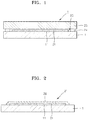
- FIG. 1 is a cross-sectional view of an organic light emitting display device 2 according to an embodiment of the present invention.
- the organic light emitting display device 2 includes an organic emission unit 21 formed on a first surface 11 of a substrate 1, and a sealing substrate 23 for sealing the organic emission unit 21.
- the sealing substrate 23 may be formed of a transparent material to display an image generated by the organic emission unit 21, and to prevent or substantially prevent external air and moisture from penetrating into the organic emission unit 21.
- a space 25 between the substrate 1 and the sealing substrate 23 is sealed by coupling edges of the substrate 1 and the sealing substrate 23 with sealing materials 24.
- the space 25 may be filled with an absorbent or a filler, as will be described later.
- a thin sealing film 26 instead of the sealing substrate 23 may be formed on the organic emission unit 21 to protect the organic emission unit 21 from external air and moisture.
- the thin sealing film 26 may have a structure in which a film formed of an inorganic material (e.g., a silicon oxide or a silicon nitride), and a film formed of an organic material (e.g., epoxy or polyimide) are alternately stacked, but the present invention is not limited thereto. That is, in other embodiments, the thin sealing film 26 may include any thin film type sealing structure.
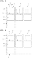
- FIG. 3 is a schematic plan view of an example of the organic emission unit 21 of FIG. 1 or FIG. 2 , according to an example not falling under the scope of the invention.
- a red pixel Pr, a green pixel Pg, and a blue pixel Pb are arranged to be adjacent to one another in the organic emission unit 21.
- Each of the red pixel Pr, the green pixel Pg, and the blue pixel Pb includes a first emission area PA1, a second emission area PA2, and a transmissive area TA.
- the first emission area PA1, the second emission area PA2, and the transmissive area TA are sequentially arranged to be adjacent to each other, as illustrated in FIG. 3 , but the present invention is not limited thereto.
- the transmissive area TA may be disposed above or between the first and second emission areas PA1 and PA2.
- each of the first emission areas PA1 includes a pixel circuit unit PC. Although not shown in FIG. 3 , various wires connected to the pixel circuit unit PC may be disposed to pass through the first emission area PA1 or near the first emission area PA1.
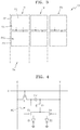
- FIG. 4 is a circuit diagram of the pixel circuit unit PC of FIG. 3 , according to an example not falling under the scope of the invention.
- conductive lines e.g., a scan line S, a data line D, and a Vdd line V which is a power supply voltage line
- various other conductive lines may further be connected to the pixel circuit unit PC according to a structure of the pixel circuit unit PC.
- the pixel circuit unit PC in one embodiment, includes a first thin-film transistor (TFT) T1 connected to the scan line S and the data line D, a second TFT T2 connected to the first TFT T1 and the Vdd line V, and a capacitor Cst connected to the first and second TFTs T1 and T2.
- TFT thin-film transistor
- a gate electrode is connected to the scan line S to receive a scan signal, a first electrode is connected to the data line D, and a second electrode is connected to the capacitor Cst, and a gate electrode of the second TFT T2.
- a first electrode is connected to the Vdd line V and the capacitor Cst, and a second electrode is connected to first electrodes of a first light emitting TFT T3 and a second light emitting TFT T4.
- the first TFT T1 may act as a switching transistor, and the second TFT T2 may act as a driving transistor.
- a second electrode of the first light emitting TFT T3 is electrically connected to a first organic light emitting diode E1
- a second electrode of the second light emitting TFT T4 is electrically connected to a second organic light emitting diode E2.
- the second electrode of the first light emitting TFT T3 and the second electrode of the second light emitting TFT T4 are electrically connected to a first pixel electrode 221 and a second pixel electrode 222 of the organic emission unit 21, respectively.
- Gate electrodes of the first light emitting TFT T3 and the second light emitting TFT T4 are electrically connected to additional emission signal lines (not shown),_respectively.
- the TFTs T1 to T4 are P-type transistors, and, in another embodiment, at least one of the TFTs T1 to T4 may be an N-type transistor.
- Four TFTs and one capacitor are included in the pixel circuit unit PC according to one embodiment, and, in another embodiment, a combination of at least two TFTs and at least one capacitor may further be used according to a structure of the pixel circuit unit PC.
- the pixel circuit unit PC is disposed to overlap with or be contained within the first emission area PA1 and not to overlap with the second emission area PA2.
- top emission of each subpixel occurs in each of the first emission areas PA1. Since the pixel circuit unit PC is disposed in each of the first emission areas PA1 where top emission occurs, and a conductive pattern of the pixel circuit unit PC, which is an important factor that can degrade transmissivity, is not disposed in the transmissive area TA, the transmission of the transmissive area TA is greatly improved.
- the pixel circuit unit PC overlaps with the first pixel electrode 221 to be hidden by the first pixel electrode 221, but does not overlap with the second pixel electrode 222.
- At least one of the conductive lines including the scan line S, the data line D, and the Vdd line V may be disposed to cross the first pixel electrode 221. Since transmissivity is decreased less by the conductive lines than by the pixel circuit unit PC, according to one embodiment, all of the conductive lines may be arranged adjacent to the first pixel electrode 221.
- the first pixel electrode 221 may include a reflective layer formed of conductive metal that reflects light, as described later herein, and the pixel circuit unit PC hidden by the first pixel electrode 221 may be screened by the first pixel electrode 221.
- each of the second emission areas PA2 bottom emission of each subpixel occurs. Since the pixel circuit unit PC is not disposed in each of the second emission areas PA2 where bottom emission occurs, the efficiency of bottom emission is not degraded.
- image information received via the data line D is displayed on the first organic light emitting diode E1 when the first light emitting TFT T3 is “off,” and is displayed on the second organic light emitting diode E2 when the second light emitting TFT T4 is “off.”
- different images may be displayed on the first organic light emitting diode E1 and the second organic light emitting diode E2.
- dual emission may be performed based on time-division driving in such a manner that the left and right sides of an image displayed on a surface on which top emission occurs without being reversed relative to those of an image displayed on a surface on which bottom emission occurs.
- the pixel circuit unit PC includes a first pixel circuit unit PC1 being electrically connected to the first pixel electrode 221, and a second pixel circuit unit PC2 being electrically connected to the second pixel electrode 222.
- the first pixel circuit unit PC1 and the second pixel circuit unit PC2 are individually operated.
- the first pixel circuit unit PC1 and the second pixel circuit unit PC2 may have a structure of a general pixel circuit unit.
- a plurality of separate transmissive areas TA may be formed to correspond to a red pixel Pr, a green pixel Pg, and a blue pixel Pb, respectively, but the present invention is not limited thereto.
- a single transmissive area TA may be formed to correspond to all of the red pixel Pr, the green pixel Pg, and the blue pixel Pb.
- the area of the single transmissive area TA is greater than the sum of the areas of the separate transmissive areas TA of the previously described embodiments, thereby increasing the transmissivity of external light.
- FIG. 7 is a cross-sectional view of a pixel of the organic emission unit 21, according to an embodiment of the present invention.
- a buffer film 211 is formed on the first surface 11 of the substrate 1, and the first light emitting TFT T3 and the second light emitting TFT T4 are formed on the buffer film 211.
- FIG. 7 illustrates only the first light emitting TFT T3 and the second light emitting TFT T4 for reasons of clarity, all the elements of the pixel circuit unit PC illustrated in FIG. 4 may be formed on the buffer film 211.
- a first semiconductor active layer 212a and a second semiconductor active layer 212b are formed on the buffer film 211.
- the buffer film 211 prevents or substantially prevents impurity elements from penetrating into the organic emission unit 21 and planarizes a surface of the organic emission unit 21.
- the buffer film 211 may be formed of any of various materials to perform the functions described above.
- the buffer film 211 may be formed of an inorganic material (e.g., a silicon oxide, a silicon nitride, a silicon oxynitride, an aluminum oxide, an aluminum nitride, a titanium oxide, or a titanium nitride), an organic material (e.g., polyimide, polyester, or acryl), or a stack of these materials.
- the buffer film 211 may be omitted.
- the first and second semiconductor active layers 212a and 212b may be formed of polycrystal silicon, but are not limited thereto, and, in another embodiment, for example, may be formed of an oxide semiconductor.
- the first and second semiconductor active layers 212a and 212b may be G-I-Z-0 layers [(In 2 O 3 ) a (Ga 2 O 3 ) b (ZnO) c layer], wherein a, b, and c are integers that respectively satisfy a ⁇ 0, b ⁇ 0, and c>0.
- a gate insulating film 213 covering the first and second semiconductor active layers 212a and 212b is formed on the buffer film 211, and first and second gate electrodes 214a and 214b are formed on the gate insulating film 213.
- an interlayer insulating film 215 is formed on the gate insulating film 213 to cover the first and second gate electrodes 214a and 214b.
- a first source electrode 216a and a first drain electrode 217a, and a second source electrode 216b and a second drain electrode 217b are formed on the interlayer insulating film 215 to be connected to the first semiconductor active layer 212a and the second semiconductor active layer 212b through contact holes, respectively.
- the scan line S in one embodiment, may be concurrently or simultaneously formed with the first and second gate electrodes 214a and 214b.
- the data line D and the Vdd line V in one embodiment, may be concurrently or simultaneously formed with the first source electrode 216a and the second source electrode 216b.
- first and second light emitting TFTs TR3 and TR4 are not limited thereto, and any of various types of TFT structures may be employed.
- a passivation film 218 is formed to cover the first and second light emitting TFTs T3 and T4.
- the passivation film 218 may be a single layer or multiple layers of insulating film.
- the passivation film 218 may be formed of an inorganic material and/or an organic material.
- the first pixel electrode 221 covering the first and second light emitting TFTs T3 and T4 may be formed on the passivation film 218.
- the first pixel electrode 221 is connected to the first drain electrode 217a of the first light emitting TFT T3 through a via hole formed in the passivation film 218.
- the second pixel electrode 222 in one embodiment, is formed on the passivation film 218 adjacent to the first pixel electrode 221.
- the first pixel electrode 221 and the second pixel electrode 222 are separated from each other.
- the second pixel electrode 222 is connected to the second drain electrode 217b of the second light emitting TFT T4 through a via hole formed in the passivation film 218.
- a pixel defining film 219 covering edges of the first pixel electrode 221 and the second pixel electrode 222 is formed on the passivation film 218.
- a first organic layer 223 is formed on the first pixel electrode 221, and a first opposing electrode 224 is formed to cover the first organic layer 223.
- a second organic layer 223' is formed on the second pixel electrode 222, and a second opposing electrode 225 is formed to cover the second organic layer 223'.
- the first opposing electrode 224 and the second opposing electrode 225 may be electrically connected to each other, as illustrated in FIG. 7 .
- the same material may be used to form the first organic layer 223 and the second organic layer 223'.
- the first organic layer 223 and the second organic layer 223' may each be a low-molecular weight organic layer or a polymer organic layer having a high molecular weight.
- the first organic layer 223 and the second organic layer 223' are each a low-molecular weight organic film, and may be formed by stacking a hole injection layer (HIL), a hole transport layer (HTL), an emission layer (EML), an electron transport layer (ETL), and an electron injection layer (EIL) in a single structure or a composite structure, and may be formed of any of various materials, such as copper phthalocyanine (CuPc), N,N'-Di(naphthalene-1-yl)-N,N'-diphenyl-benzidine (NPB), or tris-8-hydroxyquinoline aluminum (Alq3).
- the low-molecular weight organic layer may be formed by vacuum deposition.
- the EML may be individually formed for each pixel, and the HIL, the HTL, the ETL, and the EIL may be common layers that are used in the pixels.
- the first pixel electrode 221 and the second pixel electrode 222 may function as anode electrodes, and the first opposing electrode 224 and the second opposing electrode 225 may function as cathode electrodes, or vice versa.
- the first pixel electrode 221 may have a size corresponding to that of the first emission area PA1 of each pixel, and the second pixel electrode 222 may have a size corresponding to that of the second emission area PA2 of each pixel.
- a common voltage may be applied to the first and second opposing electrodes 224 and 225 of all of the pixels of the organic emission layer 21.
- the passivation film 218, the gate insulating film 213, the interlayer insulating film 215, and the pixel defining film 219 may be formed as transparent insulating films, but the present invention is not limited thereto.
- the substrate 1 may have a transmissivity less than or equal to a total transmissivity of the transparent insulating films.
- FIG. 8A is a schematic cross-sectional view of a first organic light emitting diode in the first emission area PA1 of FIG. 7 , according to an embodiment of the present invention.
- FIG. 8B is a schematic cross-sectional view of a second organic light emitting diode in the second emission area PA2 of FIG. 7 , according to an embodiment of the present invention.
- the first pixel electrode 221 may be an electrode including a reflective layer, and the first opposing electrode 224 may be a semi-transparent and semi-reflective electrode. Accordingly, the first emission area PA1 may be a top emission type area in which an image is displayed toward the first opposing electrode 224.
- the first pixel electrode 221 is a reflective electrode, and the pixel circuit unit PC disposed under the first pixel electrode 221 is covered by the first pixel electrode 221.
- the first light emitting TFT T3 and the second light emitting TFT T4 under the first pixel electrode 221 are not visible at an outer side above the first opposing electrode 224.
- the first pixel electrode 221 is a reflective electrode, light is emitted only toward a user, thereby preventing or reducing optical loss in a direction opposite to the user.
- the second pixel electrode 222 is a transparent electrode, and the second opposing electrode 225 is a reflective electrode.
- the second emission area PA2 is a bottom emission type area in which an image is displayed toward the second pixel electrode 222.
- the first pixel electrode 221, in one embodiment, may be a stacked structure of a first transparent conductive film 221a, a reflective layer 221b, and a second transparent conductive film 221c.
- the first transparent conductive film 221a and the second transparent conductive film 221c may each include an oxide having a high work function, such as ITO, IZO, ZnO, or In 2 O 3 .
- the reflective layer 221b may be formed of a metal having a low work function, such as silver (Ag), magnesium (Mg), aluminum (Al), platinum (Pt), palladium (Pd), gold (Au), nickel (Ni), neodymium (Nd), iridium (Ir), chromium (Cr), lithium (Li), calcium (Ca), ytterbium (Yb), or an alloy thereof, as described above.
- a metal having a low work function such as silver (Ag), magnesium (Mg), aluminum (Al), platinum (Pt), palladium (Pd), gold (Au), nickel (Ni), neodymium (Nd), iridium (Ir), chromium (Cr), lithium (Li), calcium (Ca), ytterbium (Yb), or an alloy thereof, as described above.
- the first organic layer 223, in one embodiment, is a stacked structure of a first functional layer 223a, a first emission layer 223b, and a second functional layer 223c formed on the first pixel electrode 221.
- the first opposing electrode 224 is formed on the first organic layer 223.
- the first functional layer 223a may include an HIL and a HTL
- the second functional layer 223c may include an EIL and an ETL.
- the first opposing electrode 224 may be formed of a metal having a low work function, such as silver (Ag), magnesium (Mg), aluminum (Al), platinum (Pt), palladium (Pd), gold (Au), nickel (Ni), neodymium (Nd), iridium (Ir), chromium (Cr), lithium (Li), calcium (Ca), ytterbium (Yb), or an alloy thereof.
- the first opposing electrode 224 may be a thin film having a high transmissivity, and may be formed having a thickness of about 100 to 300 ⁇ .
- a distance between a surface of the reflective layer 221b and the first opposing electrode 224 may be adjusted to cause optical resonance to occur, based on a wavelength of light emitted from the first emission layer 223b.
- the distance may be different for red, green, and blue pixels.
- the distance may be adjusted by further forming an auxiliary layer on the first functional layer 223a and/or the second functional layer 223c to a thickness according to the color of a pixel.
- the first emission area PA1 having the above-described structure is a top emission type area in which an image is displayed toward the opposing electrode 224, and light extraction efficiency may be increased or maximized by adjusting the distance between a surface of the reflective layer 221b and the first opposing electrode 224.
- the second pixel electrode 222 is formed of a transparent conductive material having a low reflectivity.
- the second pixel electrode 222 may be formed concurrently or simultaneously with at least one of the first transparent conductive film 221a and the second transparent conductive film 221c included in the first pixel electrode 221.
- the present invention is not limited thereto, and a second pixel electrode 222' according to another embodiment of the present invention may be a stacked structure of a first transparent conductive film 222a, a reflective layer 222b, and a second transparent conductive film 222c, as shown in FIG. 8C .
- the first transparent conductive film 222a and the second transparent conductive film 222c may include an oxide having a high work function, such as ITO, IZO, ZnO, or In 2 O 3 .
- the reflective layer 222b may have a semi-transparent characteristic by being formed of a thin film metal, such as silver (Ag), magnesium (Mg), aluminum (Al), platinum (Pt), palladium (Pd), gold (Au), nickel (Ni), neodymium (Nd), iridium (Ir), chromium (Cr), lithium (Li), calcium (Ca), ytterbium (Yb), or an alloy thereof.
- the first transparent conductive film 222a, the reflective layer 222b, and the second transparent conductive film 222c of the second pixel electrode 222' may be formed concurrently or simultaneously with the first transparent conductive film 221a, the reflective layer 221b, and the second transparent conductive film 221c of the first pixel electrode 221, respectively.
- the second organic layer 223' in one embodiment, is a stacked structure including a third functional layer 223a', a second emission layer 223b', and a fourth functional layer 223c' formed on the second pixel electrode 222.
- the second opposing electrode 225 is formed on the second organic layer 223'.
- the third functional layer 223a' and the fourth functional layer 223c' may extend from the first functional layer 223a and the second functional layer 223c, respectively.
- the second emission layer 223b' may extend from the first emission layer 223b.
- the second emission area PA2 is a bottom emission type area in which an image is displayed toward the second pixel electrode 222
- the second opposing electrode 225 may include a semi-transmissive film 225a and a metal film 225b.
- the semi-transmissive film 225a may be formed of a material used to form the first opposing electrode 224, and may extend from the first opposing electrode 224.
- the metal film 225b may be stacked on the semi-transmissive film 225a and may function as a reflective layer.
- the metal film 225b may be formed of a metal having a low work function, such as silver (Ag), magnesium (Mg), aluminum (Al), platinum (Pt), palladium (Pd), gold (Au), nickel (Ni), neodymium (Nd), iridium (Ir), chromium (Cr), lithium (Li), calcium (Ca), ytterbium (Yb), or an alloy thereof.
- the metal film 225b in one embodiment, may be formed to be thicker than the semi-transmissive film 225a so as to increase the reflectivity of light emitted from the second organic layer 223' and reduce a voltage drop in the second opposing electrode 225.
- the metal film 225b may be formed before the semi-transmissive film 225a is formed.
- the second opposing electrode 225' has a structure in which the metal film 225b and the semi-transmissive film 225a are sequentially stacked.
- the semi-transmissive film 225a of the second opposing electrode 225 may be integrally formed with the first opposing electrode 224.
- a second opposing electrode 225" may include only the metal film 225b if needed, as illustrated in FIG. 8E .
- the above various embodiments of the structure of the second opposing electrode 225' and 225" may also be applied with the structure of the second pixel electrode 222' illustrated in FIG. 8C .
- FIG. 7 illustrates that the second opposing electrode 225 is a stacked structure of the semi-transmissive film 225a and the metal film 225b as illustrated in FIG. 8B
- the present invention is not limited thereto, and, in other embodiments, the second emission area PA2 shown in FIG. 7 may include the second opposing electrode 225' that is a stacked structure of the metal film 225b and the semi-transmissive film 225a, as illustrated in FIG. 8D , or may include the second opposing electrode 225" that is only the metal film 225b, as illustrated in FIG. 8E .
- the metal film 225b in one embodiment, may be formed not to extend at least to the transmissive area TA, as illustrated in FIG. 7 .
- a transparent window 230 is formed in the transmissive area TA to greatly increase the transmittance of external light through the transmissive area TA, as illustrated in FIG. 7 .
- the transparent window 230 may have an area corresponding to the transmissive area TA.
- a first transparent window 231 may be formed by forming an aperture in the first opposing electrode 224 and the second opposing electrode 225 at a location corresponding to the transmissive area TA such that the first opposing electrode 224 and the second opposing electrode 225 are not formed in the transmissive area TA.
- the first transparent window 231 improves the transmittance of external light through the transmissive area TA.
- an extended opposing electrode 226 may be formed in the transmissive area TA, as illustrated in FIG. 9 .
- the extended opposing electrode 226 may be formed of a material used to form the first opposing electrode 224 and the semi-transmissive film 225a, and may extend from the semi-transmissive film 225a.
- the metal film 225b may have apertures corresponding to the first emission area PA1 and the transmissive area TA as illustrated in FIG. 7 or FIG. 9 .
- the aperture in the metal film 225b corresponding to the transmissive area TA may be formed to correspond to the first transparent window 231.
- FIG. 10 is a cross-sectional view of an organic emission unit according to another embodiment of the present invention.
- a second transparent window 232 is formed in the pixel defining film 219.
- the second transparent window 232 may be connected to the first transparent window 231, such as that shown in FIG. 7 , thus forming the transparent window 230.
- the second transparent window 232 is shown formed only in the pixel defining film 219, but the present invention is not limited thereto, and, in another embodiment, the second transparent window 232 may be formed in at least one of the insulating films formed in the transmissive area TA.
- the second transparent window 232 increases the transmissivity of the transmissive area TA, and may also prevent or reduce optical interference, degradation in color purity, and a change in color, caused by multilayered transparent insulating films.
- the transparent window 230 may include only the second transparent window 232, and a first transparent window which is an aperture may not be formed in the extended opposing electrode 226.
- a plurality of the transparent windows each corresponding to the shape of the transmissive area TA may be formed separately for the red pixel Pr, the green pixel Pg, and the blue pixel Pb, as illustrated in FIG. 3 .
- a single transmissive area TA corresponds to all of the red pixel Pr, the green pixel Pg, and the blue pixel Pb, as illustrated in FIG. 6 , and a transparent window may be formed for all of the red pixel Pr, the green pixel Pg, and the blue pixel Pb.
Description
- The present invention relates to organic light emitting display devices.
- Organic light emitting display devices generally have wide viewing angles, high contrast ratios, short response times, and reduced power consumption, and thus may be used across a variety of applications, such as personal portable devices (e.g., MP3 players and mobile phones), or large-screen displays (e.g., television sets).
- An organic light emitting display device has self-emitting characteristics, and weight and thickness of the organic light emitting display device can be reduced since the organic light emitting display device does not require an additional light source, unlike a liquid crystal display (LCD) device.
- Also, an organic light emitting display device can be manufactured as a transparent display device by including transparent thin-film transistors (TFTs) and transparent organic light emitting diodes.
- In a transparent display device, when the device is in an off-state, an image of an object or an image positioned at a side of the device opposite to a user is transmitted to the user through not only patterns of organic light emitting diodes, TFTs and various wires but also through spaces between the patterns. However, the patterns of organic light emitting diodes, TFTs, and wires do not have a high transmissivity, and the spaces between the patterns are not very wide. Thus, the transmissivity of the entire transparent display device is typically not great.
Therefore, a distorted image may be transmitted to the user due to the patterns of organic light emitting diodes, TFTs, and wires. The reason for this is because gaps between the patterns are typically merely a few hundred nanometers, that is, almost equal to the wavelengths of visible light, thus causing light to scatter as it passes through the patterns. - An organic light emitting display device may be produced to be a dual-sided light emitting display device, compared to an LCD device. However, in the existing dual-sided light emitting display device, the same image is displayed on both surfaces thereof. Thus, the left and right sides of the image displayed on one of the surfaces are reversed relative to those of the image displayed on the other surface.
- In addition, a dual-sided light emitting display device may be manufactured by separately manufacturing two organic light emitting display devices and binding them together. However, in this case, the dual-sided light emitting display device cannot be embodied as a transparent display device.
-
US 2011/148944 A1 relates to a display device including a light emitting functional layer disposed between a first and second substrates. -
US 2009/051285 A1 relates to an organic electroluminescence display device. - According to an aspect of the current invention, there is provided an organic light emitting display according to
claim 1. - According to an aspect of embodiments of the present invention, in an organic light emitting display device, transparent transmissive areas are formed by improving the transmissivity of the transmissive areas, and dual emission occurs.
- According to another aspect of embodiments of the present invention, a transparent organic light emitting display device prevents or reduces distortion of an image transmitted therethrough by preventing or substantially preventing light from scattering during image display.
- According to an embodiment of the present invention, an organic light emitting display device includes: a first emission area including a first organic light emitting diode; a second emission area arranged adjacent to the first emission area and not overlapping with the first emission area, the second emission area including a second organic light emitting diode; a pixel circuit unit electrically connected to the first organic light emitting diode and the second organic light emitting diode; and a transmissive area adjacent to the first and second emission areas and not overlapping with the first and second emission areas, the transmissive area configured to transmit external light therethrough.
- The pixel circuit units are arranged to overlap with the first emission area and not to overlap with the second emission area. The first organic light emitting diode includes a first pixel electrode configured to reflect light.
- The second organic light emitting diode includes a second pixel electrode configured to transmit light therethrough.
- The pixel circuit units individually drive the first organic light emitting diode and the second organic light emitting diode.
- The pixel circuit unit may include a first light emitting thin film transistor (TFT) electrically connected to the first organic light emitting diode; and a second light emitting TFT electrically connected to the second organic light emitting diode.
- The organic light emitting display device may further include a data line, a scan line, and a power supply source line for supplying a data signal, a scan signal, and power to the pixel circuit unit, respectively. The pixel circuit unit may include a first TFT, a second TFT, and a capacitor. In the first TFT, a gate electrode may be electrically connected to the scan line, a first electrode may be electrically connected to the data line, and a second electrode may be electrically connected to a gate electrode of the second TFT and the capacitor. In the second TFT, a first electrode may be electrically connected to the power supply source line and the capacitor, and a second electrode may be electrically connected to the first and second light emitting TFTs.
- In the first light emitting TFT, a first electrode may be electrically connected to the second TFT, and a second electrode may be electrically connected to the first organic light emitting diode. In the second light emitting TFT, a first electrode may be electrically connected to the second TFT, and a second electrode may be electrically connected to the second organic light emitting diode.
- The first organic light emitting diode and the second organic light emitting diode may emit a same color of light.
- The organic light emitting display device further includes a plurality of transparent windows arranged in the transmissive areas.
- The organic light emitting display device includes: a substrate; a plurality of pixels formed on the substrate, each of the plurality of pixels including a first emission area, a second emission area, a transmissive area configured to transmit external light therethrough, and a pixel circuit unit; a plurality of first pixel electrodes, each being arranged in the first emission area of one of the plurality of pixels and electrically connected to the pixel circuit unit of the one of the plurality of pixels, each of the plurality of first pixel electrodes including a transparent conductive film and a reflective layer; a plurality of second pixel electrodes, each being arranged in the second emission area of a respective one of the plurality of pixels, electrically connected to the pixel circuit unit of the respective one of the plurality of pixels, and arranged apart from the plurality of first pixel electrodes, each of the plurality of second pixel electrodes including a transparent conductive film or a semi-transmissive layer; a first opposing electrode facing the plurality of first pixel electrodes; a second opposing electrode facing the plurality of second pixel electrodes; a first organic layer between the plurality of first pixel electrodes and the first opposing electrode, the first organic layer including a first emission layer; and a second organic layer between the plurality of second pixel electrodes and the second opposing electrode, the second organic layer including a second emission layer.
- The first and second opposing electrodes may be electrically connected to each other.
- The first opposing electrode may be configured to transmit light therethrough.
- The first opposing electrode and the second opposing electrode may each include at least one metal selected from the group consisting of silver (Ag), magnesium (Mg), aluminum (Al), platinum (Pt), palladium (Pd), gold (Au), nickel (Ni), neodymium (Nd), iridium (Ir), chromium (Cr), lithium (Li), calcium (Ca), and ytterbium (Yb).
- Each of the pixel circuit units is arranged to overlap with one of the plurality of first pixel electrodes and not to overlap with any of the plurality of second pixel electrodes.
- Each of the pixel circuit units may include a first light emitting thin film transistor (TFT) electrically connected to one of the plurality of first pixel electrodes; and a second light emitting TFT electrically connected to one of the plurality of second pixel electrodes.
- The organic light emitting display device may further include a data line, a scan line, and a power supply source line for supplying a data signal, a scan signal, and power to the pixel circuit unit, respectively. The pixel circuit unit may include a first TFT, a second TFT, and a capacitor. In the first TFT, a gate electrode may be electrically connected to the scan line, a first electrode may be electrically connected to the data line, and a second electrode may be electrically connected to a gate electrode of the second TFT and the capacitor. In the second TFT, a first electrode may be electrically connected to the power supply source line and the capacitor, and a second electrode may be electrically connected to the first and second light emitting TFTs.
- In the first light emitting TFT, a first electrode may be electrically connected to the second TFT and a second electrode may be electrically connected to a first organic light emitting diode of a pixel of the plurality of pixels, and, in the second light emitting TFT, a first electrode may be electrically connected to the second TFT and a second electrode may be electrically connected to a second organic light emitting diode of the pixel of the plurality of pixels.
- Each of the pixel circuit units includes a first pixel circuit unit electrically connected to one of the plurality of first pixel electrodes; and a second pixel circuit unit electrically connected to one of the plurality of second pixel electrodes, and being operated independently with the first pixel circuit unit.
- The first pixel circuit unit and the second pixel circuit unit are arranged to overlap with the first emission area and not to overlap with the second emission area.
- The transmissive areas of at least two adjacent pixels from among the plurality of pixels may be integrally formed.
- The organic light emitting display device further includes a plurality of transparent windows arranged in the transmissive areas.
- The transparent windows of at least two adjacent pixels from among the plurality of pixels may be integrally formed.
- The second opposing electrode includes a reflective metal film, and the reflective metal film may include a plurality of apertures, each corresponding to one of the first emission areas and one of the plurality of the transparent windows.
- According to an aspect of embodiments of the present invention, a transparent organic light emitting display device may be manufactured by improving the transmissivity of external light and to allow dual emission to occur in the transparent organic light emitting display device.
- According to another aspect of embodiments of the present invention, a transparent organic light emitting display device is capable of preventing or reducing distortion of an image transmitted therethrough by eliminating or substantially eliminating light-scattering during image display.
- The above and other features and aspects of the present invention will become more apparent by describing in further detail some exemplary embodiments thereof with reference to the attached drawings, in which:
-
FIG. 1 is a cross-sectional view of an organic light emitting display device according to an embodiment of the present invention; -
FIG. 2 is a cross-sectional view of an organic light emitting display device according to another embodiment of the present invention; -
FIG. 3 is a schematic plan view of an organic emission unit not falling under the invention; -
FIG. 4 is a circuit diagram of a pixel circuit unit of the organic emission unit ofFIG. 3 , -
FIG. 5 is a schematic plan view of an organic emission unit according to an embodiment of the present invention; -
FIG. 6 is a schematic plan view of an organic emission unit not falling under the invention; -
FIG. 7 is a cross-sectional view of the organic emission unit ofFIG. 3 , according to an embodiment of the present invention; -
FIG. 8A is a schematic cross-sectional view of a first organic light emitting diode in a first emission area of the organic emission unit ofFIG. 7 , according to an embodiment of the present invention; -
FIG. 8B is a schematic cross-sectional view of a second organic light emitting diode in a second emission area of the organic emission unit ofFIG. 7 , according to an embodiment of the present invention; -
FIG. 8C is a schematic cross-sectional view of a second organic light emitting diode in a second emission area of an organic emission unit, according to another embodiment of the present invention; -
FIG. 8D is a schematic cross-sectional view of a second organic light emitting diode in a second emission area of an organic emission unit, according to another embodiment of the present invention; -
FIG. 8E is a schematic cross-sectional view of a second organic light emitting diode in a second emission area of an organic emission unit, according to another embodiment of the present invention; -
FIG. 9 is a cross-sectional view of an organic emission unit according to another embodiment of the present invention; and -
FIG. 10 is a cross-sectional view of an organic emission unit according to another embodiment of the present invention. -
FIG. 1 is a cross-sectional view of an organic light emittingdisplay device 2 according to an embodiment of the present invention. Referring toFIG. 1 , the organic light emittingdisplay device 2 includes anorganic emission unit 21 formed on afirst surface 11 of asubstrate 1, and a sealingsubstrate 23 for sealing theorganic emission unit 21. - The sealing
substrate 23 may be formed of a transparent material to display an image generated by theorganic emission unit 21, and to prevent or substantially prevent external air and moisture from penetrating into theorganic emission unit 21. - A
space 25 between thesubstrate 1 and the sealingsubstrate 23 is sealed by coupling edges of thesubstrate 1 and the sealingsubstrate 23 with sealingmaterials 24. Thespace 25 may be filled with an absorbent or a filler, as will be described later. - As illustrated in
FIG. 2 , in an organic light emitting display device 2' according to another embodiment of the present invention, athin sealing film 26 instead of the sealingsubstrate 23 may be formed on theorganic emission unit 21 to protect theorganic emission unit 21 from external air and moisture. In one embodiment, thethin sealing film 26 may have a structure in which a film formed of an inorganic material (e.g., a silicon oxide or a silicon nitride), and a film formed of an organic material (e.g., epoxy or polyimide) are alternately stacked, but the present invention is not limited thereto. That is, in other embodiments, thethin sealing film 26 may include any thin film type sealing structure. -
FIG. 3 is a schematic plan view of an example of theorganic emission unit 21 ofFIG. 1 or FIG. 2 , according to an example not falling under the scope of the invention. Referring toFIG. 3 , a red pixel Pr, a green pixel Pg, and a blue pixel Pb are arranged to be adjacent to one another in theorganic emission unit 21. - Each of the red pixel Pr, the green pixel Pg, and the blue pixel Pb includes a first emission area PA1, a second emission area PA2, and a transmissive area TA.
- In one embodiment, in each of the red pixel Pr, the green pixel Pg, and the blue pixel Pb, the first emission area PA1, the second emission area PA2, and the transmissive area TA are sequentially arranged to be adjacent to each other, as illustrated in
FIG. 3 , but the present invention is not limited thereto. For example, in another embodiment, the transmissive area TA may be disposed above or between the first and second emission areas PA1 and PA2. - Referring to
FIG. 3 , each of the first emission areas PA1 includes a pixel circuit unit PC. Although not shown inFIG. 3 , various wires connected to the pixel circuit unit PC may be disposed to pass through the first emission area PA1 or near the first emission area PA1. -
FIG. 4 is a circuit diagram of the pixel circuit unit PC ofFIG. 3 , according to an example not falling under the scope of the invention. Referring toFIG. 4 , conductive lines (e.g., a scan line S, a data line D, and a Vdd line V which is a power supply voltage line) are electrically connected to the pixel circuit unit PC. Although not shown, various other conductive lines may further be connected to the pixel circuit unit PC according to a structure of the pixel circuit unit PC. - The pixel circuit unit PC, in one embodiment, includes a first thin-film transistor (TFT) T1 connected to the scan line S and the data line D, a second TFT T2 connected to the first TFT T1 and the Vdd line V, and a capacitor Cst connected to the first and second TFTs T1 and T2.
- In the first TFT T1, a gate electrode is connected to the scan line S to receive a scan signal, a first electrode is connected to the data line D, and a second electrode is connected to the capacitor Cst, and a gate electrode of the second TFT T2.
- In the second TFT T2, a first electrode is connected to the Vdd line V and the capacitor Cst, and a second electrode is connected to first electrodes of a first light emitting TFT T3 and a second light emitting TFT T4.
- In one embodiment, the first TFT T1 may act as a switching transistor, and the second TFT T2 may act as a driving transistor.
- In one embodiment, a second electrode of the first light emitting TFT T3 is electrically connected to a first organic light emitting diode E1, and a second electrode of the second light emitting TFT T4 is electrically connected to a second organic light emitting diode E2. Thus, referring to
FIGS. 3 and 4 , the second electrode of the first light emitting TFT T3 and the second electrode of the second light emitting TFT T4 are electrically connected to afirst pixel electrode 221 and asecond pixel electrode 222 of theorganic emission unit 21, respectively. - Gate electrodes of the first light emitting TFT T3 and the second light emitting TFT T4 are electrically connected to additional emission signal lines (not shown),_respectively.
- In one embodiment, the TFTs T1 to T4 are P-type transistors, and, in another embodiment, at least one of the TFTs T1 to T4 may be an N-type transistor. Four TFTs and one capacitor are included in the pixel circuit unit PC according to one embodiment, and, in another embodiment, a combination of at least two TFTs and at least one capacitor may further be used according to a structure of the pixel circuit unit PC.
- According to the present invention, the pixel circuit unit PC is disposed to overlap with or be contained within the first emission area PA1 and not to overlap with the second emission area PA2.
- As will be described below, top emission of each subpixel occurs in each of the first emission areas PA1. Since the pixel circuit unit PC is disposed in each of the first emission areas PA1 where top emission occurs, and a conductive pattern of the pixel circuit unit PC, which is an important factor that can degrade transmissivity, is not disposed in the transmissive area TA, the transmission of the transmissive area TA is greatly improved.
- In other words, the pixel circuit unit PC overlaps with the
first pixel electrode 221 to be hidden by thefirst pixel electrode 221, but does not overlap with thesecond pixel electrode 222. - In one embodiment, at least one of the conductive lines including the scan line S, the data line D, and the Vdd line V may be disposed to cross the
first pixel electrode 221. Since transmissivity is decreased less by the conductive lines than by the pixel circuit unit PC, according to one embodiment, all of the conductive lines may be arranged adjacent to thefirst pixel electrode 221. Thefirst pixel electrode 221 may include a reflective layer formed of conductive metal that reflects light, as described later herein, and the pixel circuit unit PC hidden by thefirst pixel electrode 221 may be screened by thefirst pixel electrode 221. - In each of the second emission areas PA2, bottom emission of each subpixel occurs. Since the pixel circuit unit PC is not disposed in each of the second emission areas PA2 where bottom emission occurs, the efficiency of bottom emission is not degraded.
- According to the above-described structure of the pixel circuit unit PC, image information received via the data line D is displayed on the first organic light emitting diode E1 when the first light emitting TFT T3 is "off," and is displayed on the second organic light emitting diode E2 when the second light emitting TFT T4 is "off." Thus, different images may be displayed on the first organic light emitting diode E1 and the second organic light emitting diode E2. Accordingly, dual emission may be performed based on time-division driving in such a manner that the left and right sides of an image displayed on a surface on which top emission occurs without being reversed relative to those of an image displayed on a surface on which bottom emission occurs. However, if the same switching signal is supplied to the first light emitting TFT T3 and the second light emitting TFT T4 to which the same data signal is input, then the left and right sides of an image displayed on a front surface are reversed relative to those of an image displayed on a bottom surface. As described above, it is possible to display an image on the first organic light emitting diode E1 and the second organic light emitting diode E2 that share the basic structure of the pixel circuit unit PC, in various manners.
- Referring to
FIG. 5 , according to the present invention, the pixel circuit unit PC includes a first pixel circuit unit PC1 being electrically connected to thefirst pixel electrode 221, and a second pixel circuit unit PC2 being electrically connected to thesecond pixel electrode 222. The first pixel circuit unit PC1 and the second pixel circuit unit PC2 are individually operated. The first pixel circuit unit PC1 and the second pixel circuit unit PC2 may have a structure of a general pixel circuit unit. - Referring to
FIG. 3 orFIG. 5 , a plurality of separate transmissive areas TA may be formed to correspond to a red pixel Pr, a green pixel Pg, and a blue pixel Pb, respectively, but the present invention is not limited thereto. For example, referring toFIG. 6 , a single transmissive area TA may be formed to correspond to all of the red pixel Pr, the green pixel Pg, and the blue pixel Pb. In this case, the area of the single transmissive area TA is greater than the sum of the areas of the separate transmissive areas TA of the previously described embodiments, thereby increasing the transmissivity of external light. -
FIG. 7 is a cross-sectional view of a pixel of theorganic emission unit 21, according to an embodiment of the present invention. In theorganic emission unit 21, according to an embodiment of the present invention, abuffer film 211 is formed on thefirst surface 11 of thesubstrate 1, and the first light emitting TFT T3 and the second light emitting TFT T4 are formed on thebuffer film 211. AlthoughFIG. 7 illustrates only the first light emitting TFT T3 and the second light emitting TFT T4 for reasons of clarity, all the elements of the pixel circuit unit PC illustrated inFIG. 4 may be formed on thebuffer film 211. - In one embodiment, a first semiconductor
active layer 212a and a second semiconductoractive layer 212b are formed on thebuffer film 211. - The
buffer film 211 prevents or substantially prevents impurity elements from penetrating into theorganic emission unit 21 and planarizes a surface of theorganic emission unit 21. Thebuffer film 211 may be formed of any of various materials to perform the functions described above. For example, thebuffer film 211 may be formed of an inorganic material (e.g., a silicon oxide, a silicon nitride, a silicon oxynitride, an aluminum oxide, an aluminum nitride, a titanium oxide, or a titanium nitride), an organic material (e.g., polyimide, polyester, or acryl), or a stack of these materials. In another embodiment, thebuffer film 211 may be omitted. - The first and second semiconductor
active layers active layers - In one embodiment, a
gate insulating film 213 covering the first and second semiconductoractive layers buffer film 211, and first andsecond gate electrodes gate insulating film 213. - In one embodiment, an
interlayer insulating film 215 is formed on thegate insulating film 213 to cover the first andsecond gate electrodes first source electrode 216a and afirst drain electrode 217a, and asecond source electrode 216b and asecond drain electrode 217b are formed on theinterlayer insulating film 215 to be connected to the first semiconductoractive layer 212a and the second semiconductoractive layer 212b through contact holes, respectively. - The scan line S, in one embodiment, may be concurrently or simultaneously formed with the first and
second gate electrodes first source electrode 216a and thesecond source electrode 216b. - However, the structures of the first and second light emitting TFTs TR3 and TR4 are not limited thereto, and any of various types of TFT structures may be employed.
- In one embodiment, a
passivation film 218 is formed to cover the first and second light emitting TFTs T3 and T4. Thepassivation film 218 may be a single layer or multiple layers of insulating film. Thepassivation film 218 may be formed of an inorganic material and/or an organic material. - Referring to
FIG. 7 , thefirst pixel electrode 221 covering the first and second light emitting TFTs T3 and T4 may be formed on thepassivation film 218. Thefirst pixel electrode 221 is connected to thefirst drain electrode 217a of the first light emitting TFT T3 through a via hole formed in thepassivation film 218. - The
second pixel electrode 222, in one embodiment, is formed on thepassivation film 218 adjacent to thefirst pixel electrode 221. Thefirst pixel electrode 221 and thesecond pixel electrode 222 are separated from each other. Thesecond pixel electrode 222 is connected to thesecond drain electrode 217b of the second light emitting TFT T4 through a via hole formed in thepassivation film 218. - In one embodiment, a
pixel defining film 219 covering edges of thefirst pixel electrode 221 and thesecond pixel electrode 222 is formed on thepassivation film 218. - A first
organic layer 223 is formed on thefirst pixel electrode 221, and a first opposingelectrode 224 is formed to cover the firstorganic layer 223. - A second organic layer 223' is formed on the
second pixel electrode 222, and a secondopposing electrode 225 is formed to cover the second organic layer 223'. - The first
opposing electrode 224 and the second opposingelectrode 225 may be electrically connected to each other, as illustrated inFIG. 7 . - The same material may be used to form the first
organic layer 223 and the second organic layer 223'. The firstorganic layer 223 and the second organic layer 223' may each be a low-molecular weight organic layer or a polymer organic layer having a high molecular weight. In one embodiment, the firstorganic layer 223 and the second organic layer 223' are each a low-molecular weight organic film, and may be formed by stacking a hole injection layer (HIL), a hole transport layer (HTL), an emission layer (EML), an electron transport layer (ETL), and an electron injection layer (EIL) in a single structure or a composite structure, and may be formed of any of various materials, such as copper phthalocyanine (CuPc), N,N'-Di(naphthalene-1-yl)-N,N'-diphenyl-benzidine (NPB), or tris-8-hydroxyquinoline aluminum (Alq3). The low-molecular weight organic layer may be formed by vacuum deposition. In this regard, the EML may be individually formed for each pixel, and the HIL, the HTL, the ETL, and the EIL may be common layers that are used in the pixels. - The
first pixel electrode 221 and thesecond pixel electrode 222 may function as anode electrodes, and the first opposingelectrode 224 and the second opposingelectrode 225 may function as cathode electrodes, or vice versa. - In one embodiment, the
first pixel electrode 221 may have a size corresponding to that of the first emission area PA1 of each pixel, and thesecond pixel electrode 222 may have a size corresponding to that of the second emission area PA2 of each pixel. - A common voltage may be applied to the first and second opposing
electrodes organic emission layer 21. - The
passivation film 218, thegate insulating film 213, theinterlayer insulating film 215, and thepixel defining film 219 may be formed as transparent insulating films, but the present invention is not limited thereto. In one embodiment, thesubstrate 1 may have a transmissivity less than or equal to a total transmissivity of the transparent insulating films. -
FIG. 8A is a schematic cross-sectional view of a first organic light emitting diode in the first emission area PA1 ofFIG. 7 , according to an embodiment of the present invention.FIG. 8B is a schematic cross-sectional view of a second organic light emitting diode in the second emission area PA2 ofFIG. 7 , according to an embodiment of the present invention. - According to an embodiment of the present invention, the
first pixel electrode 221 may be an electrode including a reflective layer, and the first opposingelectrode 224 may be a semi-transparent and semi-reflective electrode. Accordingly, the first emission area PA1 may be a top emission type area in which an image is displayed toward the first opposingelectrode 224. - In one embodiment, the
first pixel electrode 221 is a reflective electrode, and the pixel circuit unit PC disposed under thefirst pixel electrode 221 is covered by thefirst pixel electrode 221. Thus, referring toFIG. 7 , patterns of the first light emitting TFT T3 and the second light emitting TFT T4 under thefirst pixel electrode 221 are not visible at an outer side above the first opposingelectrode 224. - As the
first pixel electrode 221 is a reflective electrode, light is emitted only toward a user, thereby preventing or reducing optical loss in a direction opposite to the user. - In one embodiment, the
second pixel electrode 222 is a transparent electrode, and the second opposingelectrode 225 is a reflective electrode. In this case, the second emission area PA2 is a bottom emission type area in which an image is displayed toward thesecond pixel electrode 222. - The
first pixel electrode 221, in one embodiment, may be a stacked structure of a first transparentconductive film 221a, areflective layer 221b, and a second transparentconductive film 221c. The first transparentconductive film 221a and the second transparentconductive film 221c may each include an oxide having a high work function, such as ITO, IZO, ZnO, or In2O3. Thereflective layer 221b may be formed of a metal having a low work function, such as silver (Ag), magnesium (Mg), aluminum (Al), platinum (Pt), palladium (Pd), gold (Au), nickel (Ni), neodymium (Nd), iridium (Ir), chromium (Cr), lithium (Li), calcium (Ca), ytterbium (Yb), or an alloy thereof, as described above. - The first
organic layer 223, in one embodiment, is a stacked structure of a firstfunctional layer 223a, afirst emission layer 223b, and a secondfunctional layer 223c formed on thefirst pixel electrode 221. The firstopposing electrode 224 is formed on the firstorganic layer 223. - The first
functional layer 223a may include an HIL and a HTL, and the secondfunctional layer 223c may include an EIL and an ETL. - The first
opposing electrode 224 may be formed of a metal having a low work function, such as silver (Ag), magnesium (Mg), aluminum (Al), platinum (Pt), palladium (Pd), gold (Au), nickel (Ni), neodymium (Nd), iridium (Ir), chromium (Cr), lithium (Li), calcium (Ca), ytterbium (Yb), or an alloy thereof. The firstopposing electrode 224 may be a thin film having a high transmissivity, and may be formed having a thickness of about 100 to 300 Å. - A distance between a surface of the
reflective layer 221b and the first opposingelectrode 224 may be adjusted to cause optical resonance to occur, based on a wavelength of light emitted from thefirst emission layer 223b. The distance may be different for red, green, and blue pixels. For optical resonance, the distance may be adjusted by further forming an auxiliary layer on the firstfunctional layer 223a and/or the secondfunctional layer 223c to a thickness according to the color of a pixel. - The first emission area PA1 having the above-described structure is a top emission type area in which an image is displayed toward the opposing
electrode 224, and light extraction efficiency may be increased or maximized by adjusting the distance between a surface of thereflective layer 221b and the first opposingelectrode 224. - As described above, the
second pixel electrode 222 is formed of a transparent conductive material having a low reflectivity. Thus, thesecond pixel electrode 222 may be formed concurrently or simultaneously with at least one of the first transparentconductive film 221a and the second transparentconductive film 221c included in thefirst pixel electrode 221. However, the present invention is not limited thereto, and a second pixel electrode 222' according to another embodiment of the present invention may be a stacked structure of a first transparent conductive film 222a, areflective layer 222b, and a second transparent conductive film 222c, as shown inFIG. 8C . The first transparent conductive film 222a and the second transparent conductive film 222c may include an oxide having a high work function, such as ITO, IZO, ZnO, or In2O3. Thereflective layer 222b may have a semi-transparent characteristic by being formed of a thin film metal, such as silver (Ag), magnesium (Mg), aluminum (Al), platinum (Pt), palladium (Pd), gold (Au), nickel (Ni), neodymium (Nd), iridium (Ir), chromium (Cr), lithium (Li), calcium (Ca), ytterbium (Yb), or an alloy thereof. In one embodiment, the first transparent conductive film 222a, thereflective layer 222b, and the second transparent conductive film 222c of the second pixel electrode 222' may be formed concurrently or simultaneously with the first transparentconductive film 221a, thereflective layer 221b, and the second transparentconductive film 221c of thefirst pixel electrode 221, respectively. - The second organic layer 223', in one embodiment, is a stacked structure including a third
functional layer 223a', asecond emission layer 223b', and a fourthfunctional layer 223c' formed on thesecond pixel electrode 222. The secondopposing electrode 225 is formed on the second organic layer 223'. The thirdfunctional layer 223a' and the fourthfunctional layer 223c' may extend from the firstfunctional layer 223a and the secondfunctional layer 223c, respectively. In an embodiment where thesecond emission layer 223b' has the same color as that of thefirst emission layer 223b, thesecond emission layer 223b' may extend from thefirst emission layer 223b. - In one embodiment, the second emission area PA2 is a bottom emission type area in which an image is displayed toward the
second pixel electrode 222, and the second opposingelectrode 225 may include asemi-transmissive film 225a and ametal film 225b. Thesemi-transmissive film 225a may be formed of a material used to form the first opposingelectrode 224, and may extend from the first opposingelectrode 224. Themetal film 225b may be stacked on thesemi-transmissive film 225a and may function as a reflective layer. Themetal film 225b may be formed of a metal having a low work function, such as silver (Ag), magnesium (Mg), aluminum (Al), platinum (Pt), palladium (Pd), gold (Au), nickel (Ni), neodymium (Nd), iridium (Ir), chromium (Cr), lithium (Li), calcium (Ca), ytterbium (Yb), or an alloy thereof. Themetal film 225b, in one embodiment, may be formed to be thicker than thesemi-transmissive film 225a so as to increase the reflectivity of light emitted from the second organic layer 223' and reduce a voltage drop in the second opposingelectrode 225. With reference toFIG. 8D , in a second opposing electrode 225' according to another embodiment of the present invention, themetal film 225b may be formed before thesemi-transmissive film 225a is formed. In this case, the second opposing electrode 225' has a structure in which themetal film 225b and thesemi-transmissive film 225a are sequentially stacked. - In one embodiment, the
semi-transmissive film 225a of the second opposingelectrode 225 may be integrally formed with the first opposingelectrode 224. - However, the present invention is not limited thereto, and a second
opposing electrode 225" according to another embodiment of the present invention may include only themetal film 225b if needed, as illustrated inFIG. 8E . - Similarly, the above various embodiments of the structure of the second opposing
electrode 225' and 225" may also be applied with the structure of the second pixel electrode 222' illustrated inFIG. 8C . - Although
FIG. 7 illustrates that the second opposingelectrode 225 is a stacked structure of thesemi-transmissive film 225a and themetal film 225b as illustrated inFIG. 8B , the present invention is not limited thereto, and, in other embodiments, the second emission area PA2 shown inFIG. 7 may include the second opposing electrode 225' that is a stacked structure of themetal film 225b and thesemi-transmissive film 225a, as illustrated inFIG. 8D , or may include the second opposingelectrode 225" that is only themetal film 225b, as illustrated inFIG. 8E . - The
metal film 225b, in one embodiment, may be formed not to extend at least to the transmissive area TA, as illustrated inFIG. 7 . - According to the present invention, a
transparent window 230 is formed in the transmissive area TA to greatly increase the transmittance of external light through the transmissive area TA, as illustrated inFIG. 7 . - The
transparent window 230 may have an area corresponding to the transmissive area TA. Referring toFIG. 7 , a firsttransparent window 231 may be formed by forming an aperture in the first opposingelectrode 224 and the second opposingelectrode 225 at a location corresponding to the transmissive area TA such that the first opposingelectrode 224 and the second opposingelectrode 225 are not formed in the transmissive area TA. In one embodiment, the firsttransparent window 231 improves the transmittance of external light through the transmissive area TA. - However, the present invention is not limited thereto, and, in another embodiment, an extended opposing
electrode 226 may be formed in the transmissive area TA, as illustrated inFIG. 9 . The extended opposingelectrode 226 may be formed of a material used to form the first opposingelectrode 224 and thesemi-transmissive film 225a, and may extend from thesemi-transmissive film 225a. By forming the extended opposingelectrode 226 in the transmissive area TA, it is not needed to pattern a semi-transmissive film extending from the first opposingelectrode 224 and thesemi-transmissive film 225a, thereby facilitating the manufacture of an organic light emitting display device. - When the second opposing
electrode metal film 225b as illustrated inFIG. 8B ,8D, or 8E , themetal film 225b may have apertures corresponding to the first emission area PA1 and the transmissive area TA as illustrated inFIG. 7 orFIG. 9 . The aperture in themetal film 225b corresponding to the transmissive area TA may be formed to correspond to the firsttransparent window 231. Thus, it is possible to increase light extraction efficiency of the first emission area PA1 in which top emission occurs, and the transmittance of external light through the transmissive area TA. -
FIG. 10 is a cross-sectional view of an organic emission unit according to another embodiment of the present invention. In the organic emission unit ofFIG. 10 , a secondtransparent window 232 is formed in thepixel defining film 219. The secondtransparent window 232 may be connected to the firsttransparent window 231, such as that shown inFIG. 7 , thus forming thetransparent window 230. InFIG. 10 , the secondtransparent window 232 is shown formed only in thepixel defining film 219, but the present invention is not limited thereto, and, in another embodiment, the secondtransparent window 232 may be formed in at least one of the insulating films formed in the transmissive area TA. - The second
transparent window 232, in one embodiment, increases the transmissivity of the transmissive area TA, and may also prevent or reduce optical interference, degradation in color purity, and a change in color, caused by multilayered transparent insulating films. - Although not shown, in another embodiment, the
transparent window 230 may include only the secondtransparent window 232, and a first transparent window which is an aperture may not be formed in the extended opposingelectrode 226. - In one embodiment, a plurality of the transparent windows each corresponding to the shape of the transmissive area TA may be formed separately for the red pixel Pr, the green pixel Pg, and the blue pixel Pb, as illustrated in
FIG. 3 . In another embodiment, a single transmissive area TA corresponds to all of the red pixel Pr, the green pixel Pg, and the blue pixel Pb, as illustrated inFIG. 6 , and a transparent window may be formed for all of the red pixel Pr, the green pixel Pg, and the blue pixel Pb. - While the present invention has been particularly shown and described with reference to some exemplary embodiments thereof, it will be understood by those of ordinary skill in the art that various changes in form and details may be made therein without departing from the scope of the present invention as defined by the following claims.
Claims (9)
- An organic light emitting display device comprising:a substrate (1);a plurality of pixels formed on the substrate, each of the plurality of pixels including a first emission area (PA1), a second emission area (PA2), a transmissive area (TA) configured to transmit external light therethrough, and a pixel circuit unit (PC1, PC2);a plurality of first pixel electrodes (221), each being arranged in the first emission area of one of the plurality of pixels and electrically connected to the pixel circuit unit of the one of the plurality of pixels, each of the plurality of first pixel electrodes comprising a transparent conductive film (221a) and a reflective layer (221b);a plurality of second pixel electrodes (222), each being arranged in the second emission area of a respective one of the plurality of pixels, electrically connected to the pixel circuit unit of the respective one of the plurality of pixels, and arranged apart from the plurality of first pixel electrodes, each of the plurality of second pixel electrodes including a transparent conductive film (222a, 222c) or a semi-transmissive layer;a first opposing electrode (224) facing the plurality of first pixel electrodes;a second opposing electrode (225) facing the plurality of second pixel electrodes;a first organic layer (223) between the plurality of first pixel electrodes and the first opposing electrode, the first organic layer including a first emission layer; anda second organic layer (223') between the plurality of second pixel electrodes and the second opposing electrode, the second organic layer including a second emission layer,further comprising a plurality of transparent windows arranged in the transmissive areas,characterised in that each of the pixel circuit units is arranged to overlap with one of the plurality of first pixel electrodes and not to overlap with any of the plurality of second pixel electrodes,wherein each of the pixel circuit units comprises:a first pixel circuit unit (PC1) electrically connected to one of the plurality of first pixel electrodes; anda second pixel circuit unit (PC2) electrically connected to one of the plurality of second pixel electrodes, and being operated independently from the first pixel circuit unit,wherein, in plan view, the first pixel circuit unit and the second pixel circuit unit are arranged to overlap with the first emission area (PA1) and not to overlap with the second emission area (PA2),wherein, in plan view, the first and second pixel circuit units are disposed to be contained within the first emission area (PA1) and not to overlap with the second emission area (PA2),wherein the second opposing electrode comprises a reflective metal film, andwherein the reflective metal film comprises a plurality of apertures, each corresponding to one of the first emission areas and one of the plurality of the transparent windows.
- The organic light emitting display device of claim 1, wherein the first and second opposing electrodes are electrically connected to each other.
- The organic light emitting display device of claim 1 or 2, wherein the first opposing electrode is configured to transmit light therethrough.
- The organic light emitting display device of claim 1, wherein the first opposing electrode and the second opposing electrode each comprise at least one metal selected from the group consisting of silver, Ag, magnesium, Mg, aluminum, Al, platinum, Pt, palladium, Pd, gold, Au, nickel, Ni, neodymium, Nd, iridium, Ir, chromium, Cr, lithium, Li, calcium, Ca, and ytterbium, Yb.
- The organic light emitting display device of any one of the preceding claims, wherein each of the pixel circuit units comprises:a first light emission signal thin film transistor, TFT, (T3) electrically connected to one of the plurality of first pixel electrodes; anda second light emission signal TFT (T4) electrically connected to one of the plurality of second pixel electrodes.
- The organic light emitting display device of claim 5, further comprising a data line, a scan line, and a power supply source line for supplying a data signal, a scan signal, and power to the pixel circuit unit, respectively,wherein the pixel circuit unit comprises a first TFT, a second TFT, and a capacitor,wherein, in the first TFT, a gate electrode is electrically connected to the scan line, a first electrode is electrically connected to the data line, and a second electrode is electrically connected to a gate electrode of the second TFT and the capacitor, andwherein, in the second TFT, a first electrode is electrically connected to the power supply source line and the capacitor, and a second electrode is electrically connected to the first and second light emission signal TFTs.
- The organic light emitting display device of claim 6,wherein, in the first light emission signal TFT, a first electrode is electrically connected to the second TFT and a second electrode is electrically connected to a first organic light emitting diode of a pixel of the plurality of pixels, andwherein, in the second light emission signal TFT, a first electrode is electrically connected to the second TFT and a second electrode is electrically connected to a second organic light emitting diode of the pixel of the plurality of pixels.
- The organic light emitting display device of claim 1, wherein the transmissive areas of at least two adjacent pixels from among the plurality of pixels are integrally formed.
- The organic light emitting display device of claim 1, wherein the transparent windows of at least two adjacent pixels from among the plurality of pixels are integrally formed.
Applications Claiming Priority (1)
| Application Number | Priority Date | Filing Date | Title |
|---|---|---|---|
| KR1020120006809A KR101275810B1 (en) | 2012-01-20 | 2012-01-20 | Organic light emitting display device |
Publications (3)
| Publication Number | Publication Date |
|---|---|
| EP2618379A2 EP2618379A2 (en) | 2013-07-24 |
| EP2618379A3 EP2618379A3 (en) | 2017-09-13 |
| EP2618379B1 true EP2618379B1 (en) | 2021-09-15 |
Family
ID=47757303
Family Applications (2)
| Application Number | Title | Priority Date | Filing Date |
|---|---|---|---|
| EP13150703.0A Active EP2618378B1 (en) | 2012-01-20 | 2013-01-09 | Organic light emitting display device |
| EP13150705.5A Active EP2618379B1 (en) | 2012-01-20 | 2013-01-09 | Organic light emitting display device |
Family Applications Before (1)
| Application Number | Title | Priority Date | Filing Date |
|---|---|---|---|
| EP13150703.0A Active EP2618378B1 (en) | 2012-01-20 | 2013-01-09 | Organic light emitting display device |
Country Status (6)
| Country | Link |
|---|---|
| US (2) | US9111890B2 (en) |
| EP (2) | EP2618378B1 (en) |
| JP (2) | JP2013149971A (en) |
| KR (1) | KR101275810B1 (en) |
| CN (2) | CN203325906U (en) |
| TW (1) | TWI562354B (en) |
Families Citing this family (58)
| Publication number | Priority date | Publication date | Assignee | Title |
|---|---|---|---|---|
| JP6157804B2 (en) * | 2011-04-29 | 2017-07-05 | 株式会社半導体エネルギー研究所 | Light emitting element |
| KR101923173B1 (en) * | 2012-02-14 | 2018-11-29 | 삼성디스플레이 주식회사 | Organic light emitting display device |
| KR102092705B1 (en) | 2013-08-16 | 2020-03-25 | 삼성디스플레이 주식회사 | Organic light emitting display device and manufacturing method thereof |
| TWI515939B (en) * | 2013-12-06 | 2016-01-01 | 財團法人工業技術研究院 | Light emitting device |
| KR102265753B1 (en) * | 2014-06-13 | 2021-06-17 | 삼성디스플레이 주식회사 | Organic light-emitting display apparatus |
| KR102136789B1 (en) * | 2014-06-17 | 2020-07-23 | 삼성디스플레이 주식회사 | Organic light emitting diode |
| KR102236381B1 (en) * | 2014-07-18 | 2021-04-06 | 삼성디스플레이 주식회사 | Organic light emitting display device and method of manufacturing an organic light emitting display device |
| CN104201292B (en) * | 2014-08-27 | 2019-02-12 | 京东方科技集团股份有限公司 | A kind of organic electroluminescence device and preparation method thereof |
| KR102237117B1 (en) | 2014-09-01 | 2021-04-08 | 삼성디스플레이 주식회사 | Organic light emitting display device |
| TWI533448B (en) * | 2014-09-26 | 2016-05-11 | 友達光電股份有限公司 | Oled pixel structure |
| KR102383076B1 (en) * | 2015-01-22 | 2022-04-05 | 삼성디스플레이 주식회사 | Organic light emitting diode display |
| KR102637151B1 (en) * | 2015-02-06 | 2024-02-15 | 삼성디스플레이 주식회사 | Display device and method for manufacturing the same |
| CN104795434B (en) * | 2015-05-12 | 2019-01-29 | 京东方科技集团股份有限公司 | OLED pixel unit, transparent display and production method, display equipment |
| KR102411542B1 (en) * | 2015-05-19 | 2022-06-22 | 삼성디스플레이 주식회사 | Pattern forming method for pixel and pixel position accuracy inspection and the mask for the same |
| KR102445816B1 (en) * | 2015-08-31 | 2022-09-22 | 삼성디스플레이 주식회사 | Display device |
| US10826021B2 (en) | 2015-09-10 | 2020-11-03 | Sharp Kabushiki Kaisha | Organic electroluminescence device including a plurality of unit regions each including a light emitting area and a transmissive area |
| KR102435391B1 (en) * | 2015-09-25 | 2022-08-23 | 삼성디스플레이 주식회사 | Display device |
| WO2017072634A1 (en) * | 2015-10-30 | 2017-05-04 | Semiconductor Energy Laboratory Co., Ltd. | Display device, electronic device, and method for manufacturing display device and electronic device |
| KR102616580B1 (en) * | 2015-11-23 | 2023-12-22 | 삼성디스플레이 주식회사 | Organic light-emitting display apparatus and manufacturing the same |
| KR102471111B1 (en) * | 2015-11-23 | 2022-11-28 | 삼성디스플레이 주식회사 | Organic light-emitting display apparatus and method for manufacturing the same |
| KR102618593B1 (en) | 2015-12-29 | 2023-12-27 | 엘지디스플레이 주식회사 | Organic light emitting display and method of fabricating the same |
| KR102483229B1 (en) | 2015-12-31 | 2022-12-29 | 엘지디스플레이 주식회사 | Organic light emitting display device |
| KR20170085157A (en) * | 2016-01-13 | 2017-07-24 | 삼성디스플레이 주식회사 | Organic light emitting display device |
| KR102447451B1 (en) * | 2016-01-20 | 2022-09-27 | 삼성디스플레이 주식회사 | Organic light emitting display device |
| JP6815090B2 (en) * | 2016-03-31 | 2021-01-20 | 株式会社Joled | Display panel and its manufacturing method |
| CN106024835A (en) * | 2016-06-02 | 2016-10-12 | Tcl集团股份有限公司 | Transparent display panel and preparation method thereof |
| KR102504630B1 (en) * | 2016-07-01 | 2023-03-02 | 삼성디스플레이 주식회사 | Organic light emitting display device and method of manufacturing the same |
| KR102651858B1 (en) | 2016-07-04 | 2024-03-28 | 삼성디스플레이 주식회사 | Organic light emitting display panel |
| KR102501705B1 (en) | 2017-03-24 | 2023-02-21 | 삼성디스플레이 주식회사 | Transparent display panel and display device including the same |
| KR102315502B1 (en) | 2017-04-14 | 2021-10-22 | 삼성디스플레이 주식회사 | Display substrate |
| TWI627766B (en) * | 2017-08-04 | 2018-06-21 | 友達光電股份有限公司 | Bi-directional optical module and transparent display device using the same |
| KR102430809B1 (en) * | 2017-09-29 | 2022-08-09 | 엘지디스플레이 주식회사 | Double sided display |
| KR102539570B1 (en) * | 2017-12-08 | 2023-06-01 | 엘지디스플레이 주식회사 | Organic light emitting diodes display |
| KR102458911B1 (en) * | 2017-12-18 | 2022-10-25 | 엘지디스플레이 주식회사 | Both Side Emission Type Transparent Organic Light Emitting Diode Display |
| CN108288633B (en) * | 2018-01-02 | 2021-10-08 | 上海天马微电子有限公司 | Organic light emitting display panel and display device |
| WO2019180643A1 (en) | 2018-03-20 | 2019-09-26 | Nexus Technologies, Inc. | Regulating the operating point of a power inverter |
| TWI675469B (en) * | 2018-04-26 | 2019-10-21 | 矽碁科技股份有限公司 | Display device for displaying static pattern and manufacturing method thereof and gift box |
| KR20190126963A (en) | 2018-05-02 | 2019-11-13 | 삼성디스플레이 주식회사 | Organic light emitting diode display device |
| KR102551867B1 (en) * | 2018-05-29 | 2023-07-05 | 엘지디스플레이 주식회사 | Display Device |
| KR102609512B1 (en) * | 2018-06-27 | 2023-12-04 | 엘지디스플레이 주식회사 | Panel, Display Device and Vehicle Mounted Display |
| KR20200033379A (en) * | 2018-09-19 | 2020-03-30 | 삼성디스플레이 주식회사 | Light emitting device and display device including the same |
| CN110942746B (en) | 2018-09-21 | 2022-07-01 | 北京小米移动软件有限公司 | Organic light emitting diode display screen, display control method and electronic equipment |
| US11727859B2 (en) | 2018-10-25 | 2023-08-15 | Boe Technology Group Co., Ltd. | Display panel and display device |
| CN109742132B (en) * | 2019-02-28 | 2021-01-22 | 京东方科技集团股份有限公司 | Display panel and display device |
| CN111384087A (en) * | 2018-12-28 | 2020-07-07 | 武汉华星光电半导体显示技术有限公司 | Organic light emitting diode display panel |
| CN111490066B (en) * | 2019-01-28 | 2022-06-07 | 武汉华星光电半导体显示技术有限公司 | Display panel and electronic device |
| CN109817672B (en) * | 2019-01-29 | 2020-12-29 | 京东方科技集团股份有限公司 | Organic electroluminescent display substrate, manufacturing method thereof, display panel and device |
| US11903232B2 (en) | 2019-03-07 | 2024-02-13 | Semiconductor Energy Laboratory Co., Ltd. | Light-emitting device comprising charge-generation layer between light-emitting units |
| CN110047879B (en) * | 2019-03-28 | 2021-03-16 | 武汉华星光电半导体显示技术有限公司 | Display panel and electronic device |
| CN109962096B (en) | 2019-04-15 | 2021-02-23 | 京东方科技集团股份有限公司 | Display back plate, manufacturing method thereof and display device |
| JP2020181695A (en) * | 2019-04-25 | 2020-11-05 | 大日本印刷株式会社 | Organic electroluminescence display device and manufacturing method for the same, and evaporation mask set |
| CN111987120A (en) | 2019-05-24 | 2020-11-24 | 北京小米移动软件有限公司 | Pixel display assembly, screen display assembly, display screen and terminal |
| US11428826B2 (en) * | 2019-09-09 | 2022-08-30 | Semiconductor Components Industries, Llc | Silicon photomultipliers with split microcells |
| JP2021082733A (en) * | 2019-11-20 | 2021-05-27 | 株式会社デンソー | Display device |
| KR20210084766A (en) * | 2019-12-27 | 2021-07-08 | 삼성디스플레이 주식회사 | Display device and method of manufacturing the same |
| TWI742522B (en) * | 2020-01-30 | 2021-10-11 | 友達光電股份有限公司 | Display panel and manufacturing method thereof |
| CN111192912B (en) * | 2020-02-26 | 2023-12-01 | 京东方科技集团股份有限公司 | Display substrate, preparation method thereof and display device |
| KR20220097059A (en) | 2020-12-31 | 2022-07-07 | 엘지디스플레이 주식회사 | Display Device |
Family Cites Families (19)
| Publication number | Priority date | Publication date | Assignee | Title |
|---|---|---|---|---|
| AU2003289446A1 (en) * | 2002-12-27 | 2004-07-29 | Semiconductor Energy Laboratory Co., Ltd. | Display device |
| KR100590068B1 (en) * | 2004-07-28 | 2006-06-14 | 삼성에스디아이 주식회사 | Light emitting display, and display panel and pixel circuit thereof |
| US20060038752A1 (en) | 2004-08-20 | 2006-02-23 | Eastman Kodak Company | Emission display |
| JP4289332B2 (en) * | 2004-09-30 | 2009-07-01 | セイコーエプソン株式会社 | EL display device, method for manufacturing EL display device, and electronic apparatus |
| KR20070029007A (en) | 2005-09-08 | 2007-03-13 | 엘지전자 주식회사 | Double side oled display apparatus |
| KR100731753B1 (en) | 2005-09-26 | 2007-06-22 | 삼성에스디아이 주식회사 | Both-sides emitting organic electroluminescence display device and fabricating Method of the same |
| TWI327042B (en) | 2006-01-19 | 2010-07-01 | Au Optronics Corp | Double-sided organic electro-luminescence device and electronic device |
| TWI335681B (en) * | 2007-05-18 | 2011-01-01 | Ind Tech Res Inst | White light organic electroluminescent element device |
| TW200907905A (en) * | 2007-08-15 | 2009-02-16 | Tpo Displays Corp | System for displaying image |
| JP2009054328A (en) * | 2007-08-24 | 2009-03-12 | Hitachi Displays Ltd | Organic electroluminescent display device |
| JP5672695B2 (en) * | 2009-12-18 | 2015-02-18 | セイコーエプソン株式会社 | Display device |
| KR101084198B1 (en) | 2010-02-24 | 2011-11-17 | 삼성모바일디스플레이주식회사 | Organic light emitting display device |
| KR101097337B1 (en) | 2010-03-05 | 2011-12-21 | 삼성모바일디스플레이주식회사 | Organic light emitting display device |
| KR101097338B1 (en) * | 2010-03-05 | 2011-12-21 | 삼성모바일디스플레이주식회사 | Organic light emitting display device |
| KR101146984B1 (en) * | 2010-03-09 | 2012-05-22 | 삼성모바일디스플레이주식회사 | Organic light emitting display device |
| KR20110101980A (en) * | 2010-03-10 | 2011-09-16 | 삼성모바일디스플레이주식회사 | Organic light emitting display device and manufacturing method thereof |
| KR101146988B1 (en) * | 2010-05-04 | 2012-05-22 | 삼성모바일디스플레이주식회사 | Organic light emitting display device |
| KR101193195B1 (en) * | 2010-07-02 | 2012-10-19 | 삼성디스플레이 주식회사 | Organic light emitting display device |
| KR101954981B1 (en) | 2010-09-24 | 2019-03-08 | 삼성디스플레이 주식회사 | Organic light emitting display device |
-
2012
- 2012-01-20 KR KR1020120006809A patent/KR101275810B1/en active IP Right Grant
- 2012-10-23 US US13/658,638 patent/US9111890B2/en active Active
- 2012-12-04 TW TW101145382A patent/TWI562354B/en active
-
2013
- 2013-01-07 JP JP2013000595A patent/JP2013149971A/en active Pending
- 2013-01-09 EP EP13150703.0A patent/EP2618378B1/en active Active
- 2013-01-09 EP EP13150705.5A patent/EP2618379B1/en active Active
- 2013-01-14 CN CN2013200182369U patent/CN203325906U/en not_active Expired - Lifetime
- 2013-01-14 CN CN201310012010.2A patent/CN103219355B/en active Active
-
2015
- 2015-08-14 US US14/826,919 patent/US9634075B2/en active Active
-
2017
- 2017-11-06 JP JP2017214184A patent/JP6457613B2/en active Active
Also Published As
| Publication number | Publication date |
|---|---|
| TWI562354B (en) | 2016-12-11 |
| US20150357382A1 (en) | 2015-12-10 |
| JP2013149971A (en) | 2013-08-01 |
| CN103219355B (en) | 2018-09-14 |
| CN203325906U (en) | 2013-12-04 |
| CN103219355A (en) | 2013-07-24 |
| US9111890B2 (en) | 2015-08-18 |
| US9634075B2 (en) | 2017-04-25 |
| EP2618378B1 (en) | 2023-06-07 |
| US20130187131A1 (en) | 2013-07-25 |
| KR101275810B1 (en) | 2013-06-18 |
| EP2618379A2 (en) | 2013-07-24 |
| EP2618378A2 (en) | 2013-07-24 |
| EP2618378A3 (en) | 2017-09-13 |
| TW201332100A (en) | 2013-08-01 |
| JP2018026593A (en) | 2018-02-15 |
| JP6457613B2 (en) | 2019-01-23 |
| EP2618379A3 (en) | 2017-09-13 |
Similar Documents
| Publication | Publication Date | Title |
|---|---|---|
| EP2618379B1 (en) | Organic light emitting display device | |
| US8629463B2 (en) | Organic light-emitting display device | |
| US9159772B2 (en) | Organic light emitting display | |
| US9117779B2 (en) | Organic light-emitting display device | |
| US8415873B2 (en) | Organic light emitting display device including a light transmission adjusting unit | |
| JP5864846B2 (en) | Organic light emitting display | |
| US8421342B2 (en) | Organic light-emitting display device | |
| KR101923173B1 (en) | Organic light emitting display device | |
| JP5933928B2 (en) | Organic light emitting display | |
| JP5240796B2 (en) | Organic light emitting display | |
| US8625055B2 (en) | Organic light emitting display device | |
| US8797239B2 (en) | Organic light-emitting display device | |
| US8835926B2 (en) | Organic light emitting display device | |
| KR20120120705A (en) | Display device and operating method thereof | |
| KR20120079318A (en) | Organic light emitting diode display | |
| US11903267B2 (en) | Organic light-emitting display apparatus |
Legal Events
| Date | Code | Title | Description |
|---|---|---|---|
| PUAI | Public reference made under article 153(3) epc to a published international application that has entered the european phase |
Free format text: ORIGINAL CODE: 0009012 |
|
| AK | Designated contracting states |
Kind code of ref document: A2 Designated state(s): AL AT BE BG CH CY CZ DE DK EE ES FI FR GB GR HR HU IE IS IT LI LT LU LV MC MK MT NL NO PL PT RO RS SE SI SK SM TR |
|
| AX | Request for extension of the european patent |
Extension state: BA ME |
|
| RAP1 | Party data changed (applicant data changed or rights of an application transferred) |
Owner name: SAMSUNG DISPLAY CO., LTD. |
|
| PUAL | Search report despatched |
Free format text: ORIGINAL CODE: 0009013 |
|
| AK | Designated contracting states |
Kind code of ref document: A3 Designated state(s): AL AT BE BG CH CY CZ DE DK EE ES FI FR GB GR HR HU IE IS IT LI LT LU LV MC MK MT NL NO PL PT RO RS SE SI SK SM TR |
|
| AX | Request for extension of the european patent |
Extension state: BA ME |
|
| RIC1 | Information provided on ipc code assigned before grant |
Ipc: H01L 27/32 20060101AFI20170810BHEP |
|
| STAA | Information on the status of an ep patent application or granted ep patent |
Free format text: STATUS: REQUEST FOR EXAMINATION WAS MADE |
|
| 17P | Request for examination filed |
Effective date: 20180313 |
|
| RBV | Designated contracting states (corrected) |
Designated state(s): AL AT BE BG CH CY CZ DE DK EE ES FI FR GB GR HR HU IE IS IT LI LT LU LV MC MK MT NL NO PL PT RO RS SE SI SK SM TR |
|
| STAA | Information on the status of an ep patent application or granted ep patent |
Free format text: STATUS: EXAMINATION IS IN PROGRESS |
|
| 17Q | First examination report despatched |
Effective date: 20200302 |
|
| STAA | Information on the status of an ep patent application or granted ep patent |
Free format text: STATUS: EXAMINATION IS IN PROGRESS |
|
| GRAP | Despatch of communication of intention to grant a patent |
Free format text: ORIGINAL CODE: EPIDOSNIGR1 |
|
| STAA | Information on the status of an ep patent application or granted ep patent |
Free format text: STATUS: GRANT OF PATENT IS INTENDED |
|
| INTG | Intention to grant announced |
Effective date: 20210609 |
|
| GRAS | Grant fee paid |
Free format text: ORIGINAL CODE: EPIDOSNIGR3 |
|
| GRAA | (expected) grant |
Free format text: ORIGINAL CODE: 0009210 |
|
| STAA | Information on the status of an ep patent application or granted ep patent |
Free format text: STATUS: THE PATENT HAS BEEN GRANTED |
|
| AK | Designated contracting states |
Kind code of ref document: B1 Designated state(s): AL AT BE BG CH CY CZ DE DK EE ES FI FR GB GR HR HU IE IS IT LI LT LU LV MC MK MT NL NO PL PT RO RS SE SI SK SM TR |
|
| REG | Reference to a national code |
Ref country code: GB Ref legal event code: FG4D Ref country code: CH Ref legal event code: EP |
|
| REG | Reference to a national code |
Ref country code: DE Ref legal event code: R096 Ref document number: 602013079243 Country of ref document: DE |
|
| REG | Reference to a national code |
Ref country code: IE Ref legal event code: FG4D |
|
| REG | Reference to a national code |
Ref country code: AT Ref legal event code: REF Ref document number: 1431194 Country of ref document: AT Kind code of ref document: T Effective date: 20211015 |
|
| REG | Reference to a national code |
Ref country code: NL Ref legal event code: FP |
|
| REG | Reference to a national code |
Ref country code: LT Ref legal event code: MG9D |
|
| PG25 | Lapsed in a contracting state [announced via postgrant information from national office to epo] |
Ref country code: HR Free format text: LAPSE BECAUSE OF FAILURE TO SUBMIT A TRANSLATION OF THE DESCRIPTION OR TO PAY THE FEE WITHIN THE PRESCRIBED TIME-LIMIT Effective date: 20210915 Ref country code: SE Free format text: LAPSE BECAUSE OF FAILURE TO SUBMIT A TRANSLATION OF THE DESCRIPTION OR TO PAY THE FEE WITHIN THE PRESCRIBED TIME-LIMIT Effective date: 20210915 Ref country code: NO Free format text: LAPSE BECAUSE OF FAILURE TO SUBMIT A TRANSLATION OF THE DESCRIPTION OR TO PAY THE FEE WITHIN THE PRESCRIBED TIME-LIMIT Effective date: 20211215 Ref country code: RS Free format text: LAPSE BECAUSE OF FAILURE TO SUBMIT A TRANSLATION OF THE DESCRIPTION OR TO PAY THE FEE WITHIN THE PRESCRIBED TIME-LIMIT Effective date: 20210915 Ref country code: FI Free format text: LAPSE BECAUSE OF FAILURE TO SUBMIT A TRANSLATION OF THE DESCRIPTION OR TO PAY THE FEE WITHIN THE PRESCRIBED TIME-LIMIT Effective date: 20210915 Ref country code: BG Free format text: LAPSE BECAUSE OF FAILURE TO SUBMIT A TRANSLATION OF THE DESCRIPTION OR TO PAY THE FEE WITHIN THE PRESCRIBED TIME-LIMIT Effective date: 20211215 Ref country code: LT Free format text: LAPSE BECAUSE OF FAILURE TO SUBMIT A TRANSLATION OF THE DESCRIPTION OR TO PAY THE FEE WITHIN THE PRESCRIBED TIME-LIMIT Effective date: 20210915 |
|
| REG | Reference to a national code |
Ref country code: AT Ref legal event code: MK05 Ref document number: 1431194 Country of ref document: AT Kind code of ref document: T Effective date: 20210915 |
|
| PG25 | Lapsed in a contracting state [announced via postgrant information from national office to epo] |
Ref country code: LV Free format text: LAPSE BECAUSE OF FAILURE TO SUBMIT A TRANSLATION OF THE DESCRIPTION OR TO PAY THE FEE WITHIN THE PRESCRIBED TIME-LIMIT Effective date: 20210915 Ref country code: GR Free format text: LAPSE BECAUSE OF FAILURE TO SUBMIT A TRANSLATION OF THE DESCRIPTION OR TO PAY THE FEE WITHIN THE PRESCRIBED TIME-LIMIT Effective date: 20211216 |
|
| PG25 | Lapsed in a contracting state [announced via postgrant information from national office to epo] |
Ref country code: AT Free format text: LAPSE BECAUSE OF FAILURE TO SUBMIT A TRANSLATION OF THE DESCRIPTION OR TO PAY THE FEE WITHIN THE PRESCRIBED TIME-LIMIT Effective date: 20210915 |
|
| PG25 | Lapsed in a contracting state [announced via postgrant information from national office to epo] |
Ref country code: IS Free format text: LAPSE BECAUSE OF FAILURE TO SUBMIT A TRANSLATION OF THE DESCRIPTION OR TO PAY THE FEE WITHIN THE PRESCRIBED TIME-LIMIT Effective date: 20220115 Ref country code: SM Free format text: LAPSE BECAUSE OF FAILURE TO SUBMIT A TRANSLATION OF THE DESCRIPTION OR TO PAY THE FEE WITHIN THE PRESCRIBED TIME-LIMIT Effective date: 20210915 Ref country code: SK Free format text: LAPSE BECAUSE OF FAILURE TO SUBMIT A TRANSLATION OF THE DESCRIPTION OR TO PAY THE FEE WITHIN THE PRESCRIBED TIME-LIMIT Effective date: 20210915 Ref country code: RO Free format text: LAPSE BECAUSE OF FAILURE TO SUBMIT A TRANSLATION OF THE DESCRIPTION OR TO PAY THE FEE WITHIN THE PRESCRIBED TIME-LIMIT Effective date: 20210915 Ref country code: PT Free format text: LAPSE BECAUSE OF FAILURE TO SUBMIT A TRANSLATION OF THE DESCRIPTION OR TO PAY THE FEE WITHIN THE PRESCRIBED TIME-LIMIT Effective date: 20220117 Ref country code: PL Free format text: LAPSE BECAUSE OF FAILURE TO SUBMIT A TRANSLATION OF THE DESCRIPTION OR TO PAY THE FEE WITHIN THE PRESCRIBED TIME-LIMIT Effective date: 20210915 Ref country code: ES Free format text: LAPSE BECAUSE OF FAILURE TO SUBMIT A TRANSLATION OF THE DESCRIPTION OR TO PAY THE FEE WITHIN THE PRESCRIBED TIME-LIMIT Effective date: 20210915 Ref country code: EE Free format text: LAPSE BECAUSE OF FAILURE TO SUBMIT A TRANSLATION OF THE DESCRIPTION OR TO PAY THE FEE WITHIN THE PRESCRIBED TIME-LIMIT Effective date: 20210915 Ref country code: CZ Free format text: LAPSE BECAUSE OF FAILURE TO SUBMIT A TRANSLATION OF THE DESCRIPTION OR TO PAY THE FEE WITHIN THE PRESCRIBED TIME-LIMIT Effective date: 20210915 Ref country code: AL Free format text: LAPSE BECAUSE OF FAILURE TO SUBMIT A TRANSLATION OF THE DESCRIPTION OR TO PAY THE FEE WITHIN THE PRESCRIBED TIME-LIMIT Effective date: 20210915 |
|
| REG | Reference to a national code |
Ref country code: DE Ref legal event code: R097 Ref document number: 602013079243 Country of ref document: DE |
|
| PLBE | No opposition filed within time limit |
Free format text: ORIGINAL CODE: 0009261 |
|
| STAA | Information on the status of an ep patent application or granted ep patent |
Free format text: STATUS: NO OPPOSITION FILED WITHIN TIME LIMIT |
|
| PG25 | Lapsed in a contracting state [announced via postgrant information from national office to epo] |
Ref country code: DK Free format text: LAPSE BECAUSE OF FAILURE TO SUBMIT A TRANSLATION OF THE DESCRIPTION OR TO PAY THE FEE WITHIN THE PRESCRIBED TIME-LIMIT Effective date: 20210915 |
|
| 26N | No opposition filed |
Effective date: 20220616 |
|
| PG25 | Lapsed in a contracting state [announced via postgrant information from national office to epo] |
Ref country code: SI Free format text: LAPSE BECAUSE OF FAILURE TO SUBMIT A TRANSLATION OF THE DESCRIPTION OR TO PAY THE FEE WITHIN THE PRESCRIBED TIME-LIMIT Effective date: 20210915 Ref country code: MC Free format text: LAPSE BECAUSE OF FAILURE TO SUBMIT A TRANSLATION OF THE DESCRIPTION OR TO PAY THE FEE WITHIN THE PRESCRIBED TIME-LIMIT Effective date: 20210915 |
|
| REG | Reference to a national code |
Ref country code: CH Ref legal event code: PL |
|
| REG | Reference to a national code |
Ref country code: BE Ref legal event code: MM Effective date: 20220131 |
|
| PG25 | Lapsed in a contracting state [announced via postgrant information from national office to epo] |
Ref country code: LU Free format text: LAPSE BECAUSE OF NON-PAYMENT OF DUE FEES Effective date: 20220109 |
|
| REG | Reference to a national code |
Ref country code: DE Ref legal event code: R079 Ref document number: 602013079243 Country of ref document: DE Free format text: PREVIOUS MAIN CLASS: H01L0027320000 Ipc: H10K0059000000 |
|
| PG25 | Lapsed in a contracting state [announced via postgrant information from national office to epo] |
Ref country code: BE Free format text: LAPSE BECAUSE OF NON-PAYMENT OF DUE FEES Effective date: 20220131 |
|
| PG25 | Lapsed in a contracting state [announced via postgrant information from national office to epo] |
Ref country code: LI Free format text: LAPSE BECAUSE OF NON-PAYMENT OF DUE FEES Effective date: 20220131 Ref country code: CH Free format text: LAPSE BECAUSE OF NON-PAYMENT OF DUE FEES Effective date: 20220131 |
|
| PG25 | Lapsed in a contracting state [announced via postgrant information from national office to epo] |
Ref country code: IT Free format text: LAPSE BECAUSE OF FAILURE TO SUBMIT A TRANSLATION OF THE DESCRIPTION OR TO PAY THE FEE WITHIN THE PRESCRIBED TIME-LIMIT Effective date: 20210915 Ref country code: IE Free format text: LAPSE BECAUSE OF NON-PAYMENT OF DUE FEES Effective date: 20220109 |
|
| PGFP | Annual fee paid to national office [announced via postgrant information from national office to epo] |
Ref country code: DE Payment date: 20221220 Year of fee payment: 11 |
|
| P01 | Opt-out of the competence of the unified patent court (upc) registered |
Effective date: 20230515 |
|
| PGFP | Annual fee paid to national office [announced via postgrant information from national office to epo] |
Ref country code: GB Payment date: 20231220 Year of fee payment: 12 |
|
| PGFP | Annual fee paid to national office [announced via postgrant information from national office to epo] |
Ref country code: NL Payment date: 20231221 Year of fee payment: 12 Ref country code: FR Payment date: 20231222 Year of fee payment: 12 |
|
| PG25 | Lapsed in a contracting state [announced via postgrant information from national office to epo] |
Ref country code: HU Free format text: LAPSE BECAUSE OF FAILURE TO SUBMIT A TRANSLATION OF THE DESCRIPTION OR TO PAY THE FEE WITHIN THE PRESCRIBED TIME-LIMIT; INVALID AB INITIO Effective date: 20130109 |