EP2614523B1 - Semiconductor chip with redundant thru-silicon-vias - Google Patents
Semiconductor chip with redundant thru-silicon-vias Download PDFInfo
- Publication number
- EP2614523B1 EP2614523B1 EP11758061.3A EP11758061A EP2614523B1 EP 2614523 B1 EP2614523 B1 EP 2614523B1 EP 11758061 A EP11758061 A EP 11758061A EP 2614523 B1 EP2614523 B1 EP 2614523B1
- Authority
- EP
- European Patent Office
- Prior art keywords
- semiconductor chip
- conductive vias
- tsvs
- conductor
- layer
- Prior art date
- Legal status (The legal status is an assumption and is not a legal conclusion. Google has not performed a legal analysis and makes no representation as to the accuracy of the status listed.)
- Active
Links
- 239000004065 semiconductor Substances 0.000 title claims description 80
- 239000004020 conductor Substances 0.000 claims description 51
- 238000000034 method Methods 0.000 claims description 25
- 229910000679 solder Inorganic materials 0.000 claims description 24
- 239000000463 material Substances 0.000 claims description 15
- 229920000642 polymer Polymers 0.000 claims description 5
- 238000004519 manufacturing process Methods 0.000 claims description 4
- 230000008878 coupling Effects 0.000 claims 1
- 238000010168 coupling process Methods 0.000 claims 1
- 238000005859 coupling reaction Methods 0.000 claims 1
- 241000724291 Tobacco streak virus Species 0.000 description 49
- 238000001465 metallisation Methods 0.000 description 18
- KDLHZDBZIXYQEI-UHFFFAOYSA-N Palladium Chemical compound [Pd] KDLHZDBZIXYQEI-UHFFFAOYSA-N 0.000 description 8
- BASFCYQUMIYNBI-UHFFFAOYSA-N platinum Chemical compound [Pt] BASFCYQUMIYNBI-UHFFFAOYSA-N 0.000 description 8
- 238000007747 plating Methods 0.000 description 7
- 230000008569 process Effects 0.000 description 7
- 239000000758 substrate Substances 0.000 description 7
- 230000015572 biosynthetic process Effects 0.000 description 6
- 229910052802 copper Inorganic materials 0.000 description 6
- 239000010949 copper Substances 0.000 description 6
- 238000002161 passivation Methods 0.000 description 6
- RYGMFSIKBFXOCR-UHFFFAOYSA-N Copper Chemical compound [Cu] RYGMFSIKBFXOCR-UHFFFAOYSA-N 0.000 description 4
- PXHVJJICTQNCMI-UHFFFAOYSA-N Nickel Chemical compound [Ni] PXHVJJICTQNCMI-UHFFFAOYSA-N 0.000 description 4
- VYPSYNLAJGMNEJ-UHFFFAOYSA-N Silicium dioxide Chemical compound O=[Si]=O VYPSYNLAJGMNEJ-UHFFFAOYSA-N 0.000 description 4
- 229910045601 alloy Inorganic materials 0.000 description 4
- 239000000956 alloy Substances 0.000 description 4
- 229910052782 aluminium Inorganic materials 0.000 description 4
- XAGFODPZIPBFFR-UHFFFAOYSA-N aluminium Chemical compound [Al] XAGFODPZIPBFFR-UHFFFAOYSA-N 0.000 description 4
- 238000013461 design Methods 0.000 description 4
- PCHJSUWPFVWCPO-UHFFFAOYSA-N gold Chemical compound [Au] PCHJSUWPFVWCPO-UHFFFAOYSA-N 0.000 description 4
- 229910052737 gold Inorganic materials 0.000 description 4
- 239000010931 gold Substances 0.000 description 4
- 239000011810 insulating material Substances 0.000 description 4
- 229910052763 palladium Inorganic materials 0.000 description 4
- 229910052697 platinum Inorganic materials 0.000 description 4
- 238000012545 processing Methods 0.000 description 4
- 229910052709 silver Inorganic materials 0.000 description 4
- XUIMIQQOPSSXEZ-UHFFFAOYSA-N Silicon Chemical compound [Si] XUIMIQQOPSSXEZ-UHFFFAOYSA-N 0.000 description 3
- 238000005229 chemical vapour deposition Methods 0.000 description 3
- 238000010438 heat treatment Methods 0.000 description 3
- 229910052751 metal Inorganic materials 0.000 description 3
- 239000002184 metal Substances 0.000 description 3
- 238000000059 patterning Methods 0.000 description 3
- 229910052710 silicon Inorganic materials 0.000 description 3
- 239000010703 silicon Substances 0.000 description 3
- 229910052718 tin Inorganic materials 0.000 description 3
- OKTJSMMVPCPJKN-UHFFFAOYSA-N Carbon Chemical compound [C] OKTJSMMVPCPJKN-UHFFFAOYSA-N 0.000 description 2
- 239000004593 Epoxy Substances 0.000 description 2
- BQCADISMDOOEFD-UHFFFAOYSA-N Silver Chemical compound [Ag] BQCADISMDOOEFD-UHFFFAOYSA-N 0.000 description 2
- 238000003491 array Methods 0.000 description 2
- 230000008901 benefit Effects 0.000 description 2
- 238000003486 chemical etching Methods 0.000 description 2
- 230000001419 dependent effect Effects 0.000 description 2
- 238000000151 deposition Methods 0.000 description 2
- 230000008021 deposition Effects 0.000 description 2
- 125000003700 epoxy group Chemical group 0.000 description 2
- 229910021389 graphene Inorganic materials 0.000 description 2
- 239000012212 insulator Substances 0.000 description 2
- 238000000608 laser ablation Methods 0.000 description 2
- 238000001459 lithography Methods 0.000 description 2
- 238000013508 migration Methods 0.000 description 2
- 230000005012 migration Effects 0.000 description 2
- 229910052759 nickel Inorganic materials 0.000 description 2
- 230000003287 optical effect Effects 0.000 description 2
- 229920000647 polyepoxide Polymers 0.000 description 2
- 235000012239 silicon dioxide Nutrition 0.000 description 2
- 239000000377 silicon dioxide Substances 0.000 description 2
- 239000004332 silver Substances 0.000 description 2
- WFKWXMTUELFFGS-UHFFFAOYSA-N tungsten Chemical compound [W] WFKWXMTUELFFGS-UHFFFAOYSA-N 0.000 description 2
- 229910052721 tungsten Inorganic materials 0.000 description 2
- 239000010937 tungsten Substances 0.000 description 2
- QCEUXSAXTBNJGO-UHFFFAOYSA-N [Ag].[Sn] Chemical compound [Ag].[Sn] QCEUXSAXTBNJGO-UHFFFAOYSA-N 0.000 description 1
- PQIJHIWFHSVPMH-UHFFFAOYSA-N [Cu].[Ag].[Sn] Chemical compound [Cu].[Ag].[Sn] PQIJHIWFHSVPMH-UHFFFAOYSA-N 0.000 description 1
- 238000004380 ashing Methods 0.000 description 1
- 239000003990 capacitor Substances 0.000 description 1
- 239000000919 ceramic Substances 0.000 description 1
- 230000006835 compression Effects 0.000 description 1
- 238000007906 compression Methods 0.000 description 1
- 238000010276 construction Methods 0.000 description 1
- KUNSUQLRTQLHQQ-UHFFFAOYSA-N copper tin Chemical compound [Cu].[Sn] KUNSUQLRTQLHQQ-UHFFFAOYSA-N 0.000 description 1
- 230000000694 effects Effects 0.000 description 1
- 230000005684 electric field Effects 0.000 description 1
- 229940082150 encore Drugs 0.000 description 1
- 230000007613 environmental effect Effects 0.000 description 1
- 230000005496 eutectics Effects 0.000 description 1
- 229910052732 germanium Inorganic materials 0.000 description 1
- GNPVGFCGXDBREM-UHFFFAOYSA-N germanium atom Chemical compound [Ge] GNPVGFCGXDBREM-UHFFFAOYSA-N 0.000 description 1
- 239000005001 laminate film Substances 0.000 description 1
- LQBJWKCYZGMFEV-UHFFFAOYSA-N lead tin Chemical compound [Sn].[Pb] LQBJWKCYZGMFEV-UHFFFAOYSA-N 0.000 description 1
- 239000000203 mixture Substances 0.000 description 1
- 238000012986 modification Methods 0.000 description 1
- 230000004048 modification Effects 0.000 description 1
- 230000037361 pathway Effects 0.000 description 1
- 229920002120 photoresistant polymer Polymers 0.000 description 1
- 239000005368 silicate glass Substances 0.000 description 1
- 239000002904 solvent Substances 0.000 description 1
- 238000001228 spectrum Methods 0.000 description 1
- 238000003860 storage Methods 0.000 description 1
- 230000035882 stress Effects 0.000 description 1
- 239000000126 substance Substances 0.000 description 1
- 230000002194 synthesizing effect Effects 0.000 description 1
- 230000008646 thermal stress Effects 0.000 description 1
- 229910000969 tin-silver-copper Inorganic materials 0.000 description 1
Images


Classifications
-
- H—ELECTRICITY
- H01—ELECTRIC ELEMENTS
- H01L—SEMICONDUCTOR DEVICES NOT COVERED BY CLASS H10
- H01L23/00—Details of semiconductor or other solid state devices
- H01L23/48—Arrangements for conducting electric current to or from the solid state body in operation, e.g. leads, terminal arrangements ; Selection of materials therefor
- H01L23/481—Internal lead connections, e.g. via connections, feedthrough structures
-
- H—ELECTRICITY
- H01—ELECTRIC ELEMENTS
- H01L—SEMICONDUCTOR DEVICES NOT COVERED BY CLASS H10
- H01L25/00—Assemblies consisting of a plurality of individual semiconductor or other solid state devices ; Multistep manufacturing processes thereof
- H01L25/03—Assemblies consisting of a plurality of individual semiconductor or other solid state devices ; Multistep manufacturing processes thereof all the devices being of a type provided for in the same subgroup of groups H01L27/00 - H01L33/00, or in a single subclass of H10K, H10N, e.g. assemblies of rectifier diodes
- H01L25/04—Assemblies consisting of a plurality of individual semiconductor or other solid state devices ; Multistep manufacturing processes thereof all the devices being of a type provided for in the same subgroup of groups H01L27/00 - H01L33/00, or in a single subclass of H10K, H10N, e.g. assemblies of rectifier diodes the devices not having separate containers
- H01L25/065—Assemblies consisting of a plurality of individual semiconductor or other solid state devices ; Multistep manufacturing processes thereof all the devices being of a type provided for in the same subgroup of groups H01L27/00 - H01L33/00, or in a single subclass of H10K, H10N, e.g. assemblies of rectifier diodes the devices not having separate containers the devices being of a type provided for in group H01L27/00
- H01L25/0657—Stacked arrangements of devices
-
- H—ELECTRICITY
- H01—ELECTRIC ELEMENTS
- H01L—SEMICONDUCTOR DEVICES NOT COVERED BY CLASS H10
- H01L24/00—Arrangements for connecting or disconnecting semiconductor or solid-state bodies; Methods or apparatus related thereto
- H01L24/01—Means for bonding being attached to, or being formed on, the surface to be connected, e.g. chip-to-package, die-attach, "first-level" interconnects; Manufacturing methods related thereto
- H01L24/02—Bonding areas ; Manufacturing methods related thereto
- H01L24/04—Structure, shape, material or disposition of the bonding areas prior to the connecting process
- H01L24/05—Structure, shape, material or disposition of the bonding areas prior to the connecting process of an individual bonding area
-
- H—ELECTRICITY
- H01—ELECTRIC ELEMENTS
- H01L—SEMICONDUCTOR DEVICES NOT COVERED BY CLASS H10
- H01L24/00—Arrangements for connecting or disconnecting semiconductor or solid-state bodies; Methods or apparatus related thereto
- H01L24/01—Means for bonding being attached to, or being formed on, the surface to be connected, e.g. chip-to-package, die-attach, "first-level" interconnects; Manufacturing methods related thereto
- H01L24/02—Bonding areas ; Manufacturing methods related thereto
- H01L24/04—Structure, shape, material or disposition of the bonding areas prior to the connecting process
- H01L24/06—Structure, shape, material or disposition of the bonding areas prior to the connecting process of a plurality of bonding areas
-
- H—ELECTRICITY
- H01—ELECTRIC ELEMENTS
- H01L—SEMICONDUCTOR DEVICES NOT COVERED BY CLASS H10
- H01L24/00—Arrangements for connecting or disconnecting semiconductor or solid-state bodies; Methods or apparatus related thereto
- H01L24/01—Means for bonding being attached to, or being formed on, the surface to be connected, e.g. chip-to-package, die-attach, "first-level" interconnects; Manufacturing methods related thereto
- H01L24/10—Bump connectors ; Manufacturing methods related thereto
- H01L24/12—Structure, shape, material or disposition of the bump connectors prior to the connecting process
- H01L24/13—Structure, shape, material or disposition of the bump connectors prior to the connecting process of an individual bump connector
-
- H—ELECTRICITY
- H01—ELECTRIC ELEMENTS
- H01L—SEMICONDUCTOR DEVICES NOT COVERED BY CLASS H10
- H01L2224/00—Indexing scheme for arrangements for connecting or disconnecting semiconductor or solid-state bodies and methods related thereto as covered by H01L24/00
- H01L2224/01—Means for bonding being attached to, or being formed on, the surface to be connected, e.g. chip-to-package, die-attach, "first-level" interconnects; Manufacturing methods related thereto
- H01L2224/02—Bonding areas; Manufacturing methods related thereto
- H01L2224/023—Redistribution layers [RDL] for bonding areas
- H01L2224/0233—Structure of the redistribution layers
- H01L2224/02331—Multilayer structure
-
- H—ELECTRICITY
- H01—ELECTRIC ELEMENTS
- H01L—SEMICONDUCTOR DEVICES NOT COVERED BY CLASS H10
- H01L2224/00—Indexing scheme for arrangements for connecting or disconnecting semiconductor or solid-state bodies and methods related thereto as covered by H01L24/00
- H01L2224/01—Means for bonding being attached to, or being formed on, the surface to be connected, e.g. chip-to-package, die-attach, "first-level" interconnects; Manufacturing methods related thereto
- H01L2224/02—Bonding areas; Manufacturing methods related thereto
- H01L2224/04—Structure, shape, material or disposition of the bonding areas prior to the connecting process
- H01L2224/0401—Bonding areas specifically adapted for bump connectors, e.g. under bump metallisation [UBM]
-
- H—ELECTRICITY
- H01—ELECTRIC ELEMENTS
- H01L—SEMICONDUCTOR DEVICES NOT COVERED BY CLASS H10
- H01L2224/00—Indexing scheme for arrangements for connecting or disconnecting semiconductor or solid-state bodies and methods related thereto as covered by H01L24/00
- H01L2224/01—Means for bonding being attached to, or being formed on, the surface to be connected, e.g. chip-to-package, die-attach, "first-level" interconnects; Manufacturing methods related thereto
- H01L2224/02—Bonding areas; Manufacturing methods related thereto
- H01L2224/04—Structure, shape, material or disposition of the bonding areas prior to the connecting process
- H01L2224/05—Structure, shape, material or disposition of the bonding areas prior to the connecting process of an individual bonding area
- H01L2224/05001—Internal layers
- H01L2224/0502—Disposition
- H01L2224/05022—Disposition the internal layer being at least partially embedded in the surface
-
- H—ELECTRICITY
- H01—ELECTRIC ELEMENTS
- H01L—SEMICONDUCTOR DEVICES NOT COVERED BY CLASS H10
- H01L2224/00—Indexing scheme for arrangements for connecting or disconnecting semiconductor or solid-state bodies and methods related thereto as covered by H01L24/00
- H01L2224/01—Means for bonding being attached to, or being formed on, the surface to be connected, e.g. chip-to-package, die-attach, "first-level" interconnects; Manufacturing methods related thereto
- H01L2224/02—Bonding areas; Manufacturing methods related thereto
- H01L2224/04—Structure, shape, material or disposition of the bonding areas prior to the connecting process
- H01L2224/05—Structure, shape, material or disposition of the bonding areas prior to the connecting process of an individual bonding area
- H01L2224/05001—Internal layers
- H01L2224/05075—Plural internal layers
- H01L2224/0508—Plural internal layers being stacked
- H01L2224/05085—Plural internal layers being stacked with additional elements, e.g. vias arrays, interposed between the stacked layers
- H01L2224/05089—Disposition of the additional element
- H01L2224/05093—Disposition of the additional element of a plurality of vias
- H01L2224/05095—Disposition of the additional element of a plurality of vias at the periphery of the internal layers
-
- H—ELECTRICITY
- H01—ELECTRIC ELEMENTS
- H01L—SEMICONDUCTOR DEVICES NOT COVERED BY CLASS H10
- H01L2224/00—Indexing scheme for arrangements for connecting or disconnecting semiconductor or solid-state bodies and methods related thereto as covered by H01L24/00
- H01L2224/01—Means for bonding being attached to, or being formed on, the surface to be connected, e.g. chip-to-package, die-attach, "first-level" interconnects; Manufacturing methods related thereto
- H01L2224/02—Bonding areas; Manufacturing methods related thereto
- H01L2224/04—Structure, shape, material or disposition of the bonding areas prior to the connecting process
- H01L2224/05—Structure, shape, material or disposition of the bonding areas prior to the connecting process of an individual bonding area
- H01L2224/05001—Internal layers
- H01L2224/05099—Material
- H01L2224/051—Material with a principal constituent of the material being a metal or a metalloid, e.g. boron [B], silicon [Si], germanium [Ge], arsenic [As], antimony [Sb], tellurium [Te] and polonium [Po], and alloys thereof
- H01L2224/05138—Material with a principal constituent of the material being a metal or a metalloid, e.g. boron [B], silicon [Si], germanium [Ge], arsenic [As], antimony [Sb], tellurium [Te] and polonium [Po], and alloys thereof the principal constituent melting at a temperature of greater than or equal to 950°C and less than 1550°C
- H01L2224/05139—Silver [Ag] as principal constituent
-
- H—ELECTRICITY
- H01—ELECTRIC ELEMENTS
- H01L—SEMICONDUCTOR DEVICES NOT COVERED BY CLASS H10
- H01L2224/00—Indexing scheme for arrangements for connecting or disconnecting semiconductor or solid-state bodies and methods related thereto as covered by H01L24/00
- H01L2224/01—Means for bonding being attached to, or being formed on, the surface to be connected, e.g. chip-to-package, die-attach, "first-level" interconnects; Manufacturing methods related thereto
- H01L2224/02—Bonding areas; Manufacturing methods related thereto
- H01L2224/04—Structure, shape, material or disposition of the bonding areas prior to the connecting process
- H01L2224/05—Structure, shape, material or disposition of the bonding areas prior to the connecting process of an individual bonding area
- H01L2224/05001—Internal layers
- H01L2224/05099—Material
- H01L2224/051—Material with a principal constituent of the material being a metal or a metalloid, e.g. boron [B], silicon [Si], germanium [Ge], arsenic [As], antimony [Sb], tellurium [Te] and polonium [Po], and alloys thereof
- H01L2224/05138—Material with a principal constituent of the material being a metal or a metalloid, e.g. boron [B], silicon [Si], germanium [Ge], arsenic [As], antimony [Sb], tellurium [Te] and polonium [Po], and alloys thereof the principal constituent melting at a temperature of greater than or equal to 950°C and less than 1550°C
- H01L2224/05144—Gold [Au] as principal constituent
-
- H—ELECTRICITY
- H01—ELECTRIC ELEMENTS
- H01L—SEMICONDUCTOR DEVICES NOT COVERED BY CLASS H10
- H01L2224/00—Indexing scheme for arrangements for connecting or disconnecting semiconductor or solid-state bodies and methods related thereto as covered by H01L24/00
- H01L2224/01—Means for bonding being attached to, or being formed on, the surface to be connected, e.g. chip-to-package, die-attach, "first-level" interconnects; Manufacturing methods related thereto
- H01L2224/02—Bonding areas; Manufacturing methods related thereto
- H01L2224/04—Structure, shape, material or disposition of the bonding areas prior to the connecting process
- H01L2224/05—Structure, shape, material or disposition of the bonding areas prior to the connecting process of an individual bonding area
- H01L2224/05001—Internal layers
- H01L2224/05099—Material
- H01L2224/051—Material with a principal constituent of the material being a metal or a metalloid, e.g. boron [B], silicon [Si], germanium [Ge], arsenic [As], antimony [Sb], tellurium [Te] and polonium [Po], and alloys thereof
- H01L2224/05138—Material with a principal constituent of the material being a metal or a metalloid, e.g. boron [B], silicon [Si], germanium [Ge], arsenic [As], antimony [Sb], tellurium [Te] and polonium [Po], and alloys thereof the principal constituent melting at a temperature of greater than or equal to 950°C and less than 1550°C
- H01L2224/05147—Copper [Cu] as principal constituent
-
- H—ELECTRICITY
- H01—ELECTRIC ELEMENTS
- H01L—SEMICONDUCTOR DEVICES NOT COVERED BY CLASS H10
- H01L2224/00—Indexing scheme for arrangements for connecting or disconnecting semiconductor or solid-state bodies and methods related thereto as covered by H01L24/00
- H01L2224/01—Means for bonding being attached to, or being formed on, the surface to be connected, e.g. chip-to-package, die-attach, "first-level" interconnects; Manufacturing methods related thereto
- H01L2224/02—Bonding areas; Manufacturing methods related thereto
- H01L2224/04—Structure, shape, material or disposition of the bonding areas prior to the connecting process
- H01L2224/05—Structure, shape, material or disposition of the bonding areas prior to the connecting process of an individual bonding area
- H01L2224/05001—Internal layers
- H01L2224/05099—Material
- H01L2224/051—Material with a principal constituent of the material being a metal or a metalloid, e.g. boron [B], silicon [Si], germanium [Ge], arsenic [As], antimony [Sb], tellurium [Te] and polonium [Po], and alloys thereof
- H01L2224/05138—Material with a principal constituent of the material being a metal or a metalloid, e.g. boron [B], silicon [Si], germanium [Ge], arsenic [As], antimony [Sb], tellurium [Te] and polonium [Po], and alloys thereof the principal constituent melting at a temperature of greater than or equal to 950°C and less than 1550°C
- H01L2224/05155—Nickel [Ni] as principal constituent
-
- H—ELECTRICITY
- H01—ELECTRIC ELEMENTS
- H01L—SEMICONDUCTOR DEVICES NOT COVERED BY CLASS H10
- H01L2224/00—Indexing scheme for arrangements for connecting or disconnecting semiconductor or solid-state bodies and methods related thereto as covered by H01L24/00
- H01L2224/01—Means for bonding being attached to, or being formed on, the surface to be connected, e.g. chip-to-package, die-attach, "first-level" interconnects; Manufacturing methods related thereto
- H01L2224/02—Bonding areas; Manufacturing methods related thereto
- H01L2224/04—Structure, shape, material or disposition of the bonding areas prior to the connecting process
- H01L2224/05—Structure, shape, material or disposition of the bonding areas prior to the connecting process of an individual bonding area
- H01L2224/05001—Internal layers
- H01L2224/05099—Material
- H01L2224/051—Material with a principal constituent of the material being a metal or a metalloid, e.g. boron [B], silicon [Si], germanium [Ge], arsenic [As], antimony [Sb], tellurium [Te] and polonium [Po], and alloys thereof
- H01L2224/05163—Material with a principal constituent of the material being a metal or a metalloid, e.g. boron [B], silicon [Si], germanium [Ge], arsenic [As], antimony [Sb], tellurium [Te] and polonium [Po], and alloys thereof the principal constituent melting at a temperature of greater than 1550°C
- H01L2224/05169—Platinum [Pt] as principal constituent
-
- H—ELECTRICITY
- H01—ELECTRIC ELEMENTS
- H01L—SEMICONDUCTOR DEVICES NOT COVERED BY CLASS H10
- H01L2224/00—Indexing scheme for arrangements for connecting or disconnecting semiconductor or solid-state bodies and methods related thereto as covered by H01L24/00
- H01L2224/01—Means for bonding being attached to, or being formed on, the surface to be connected, e.g. chip-to-package, die-attach, "first-level" interconnects; Manufacturing methods related thereto
- H01L2224/02—Bonding areas; Manufacturing methods related thereto
- H01L2224/04—Structure, shape, material or disposition of the bonding areas prior to the connecting process
- H01L2224/05—Structure, shape, material or disposition of the bonding areas prior to the connecting process of an individual bonding area
- H01L2224/0554—External layer
- H01L2224/0556—Disposition
- H01L2224/05567—Disposition the external layer being at least partially embedded in the surface
-
- H—ELECTRICITY
- H01—ELECTRIC ELEMENTS
- H01L—SEMICONDUCTOR DEVICES NOT COVERED BY CLASS H10
- H01L2224/00—Indexing scheme for arrangements for connecting or disconnecting semiconductor or solid-state bodies and methods related thereto as covered by H01L24/00
- H01L2224/01—Means for bonding being attached to, or being formed on, the surface to be connected, e.g. chip-to-package, die-attach, "first-level" interconnects; Manufacturing methods related thereto
- H01L2224/02—Bonding areas; Manufacturing methods related thereto
- H01L2224/04—Structure, shape, material or disposition of the bonding areas prior to the connecting process
- H01L2224/05—Structure, shape, material or disposition of the bonding areas prior to the connecting process of an individual bonding area
- H01L2224/0554—External layer
- H01L2224/0556—Disposition
- H01L2224/0557—Disposition the external layer being disposed on a via connection of the semiconductor or solid-state body
-
- H—ELECTRICITY
- H01—ELECTRIC ELEMENTS
- H01L—SEMICONDUCTOR DEVICES NOT COVERED BY CLASS H10
- H01L2224/00—Indexing scheme for arrangements for connecting or disconnecting semiconductor or solid-state bodies and methods related thereto as covered by H01L24/00
- H01L2224/01—Means for bonding being attached to, or being formed on, the surface to be connected, e.g. chip-to-package, die-attach, "first-level" interconnects; Manufacturing methods related thereto
- H01L2224/02—Bonding areas; Manufacturing methods related thereto
- H01L2224/04—Structure, shape, material or disposition of the bonding areas prior to the connecting process
- H01L2224/05—Structure, shape, material or disposition of the bonding areas prior to the connecting process of an individual bonding area
- H01L2224/0554—External layer
- H01L2224/0556—Disposition
- H01L2224/05571—Disposition the external layer being disposed in a recess of the surface
- H01L2224/05572—Disposition the external layer being disposed in a recess of the surface the external layer extending out of an opening
-
- H—ELECTRICITY
- H01—ELECTRIC ELEMENTS
- H01L—SEMICONDUCTOR DEVICES NOT COVERED BY CLASS H10
- H01L2224/00—Indexing scheme for arrangements for connecting or disconnecting semiconductor or solid-state bodies and methods related thereto as covered by H01L24/00
- H01L2224/01—Means for bonding being attached to, or being formed on, the surface to be connected, e.g. chip-to-package, die-attach, "first-level" interconnects; Manufacturing methods related thereto
- H01L2224/02—Bonding areas; Manufacturing methods related thereto
- H01L2224/04—Structure, shape, material or disposition of the bonding areas prior to the connecting process
- H01L2224/05—Structure, shape, material or disposition of the bonding areas prior to the connecting process of an individual bonding area
- H01L2224/0554—External layer
- H01L2224/05599—Material
- H01L2224/056—Material with a principal constituent of the material being a metal or a metalloid, e.g. boron [B], silicon [Si], germanium [Ge], arsenic [As], antimony [Sb], tellurium [Te] and polonium [Po], and alloys thereof
- H01L2224/05638—Material with a principal constituent of the material being a metal or a metalloid, e.g. boron [B], silicon [Si], germanium [Ge], arsenic [As], antimony [Sb], tellurium [Te] and polonium [Po], and alloys thereof the principal constituent melting at a temperature of greater than or equal to 950°C and less than 1550°C
- H01L2224/05639—Silver [Ag] as principal constituent
-
- H—ELECTRICITY
- H01—ELECTRIC ELEMENTS
- H01L—SEMICONDUCTOR DEVICES NOT COVERED BY CLASS H10
- H01L2224/00—Indexing scheme for arrangements for connecting or disconnecting semiconductor or solid-state bodies and methods related thereto as covered by H01L24/00
- H01L2224/01—Means for bonding being attached to, or being formed on, the surface to be connected, e.g. chip-to-package, die-attach, "first-level" interconnects; Manufacturing methods related thereto
- H01L2224/02—Bonding areas; Manufacturing methods related thereto
- H01L2224/04—Structure, shape, material or disposition of the bonding areas prior to the connecting process
- H01L2224/05—Structure, shape, material or disposition of the bonding areas prior to the connecting process of an individual bonding area
- H01L2224/0554—External layer
- H01L2224/05599—Material
- H01L2224/056—Material with a principal constituent of the material being a metal or a metalloid, e.g. boron [B], silicon [Si], germanium [Ge], arsenic [As], antimony [Sb], tellurium [Te] and polonium [Po], and alloys thereof
- H01L2224/05638—Material with a principal constituent of the material being a metal or a metalloid, e.g. boron [B], silicon [Si], germanium [Ge], arsenic [As], antimony [Sb], tellurium [Te] and polonium [Po], and alloys thereof the principal constituent melting at a temperature of greater than or equal to 950°C and less than 1550°C
- H01L2224/05644—Gold [Au] as principal constituent
-
- H—ELECTRICITY
- H01—ELECTRIC ELEMENTS
- H01L—SEMICONDUCTOR DEVICES NOT COVERED BY CLASS H10
- H01L2224/00—Indexing scheme for arrangements for connecting or disconnecting semiconductor or solid-state bodies and methods related thereto as covered by H01L24/00
- H01L2224/01—Means for bonding being attached to, or being formed on, the surface to be connected, e.g. chip-to-package, die-attach, "first-level" interconnects; Manufacturing methods related thereto
- H01L2224/02—Bonding areas; Manufacturing methods related thereto
- H01L2224/04—Structure, shape, material or disposition of the bonding areas prior to the connecting process
- H01L2224/05—Structure, shape, material or disposition of the bonding areas prior to the connecting process of an individual bonding area
- H01L2224/0554—External layer
- H01L2224/05599—Material
- H01L2224/056—Material with a principal constituent of the material being a metal or a metalloid, e.g. boron [B], silicon [Si], germanium [Ge], arsenic [As], antimony [Sb], tellurium [Te] and polonium [Po], and alloys thereof
- H01L2224/05638—Material with a principal constituent of the material being a metal or a metalloid, e.g. boron [B], silicon [Si], germanium [Ge], arsenic [As], antimony [Sb], tellurium [Te] and polonium [Po], and alloys thereof the principal constituent melting at a temperature of greater than or equal to 950°C and less than 1550°C
- H01L2224/05647—Copper [Cu] as principal constituent
-
- H—ELECTRICITY
- H01—ELECTRIC ELEMENTS
- H01L—SEMICONDUCTOR DEVICES NOT COVERED BY CLASS H10
- H01L2224/00—Indexing scheme for arrangements for connecting or disconnecting semiconductor or solid-state bodies and methods related thereto as covered by H01L24/00
- H01L2224/01—Means for bonding being attached to, or being formed on, the surface to be connected, e.g. chip-to-package, die-attach, "first-level" interconnects; Manufacturing methods related thereto
- H01L2224/02—Bonding areas; Manufacturing methods related thereto
- H01L2224/04—Structure, shape, material or disposition of the bonding areas prior to the connecting process
- H01L2224/05—Structure, shape, material or disposition of the bonding areas prior to the connecting process of an individual bonding area
- H01L2224/0554—External layer
- H01L2224/05599—Material
- H01L2224/056—Material with a principal constituent of the material being a metal or a metalloid, e.g. boron [B], silicon [Si], germanium [Ge], arsenic [As], antimony [Sb], tellurium [Te] and polonium [Po], and alloys thereof
- H01L2224/05638—Material with a principal constituent of the material being a metal or a metalloid, e.g. boron [B], silicon [Si], germanium [Ge], arsenic [As], antimony [Sb], tellurium [Te] and polonium [Po], and alloys thereof the principal constituent melting at a temperature of greater than or equal to 950°C and less than 1550°C
- H01L2224/05655—Nickel [Ni] as principal constituent
-
- H—ELECTRICITY
- H01—ELECTRIC ELEMENTS
- H01L—SEMICONDUCTOR DEVICES NOT COVERED BY CLASS H10
- H01L2224/00—Indexing scheme for arrangements for connecting or disconnecting semiconductor or solid-state bodies and methods related thereto as covered by H01L24/00
- H01L2224/01—Means for bonding being attached to, or being formed on, the surface to be connected, e.g. chip-to-package, die-attach, "first-level" interconnects; Manufacturing methods related thereto
- H01L2224/02—Bonding areas; Manufacturing methods related thereto
- H01L2224/04—Structure, shape, material or disposition of the bonding areas prior to the connecting process
- H01L2224/05—Structure, shape, material or disposition of the bonding areas prior to the connecting process of an individual bonding area
- H01L2224/0554—External layer
- H01L2224/05599—Material
- H01L2224/056—Material with a principal constituent of the material being a metal or a metalloid, e.g. boron [B], silicon [Si], germanium [Ge], arsenic [As], antimony [Sb], tellurium [Te] and polonium [Po], and alloys thereof
- H01L2224/05663—Material with a principal constituent of the material being a metal or a metalloid, e.g. boron [B], silicon [Si], germanium [Ge], arsenic [As], antimony [Sb], tellurium [Te] and polonium [Po], and alloys thereof the principal constituent melting at a temperature of greater than 1550°C
- H01L2224/05669—Platinum [Pt] as principal constituent
-
- H—ELECTRICITY
- H01—ELECTRIC ELEMENTS
- H01L—SEMICONDUCTOR DEVICES NOT COVERED BY CLASS H10
- H01L2224/00—Indexing scheme for arrangements for connecting or disconnecting semiconductor or solid-state bodies and methods related thereto as covered by H01L24/00
- H01L2224/01—Means for bonding being attached to, or being formed on, the surface to be connected, e.g. chip-to-package, die-attach, "first-level" interconnects; Manufacturing methods related thereto
- H01L2224/02—Bonding areas; Manufacturing methods related thereto
- H01L2224/04—Structure, shape, material or disposition of the bonding areas prior to the connecting process
- H01L2224/06—Structure, shape, material or disposition of the bonding areas prior to the connecting process of a plurality of bonding areas
- H01L2224/061—Disposition
- H01L2224/0618—Disposition being disposed on at least two different sides of the body, e.g. dual array
- H01L2224/06181—On opposite sides of the body
-
- H—ELECTRICITY
- H01—ELECTRIC ELEMENTS
- H01L—SEMICONDUCTOR DEVICES NOT COVERED BY CLASS H10
- H01L2224/00—Indexing scheme for arrangements for connecting or disconnecting semiconductor or solid-state bodies and methods related thereto as covered by H01L24/00
- H01L2224/01—Means for bonding being attached to, or being formed on, the surface to be connected, e.g. chip-to-package, die-attach, "first-level" interconnects; Manufacturing methods related thereto
- H01L2224/10—Bump connectors; Manufacturing methods related thereto
- H01L2224/12—Structure, shape, material or disposition of the bump connectors prior to the connecting process
- H01L2224/13—Structure, shape, material or disposition of the bump connectors prior to the connecting process of an individual bump connector
- H01L2224/13001—Core members of the bump connector
- H01L2224/1302—Disposition
- H01L2224/13022—Disposition the bump connector being at least partially embedded in the surface
-
- H—ELECTRICITY
- H01—ELECTRIC ELEMENTS
- H01L—SEMICONDUCTOR DEVICES NOT COVERED BY CLASS H10
- H01L2224/00—Indexing scheme for arrangements for connecting or disconnecting semiconductor or solid-state bodies and methods related thereto as covered by H01L24/00
- H01L2224/01—Means for bonding being attached to, or being formed on, the surface to be connected, e.g. chip-to-package, die-attach, "first-level" interconnects; Manufacturing methods related thereto
- H01L2224/10—Bump connectors; Manufacturing methods related thereto
- H01L2224/12—Structure, shape, material or disposition of the bump connectors prior to the connecting process
- H01L2224/13—Structure, shape, material or disposition of the bump connectors prior to the connecting process of an individual bump connector
- H01L2224/13001—Core members of the bump connector
- H01L2224/1302—Disposition
- H01L2224/13025—Disposition the bump connector being disposed on a via connection of the semiconductor or solid-state body
-
- H—ELECTRICITY
- H01—ELECTRIC ELEMENTS
- H01L—SEMICONDUCTOR DEVICES NOT COVERED BY CLASS H10
- H01L2224/00—Indexing scheme for arrangements for connecting or disconnecting semiconductor or solid-state bodies and methods related thereto as covered by H01L24/00
- H01L2224/01—Means for bonding being attached to, or being formed on, the surface to be connected, e.g. chip-to-package, die-attach, "first-level" interconnects; Manufacturing methods related thereto
- H01L2224/10—Bump connectors; Manufacturing methods related thereto
- H01L2224/12—Structure, shape, material or disposition of the bump connectors prior to the connecting process
- H01L2224/13—Structure, shape, material or disposition of the bump connectors prior to the connecting process of an individual bump connector
- H01L2224/13001—Core members of the bump connector
- H01L2224/13099—Material
- H01L2224/131—Material with a principal constituent of the material being a metal or a metalloid, e.g. boron [B], silicon [Si], germanium [Ge], arsenic [As], antimony [Sb], tellurium [Te] and polonium [Po], and alloys thereof
-
- H—ELECTRICITY
- H01—ELECTRIC ELEMENTS
- H01L—SEMICONDUCTOR DEVICES NOT COVERED BY CLASS H10
- H01L2224/00—Indexing scheme for arrangements for connecting or disconnecting semiconductor or solid-state bodies and methods related thereto as covered by H01L24/00
- H01L2224/01—Means for bonding being attached to, or being formed on, the surface to be connected, e.g. chip-to-package, die-attach, "first-level" interconnects; Manufacturing methods related thereto
- H01L2224/10—Bump connectors; Manufacturing methods related thereto
- H01L2224/15—Structure, shape, material or disposition of the bump connectors after the connecting process
- H01L2224/17—Structure, shape, material or disposition of the bump connectors after the connecting process of a plurality of bump connectors
- H01L2224/171—Disposition
- H01L2224/1718—Disposition being disposed on at least two different sides of the body, e.g. dual array
- H01L2224/17181—On opposite sides of the body
-
- H—ELECTRICITY
- H01—ELECTRIC ELEMENTS
- H01L—SEMICONDUCTOR DEVICES NOT COVERED BY CLASS H10
- H01L2225/00—Details relating to assemblies covered by the group H01L25/00 but not provided for in its subgroups
- H01L2225/03—All the devices being of a type provided for in the same subgroup of groups H01L27/00 - H01L33/648 and H10K99/00
- H01L2225/04—All the devices being of a type provided for in the same subgroup of groups H01L27/00 - H01L33/648 and H10K99/00 the devices not having separate containers
- H01L2225/065—All the devices being of a type provided for in the same subgroup of groups H01L27/00 - H01L33/648 and H10K99/00 the devices not having separate containers the devices being of a type provided for in group H01L27/00
- H01L2225/06503—Stacked arrangements of devices
- H01L2225/06548—Conductive via connections through the substrate, container, or encapsulation
-
- H—ELECTRICITY
- H01—ELECTRIC ELEMENTS
- H01L—SEMICONDUCTOR DEVICES NOT COVERED BY CLASS H10
- H01L24/00—Arrangements for connecting or disconnecting semiconductor or solid-state bodies; Methods or apparatus related thereto
- H01L24/01—Means for bonding being attached to, or being formed on, the surface to be connected, e.g. chip-to-package, die-attach, "first-level" interconnects; Manufacturing methods related thereto
- H01L24/02—Bonding areas ; Manufacturing methods related thereto
- H01L24/03—Manufacturing methods
-
- H—ELECTRICITY
- H01—ELECTRIC ELEMENTS
- H01L—SEMICONDUCTOR DEVICES NOT COVERED BY CLASS H10
- H01L24/00—Arrangements for connecting or disconnecting semiconductor or solid-state bodies; Methods or apparatus related thereto
- H01L24/01—Means for bonding being attached to, or being formed on, the surface to be connected, e.g. chip-to-package, die-attach, "first-level" interconnects; Manufacturing methods related thereto
- H01L24/10—Bump connectors ; Manufacturing methods related thereto
- H01L24/11—Manufacturing methods
-
- H—ELECTRICITY
- H01—ELECTRIC ELEMENTS
- H01L—SEMICONDUCTOR DEVICES NOT COVERED BY CLASS H10
- H01L2924/00—Indexing scheme for arrangements or methods for connecting or disconnecting semiconductor or solid-state bodies as covered by H01L24/00
- H01L2924/0001—Technical content checked by a classifier
- H01L2924/00014—Technical content checked by a classifier the subject-matter covered by the group, the symbol of which is combined with the symbol of this group, being disclosed without further technical details
-
- H—ELECTRICITY
- H01—ELECTRIC ELEMENTS
- H01L—SEMICONDUCTOR DEVICES NOT COVERED BY CLASS H10
- H01L2924/00—Indexing scheme for arrangements or methods for connecting or disconnecting semiconductor or solid-state bodies as covered by H01L24/00
- H01L2924/01—Chemical elements
- H01L2924/01013—Aluminum [Al]
-
- H—ELECTRICITY
- H01—ELECTRIC ELEMENTS
- H01L—SEMICONDUCTOR DEVICES NOT COVERED BY CLASS H10
- H01L2924/00—Indexing scheme for arrangements or methods for connecting or disconnecting semiconductor or solid-state bodies as covered by H01L24/00
- H01L2924/01—Chemical elements
- H01L2924/01019—Potassium [K]
-
- H—ELECTRICITY
- H01—ELECTRIC ELEMENTS
- H01L—SEMICONDUCTOR DEVICES NOT COVERED BY CLASS H10
- H01L2924/00—Indexing scheme for arrangements or methods for connecting or disconnecting semiconductor or solid-state bodies as covered by H01L24/00
- H01L2924/01—Chemical elements
- H01L2924/01029—Copper [Cu]
-
- H—ELECTRICITY
- H01—ELECTRIC ELEMENTS
- H01L—SEMICONDUCTOR DEVICES NOT COVERED BY CLASS H10
- H01L2924/00—Indexing scheme for arrangements or methods for connecting or disconnecting semiconductor or solid-state bodies as covered by H01L24/00
- H01L2924/01—Chemical elements
- H01L2924/01032—Germanium [Ge]
-
- H—ELECTRICITY
- H01—ELECTRIC ELEMENTS
- H01L—SEMICONDUCTOR DEVICES NOT COVERED BY CLASS H10
- H01L2924/00—Indexing scheme for arrangements or methods for connecting or disconnecting semiconductor or solid-state bodies as covered by H01L24/00
- H01L2924/01—Chemical elements
- H01L2924/01033—Arsenic [As]
-
- H—ELECTRICITY
- H01—ELECTRIC ELEMENTS
- H01L—SEMICONDUCTOR DEVICES NOT COVERED BY CLASS H10
- H01L2924/00—Indexing scheme for arrangements or methods for connecting or disconnecting semiconductor or solid-state bodies as covered by H01L24/00
- H01L2924/01—Chemical elements
- H01L2924/01047—Silver [Ag]
-
- H—ELECTRICITY
- H01—ELECTRIC ELEMENTS
- H01L—SEMICONDUCTOR DEVICES NOT COVERED BY CLASS H10
- H01L2924/00—Indexing scheme for arrangements or methods for connecting or disconnecting semiconductor or solid-state bodies as covered by H01L24/00
- H01L2924/01—Chemical elements
- H01L2924/0105—Tin [Sn]
-
- H—ELECTRICITY
- H01—ELECTRIC ELEMENTS
- H01L—SEMICONDUCTOR DEVICES NOT COVERED BY CLASS H10
- H01L2924/00—Indexing scheme for arrangements or methods for connecting or disconnecting semiconductor or solid-state bodies as covered by H01L24/00
- H01L2924/01—Chemical elements
- H01L2924/01074—Tungsten [W]
-
- H—ELECTRICITY
- H01—ELECTRIC ELEMENTS
- H01L—SEMICONDUCTOR DEVICES NOT COVERED BY CLASS H10
- H01L2924/00—Indexing scheme for arrangements or methods for connecting or disconnecting semiconductor or solid-state bodies as covered by H01L24/00
- H01L2924/01—Chemical elements
- H01L2924/01078—Platinum [Pt]
-
- H—ELECTRICITY
- H01—ELECTRIC ELEMENTS
- H01L—SEMICONDUCTOR DEVICES NOT COVERED BY CLASS H10
- H01L2924/00—Indexing scheme for arrangements or methods for connecting or disconnecting semiconductor or solid-state bodies as covered by H01L24/00
- H01L2924/01—Chemical elements
- H01L2924/01079—Gold [Au]
-
- H—ELECTRICITY
- H01—ELECTRIC ELEMENTS
- H01L—SEMICONDUCTOR DEVICES NOT COVERED BY CLASS H10
- H01L2924/00—Indexing scheme for arrangements or methods for connecting or disconnecting semiconductor or solid-state bodies as covered by H01L24/00
- H01L2924/01—Chemical elements
- H01L2924/01082—Lead [Pb]
-
- H—ELECTRICITY
- H01—ELECTRIC ELEMENTS
- H01L—SEMICONDUCTOR DEVICES NOT COVERED BY CLASS H10
- H01L2924/00—Indexing scheme for arrangements or methods for connecting or disconnecting semiconductor or solid-state bodies as covered by H01L24/00
- H01L2924/013—Alloys
- H01L2924/0132—Binary Alloys
- H01L2924/01322—Eutectic Alloys, i.e. obtained by a liquid transforming into two solid phases
-
- H—ELECTRICITY
- H01—ELECTRIC ELEMENTS
- H01L—SEMICONDUCTOR DEVICES NOT COVERED BY CLASS H10
- H01L2924/00—Indexing scheme for arrangements or methods for connecting or disconnecting semiconductor or solid-state bodies as covered by H01L24/00
- H01L2924/013—Alloys
- H01L2924/014—Solder alloys
-
- H—ELECTRICITY
- H01—ELECTRIC ELEMENTS
- H01L—SEMICONDUCTOR DEVICES NOT COVERED BY CLASS H10
- H01L2924/00—Indexing scheme for arrangements or methods for connecting or disconnecting semiconductor or solid-state bodies as covered by H01L24/00
- H01L2924/10—Details of semiconductor or other solid state devices to be connected
- H01L2924/11—Device type
- H01L2924/14—Integrated circuits
-
- H—ELECTRICITY
- H01—ELECTRIC ELEMENTS
- H01L—SEMICONDUCTOR DEVICES NOT COVERED BY CLASS H10
- H01L2924/00—Indexing scheme for arrangements or methods for connecting or disconnecting semiconductor or solid-state bodies as covered by H01L24/00
- H01L2924/30—Technical effects
- H01L2924/35—Mechanical effects
- H01L2924/351—Thermal stress
Definitions
- This invention relates generally to semiconductor processing, and more particularly to semiconductor chips incorporating thru-silicon-vias and methods of fabricating the same.
- TSV thru-silicon-vias
- a typical conventional TSV provides electrical routing between opposite principal surfaces of a semiconductor chip.
- the conventional TSV is connected to some type of input/output structure (I/O), which is often a solder bump designed to form a solder joint with a package substrate during flip-chip solder reflow.
- I/O input/output structure
- the TSV is not connected directly to the solder bump, but to some intervening structure, such as an outermost metallization structure like a bump pad.
- the other or backside end of the TSV is connected to some form of backside I/O structure, typically through some intermediary conductor structure.
- the conventional TSV arrangement includes a single TSV metallurgically joined to a single bump pad.
- TSVs are subjected to Joule heating and electromigration issues that vary in intensity depending on power levels, thermal management, die size and other factors.
- a one-to-one TSV to bump pad arrangement is subjected to such environmental considerations.
- US 2006/202347 discloses a through electrode extending through a silicon substrate to establish electrical connection.
- US 2009/294983 discloses a conductive via of a semiconductor device.
- US 2010/032843 discloses a system and method for forming under bump metalisation layers.
- the present invention is directed to overcoming or reducing the effects of one or more of the foregoing disadvantages.
- a method of manufacturing includes forming a first plurality of conductive vias in a layer of a first semiconductor chip.
- the first plurality of conductive vias includes first ends and second ends.
- Conductive via extensions are formed on the first ends of some of the first conductive vias but not on one or more other of the first conductive vias.
- a first conductor pad is formed in ohmic contact with the conductive via extensions and the one or more other of the first conductive vias.
- an apparatus in accordance with another aspect of the present invention, includes a first semiconductor chip including a layer and a first conductor pad coupled to the first semiconductor chip.
- a first plurality of conductive vias traverses the layer and has first ends and second ends. The first ends of the one or more of the first plurality of conductive vias are in ohmic contact with the first conductor pad.
- a semiconductor chip device that includes two or more stacked substrates are described herein.
- One example includes at least one semiconductor chip with plural TSVs.
- plural TSVs are formed in ohmic contact with a given conductor structure, such as a bump or pillar pad. With redundancy in TSV-to-pad connections, failure of a given TSV need not open circuit the pad. Additional details will now be described.
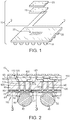
- FIG. 1 therein is shown an exploded pictorial view of an exemplary embodiment of a semiconductor chip device 10 that includes a semiconductor chip 15 mounted on a circuit board 20.
- the semiconductor chip 15 is adapted to have one or more other semiconductor chips, one of which is shown and labeled 25, mounted thereon in a stacked arrangement.
- the semiconductor chip 15 may interface electrically with the circuit board 20 by way of plural interconnect structures, which may be conductive pillars, solder joints or other types of interconnects.
- the semiconductor chip 15 may interface with the circuit board 20 by way of plural solder joints which may consist of respective solder structures (not visible) of the semiconductor chip 15 which join metallurgically to corresponding solder structures 30 of the circuit board 20.
- the circuit board 20 may in turn, interface electrically with another electronic device, such as another circuit board or other device by way of plural input/output structures.
- the input/output structures consist of an array of solder balls 35.
- interconnect structures such as pin grid arrays, land grid arrays or other interconnect structures could be used as well.
- the semiconductor chip 15 and the semiconductor chip 25 may be any of a myriad of different types of circuit devices used in electronics, such as, for example, microprocessors, graphics processors, combined microprocessor/graphics processors, application specific integrated circuits, memory devices, active optical devices, such as lasers, or the like, and may be single or multi-core or even stacked laterally with additional dice.
- the semiconductor chips 15 and 25 could be configured as an interposer with or without some logic circuits.
- the term "chip” includes an interposer.
- the semiconductor chips 15 and 25 may be constructed of bulk semiconductor, such as silicon or germanium, or semiconductor on insulator materials, such as silicon-on-insulator materials, or other chip materials.
- the circuit board 20 may be a semiconductor chip package substrate, a circuit card, or virtually any other type of printed circuit board. Although a monolithic structure could be used for the circuit board 20, a more typical configuration will utilize a buildup design.
- the circuit board 20 may consist of a central core upon which one or more buildup layers are formed and below which an additional one or more buildup layers are formed.
- the core itself may consist of a stack of one or more layers. If implemented as a semiconductor chip package substrate, the number of layers in the circuit board 20 can vary from four to sixteen or more, although less than four may be used. So-called "coreless" designs may be used as well.
- the layers of the circuit board 20 may consist of an insulating material, such as various well-known epoxies, interspersed with metal interconnects. A multi-layer configuration other than buildup could be used.
- the circuit board 20 may be composed of well-known ceramics or other materials suitable for package substrates or other printed circuit boards.
- the circuit board 20 is provided with a number of conductor traces and vias and other structures (not visible) in order to provide power, ground and signals transfers between the semiconductor chips 15 and 25 and another device, such as another circuit board for example.
- the circuit board 20 may be electrically connected to another device (not shown) by way of an input/output array such as the ball grid array depicted.
- the ball grid array includes the aforementioned plural solder balls 35 metallurgically bonded to respective ball pads (not shown).
- the ball pads (not shown) are interconnected to various conductor pads in the circuit board 20 by way of plural interconnect traces and vias and other structures that are not shown.
- the semiconductor chip 15 may include plural input/output structures that are designed to join metallurgically with the interconnect structures 30 of the circuit board 20.
- a couple of these exemplary interconnect structures may consist of respective solder bumps 40 and 45.
- the solder bumps 40 and 45 may be composed of various types of solders, such as lead-free or lead-based solders.
- solder-free solders examples include tin-silver (about 97.3% Sn 2.7% Ag), tin-copper (about 99% Sn 1% Cu), tin-silver-copper (about 96.5 % Sn 3% Ag 0.5% Cu) or the like.
- lead-based solders examples include tin-lead solders at or near eutectic proportions or the like.
- the solder balls 40 and 45 may be replaced with conductive pillars or other types of interconnect structures as desired.
- the solder bumps 40 and 45 are coupled to underbump metallization (UBM) structures 50 and 55, respectively.
- UBM underbump metallization
- the UBM structures 50 and 55 are formed on and in a passivation structure 60, which may be a monolithic or laminate film of insulating material.
- the UBM structures 50 and 55 are, in turn, connected to conductor structures or pads 65 and 70.
- the conductor pads 65 and 70 may consist of conductor pads that actually form part of what is a metallization layer 75 that includes plural alternating layers of interlevel dielectric and metallization layers (not shown). It should be understood that FIG. 2 is somewhat schematic in nature since the conductor pads 65 and 70 and the metallization layer 75 are not shown to scale.
- the interlevel dielectric layers (not shown) used for the metal interconnect layer 75 may consist of well-known silicon dioxide, other types of silicate glasses, low-K dielectric films or the like.
- the metallization structures in the layer 75 as well as the metal pads 65 and 70 and the UBM structures 50 and 55 may be composed of various conductors, such as copper, silver, nickel, platinum, gold, aluminum, palladium, alloys or laminates of these or the like.
- the conductor pads 65 and 70 may be formed by well-known material placement and patterning techniques, such as plating, chemical vapor deposition (CVD) or the like, and lithography with chemical etching laser ablation or the like.
- the semiconductor chip 15 is a multi-strata structure in that there may be a bulk stratum or layer 80, a device stratum or layer 85 in which large numbers of transistors, capacitors and other circuit devices may be formed, and a metallization stratum or layer 75.
- the metallization layer 75 may be formed as a series of metallization layers sandwiched between interlevel dielectric layers that are successively built up on the device layer 85. Because the semiconductor chip 15 is designed to have another semiconductor chip, such as the semiconductor chip 25, stacked thereon, a backside metallization scheme is provided. In this regard, a redistribution layer (RDL) 90 may be formed on the semiconductor layer 80.
- RDL redistribution layer
- the RDL 90 may be monolithic or a laminate structure of one or more layers of build-up or other wise deposited insulating material interwoven with one or more RDL metallization structures that may be on the same or different levels. In this illustrative embodiment, RDL metallization structures 95 and 100 are visible.
- the RDL 90 may be topped with an insulating or passivation layer 105 and plural input/output structures 110.
- the passivation layer 105 may be monolithic or a laminate of plural insulating films and may be composed of the same types of materials used for the passivation structure layer 60 described elsewhere herein.
- the input/output structures 110 may be conductive pillars, pads, solder joints or the like, and are used to establish electrical interfaces with the semiconductor chip 25 depicted in FIG. 2 .
- the interconnect structures 110 may be composed of various conductors, such as copper, silver, nickel, platinum, gold, aluminum, palladium, alloys or laminates of these, solders or the like.
- the RDL structures 95 and 100 may connect to one or more of the interconnect structures 110.
- plural TSVs may be formed in the semiconductor layer 80 to extend through the device layer 85 and the metallization layer 75 and join the RDL structure 95 to the conductor pad 65.
- respective ends 127 of the TSVs contact the conductor pad 65 and opposite ends 129 thereof contact the RDL structure 95.
- a similar plurality of TSVs 130, 135 and 140 may join the RDL structure 100 to the conductor pad 70 electrically.
- TSV semiconductor layer 80
- the embodiments disclosed herein utilize plural TSVs for a given conductor pad, such as the TSVs 115, 120 and 125 and the conductor pad 65.
- the use of multiple TSVs for a given conductor pad provides improved spread of thermal stresses and lowers current density and thus Joule heating, which can enhance electromigration lifespan.
- the failure of one of the TSVs due to, for example, a stress migration fracture can be compensated for by the other remaining TSVs.
- the TSVs 115, 120, 125, 130, 135 and 140 may be composed of a variety of materials, such as copper, tungsten, graphene, aluminum, platinum, gold, palladium, alloys of these or like. Clad structures are envisioned.
- FIG. 3 is a sectional view of FIG. 2 taken at section 3-3.
- section 3-3 passes through the TSVs 115, 120 and 125 near the conductor pad 65. Attention is now turned to FIG. 3 . Note that because of the location of section 3-3, the TSVs 115, 120 and 125 appear in section but the underlying conductor pad 65 is obscured by the metallization layer 75 and thus is shown in phantom.
- the TSVs connected to the conductor pad 65 may be more numerous than three TSVs 115, 120 and 125 and indeed here may include six more TSVs collectively labeled 145.
- the TSVs 115, 120, 125 and 145 may be arranged in an array that generally tracks the footprint of the underlying conductor pad 65.
- the skilled artisan will appreciate that the actual spatial arrangement of the TSVs connected to a given conductor pad may take on a variety of different shapes as can the conductor pad 65.
- the TSVs 115, 120, 125 and 145 may be generally monolithic in construction. However, and as described in conjunction with an alternate embodiment depicted in FIG. 4 , other arrangements may be used as well.
- FIG. 4 is a sectional view like FIG. 3 but of an alternate exemplary embodiment of plural TSVs 115' connected to an underlying conductor pad 65.
- the conductor pad 65 is again shown in phantom since it is actually positioned below the metallization layer 75.
- the TSVs 115' may consist of a jacket 150 and a polymer core 155.
- the jacket 150 may be composed of copper, tungsten, graphene, aluminum, platinum, gold, palladium, alloys of these or like.
- the polymer core 155 may be composed of a variety of polymers which may be conducting or non-conducting as desired. Examples include Namics 119, well-known epoxies or the like. These so-called annular TSVs can be formed by carefully tailored plating by way of tightly controlled electric field generation during a plating process.
- FIG. 5 is a sectional view like FIG. 3 , but of an alternate exemplary embodiment where multiple TSVs 115" are connected to the underlying conductor pad 65, which is again shown in phantom due to its position beneath the metallization layer 75.
- the TSVs 115" are arranged in a cross-like arrangement that does not necessarily match the somewhat rectangular footprint of the conductor pad 65.
- a great variety of arrangements may be used and still achieve the technical benefits of multiple TSVs tied to a given conductor pad.
- the various TSVs are fabricated as a continuous structure from top to bottom, that is, through the semiconductor device layer 85 and metallization layer 75 shown in FIG. 2 .
- FIG. 6 is a sectional view like FIG. 2 , but of an alternate exemplary embodiment of a semiconductor chip 15', which may be configured substantially like the semiconductor chip 15 described elsewhere herein with a few notable exceptions.
- plural TSVs 160, 162 and 164 may connect to the UBM structure 50 and plural TSVs 166, 168 and 169 may connect to the UBM structure 55.
- the TSVs 160 and 164 connect by way of respective TSV extensions 170 and 172 and the TSVs 166 and 169 connect by way of respective TSV extensions 174 and 176.
- the TSV extensions 170, 172, 174 and 176 may be formed through the passivation structure 60.
- FIG. 7 is a sectional view of the semiconductor chip 15 at a preliminary stage of processing.
- the device layer 85 has been fabricated using a multitude of well-known processing steps.
- the metallization layer 75 may also be fully or partially completed or not prior to TSV formation.
- the semiconductor chip 15 has a thickness Z, taken up primarily by the semiconductor layer 80, that is larger than the final thickness following the formation of the TSVs and the RDL 90 as shown in FIG. 2 .
- a suitable lithography mask 178 may be applied to the device layer 85 and patterned lithographically to establish openings 180, 184, 188, 192, 196 and 198, which correspond to the desired locations for the subsequently formed TSVs 115, 120, 125, 130, 135 and 140.
- the mask 178 may be composed of well-known photoresist materials of either positive or negative tone.
- a non-contact or even a hard mask could be used.
- a material removal process may be used to form deep trenches 200, 205, 210, 215, 220 and 225 in the semiconductor layer 80.
- the trenches 200, 205, 210, 215, 220 and 225 may be formed by chemical etching with or without plasma enhancement or other material removal techniques. It might be possible to use laser ablation although care should be exercised to avoid excessive thermal heating.
- the openings 180, 184, 188, 192, 196 and 198 in the mask 178 are patterned to have the desired footprint for the ultimately formed trenches 200, 205, 210, 215, 220 and 225.
- FIG. 9 shows a sectional view of the trench 200 shown at greater magnification.
- a liner layer 230 may be formed in the trench 200 and coat not only the sidewalls of the trench 200 but also the sidewalls of the device layer 85.
- the liner layer 230 may be composed of a variety of materials, such as silicon dioxide. Well-known CVD techniques with or without plasma enhancement may be used to deposit the liner layer 230.
- the same may be done with regard to the other trenches 205, 210, 215, 220 and 225.
- the mask 178 shown in FIG. 8 may be removed before or after formation of the liner layer 230 by ashing, solvent stripping or the like, or lift off if a non-contact mask is used.
- the TSVs 115, 120, 125, 130, 135 and 140 may be formed in the respective trenches 200, 205, 210, 215, 220 and 225 as shown in FIG. 10 .
- the TSVs 115, 120, 125, 130, 135 and 140 may be formed in the respective trenches 200, 205, 210, 215, 220 and 225 as full formed columns or as annular TSVs as desired.
- the plating process may be a single step biased plating process or may be an unbiased seed layer plating process followed by a biased plating process as desired.
- the semiconductor layer 80 may be thinned as shown in FIG. 11 .
- portions 227 of the semiconductor layer 80 may be removed advantageously by chemical mechanical planarization (CMP), although other material removal techniques could be used in lieu of or in conjunction with CMP.
- CMP chemical mechanical planarization
- the RDL 90 depicted in FIG. 2 may be fabricated using well-known insulating material deposition and conductor material deposition and patterning techniques that may number over multiple layers depending upon the complexity of the RDL 90.
- the fabrication of the passivation structure 95 and the interconnect structures 110 may follow the formation of the RDL 90.
- the semiconductor chip 25 may be stacked on the semiconductor chip 15 and electrically connected thereto by solder reflow, compression bonding or other techniques depending on the type of chip-to-chip interface used.
- the skilled artisan will appreciate that the semiconductor chip 25 could be stacked on the semiconductor chip 15 at the wafer level or die level as desired.
- the semiconductor chips 15 and 25, may be mounted to the circuit board 20, singly or en masse.
- any of the exemplary embodiments disclosed herein may be embodied in instructions disposed in a computer readable medium, such as, for example, semiconductor, magnetic disk, optical disk or other storage medium or as a computer data signal.
- the instructions or software may be capable of synthesizing and/or simulating the circuit structures disclosed herein.
- an electronic design automation program such as Cadence APD, Cadence Spectra, Encore or the like, may be used to synthesize the disclosed circuit structures.
- the resulting code may be used to fabricate the disclosed circuit structures.
Description
- This invention relates generally to semiconductor processing, and more particularly to semiconductor chips incorporating thru-silicon-vias and methods of fabricating the same.
- Some time ago semiconductor chip designers began stacking multiple semiconductor dice (aka "dies") vertically in order to obtain more functionality without an attendant increase in required package substrate or circuit board area. A variety of techniques have been used to electrically connect adjacent dice in such stacked arrangements. One technique has involved the use of wire bonds leading from contact pads on one die to corresponding contact pads on an adjacent die. Another technique that has been introduced more recently involves the use of so-called thru-silicon-vias (TSV). A typical TSV is a conductive via that extends nearly or perhaps entirely through a semiconductor chip, depending on the presence or absence of any intervening conductor pads at one or the other of the principal surfaces of the chip.
- A typical conventional TSV provides electrical routing between opposite principal surfaces of a semiconductor chip. On one side, the conventional TSV is connected to some type of input/output structure (I/O), which is often a solder bump designed to form a solder joint with a package substrate during flip-chip solder reflow. The TSV is not connected directly to the solder bump, but to some intervening structure, such as an outermost metallization structure like a bump pad. The other or backside end of the TSV is connected to some form of backside I/O structure, typically through some intermediary conductor structure. The conventional TSV arrangement includes a single TSV metallurgically joined to a single bump pad.
- Conventional TSVs are subjected to Joule heating and electromigration issues that vary in intensity depending on power levels, thermal management, die size and other factors. A one-to-one TSV to bump pad arrangement is subjected to such environmental considerations.
-
US 2006/202347 discloses a through electrode extending through a silicon substrate to establish electrical connection. -
US 2009/294983 discloses a conductive via of a semiconductor device. -
US 2010/032843 discloses a system and method for forming under bump metalisation layers. - The present invention is directed to overcoming or reducing the effects of one or more of the foregoing disadvantages.
- In accordance with one aspect of the present invention, a method of manufacturing is provided that includes forming a first plurality of conductive vias in a layer of a first semiconductor chip. The first plurality of conductive vias includes first ends and second ends. Conductive via extensions are formed on the first ends of some of the first conductive vias but not on one or more other of the first conductive vias. A first conductor pad is formed in ohmic contact with the conductive via extensions and the one or more other of the first conductive vias.
- In accordance with another aspect of the present invention, an apparatus is provided that includes a first semiconductor chip including a layer and a first conductor pad coupled to the first semiconductor chip. A first plurality of conductive vias traverses the layer and has first ends and second ends. The first ends of the one or more of the first plurality of conductive vias are in ohmic contact with the first conductor pad. A conductive via extension on each of the first ends of the others of the first plurality of conductive vias and in ohmic contact with the first conductor pad.
- The foregoing and other advantages of the invention will become apparent upon reading the following detailed description and upon reference to the drawings in which:
-
FIG. 1 is an exploded pictorial view of an exemplary embodiment of a semiconductor chip device that includes a semiconductor chip mounted on a circuit board; -
FIG. 2 is a sectional view ofFIG. 1 taken at section 2-2; and does not form part of the invention -
FIG. 3 is a sectional view ofFIG. 2 taken at section 3-3; and does not form part of the invention -
FIG. 4 is a sectional view likeFIG. 3 but of an alternate example of plural TSVs connected to an underlying conductor pad; which do not form part of the invention -
FIG. 5 is a sectional view likeFIG. 3 , but of an alternate example in which multiple TSVs are connected to an underlying conductor pad; and which do not form part of the invention -
FIG. 6 is a sectional view likeFIG. 2 , but of an exemplary embodiment of a semiconductor chip in which plural TSVs are multi-component; -
FIG. 7 is a sectional view of a semiconductor chip undergoing exemplary lithographic processing; -
FIG. 8 is a sectional view likeFIG. 7 , but depicting exemplary formation of TSV trenches; -
FIG. 9 shows a sectional view depicting a portion ofFIG. 8 at greater magnification; -
FIG. 10 is a sectional view likeFIG. 8 , but depicting exemplary TSV formation; -
FIG. 11 is a sectional view likeFIG. 10 depicting exemplary thinning of the semiconductor chip; -
FIG. 12 is a sectional view likeFIG. 11 depicting the semiconductor chip following thinning; and -
FIG. 13 is a sectional view likeFIG. 2 , but depicting an alternate exemplary semiconductor chip incorporating plural TSVs with conductive pillar input/outputs. - Various embodiments of a semiconductor chip device that includes two or more stacked substrates are described herein. One example includes at least one semiconductor chip with plural TSVs. However, plural TSVs are formed in ohmic contact with a given conductor structure, such as a bump or pillar pad. With redundancy in TSV-to-pad connections, failure of a given TSV need not open circuit the pad. Additional details will now be described.
- In the drawings described below, reference numerals are generally repeated where identical elements appear in more than one figure. Turning now to the drawings, and in particular to
FIG. 1 , therein is shown an exploded pictorial view of an exemplary embodiment of asemiconductor chip device 10 that includes asemiconductor chip 15 mounted on acircuit board 20. Thesemiconductor chip 15 is adapted to have one or more other semiconductor chips, one of which is shown and labeled 25, mounted thereon in a stacked arrangement. Thesemiconductor chip 15 may interface electrically with thecircuit board 20 by way of plural interconnect structures, which may be conductive pillars, solder joints or other types of interconnects. In this illustrative embodiment, thesemiconductor chip 15 may interface with thecircuit board 20 by way of plural solder joints which may consist of respective solder structures (not visible) of thesemiconductor chip 15 which join metallurgically tocorresponding solder structures 30 of thecircuit board 20. Thecircuit board 20, may in turn, interface electrically with another electronic device, such as another circuit board or other device by way of plural input/output structures. In this illustrative embodiment, the input/output structures consist of an array ofsolder balls 35. However, the skilled artisan will appreciate that other types of interconnect structures, such as pin grid arrays, land grid arrays or other interconnect structures could be used as well. - The exemplary structures of the
semiconductor chip 15 disclosed herein are not dependent on a particular electronic functionality. Thus, thesemiconductor chip 15 and thesemiconductor chip 25 may be any of a myriad of different types of circuit devices used in electronics, such as, for example, microprocessors, graphics processors, combined microprocessor/graphics processors, application specific integrated circuits, memory devices, active optical devices, such as lasers, or the like, and may be single or multi-core or even stacked laterally with additional dice. Furthermore, one or both of thesemiconductor chips semiconductor chips - The exemplary structures of the
semiconductor chip 15 disclosed herein are not dependent on a particular electronic circuit board functionality. Thus, thecircuit board 20 may be a semiconductor chip package substrate, a circuit card, or virtually any other type of printed circuit board. Although a monolithic structure could be used for thecircuit board 20, a more typical configuration will utilize a buildup design. In this regard, thecircuit board 20 may consist of a central core upon which one or more buildup layers are formed and below which an additional one or more buildup layers are formed. The core itself may consist of a stack of one or more layers. If implemented as a semiconductor chip package substrate, the number of layers in thecircuit board 20 can vary from four to sixteen or more, although less than four may be used. So-called "coreless" designs may be used as well. The layers of thecircuit board 20 may consist of an insulating material, such as various well-known epoxies, interspersed with metal interconnects. A multi-layer configuration other than buildup could be used. Optionally, thecircuit board 20 may be composed of well-known ceramics or other materials suitable for package substrates or other printed circuit boards. Thecircuit board 20 is provided with a number of conductor traces and vias and other structures (not visible) in order to provide power, ground and signals transfers between the semiconductor chips 15 and 25 and another device, such as another circuit board for example. Thecircuit board 20 may be electrically connected to another device (not shown) by way of an input/output array such as the ball grid array depicted. The ball grid array includes the aforementionedplural solder balls 35 metallurgically bonded to respective ball pads (not shown). The ball pads (not shown) are interconnected to various conductor pads in thecircuit board 20 by way of plural interconnect traces and vias and other structures that are not shown. - Additional details of the
semiconductor chip 15 will be described in conjunction withFIG. 2 , which is a sectional view ofFIG. 1 taken at section 2-2. Before turning to the discussion ofFIG. 2 , note that section 2-2 ofFIG. 1 passes through a small portion of thesemiconductor chip 15. With that backdrop, attention is now turned toFIG. 2 . As noted briefly above, thesemiconductor chip 15 may include plural input/output structures that are designed to join metallurgically with theinterconnect structures 30 of thecircuit board 20. A couple of these exemplary interconnect structures may consist of respective solder bumps 40 and 45. The solder bumps 40 and 45 may be composed of various types of solders, such as lead-free or lead-based solders. Examples of suitable lead-free solders include tin-silver (about 97.3% Sn 2.7% Ag), tin-copper (about 99% Sn 1% Cu), tin-silver-copper (about 96.5 % Sn 3% Ag 0.5% Cu) or the like. Examples of lead-based solders include tin-lead solders at or near eutectic proportions or the like. As noted above, thesolder balls structures UBM structures UBM structures pads conductor pads metallization layer 75 that includes plural alternating layers of interlevel dielectric and metallization layers (not shown). It should be understood thatFIG. 2 is somewhat schematic in nature since theconductor pads metallization layer 75 are not shown to scale. In any event, the interlevel dielectric layers (not shown) used for themetal interconnect layer 75 may consist of well-known silicon dioxide, other types of silicate glasses, low-K dielectric films or the like. The metallization structures in thelayer 75 as well as themetal pads UBM structures conductor pads - The
semiconductor chip 15 is a multi-strata structure in that there may be a bulk stratum orlayer 80, a device stratum orlayer 85 in which large numbers of transistors, capacitors and other circuit devices may be formed, and a metallization stratum orlayer 75. Themetallization layer 75 may be formed as a series of metallization layers sandwiched between interlevel dielectric layers that are successively built up on thedevice layer 85. Because thesemiconductor chip 15 is designed to have another semiconductor chip, such as thesemiconductor chip 25, stacked thereon, a backside metallization scheme is provided. In this regard, a redistribution layer (RDL) 90 may be formed on thesemiconductor layer 80. TheRDL 90 may be monolithic or a laminate structure of one or more layers of build-up or other wise deposited insulating material interwoven with one or more RDL metallization structures that may be on the same or different levels. In this illustrative embodiment,RDL metallization structures RDL 90 may be topped with an insulating orpassivation layer 105 and plural input/output structures 110. Thepassivation layer 105 may be monolithic or a laminate of plural insulating films and may be composed of the same types of materials used for the passivation structure layer 60 described elsewhere herein. The input/output structures 110 may be conductive pillars, pads, solder joints or the like, and are used to establish electrical interfaces with thesemiconductor chip 25 depicted inFIG. 2 . Theinterconnect structures 110 may be composed of various conductors, such as copper, silver, nickel, platinum, gold, aluminum, palladium, alloys or laminates of these, solders or the like. TheRDL structures interconnect structures 110. - To establish conducting pathways between
opposite sides semiconductor chip 15, and more particularly between theRDL structures conductor pads semiconductor layer 80 to extend through thedevice layer 85 and themetallization layer 75 and join theRDL structure 95 to theconductor pad 65. In this way, respective ends 127 of the TSVs contact theconductor pad 65 and opposite ends 129 thereof contact theRDL structure 95. A similar plurality ofTSVs RDL structure 100 to theconductor pad 70 electrically. It should be understood that the terms "TSV" and "semiconductor" are used generically herein, in that thesemiconductor layer 80 may be composed of material(s) other than silicon. Unlike a conventional semiconductor chip design utilizing a single TSV per pad, the embodiments disclosed herein utilize plural TSVs for a given conductor pad, such as theTSVs conductor pad 65. The use of multiple TSVs for a given conductor pad provides improved spread of thermal stresses and lowers current density and thus Joule heating, which can enhance electromigration lifespan. With multiple TSVs connected to a given conductor pad, the failure of one of the TSVs due to, for example, a stress migration fracture, can be compensated for by the other remaining TSVs. TheTSVs - Additional details of the
TSVs FIG. 3 , which is a sectional view ofFIG. 2 taken at section 3-3. Before turning to section 3-3 in earnest, it should be noted that section 3-3 passes through theTSVs conductor pad 65. Attention is now turned toFIG. 3 . Note that because of the location of section 3-3, theTSVs underlying conductor pad 65 is obscured by themetallization layer 75 and thus is shown in phantom. The TSVs connected to theconductor pad 65 may be more numerous than threeTSVs TSVs underlying conductor pad 65. However, the skilled artisan will appreciate that the actual spatial arrangement of the TSVs connected to a given conductor pad may take on a variety of different shapes as can theconductor pad 65. Note also that theTSVs FIG. 4 , other arrangements may be used as well. - Attention is now turned to
FIG. 4 , which is a sectional view likeFIG. 3 but of an alternate exemplary embodiment of plural TSVs 115' connected to anunderlying conductor pad 65. Here, theconductor pad 65 is again shown in phantom since it is actually positioned below themetallization layer 75. As just noted, other than a monolithic arrangement may be used for a given TSV. Thus, the TSVs 115' may consist of ajacket 150 and apolymer core 155. Thejacket 150 may be composed of copper, tungsten, graphene, aluminum, platinum, gold, palladium, alloys of these or like. Thepolymer core 155 may be composed of a variety of polymers which may be conducting or non-conducting as desired. Examples include Namics 119, well-known epoxies or the like. These so-called annular TSVs can be formed by carefully tailored plating by way of tightly controlled electric field generation during a plating process. - As noted above, the arrangement of TSVs tied to a given conductor pad may be subject to great variation. In this regard, attention is now turned to
FIG. 5 , which is a sectional view likeFIG. 3 , but of an alternate exemplary embodiment wheremultiple TSVs 115" are connected to theunderlying conductor pad 65, which is again shown in phantom due to its position beneath themetallization layer 75. Here, theTSVs 115" are arranged in a cross-like arrangement that does not necessarily match the somewhat rectangular footprint of theconductor pad 65. Again, a great variety of arrangements may be used and still achieve the technical benefits of multiple TSVs tied to a given conductor pad. - In the foregoing illustrative embodiments, the various TSVs are fabricated as a continuous structure from top to bottom, that is, through the
semiconductor device layer 85 andmetallization layer 75 shown inFIG. 2 . However, the skilled artisan will appreciate that multi-tiered structures could be used for TSVs. In this regard, attention is now turned toFIG. 6 , which is a sectional view likeFIG. 2 , but of an alternate exemplary embodiment of a semiconductor chip 15', which may be configured substantially like thesemiconductor chip 15 described elsewhere herein with a few notable exceptions. Here,plural TSVs UBM structure 50 andplural TSVs UBM structure 55. However, theTSVs respective TSV extensions TSVs respective TSV extensions TSV extensions - An exemplary process for forming the plural TSVs may be understood by referring now to
FIGS. 7, 8, 9 ,10, 11 and 12 and initially toFIG. 7 , which is a sectional view of thesemiconductor chip 15 at a preliminary stage of processing. At this stage, thedevice layer 85 has been fabricated using a multitude of well-known processing steps. Themetallization layer 75 may also be fully or partially completed or not prior to TSV formation. At this point, thesemiconductor chip 15 has a thickness Z, taken up primarily by thesemiconductor layer 80, that is larger than the final thickness following the formation of the TSVs and theRDL 90 as shown inFIG. 2 . At this point, asuitable lithography mask 178, may be applied to thedevice layer 85 and patterned lithographically to establishopenings TSVs mask 178 may be composed of well-known photoresist materials of either positive or negative tone. Optionally, a non-contact or even a hard mask could be used. - Referring now to
FIG. 8 , following the patterning of themask 178, a material removal process may be used to formdeep trenches semiconductor layer 80. Thetrenches openings mask 178 are patterned to have the desired footprint for the ultimately formedtrenches trenches semiconductor layer 80 as well as prevent migration of atoms, molecules or larger portions of the TSVs into thesemiconductor layer 80 and thedevice layer 85.FIG. 9 shows a sectional view of thetrench 200 shown at greater magnification. Aliner layer 230 may be formed in thetrench 200 and coat not only the sidewalls of thetrench 200 but also the sidewalls of thedevice layer 85. Theliner layer 230 may be composed of a variety of materials, such as silicon dioxide. Well-known CVD techniques with or without plasma enhancement may be used to deposit theliner layer 230. The same may be done with regard to theother trenches mask 178 shown inFIG. 8 may be removed before or after formation of theliner layer 230 by ashing, solvent stripping or the like, or lift off if a non-contact mask is used. - Following the removal of the
etch mask 178 shown inFIGS. 7 and 8 , theTSVs respective trenches FIG. 10 . As noted elsewhere herein, theTSVs respective trenches - To enable the
TSVs RDL 90 shown inFIG. 2 , thesemiconductor layer 80 may be thinned as shown inFIG. 11 . Here,portions 227 of thesemiconductor layer 80 may be removed advantageously by chemical mechanical planarization (CMP), although other material removal techniques could be used in lieu of or in conjunction with CMP. With theTSVs FIG. 12 , theRDL 90 depicted inFIG. 2 may be fabricated using well-known insulating material deposition and conductor material deposition and patterning techniques that may number over multiple layers depending upon the complexity of theRDL 90. Similarly, the fabrication of thepassivation structure 95 and theinterconnect structures 110 may follow the formation of theRDL 90. - Referring again to
FIG. 1 , thesemiconductor chip 25 may be stacked on thesemiconductor chip 15 and electrically connected thereto by solder reflow, compression bonding or other techniques depending on the type of chip-to-chip interface used. The skilled artisan will appreciate that thesemiconductor chip 25 could be stacked on thesemiconductor chip 15 at the wafer level or die level as desired. The semiconductor chips 15 and 25, may be mounted to thecircuit board 20, singly or en masse. - Any of the exemplary embodiments disclosed herein may be embodied in instructions disposed in a computer readable medium, such as, for example, semiconductor, magnetic disk, optical disk or other storage medium or as a computer data signal. The instructions or software may be capable of synthesizing and/or simulating the circuit structures disclosed herein. In an exemplary embodiment, an electronic design automation program, such as Cadence APD, Cadence Spectra, Encore or the like, may be used to synthesize the disclosed circuit structures. The resulting code may be used to fabricate the disclosed circuit structures.
- While the invention may be susceptible to various modifications and alternative forms, specific embodiments have been shown by way of example in the drawings and have been described in detail herein. However, it should be understood that the invention is not intended to be limited to the particular forms disclosed and the scope of protection is only defined by the appended claims.
Claims (14)
- A method of manufacturing, comprising:forming a first plurality of conductive vias (115, 120, 125, 160, 162, 164, 166, 168, 169) in a layer (80) of a first semiconductor chip (15, 151), the first plurality of conductive vias including first ends (127) and second ends (129);forming conductive via extensions (170, 172, 174, 176) on the first ends (127) of some of the first conductive vias (160, 164, 166, 169) but not on one or more other of the first conductive vias (162,168); andforming a first conductor pad (50, 55) in ohmic contact with the conductive via extensions (170, 172, 174, 176) and the one or more other of the first conductive vias (162, 168).
- The method of claim 1, comprising forming a conductor structure (95) in ohmic contact with the second ends of the first plurality of conductive vias.
- The method of claim 1, comprising mounting the first semiconductor chip on a circuit board (20).
- The method of claim 1, wherein the first plurality of conductive vias are formed by forming trenches (200, 205, 210) in the first semiconductor chip and placing conductor material in the trenches.
- A method of manufacturing, as claimed in claim 1,
the first semiconductor chip having a first side (112) and a second and opposite side (113);
wherein said first conductor pad (55, 60) is formed proximate the first side;
further comprising;
forming a second conductor pad (90) proximate the second side and in ohmic contact with the second ends of the first plurality of conductive vias. - The method of claim 1 or claim 5, comprising coupling an input/output structure (40) to the first conductor pad.
- The method of claim 6, wherein the input/output structure comprises a solder bump (40) or a conductive pillar (240).
- The method of claim 1 or claim 5, comprising stacking a second semiconductor chip (25) on the first semiconductor chip.
- The method of claim 1 or claim 5 wherein the first plurality of conductive vias include a polymer core and a conductor jacket around the polymer core.
- An apparatus, comprising:a first semiconductor chip (15) including a layer (80);a first conductor pad (55, 60) coupled to the first semiconductor chip;a first plurality of conductive vias (115, 120, 125, 160, 162, 164, 166, 168, 169) traversing the layer and having first ends (127) and second ends (129), the first ends of one or more of the first plurality of conductive vias (162, 168) in ohmic contact with the first conductor pad; anda conductive via extension (170, 172, 174, 176) on each of the first ends of others of the first plurality of conductive vias (162, 168) and in ohmic contact with the first conductor pad.
- The apparatus of claim 10, comprising a conductor structure (95) in ohmic contact with the second ends of the first plurality of conductive vias.
- The apparatus of claim 10, comprising a solder bump (40) or a conductive pillar (240) coupled to the first conductor pad.
- The apparatus of claim 10, comprising a second semiconductor chip (25) stacked on the first semiconductor chip.
- The apparatus of claim 10, comprising a circuit board (20) coupled to the first semiconductor chip.
Applications Claiming Priority (2)
| Application Number | Priority Date | Filing Date | Title |
|---|---|---|---|
| US12/878,542 US9437561B2 (en) | 2010-09-09 | 2010-09-09 | Semiconductor chip with redundant thru-silicon-vias |
| PCT/US2011/051027 WO2012034034A1 (en) | 2010-09-09 | 2011-09-09 | Semiconductor chip with redundant thru-silicon-vias |
Publications (2)
| Publication Number | Publication Date |
|---|---|
| EP2614523A1 EP2614523A1 (en) | 2013-07-17 |
| EP2614523B1 true EP2614523B1 (en) | 2020-11-25 |
Family
ID=44653600
Family Applications (1)
| Application Number | Title | Priority Date | Filing Date |
|---|---|---|---|
| EP11758061.3A Active EP2614523B1 (en) | 2010-09-09 | 2011-09-09 | Semiconductor chip with redundant thru-silicon-vias |
Country Status (5)
| Country | Link |
|---|---|
| US (3) | US9437561B2 (en) |
| EP (1) | EP2614523B1 (en) |
| JP (1) | JP6013336B2 (en) |
| KR (1) | KR101850121B1 (en) |
| WO (1) | WO2012034034A1 (en) |
Families Citing this family (25)
| Publication number | Priority date | Publication date | Assignee | Title |
|---|---|---|---|---|
| JP5826532B2 (en) * | 2010-07-15 | 2015-12-02 | 新光電気工業株式会社 | Semiconductor device and manufacturing method thereof |
| US8314498B2 (en) * | 2010-09-10 | 2012-11-20 | Aptina Imaging Corporation | Isolated bond pad with conductive via interconnect |
| JPWO2013057886A1 (en) * | 2011-10-17 | 2015-04-02 | パナソニックIpマネジメント株式会社 | Integrated circuit, multi-core processor device, and integrated circuit manufacturing method |
| US9030010B2 (en) * | 2012-09-20 | 2015-05-12 | Taiwan Semiconductor Manufacturing Company, Ltd. | Packaging devices and methods |
| US8866287B2 (en) | 2012-09-29 | 2014-10-21 | Intel Corporation | Embedded structures for package-on-package architecture |
| CN104037149A (en) * | 2013-03-05 | 2014-09-10 | 飞思卡尔半导体公司 | Lead frame and substrate semiconductor package |
| DE112013002916T5 (en) * | 2013-06-27 | 2015-03-05 | Intel IP Corporation | High conductivity, high frequency via for electronic equipment |
| JP2015041691A (en) * | 2013-08-21 | 2015-03-02 | 株式会社東芝 | Semiconductor device and semiconductor device manufacturing method |
| US9389972B2 (en) | 2014-05-13 | 2016-07-12 | International Business Machines Corporation | Data retrieval from stacked computer memory |
| US9405468B2 (en) | 2014-05-13 | 2016-08-02 | Globalfoundries Inc. | Stacked memory device control |
| KR101640076B1 (en) * | 2014-11-05 | 2016-07-15 | 앰코 테크놀로지 코리아 주식회사 | Stacked chip package and method for manufacturing the same |
| US9515017B2 (en) * | 2014-12-18 | 2016-12-06 | Intel Corporation | Ground via clustering for crosstalk mitigation |
| US9515035B2 (en) | 2014-12-19 | 2016-12-06 | International Business Machines Corporation | Three-dimensional integrated circuit integration |
| CN105990282B (en) * | 2015-02-27 | 2019-03-01 | 华为技术有限公司 | A kind of pinboard and electronic building brick |
| US10068181B1 (en) | 2015-04-27 | 2018-09-04 | Rigetti & Co, Inc. | Microwave integrated quantum circuits with cap wafer and methods for making the same |
| US10090251B2 (en) | 2015-07-24 | 2018-10-02 | Infineon Technologies Ag | Semiconductor chip having a dense arrangement of contact terminals |
| US10236245B2 (en) * | 2016-03-23 | 2019-03-19 | Dyi-chung Hu | Package substrate with embedded circuit |
| US11652067B2 (en) | 2016-12-28 | 2023-05-16 | Intel Corporation | Methods of forming substrate interconnect structures for enhanced thin seed conduction |
| US11121301B1 (en) | 2017-06-19 | 2021-09-14 | Rigetti & Co, Inc. | Microwave integrated quantum circuits with cap wafers and their methods of manufacture |
| US11276727B1 (en) | 2017-06-19 | 2022-03-15 | Rigetti & Co, Llc | Superconducting vias for routing electrical signals through substrates and their methods of manufacture |
| KR102019355B1 (en) * | 2017-11-01 | 2019-09-09 | 삼성전자주식회사 | Semiconductor package |
| KR102498883B1 (en) | 2018-01-31 | 2023-02-13 | 삼성전자주식회사 | Semiconductor device including through electrodes distributing current |
| TWI705547B (en) * | 2019-03-12 | 2020-09-21 | 力成科技股份有限公司 | Chip package structure and manufacturing method thereof |
| US11515173B2 (en) * | 2019-12-27 | 2022-11-29 | Taiwan Semiconductor Manufacturing Company, Ltd. | Semiconductor devices and methods of manufacturing |
| US11955417B2 (en) | 2021-12-14 | 2024-04-09 | Industrial Technology Research Institute | Electronic device having substrate with electrically floating vias |
Family Cites Families (20)
| Publication number | Priority date | Publication date | Assignee | Title |
|---|---|---|---|---|
| JPS6124240A (en) | 1984-07-13 | 1986-02-01 | Toshiba Corp | Semiconductor substrate |
| US6355950B1 (en) * | 1998-09-23 | 2002-03-12 | Intel Corporation | Substrate interconnect for power distribution on integrated circuits |
| US6352923B1 (en) * | 1999-03-01 | 2002-03-05 | United Microelectronics Corp. | Method of fabricating direct contact through hole type |
| JP4123682B2 (en) * | 2000-05-16 | 2008-07-23 | セイコーエプソン株式会社 | Semiconductor device and manufacturing method thereof |
| US7345350B2 (en) * | 2003-09-23 | 2008-03-18 | Micron Technology, Inc. | Process and integration scheme for fabricating conductive components, through-vias and semiconductor components including conductive through-wafer vias |
| JP4426482B2 (en) * | 2005-02-28 | 2010-03-03 | Okiセミコンダクタ株式会社 | Package base, method for manufacturing the same, and semiconductor package including the package base |
| US20070032059A1 (en) * | 2005-08-02 | 2007-02-08 | Harry Hedler | Method of manufacturing a semiconductor structure having a wafer through-contact and a corresponding semiconductor structure |
| US20070045844A1 (en) * | 2005-08-24 | 2007-03-01 | Andry Paul S | Alpha particle shields in chip packaging |
| JP4847072B2 (en) | 2005-08-26 | 2011-12-28 | 本田技研工業株式会社 | Semiconductor integrated circuit device and manufacturing method thereof |
| JP4415984B2 (en) | 2006-12-06 | 2010-02-17 | ソニー株式会社 | Manufacturing method of semiconductor device |
| JP2008244187A (en) * | 2007-03-28 | 2008-10-09 | Elpida Memory Inc | Through electrode and semiconductor device |
| JP4534096B2 (en) | 2007-04-12 | 2010-09-01 | ローム株式会社 | Semiconductor chip, manufacturing method thereof, and semiconductor device |
| US8134235B2 (en) * | 2007-04-23 | 2012-03-13 | Taiwan Semiconductor Manufacturing Co., Ltd. | Three-dimensional semiconductor device |
| KR101052870B1 (en) * | 2008-04-21 | 2011-07-29 | 주식회사 하이닉스반도체 | A laminated semiconductor package having a through electrode, a circuit board having the same, a semiconductor package having the same, and a semiconductor package |
| JP2009295616A (en) | 2008-06-02 | 2009-12-17 | Philtech Inc | Silicon substrate, method for manufacturing device, device and testing method |
| US7939449B2 (en) * | 2008-06-03 | 2011-05-10 | Micron Technology, Inc. | Methods of forming hybrid conductive vias including small dimension active surface ends and larger dimension back side ends |
| US8288872B2 (en) | 2008-08-05 | 2012-10-16 | Taiwan Semiconductor Manufacturing Company, Ltd. | Through silicon via layout |
| JP2010135348A (en) | 2008-12-02 | 2010-06-17 | Panasonic Corp | Method for forming through electrode |
| US8232137B2 (en) * | 2009-12-10 | 2012-07-31 | Intersil Americas Inc. | Heat conduction for chip stacks and 3-D circuits |
| US20110193212A1 (en) * | 2010-02-08 | 2011-08-11 | Qualcomm Incorporated | Systems and Methods Providing Arrangements of Vias |
-
2010
- 2010-09-09 US US12/878,542 patent/US9437561B2/en active Active
-
2011
- 2011-09-09 KR KR1020137007011A patent/KR101850121B1/en active IP Right Grant
- 2011-09-09 EP EP11758061.3A patent/EP2614523B1/en active Active
- 2011-09-09 WO PCT/US2011/051027 patent/WO2012034034A1/en active Application Filing
- 2011-09-09 JP JP2013528332A patent/JP6013336B2/en active Active
-
2016
- 2016-08-25 US US15/247,259 patent/US11469212B2/en active Active
-
2022
- 2022-10-11 US US17/963,729 patent/US20230031099A1/en active Pending
Non-Patent Citations (1)
| Title |
|---|
| None * |
Also Published As
| Publication number | Publication date |
|---|---|
| KR101850121B1 (en) | 2018-04-19 |
| JP6013336B2 (en) | 2016-10-25 |
| EP2614523A1 (en) | 2013-07-17 |
| US20120061821A1 (en) | 2012-03-15 |
| US11469212B2 (en) | 2022-10-11 |
| US9437561B2 (en) | 2016-09-06 |
| JP2013538460A (en) | 2013-10-10 |
| US20230031099A1 (en) | 2023-02-02 |
| WO2012034034A1 (en) | 2012-03-15 |
| CN103098204A (en) | 2013-05-08 |
| US20160365335A1 (en) | 2016-12-15 |
| KR20130097766A (en) | 2013-09-03 |
Similar Documents
| Publication | Publication Date | Title |
|---|---|---|
| US20230031099A1 (en) | Semiconductor chip with redundant thru-silicon-vias | |
| US8338961B2 (en) | Semiconductor chip with reinforcing through-silicon-vias | |
| TWI727463B (en) | Package and methods of forming the same | |
| JP2013538460A5 (en) | ||
| KR100772604B1 (en) | Integrated Electronic Chip and Interconnect Device and Process for Making the Same | |
| US6962867B2 (en) | Methods of fabrication of semiconductor dice having back side redistribution layer accessed using through-silicon vias and assemblies thereof | |
| US8691691B2 (en) | TSV pillar as an interconnecting structure | |
| WO2012177450A1 (en) | Semiconductor chip with dual polymer film interconnect structures | |
| KR20220085756A (en) | Semiconductor devices and methods of manufacture | |
| TWI735353B (en) | Integrated circuit package and manufacturing method thereof | |
| US20130256895A1 (en) | Stacked semiconductor components with universal interconnect footprint | |
| CN220895506U (en) | Semiconductor package | |
| US20220130781A1 (en) | Circuit substrate structure and manufacturing method thereof | |
| CN103098204B (en) | There is the semiconductor chip of redundancy silicon through hole |
Legal Events
| Date | Code | Title | Description |
|---|---|---|---|
| PUAI | Public reference made under article 153(3) epc to a published international application that has entered the european phase |
Free format text: ORIGINAL CODE: 0009012 |
|
| 17P | Request for examination filed |
Effective date: 20130327 |
|
| AK | Designated contracting states |
Kind code of ref document: A1 Designated state(s): AL AT BE BG CH CY CZ DE DK EE ES FI FR GB GR HR HU IE IS IT LI LT LU LV MC MK MT NL NO PL PT RO RS SE SI SK SM TR |
|
| DAX | Request for extension of the european patent (deleted) | ||
| RAP1 | Party data changed (applicant data changed or rights of an application transferred) |
Owner name: ATI TECHNOLOGIES ULC Owner name: ADVANCED MICRO DEVICES, INC. |
|
| RAP1 | Party data changed (applicant data changed or rights of an application transferred) |
Owner name: ATI TECHNOLOGIES ULC Owner name: ADVANCED MICRO DEVICES, INC. |
|
| STAA | Information on the status of an ep patent application or granted ep patent |
Free format text: STATUS: EXAMINATION IS IN PROGRESS |
|
| 17Q | First examination report despatched |
Effective date: 20191002 |
|
| GRAP | Despatch of communication of intention to grant a patent |
Free format text: ORIGINAL CODE: EPIDOSNIGR1 |
|
| STAA | Information on the status of an ep patent application or granted ep patent |
Free format text: STATUS: GRANT OF PATENT IS INTENDED |
|
| INTG | Intention to grant announced |
Effective date: 20200721 |
|
| GRAS | Grant fee paid |
Free format text: ORIGINAL CODE: EPIDOSNIGR3 |
|
| GRAA | (expected) grant |
Free format text: ORIGINAL CODE: 0009210 |
|
| STAA | Information on the status of an ep patent application or granted ep patent |
Free format text: STATUS: THE PATENT HAS BEEN GRANTED |
|
| AK | Designated contracting states |
Kind code of ref document: B1 Designated state(s): AL AT BE BG CH CY CZ DE DK EE ES FI FR GB GR HR HU IE IS IT LI LT LU LV MC MK MT NL NO PL PT RO RS SE SI SK SM TR |
|
| REG | Reference to a national code |
Ref country code: GB Ref legal event code: FG4D |
|
| REG | Reference to a national code |
Ref country code: CH Ref legal event code: EP |
|
| REG | Reference to a national code |
Ref country code: AT Ref legal event code: REF Ref document number: 1339265 Country of ref document: AT Kind code of ref document: T Effective date: 20201215 |
|
| REG | Reference to a national code |
Ref country code: DE Ref legal event code: R096 Ref document number: 602011069420 Country of ref document: DE |
|
| REG | Reference to a national code |
Ref country code: IE Ref legal event code: FG4D |
|
| REG | Reference to a national code |
Ref country code: AT Ref legal event code: MK05 Ref document number: 1339265 Country of ref document: AT Kind code of ref document: T Effective date: 20201125 |
|
| REG | Reference to a national code |
Ref country code: NL Ref legal event code: MP Effective date: 20201125 |
|
| PG25 | Lapsed in a contracting state [announced via postgrant information from national office to epo] |
Ref country code: NO Free format text: LAPSE BECAUSE OF FAILURE TO SUBMIT A TRANSLATION OF THE DESCRIPTION OR TO PAY THE FEE WITHIN THE PRESCRIBED TIME-LIMIT Effective date: 20210225 Ref country code: PT Free format text: LAPSE BECAUSE OF FAILURE TO SUBMIT A TRANSLATION OF THE DESCRIPTION OR TO PAY THE FEE WITHIN THE PRESCRIBED TIME-LIMIT Effective date: 20210325 Ref country code: FI Free format text: LAPSE BECAUSE OF FAILURE TO SUBMIT A TRANSLATION OF THE DESCRIPTION OR TO PAY THE FEE WITHIN THE PRESCRIBED TIME-LIMIT Effective date: 20201125 Ref country code: RS Free format text: LAPSE BECAUSE OF FAILURE TO SUBMIT A TRANSLATION OF THE DESCRIPTION OR TO PAY THE FEE WITHIN THE PRESCRIBED TIME-LIMIT Effective date: 20201125 Ref country code: GR Free format text: LAPSE BECAUSE OF FAILURE TO SUBMIT A TRANSLATION OF THE DESCRIPTION OR TO PAY THE FEE WITHIN THE PRESCRIBED TIME-LIMIT Effective date: 20210226 |
|
| PG25 | Lapsed in a contracting state [announced via postgrant information from national office to epo] |
Ref country code: PL Free format text: LAPSE BECAUSE OF FAILURE TO SUBMIT A TRANSLATION OF THE DESCRIPTION OR TO PAY THE FEE WITHIN THE PRESCRIBED TIME-LIMIT Effective date: 20201125 Ref country code: SE Free format text: LAPSE BECAUSE OF FAILURE TO SUBMIT A TRANSLATION OF THE DESCRIPTION OR TO PAY THE FEE WITHIN THE PRESCRIBED TIME-LIMIT Effective date: 20201125 Ref country code: LV Free format text: LAPSE BECAUSE OF FAILURE TO SUBMIT A TRANSLATION OF THE DESCRIPTION OR TO PAY THE FEE WITHIN THE PRESCRIBED TIME-LIMIT Effective date: 20201125 Ref country code: BG Free format text: LAPSE BECAUSE OF FAILURE TO SUBMIT A TRANSLATION OF THE DESCRIPTION OR TO PAY THE FEE WITHIN THE PRESCRIBED TIME-LIMIT Effective date: 20210225 Ref country code: AT Free format text: LAPSE BECAUSE OF FAILURE TO SUBMIT A TRANSLATION OF THE DESCRIPTION OR TO PAY THE FEE WITHIN THE PRESCRIBED TIME-LIMIT Effective date: 20201125 Ref country code: IS Free format text: LAPSE BECAUSE OF FAILURE TO SUBMIT A TRANSLATION OF THE DESCRIPTION OR TO PAY THE FEE WITHIN THE PRESCRIBED TIME-LIMIT Effective date: 20210325 |
|
| REG | Reference to a national code |
Ref country code: LT Ref legal event code: MG9D |
|
| PG25 | Lapsed in a contracting state [announced via postgrant information from national office to epo] |
Ref country code: HR Free format text: LAPSE BECAUSE OF FAILURE TO SUBMIT A TRANSLATION OF THE DESCRIPTION OR TO PAY THE FEE WITHIN THE PRESCRIBED TIME-LIMIT Effective date: 20201125 |
|
| PG25 | Lapsed in a contracting state [announced via postgrant information from national office to epo] |
Ref country code: SK Free format text: LAPSE BECAUSE OF FAILURE TO SUBMIT A TRANSLATION OF THE DESCRIPTION OR TO PAY THE FEE WITHIN THE PRESCRIBED TIME-LIMIT Effective date: 20201125 Ref country code: RO Free format text: LAPSE BECAUSE OF FAILURE TO SUBMIT A TRANSLATION OF THE DESCRIPTION OR TO PAY THE FEE WITHIN THE PRESCRIBED TIME-LIMIT Effective date: 20201125 Ref country code: LT Free format text: LAPSE BECAUSE OF FAILURE TO SUBMIT A TRANSLATION OF THE DESCRIPTION OR TO PAY THE FEE WITHIN THE PRESCRIBED TIME-LIMIT Effective date: 20201125 Ref country code: EE Free format text: LAPSE BECAUSE OF FAILURE TO SUBMIT A TRANSLATION OF THE DESCRIPTION OR TO PAY THE FEE WITHIN THE PRESCRIBED TIME-LIMIT Effective date: 20201125 Ref country code: CZ Free format text: LAPSE BECAUSE OF FAILURE TO SUBMIT A TRANSLATION OF THE DESCRIPTION OR TO PAY THE FEE WITHIN THE PRESCRIBED TIME-LIMIT Effective date: 20201125 Ref country code: SM Free format text: LAPSE BECAUSE OF FAILURE TO SUBMIT A TRANSLATION OF THE DESCRIPTION OR TO PAY THE FEE WITHIN THE PRESCRIBED TIME-LIMIT Effective date: 20201125 |
|
| REG | Reference to a national code |
Ref country code: DE Ref legal event code: R097 Ref document number: 602011069420 Country of ref document: DE |
|
| PG25 | Lapsed in a contracting state [announced via postgrant information from national office to epo] |
Ref country code: DK Free format text: LAPSE BECAUSE OF FAILURE TO SUBMIT A TRANSLATION OF THE DESCRIPTION OR TO PAY THE FEE WITHIN THE PRESCRIBED TIME-LIMIT Effective date: 20201125 |
|
| PLBE | No opposition filed within time limit |
Free format text: ORIGINAL CODE: 0009261 |
|
| STAA | Information on the status of an ep patent application or granted ep patent |
Free format text: STATUS: NO OPPOSITION FILED WITHIN TIME LIMIT |
|
| PG25 | Lapsed in a contracting state [announced via postgrant information from national office to epo] |
Ref country code: IT Free format text: LAPSE BECAUSE OF FAILURE TO SUBMIT A TRANSLATION OF THE DESCRIPTION OR TO PAY THE FEE WITHIN THE PRESCRIBED TIME-LIMIT Effective date: 20201125 Ref country code: AL Free format text: LAPSE BECAUSE OF FAILURE TO SUBMIT A TRANSLATION OF THE DESCRIPTION OR TO PAY THE FEE WITHIN THE PRESCRIBED TIME-LIMIT Effective date: 20201125 Ref country code: NL Free format text: LAPSE BECAUSE OF FAILURE TO SUBMIT A TRANSLATION OF THE DESCRIPTION OR TO PAY THE FEE WITHIN THE PRESCRIBED TIME-LIMIT Effective date: 20201125 |
|
| 26N | No opposition filed |
Effective date: 20210826 |
|
| PG25 | Lapsed in a contracting state [announced via postgrant information from national office to epo] |
Ref country code: ES Free format text: LAPSE BECAUSE OF FAILURE TO SUBMIT A TRANSLATION OF THE DESCRIPTION OR TO PAY THE FEE WITHIN THE PRESCRIBED TIME-LIMIT Effective date: 20201125 Ref country code: SI Free format text: LAPSE BECAUSE OF FAILURE TO SUBMIT A TRANSLATION OF THE DESCRIPTION OR TO PAY THE FEE WITHIN THE PRESCRIBED TIME-LIMIT Effective date: 20201125 |
|
| REG | Reference to a national code |
Ref country code: CH Ref legal event code: PL |
|
| REG | Reference to a national code |
Ref country code: BE Ref legal event code: MM Effective date: 20210930 |
|
| PG25 | Lapsed in a contracting state [announced via postgrant information from national office to epo] |
Ref country code: IS Free format text: LAPSE BECAUSE OF FAILURE TO SUBMIT A TRANSLATION OF THE DESCRIPTION OR TO PAY THE FEE WITHIN THE PRESCRIBED TIME-LIMIT Effective date: 20210325 Ref country code: MC Free format text: LAPSE BECAUSE OF FAILURE TO SUBMIT A TRANSLATION OF THE DESCRIPTION OR TO PAY THE FEE WITHIN THE PRESCRIBED TIME-LIMIT Effective date: 20201125 |
|
| PG25 | Lapsed in a contracting state [announced via postgrant information from national office to epo] |
Ref country code: LU Free format text: LAPSE BECAUSE OF NON-PAYMENT OF DUE FEES Effective date: 20210909 Ref country code: IE Free format text: LAPSE BECAUSE OF NON-PAYMENT OF DUE FEES Effective date: 20210909 Ref country code: FR Free format text: LAPSE BECAUSE OF NON-PAYMENT OF DUE FEES Effective date: 20210930 Ref country code: BE Free format text: LAPSE BECAUSE OF NON-PAYMENT OF DUE FEES Effective date: 20210930 |
|
| PG25 | Lapsed in a contracting state [announced via postgrant information from national office to epo] |
Ref country code: LI Free format text: LAPSE BECAUSE OF NON-PAYMENT OF DUE FEES Effective date: 20210930 Ref country code: CH Free format text: LAPSE BECAUSE OF NON-PAYMENT OF DUE FEES Effective date: 20210930 |
|
| PG25 | Lapsed in a contracting state [announced via postgrant information from national office to epo] |
Ref country code: HU Free format text: LAPSE BECAUSE OF FAILURE TO SUBMIT A TRANSLATION OF THE DESCRIPTION OR TO PAY THE FEE WITHIN THE PRESCRIBED TIME-LIMIT; INVALID AB INITIO Effective date: 20110909 Ref country code: CY Free format text: LAPSE BECAUSE OF FAILURE TO SUBMIT A TRANSLATION OF THE DESCRIPTION OR TO PAY THE FEE WITHIN THE PRESCRIBED TIME-LIMIT Effective date: 20201125 |
|
| P01 | Opt-out of the competence of the unified patent court (upc) registered |
Effective date: 20230530 |
|
| PGFP | Annual fee paid to national office [announced via postgrant information from national office to epo] |
Ref country code: GB Payment date: 20230912 Year of fee payment: 13 |
|
| PGFP | Annual fee paid to national office [announced via postgrant information from national office to epo] |
Ref country code: DE Payment date: 20230926 Year of fee payment: 13 |