EP2613439A1 - Acoustic wave device - Google Patents
Acoustic wave device Download PDFInfo
- Publication number
- EP2613439A1 EP2613439A1 EP11821372.7A EP11821372A EP2613439A1 EP 2613439 A1 EP2613439 A1 EP 2613439A1 EP 11821372 A EP11821372 A EP 11821372A EP 2613439 A1 EP2613439 A1 EP 2613439A1
- Authority
- EP
- European Patent Office
- Prior art keywords
- silicon oxide
- oxide film
- doped
- molecule
- acoustic wave
- Prior art date
- Legal status (The legal status is an assumption and is not a legal conclusion. Google has not performed a legal analysis and makes no representation as to the accuracy of the status listed.)
- Granted
Links
Images





Classifications
-
- H—ELECTRICITY
- H10—SEMICONDUCTOR DEVICES; ELECTRIC SOLID-STATE DEVICES NOT OTHERWISE PROVIDED FOR
- H10N—ELECTRIC SOLID-STATE DEVICES NOT OTHERWISE PROVIDED FOR
- H10N30/00—Piezoelectric or electrostrictive devices
- H10N30/80—Constructional details
- H10N30/87—Electrodes or interconnections, e.g. leads or terminals
-
- H—ELECTRICITY
- H03—ELECTRONIC CIRCUITRY
- H03H—IMPEDANCE NETWORKS, e.g. RESONANT CIRCUITS; RESONATORS
- H03H9/00—Networks comprising electromechanical or electro-acoustic elements; Electromechanical resonators
- H03H9/02—Details
- H03H9/02535—Details of surface acoustic wave devices
- H03H9/02818—Means for compensation or elimination of undesirable effects
- H03H9/02834—Means for compensation or elimination of undesirable effects of temperature influence
-
- H—ELECTRICITY
- H03—ELECTRONIC CIRCUITRY
- H03H—IMPEDANCE NETWORKS, e.g. RESONANT CIRCUITS; RESONATORS
- H03H9/00—Networks comprising electromechanical or electro-acoustic elements; Electromechanical resonators
- H03H9/02—Details
- H03H9/02007—Details of bulk acoustic wave devices
- H03H9/02086—Means for compensation or elimination of undesirable effects
- H03H9/02102—Means for compensation or elimination of undesirable effects of temperature influence
-
- H—ELECTRICITY
- H03—ELECTRONIC CIRCUITRY
- H03H—IMPEDANCE NETWORKS, e.g. RESONANT CIRCUITS; RESONATORS
- H03H9/00—Networks comprising electromechanical or electro-acoustic elements; Electromechanical resonators
- H03H9/02—Details
- H03H9/125—Driving means, e.g. electrodes, coils
- H03H9/13—Driving means, e.g. electrodes, coils for networks consisting of piezoelectric or electrostrictive materials
- H03H9/131—Driving means, e.g. electrodes, coils for networks consisting of piezoelectric or electrostrictive materials consisting of a multilayered structure
-
- H—ELECTRICITY
- H03—ELECTRONIC CIRCUITRY
- H03H—IMPEDANCE NETWORKS, e.g. RESONANT CIRCUITS; RESONATORS
- H03H9/00—Networks comprising electromechanical or electro-acoustic elements; Electromechanical resonators
- H03H9/15—Constructional features of resonators consisting of piezoelectric or electrostrictive material
- H03H9/17—Constructional features of resonators consisting of piezoelectric or electrostrictive material having a single resonator
- H03H9/171—Constructional features of resonators consisting of piezoelectric or electrostrictive material having a single resonator implemented with thin-film techniques, i.e. of the film bulk acoustic resonator [FBAR] type
- H03H9/172—Means for mounting on a substrate, i.e. means constituting the material interface confining the waves to a volume
- H03H9/174—Membranes
Definitions
- the present invention relates to an acoustic wave device.
- a surface acoustic wave device which includes a comb-shaped electrode formed of IDTs (Interdigital Transducer) formed on a surface of a piezoelectric substrate, an FBAR (Film Bulk Acoustic Resonator) device, in which a lower electrode, a piezoelectric film, and an upper electrode are stacked on a substrate, and a Lamb wave device, in which a lower electrode, a piezoelectric film, and an upper comb-shaped electrode are stacked, as acoustic wave devices using acoustic waves.
- IDTs Interdigital Transducer
- FBAR Frm Bulk Acoustic Resonator
- Lamb wave device in which a lower electrode, a piezoelectric film, and an upper comb-shaped electrode are stacked, as acoustic wave devices using acoustic waves.
- the TCF can also be made small in the FBAR device by providing a silicon oxide film in a region in which the lower electrode and the upper electrode face each other (e.g. Non Patent Document 1).
- the TCF can also be made small in the Lamb wave device by providing a silicon oxide film under the lower electrode (e.g. Non Patent Document 2).
- Patent Document I uses the silicon oxide film doped with B as the temperature compensation layer, but has a problem that even the use of the silicon oxide film doped with B fails to improve a temperature dependence of frequency sufficiently.
- the present invention was made in view of the above problems, and has an object of providing an acoustic wave device capable of improving a temperature dependence of frequency.
- the present invention provides an acoustic wave device including: a piezoelectric substance; an electrode that excites an acoustic wave and is located on the piezoelectric substrate, or electrodes that excite an acoustic wave and are located so as to sandwich the piezoelectric substance; and a silicon oxide film that is doped with an element or molecule displacing O in a Si-O bond, and is located so as to cover the electrode located on the piezoelectric substrate or is located in a region where the electrodes sandwiching the piezoelectric substance face each other.
- the present invention enables to improve a temperature dependence of frequency.
- the silicon oxide film doped with an element or molecule may be doped with an element or molecule that makes a half-value width of an optical transverse wave mode of a Si-O bond stretching vibration smaller than that of a silicon oxide film that is not doped with the element or molecule.
- the silicon oxide film doped with an element or molecule may be doped with an element or molecule that makes a peak wave number of a Si-O bond stretching vibration larger than that of a silicon oxide film that is not doped with the element or molecule.
- the silicon oxide film doped with an element or molecule may have a Young's modulus smaller than that of an undoped silicon oxide film.
- the silicon oxide film doped with an element or molecule may have an acoustic velocity slower than that of an undoped silicon oxide film.
- the silicon oxide film doped with an element or molecule may be doped with two or more kinds of element of molecule.
- the silicon oxide film doped with an element or molecule may be doped with F.
- the electrode or the electrodes may be made of Cu, Au, Ag, W, Pt, Mo, Ni, or Cr.
- the silicon oxide film doped with an element or molecule may be formed by CVD.
- the electrode may be a comb-shaped electrode located on the piezoelectric substance, and the silicon oxide film doped with an element or molecule may be located so as to cover the comb-shaped electrode located on the piezoelectric substance.
- the present invention enables to improve a temperature dependence of frequency.
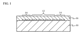
- FIG. 1 is a cross-sectional view of a resonator fabricated to measure a TCF.
- a comb-shaped electrode 12 and reflectors 14 are formed on a piezoelectric substrate 10 made of a LN substrate.
- the reflectors 14 are located at both sides of the comb-shaped electrode 12.
- the comb-shaped electrode 12 and the reflectors 14 mainly include Cu.
- An undoped silicon oxide film 16 is formed on the piezoelectric substrate 10 so as to cover the comb-shaped electrode 12 and the reflectors 14.
- the undoped silicon oxide film 16 is formed by CVD (chemical vapor deposition), and has a film thickness of 0.3 ⁇ .
- ⁇ is the wavelength of an acoustic wave, and corresponds to a pitch between electrode fingers of the comb-shaped electrode 12.
- the undoped silicon oxide film 16 is formed by CVD under various film forming conditions. Changed are temperature, pressure, material gases, flow rate of the material gases, and high-frequency output, which is high frequency power to produce plasma, as the film forming conditions.
- the TCF of an anti-resonance frequency is measured with respect to resonators formed under the various film forming conditions.
- a silicon oxide film, which is formed under the film forming condition same as the undoped silicon oxide film 16, is measured by FTIR (Fourier transform infrared spectroscopy).
- the FTIR method is a measuring method that irradiates a material with infrared light, and then investigates the composition of the material based on absorption of the infrared light, which has energy corresponding to vibration energy of molecules.
- the inventors focus on the absorption waveform of a Si-O stretching vibration in SiO 2 .
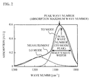
- FIG. 2 is a diagram illustrating FTIR measurement results of the Si-O stretching vibration, and illustrates absorption in arbitrary coordinates versus wave numbers.
- a peak wave number at which the absorption reaches a maximum is measured, and the peak wave number at which the absorption reaches a maximum is indicated by "peak wave number (absorption maximum wave number)".
- the absorption of stretching vibration includes an optical transverse wave (TO) mode and an optical longitudinal wave (LO) mode.
- TO optical transverse wave
- LO optical longitudinal wave
- the absorption of stretching vibration is separated into the TO mode and the LO mode, and a half-value width of the TO mode is measured.
- the peak wave number of the TO mode is indicated by "peak wave number (TO mode peak)”.
- FIG. 3 is a graph of the TCF of the anti-resonance frequency of the resonator versus the peak wave number (absorption maximum wave number) measured by FTIR. Black triangles in FIG. 3 indicate measurement results under various film forming conditions. FIG. 3 reveals that the TCF of the anti-resonance frequency increases and comes closer to 0 as the peak wave number becomes larger, and the TCF is improved.
- FIG. 4 is a graph of the TCF of the anti-resonance frequency of the resonator versus the half-value width of the optical transverse wave (TO) mode measured by FTIR. Black triangles in FIG. 4 indicate measurement results under various film forming conditions. FIG. 4 reveals that the TCF of the anti-resonance frequency increases and comes closer to 0 as the half-value width becomes smaller, and the TCF is improved.
- TO optical transverse wave
- k is a peak wave number
- f is an atomic force between Si and O
- mo is an atomic weight of oxygen
- 0 is a Si-O-Si bonding angle
- e is a permittivity of a silicon oxide film
- ⁇ is a density of the silicon oxide film
- C is a molecular polarizability
- the Si-O-Si bonding angle ⁇ correlates with the permittivity, the density, and the molecular polarizability of the silicon oxide film. Therefore, the peak wave number is related to the permittivity, the density, and the molecular polarizability based on the equation 1 and the equation 2.
- v is a propagation velocity of the acoustic wave
- ( ⁇ v/ ⁇ T) is a rate of change of the propagation velocity v to a temperature T
- ⁇ is a line thermal expansion coefficient
- ( ⁇ v/ ⁇ T) can be obtained from a temperature coefficient of material constant, i.e. a permittivity, a density, a Young's modulus, or the like, of the substrate (or the silicon oxide film).
- material constant of the silicon oxide film such as permittivity, density, or Young's modulus, is related to the TCF.
- the peak wave number of the Si-O stretching vibration is considered to affect the TCF.
- FIG. 3 and FIG. 4 illustrate the TCF of the anti-resonance frequency of the resonator, but the results illustrated in FIG. 3 and FIG. 4 are applicable to the TCF of the resonance frequency of the resonator or the TCF of the frequency characteristic of a filter using the resonator. Also, the results illustrated in FIG. 3 and FIG. 4 are applicable to resonators in the FBAR device and the Lamb wave device, and acoustic wave filters using the resonators in addition to the surface acoustic wave device with the comb-shaped electrode formed on the piezoelectric substrate.
- the TCF of the anti-resonance frequency increases as the peak wave number becomes larger, and the TCF of the anti-resonance frequency increases as the half-value width becomes smaller, in the acoustic wave device using the silicon oxide film as the temperature compensation layer.
- the peak wave number of the B-doped silicon oxide film disclosed in Patent Document I tends to be small compared to that of the undoped silicon oxide film. Therefore, the result presented in FIG 3 reveals that the TCF of the anti-resonance frequency is not improved sufficiently even though the B-doped silicon oxide film is used as the temperature compensation layer instead of the undoped silicon oxide film.
- B does not enter the bonds in SiO 2 , and exists as B 2 O 3 , i.e. impurities, in SiO 2 . That is to say, B does not displace O in the Si-O bond, but displaces Si.
- B does not enter the bonds in SiO 2 , and exists as B 2 O 3 , i.e. impurities, in SiO 2 . That is to say, B does not displace O in the Si-O bond, but displaces Si.
- an attenuation coefficient becomes large in a glass to which B 2 O 3 is added.
- the B-doped silicon oxide film has an effect to increase the attenuation of the acoustic wave.
- the acoustic wave propagates in a film thickness direction of the B-doped silicon oxide film in the FBAR device disclosed in Patent Document 1.
- the film thickness of the B-doped silicon oxide film is thin. Therefore, the distance of the B-doped silicon oxide film through which the acoustic wave propagates is short, and the attenuation of the acoustic wave is small.
- the acoustic wave propagates in a direction perpendicular to the film thickness direction of the B-doped silicon oxide film in the acoustic wave device in which the silicon oxide film is formed so as to cover the comb-shaped electrode as illustrated in FIG. 1 . This increases the distance of the B-doped silicon oxide film through which the acoustic wave propagates, and thus causes the attenuation of the acoustic wave to become large.
- An acoustic wave device of a first embodiment is an exemplary resonator in an acoustic wave device with a comb-shaped electrode located on a piezoelectric substrate, and can be used in surface acoustic wave devices, Love wave devices, and boundary acoustic wave devices for example.
- FIG. 5A is a top view of the acoustic wave device in accordance with the first embodiment
- FIG. 5B is a cross-sectional view taken along line A-A in FIG. 5A .
- reflectors 24 are located at both sides of a comb-shaped electrode 22.
- the comb-shaped electrode 22 is an electrode that excites the acoustic wave, and in which two electrodes for input and output face each other so that respective electrode fingers are arranged alternately.
- the comb-shaped electrode 22 and the reflectors 24 mainly include Cu.
- the comb-shaped electrode 22 and the reflectors 24 are formed on a piezoelectric substrate 20 made of a 0-degree rotation Y-cut LN substrate.
- An F (fluorine)-doped silicon oxide film (e.g. SiOF film) 26 is formed on the piezoelectric substrate 20 so as to cover the comb-shaped electrode 22 and the reflectors 24.
- the F-doped silicon oxide film 26 can be formed by CVD using SiH 4 ,N 2 O, and C 2 F 6 for material gases, and an F content can be adjusted using the flow rate ratio of the material gases.
- the F-doped silicon oxide film 26 preferably has a film thickness thicker than that of the comb-shaped electrode 22 to improve the TCF of the anti-resonance frequency and the like.
- the film thickness of the F-doped silicon oxide film 26 between the electrode fingers is preferably thicker than that of the comb-shaped electrode 22.
- the first embodiment sets the film thickness of the F-doped silicon oxide film 26 to 0.3 ⁇ . ⁇ is the wavelength of the acoustic wave, and corresponds to a pitch between electrode fingers of the comb-shaped electrode 22.
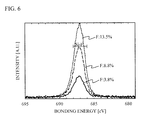
- the XPS (X-ray photoemission spectroscopy) measurement is conducted on the F-doped silicon oxide film to examine how F is incorporated into the silicon oxide film when the silicon oxide film is doped with F.
- the XPS measurement is conducted on three silicon oxide films with respective F contents of 3.8%, 8.8%, and 13.5%.
- FIG. 6 is a diagram illustrating the XPS measurement results, and illustrates intensity in arbitrary coordinates versus bonding energy.
- the XPS measurement results in FIG. 6 indicate that F displaces O in the Si-O bond and forms a Si-F bond when the silicon oxide film is doped with F, and that the Si-F bond increases as the F content increases.
- the respective F-doped silicon oxide films 26 of which have F contents of 2.1 %, 3.8%, and 8.8% are fabricated with respect to the resonator of the first embodiment.
- a resonator is fabricated as the comparative example by using the production condition same as that of the resonator of the first embodiment except that C 2 F 6 gas, which is a source of F, is not used.
- FIG. 7 is a graph of an increment in peak wave number (absorption maximum wave number) and a half-value width of the optical transverse wave (TO) mode normalized by the half-value width of the optical transverse wave (TO) mode of the undoped silicon oxide film versus an F content.
- black rectangles indicate measurement results of the peak wave number
- black triangles indicate measurement results of the half-value width
- approximated lines of them are presented. As illustrated in FIG. 7 , the peak wave number increases and the half-value width decreases as the F content increases.
- FIG. 8 is a diagram illustrating measurement results of frequency characteristics of the resonators of the first embodiment and the comparative example, and illustrates admittance versus frequency normalized by the anti-resonance frequency of the resonator of the comparative example. As illustrated in FIG.
- the anti-resonance frequency of the resonator of the first embodiment which uses the F-doped silicon oxide film 26 with an F content of 8.8%, results in 0.92 multiple of that of the resonator of the comparative example, and the electromechanical coupling coefficient K 2 results in 0.76 multiple.
- the F-doped silicon oxide film 26 has a small Young's modulus and a slow acoustic velocity compared to the undoped silicon oxide film. That is to say, it is considered that the distribution of acoustic waves therein differs from that in the undoped silicon oxide film significantly and the K 2 changes drastically in the same film thickness because the F-doped silicon oxide film 26 has a slower acoustic velocity.
- FIG. 9 is a diagram illustrating measurement results of the K 2 at various film thicknesses of the F-doped silicon oxide film 26, and illustrates the K 2 normalized by the K 2 of the resonator of the comparative example versus the film thickness of the silicon oxide film.
- a black circle indicates the K 2 of the resonator of the comparative example, and white squares indicate the K 2 at various film thickensses of the F-doped silicon oxide film 26.
- the K 2 increases as the film thickness of the F-doped silicon oxide film 26 becomes thinner. This suggests that the resonator of the first embodiment can obtain the K 2 approximately equal to that of the resonator of the comparative example, which uses the undoped silicon oxide film with a film thickness equal to the unreduced film thickness of the F-doped silicon oxide film 26, by reducing the film thickness of the F-doped silicon oxide film 26.
- FIG. 10 is a graph of an increment in TCF versus an F content of the F-doped silicon oxide film 26. As illustrated in FIG. 10 , the TCF increases as the F content increases.
- the TCF increases by 1 ppm/°C
- the TCF increases by 2.9 ppm/°C
- the F content is 8.8%
- the TCF increases by 6.5 ppm/°C. This is assumed to be due to the increase in the peak wave number and the decrease in the half-value width with increase in the F content caused by doping the silicon oxide film with F as illustrated in FIG. 7 .
- the first embodiment forms the comb-shaped electrode 22 and the reflectors 24, which excite the acoustic wave, on the piezoelectric substrate 20 (piezoelectric substance), and forms the F-doped silicon oxide film 26 on the piezoelectric substrate 20 so as to cover the comb-shaped electrode 22 and the reflectors 24.
- F displaces O in the Si-O bond, and forms the Si-F bond. That is to say, F displaces O in a siloxane (Si-O-Si) network or in a Si-O covalent bond, and is incorporated into the bond in SiO 2 as a terminated group Si-F.
- Si-O-Si siloxane
- the peak wave number (absorption maximum wave number) of the Si-O bond stretching vibration can be made to be large, and the half-value width of the optical transverse wave (TO) mode of the Si-O bond stretching vibration can be made to be small by forming the F-doped silicon oxide film 26, which is doped with F displacing O in the Si-O bond, so as to cover the comb-shaped electrode 22, compared to forming the undoped silicon oxide film.
- the TCF increases as the peak wave number (absorption maximum wave number) becomes larger and the half-value width of the optical transverse wave (TO) mode becomes smaller. Therefore, the first embodiment can increase the TCF by using the F-doped silicon oxide film 26 as described in FIG. 10 , and thus can improve the TCF.
- the F-doped silicon oxide film 26 Since F with which the silicon oxide film is doped is incorporated into the bond in SiO 2 as a terminated group Si-F, it does not exist in SiO 2 as impurities. Thus, the F-doped silicon oxide film 26 has a small effect in attenuating the acoustic wave, and therefore, the acoustic wave is little attenuated even though the F-doped silicon oxide film 26 is provided so as to cover the comb-shaped electrode 22. Therefore, the first embodiment can suppress the attenuation of the acoustic wave.
- the first embodiment uses the F-doped silicon oxide film 26 for the silicon oxide film formed so as to cover the comb-shaped electrode 22, but does not intend any limitation.
- a silicon oxide film doped with an element or molecule that displaces O in the Si-O bond may be used.
- the silicon oxide film may be doped with a single kind of element or molecule, or may be doped with two or more kinds of element or molecule.
- the silicon oxide film doped with an element or molecule is preferably doped with an element or molecule that makes the peak wave number (absorption maximum wave number) of the Si-O bond stretching vibration larger than that of the silicon oxide film not doped with the element or molecule because the TCF increases as the peak wave number (absorption maximum wave number) of the Si-O bond stretching vibration becomes larger as described in FIG. 3 .
- the silicon oxide film doped with an element or molecule is preferably doped with an element or molecule that makes the half-value width of the optical transverse wave (TO) mode of the Si-O bond stretching vibration smaller than that of the silicon oxide film not doped with the element or molecule because the TCF increases as the half-value width of the optical transverse wave (TO) mode of the Si-O bond stretching vibration becomes smaller as described in FIG. 4 .
- H, CH 3 ,CH 2 ,F, Cl, C,N, P, and S are examples of the element or molecule that makes the peak wave number of the Si-O bond stretching vibration large, and the half-value width of the TO mode small. Therefore, the silicon oxide film doped with an element of molecule is preferably doped with any one of H, CH 3 ,CH 2 ,F, Cl, C,N, P, and S (collectively referred to as "R") to displace O, and is preferably a silicon oxide film having a Si-R covalent bond. In addition, it preferably has a terminated group of Si-H, Si-CH 3 ,Si-F, Si-Cl, Si-C, Si-N, Si-P, or Si-S.
- a Si-H based material is referred to as HSQ (Hydrogen Silsesquioxane)
- a Si-CH 3 based material is referred to as SiOC, SiOCH, or OSG (Organo Silica Glass)
- a Si-F based material is referred to as SiOF or FSG (Fluorinated Silica Glass)
- a Si-Cl based material is referred to as Chlorinated Silica.
- the increase in TCF and the decrease in K 2 in the silicon oxide film doped with an element or molecule means the increase in energy confinement volume of the acoustic wave in the silicon oxide film. This is due to the slow acoustic velocity in the silicon oxide film doped with the element or molecule. Therefore, the silicon oxide film doped with an element or molecule preferably has a slow acoustic velocity to increase the TCF, and, for example, preferably has an acoustic velocity slower than that in the undoped silicon oxide film.
- E is a Young's modulus
- ⁇ is a density.
- the silicon oxide film doped with an element or molecule preferably has a small Young's modulus E, and for example, preferably has a Young's modulus E smaller than that of the undoped silicon oxide film.
- the K 2 of the resonator using the F-doped silicon oxide film 26 is smaller than the K 2 of the resonator using the undoped silicon oxide film having a film thickness equal to that of the F-doped silicon oxide film 26 (film thickness: 0.3 ⁇ ).
- the resonator using the F-doped silicon oxide film 26 preferably has a K 2 approximately equal to the K 2 of the resonator using the undoped silicon oxide film.
- the K 2 increases as the film thickness of the F-doped silicon oxide film 26 is thinned.
- the F-doped silicon oxide film 26 preferably has a film thickness thinner than the film thickness 0.3 ⁇ of the undoped silicon oxide film to recover the decreasing K 2 . That is to say, the silicon oxide film doped with an element or molecule preferably has a film thickness thinner than that of the undoped silicon oxide film having a given film thickness to recover the K 2 , which becomes smaller than that of the undoped silicon oxide film with the given film thickness, by doping the undoped silicon oxide film having the given film thickness with the element or molecule.
- the first embodiment uses SiH 4 , N 2 O, and C 2 F 6 for the material gases in forming the F-doped silicon oxide film 26, but does not intend any limitation.
- tetraethoxysilane (TEOS), or SiF 4 may be used as a source of Si besides SiH 4 .
- CF 4 , NF 3 , F 2 , HF, SF 6 , ClF 3 , BF 3 , BrF 3 , SF 4 , SiF 4 , NF 2 Cl, FSiH 2 , or F 3 SiH may be used as a source of F besides C 2 F 6 .
- the piezoelectric substrate 20 may be made of LT, ZnO, KNbO 3 , or LBO besides LN.
- the comb-shaped electrode 22 and the reflectors 24 may be made of a metal material mainly including Al, Au, Ag, W, Ta, Pt, Mo, Ni, Co, Cr, Fe, Mn, or Ti besides Cu.
- F may react with water, and produce HF.
- the electrode is preferably made of a metal material, such as Cu, Au, Ag, W, Pt, Mo, Ni, or Cr, which does not react with HF.
- a heat treatment such as an annealing treatment is preferably performed on the silicon oxide film doped with an element or molecule because it improves the filter characteristics.
- the first embodiment measures the peak wave number of the Si-O bond stretching vibration and the half-value width of the optical transverse wave (TO) mode of the Si-O bond stretching vibration by FTIR, but the Raman spectroscopy may be used besides FTIR.
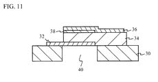
- FIG. 11 is a cross-sectional view of the acoustic wave device of the second embodiment.
- a lower electrode 32 made of, for example, Cu is located on a substrate 30 made of Si (silicon) for example.
- a piezoelectric film 34 made of, for example, AIN(aluminum nitride) is located on the lower electrode 32.
- An upper electrode 36 made of, for example, Cu is located on the piezoelectric film 34 so as to have a portion (resonance portion) that faces the lower electrode 32 across the piezoelectric film 34.
- An F-doped silicon oxide film 38 is located between the piezoelectric film 34 and the upper electrode 36 and in a region in which the lower electrode 32 and the upper electrode 36 face each other.
- a space 40 is located in the substrate 30 in the region in which the lower electrode 32 and the upper electrode 36 face each other.
- the TCF increases as the peak wave number becomes larger, and the TCF increases as the half-value width becomes smaller as described in FIG. 3 and FIG. 4 of the first embodiment.
- the peak wave number increases and the half-value width decreases by forming the F-doped silicon oxide film 38 in the region in which the lower electrode 32 and the upper electrode 36, which excite the acoustic wave, are located across the piezoelectric film 34 (piezoelectric substance) as illustrated in FIG.11 . Therefore, the second embodiment can increase the TCF, and thus improve the TCF.
- FIG. 12A through FIG 12C are cross-sectional views of acoustic wave devices in accordance with first through third variations of the second embodiment.
- the F-doped silicon oxide films 38 are located between the substrate 30 and the lower electrode 32 and between the piezoelectric film 34 and the upper electrode 36, and in the region in which the lower electrode 32 and the upper electrode 36 face each other in the acoustic wave device of the first variation of the second embodiment.
- the F-doped silicon oxide films 38 are located between the substrate 30 and the lower electrode 32 and on the upper electrode 36, and in the region in which the lower electrode 32 and the upper electrode 36 face each other in the acoustic wave device of the second variation of the second embodiment.
- the F-doped silicon oxide film 38 is sandwiched by the piezoelectric films 34 and located in the region in which the lower electrode 32 and the upper electrode 36 face each other in the acoustic wave device of the third variation of the second embodiment.
- the acoustic wave devices of the first through third variations of the second embodiment can also increase the TCF, and thus improve the TCF because the F-doped silicon oxide film 38 is located in the region where the lower electrode 32 and the upper electrode 36 face each other.
- the second embodiment may use a silicon oxide film doped with an element or molecule that displaces O in the Si-O bond besides the F-doped silicon oxide film 38.
- the second embodiment may use ZnO, PZT, or PbTiO 2 for the piezoelectric film 34 besides AIN.
- the substrate 30 may be made of a glass or GaAs besides Si.
- the lower electrode 32 and the upper electrode 36 may be made of a metal material such as Al, Au, Ag, Mo, W, Ta, Pt, Ru, Rh, Ir, Ni, Cr, or Ti besides Cu.
- the lower electrode 32 and the upper electrode 36 are preferably made of a metal material, such as Cu, Au, Ag, W, Pt, Mo, Ni, or Cr, which does not react with HF.
- the second embodiment forms the space 40 by removing the substrate 30 in the region where the lower electrode 32 and the upper electrode 36 face each other, but does not intend any limitation.
- the space 40 may be formed by providing a concave portion to the substrate 30, or the space 40 may be formed above the substrate 30 and between the substrate 30 and the lower electrode 32.
- an acoustic multilayered film which is formed by alternately stacking a film having a high acoustic impedance and a film having a low acoustic impedance with a film thickness of ⁇ /4, may be formed instead of the space 40.
- the second embodiment describes the exemplary FBAR device, but may be adopted to a Lamb wave device in which a lower electrode, a piezoelectric film, and an upper comb-shaped electrode are stacked.
- the Lamb wave device can increase the TCF, and thus improve the TCF by providing a silicon oxide film doped with an element or molecule displacing O in the Si-O bond in a region where the lower electrode and the upper comb-shaped electrode face each other.
- the first embodiment and the second embodiment are the exemplary resonators, but may be a ladder-type filter or a multimode type filter using these resonators.
Landscapes
- Physics & Mathematics (AREA)
- Acoustics & Sound (AREA)
- Surface Acoustic Wave Elements And Circuit Networks Thereof (AREA)
- Piezo-Electric Or Mechanical Vibrators, Or Delay Or Filter Circuits (AREA)
Abstract
Description
- The present invention relates to an acoustic wave device.
- There has been known a surface acoustic wave device, which includes a comb-shaped electrode formed of IDTs (Interdigital Transducer) formed on a surface of a piezoelectric substrate, an FBAR (Film Bulk Acoustic Resonator) device, in which a lower electrode, a piezoelectric film, and an upper electrode are stacked on a substrate, and a Lamb wave device, in which a lower electrode, a piezoelectric film, and an upper comb-shaped electrode are stacked, as acoustic wave devices using acoustic waves. These acoustic wave devices are small and light, can obtain high attenuation, and thus are used as filters of wireless devices such as mobile phone terminals.
- There has been known that the TCF can also be made small in the FBAR device by providing a silicon oxide film in a region in which the lower electrode and the upper electrode face each other (e.g. Non Patent Document 1). In addition, there has been known that the TCF can also be made small in the Lamb wave device by providing a silicon oxide film under the lower electrode (e.g. Non Patent Document 2).
- Moreover, there has been known using a silicon oxide film doped with B (boron) as a temperature compensation layer in the FBAR device (e.g. Patent Document 1).
- Non Patent Document 1: K.M Lakin and three others, "Temperature Coefficient and Ageing of BAW Composite Materials", TFR Technologies, Inc.
- Non Patent Document 2: Chin-Ming Lin and five others, "Thermally compensated aluminum nitride Lamb wave resonators for high temperature applications", APPLIED PHYSICS LETTERS 97, 083501 (2010)
- Patent Document 1: Japanese Patent Application Publication No.
2007-159123 - Patent Document I uses the silicon oxide film doped with B as the temperature compensation layer, but has a problem that even the use of the silicon oxide film doped with B fails to improve a temperature dependence of frequency sufficiently.
- The present invention was made in view of the above problems, and has an object of providing an acoustic wave device capable of improving a temperature dependence of frequency.
- The present invention provides an acoustic wave device including: a piezoelectric substance; an electrode that excites an acoustic wave and is located on the piezoelectric substrate, or electrodes that excite an acoustic wave and are located so as to sandwich the piezoelectric substance; and a silicon oxide film that is doped with an element or molecule displacing O in a Si-O bond, and is located so as to cover the electrode located on the piezoelectric substrate or is located in a region where the electrodes sandwiching the piezoelectric substance face each other. The present invention enables to improve a temperature dependence of frequency.
- With the above configuration, the silicon oxide film doped with an element or molecule may be doped with an element or molecule that makes a half-value width of an optical transverse wave mode of a Si-O bond stretching vibration smaller than that of a silicon oxide film that is not doped with the element or molecule.
- With the above configuration, the silicon oxide film doped with an element or molecule may be doped with an element or molecule that makes a peak wave number of a Si-O bond stretching vibration larger than that of a silicon oxide film that is not doped with the element or molecule.
- With the above configuration, the silicon oxide film doped with an element or molecule may have a Young's modulus smaller than that of an undoped silicon oxide film.
- With the above configuration, the silicon oxide film doped with an element or molecule may have an acoustic velocity slower than that of an undoped silicon oxide film.
- With the above configuration, the silicon oxide film doped with an element or molecule may be doped with two or more kinds of element of molecule.
- With the above configuration, the silicon oxide film doped with an element or molecule may be doped with F.
- With the above configuration, the electrode or the electrodes may be made of Cu, Au, Ag, W, Pt, Mo, Ni, or Cr.
- With the above configuration, the silicon oxide film doped with an element or molecule may be formed by CVD.
- With the above configuration, the electrode may be a comb-shaped electrode located on the piezoelectric substance, and the silicon oxide film doped with an element or molecule may be located so as to cover the comb-shaped electrode located on the piezoelectric substance.
- The present invention enables to improve a temperature dependence of frequency.
-
-
FIG. 1 is a cross-sectional view of a resonator; -
FIG. 2 is a diagram illustrating FTIR measurement results of a Si-O stretching vibration; -
FIG. 3 is a graph of a TCF of an anti-resonance frequency of the resonator versus a peak wave number (absorption maximum wave number); -
FIG. 4 is a graph of the TCF of the anti-resonance frequency of the resonator versus a half-value width of an optical transverse wave (TO) mode; -
FIG. 5A is a top view of an acoustic wave device in accordance with a first embodiment, andFIG. 5B is a cross-sectional view taken along line A-A inFIG. 5A ; -
FIG. 6 is a diagram illustrating XPS measurement results; -
FIG. 7 is a graph of an increment in peak wave number (absorption maximum wave number) and the half-value width of the optical transverse wave (TO) mode normalized by that of an undoped silicon oxide film versus an F content; -
FIG. 8 is a diagram illustrating measurement results of frequency characteristics of resonators in accordance with the first embodiment and a comparative example; -
FIG. 9 is a diagram illustrating measurement results of K2 at various film thicknesses of an F-doped silicon oxide film; -
FIG. 10 is a graph of an increment in TCF versus an F content of the F-doped silicon oxide film; -
FIG. 11 is a cross-sectional view of an acoustic wave device in accordance with a second embodiment; and -
FIG. 12A through FIG. 12C are cross-sectional views of acoustic wave devices in accordance with first through third variations of the second embodiment. - A description will be first given of an experiment conducted by the inventors.
FIG. 1 is a cross-sectional view of a resonator fabricated to measure a TCF. As illustrated inFIG. 1 , a comb-shaped electrode 12 andreflectors 14 are formed on apiezoelectric substrate 10 made of a LN substrate. Thereflectors 14 are located at both sides of the comb-shaped electrode 12. The comb-shaped electrode 12 and thereflectors 14 mainly include Cu. An undoped silicon oxide film 16 is formed on thepiezoelectric substrate 10 so as to cover the comb-shaped electrode 12 and thereflectors 14. The undoped silicon oxide film 16 is formed by CVD (chemical vapor deposition), and has a film thickness of 0.3λ. λ is the wavelength of an acoustic wave, and corresponds to a pitch between electrode fingers of the comb-shaped electrode 12. - The undoped silicon oxide film 16 is formed by CVD under various film forming conditions. Changed are temperature, pressure, material gases, flow rate of the material gases, and high-frequency output, which is high frequency power to produce plasma, as the film forming conditions. The TCF of an anti-resonance frequency is measured with respect to resonators formed under the various film forming conditions. A silicon oxide film, which is formed under the film forming condition same as the undoped silicon oxide film 16, is measured by FTIR (Fourier transform infrared spectroscopy). The FTIR method is a measuring method that irradiates a material with infrared light, and then investigates the composition of the material based on absorption of the infrared light, which has energy corresponding to vibration energy of molecules. Here, the inventors focus on the absorption waveform of a Si-O stretching vibration in SiO2.
-
FIG. 2 is a diagram illustrating FTIR measurement results of the Si-O stretching vibration, and illustrates absorption in arbitrary coordinates versus wave numbers. A peak wave number at which the absorption reaches a maximum is measured, and the peak wave number at which the absorption reaches a maximum is indicated by "peak wave number (absorption maximum wave number)". The absorption of stretching vibration includes an optical transverse wave (TO) mode and an optical longitudinal wave (LO) mode. Thus, as illustrated inFIG. 2 , the absorption of stretching vibration is separated into the TO mode and the LO mode, and a half-value width of the TO mode is measured. The peak wave number of the TO mode is indicated by "peak wave number (TO mode peak)". -
FIG. 3 is a graph of the TCF of the anti-resonance frequency of the resonator versus the peak wave number (absorption maximum wave number) measured by FTIR. Black triangles inFIG. 3 indicate measurement results under various film forming conditions.FIG. 3 reveals that the TCF of the anti-resonance frequency increases and comes closer to 0 as the peak wave number becomes larger, and the TCF is improved. -
FIG. 4 is a graph of the TCF of the anti-resonance frequency of the resonator versus the half-value width of the optical transverse wave (TO) mode measured by FTIR. Black triangles inFIG. 4 indicate measurement results under various film forming conditions.FIG. 4 reveals that the TCF of the anti-resonance frequency increases and comes closer to 0 as the half-value width becomes smaller, and the TCF is improved. - Here, a description will be given of a supposable reason why the peak wave number affects the TCF. According to the Central-force network model (J. Vac. Sci. Technol. Vol. B5, pp 530-537 (1987)), the peak wave number of the Si-O stretching vibration has been known to depend on a Si-O bonding angle as expressed by a following equation.

- Here, k is a peak wave number, f is an atomic force between Si and O, mo is an atomic weight of oxygen, and 0 is a Si-O-Si bonding angle.
- In addition, based on the Lorentz-Lorenz relationship, a relationship among a permittivity, a density, and a molecular polarizability is expressed by a following equation.

- Here, e is a permittivity of a silicon oxide film, ρ is a density of the silicon oxide film, and C is a molecular polarizability.
- The Si-O-Si bonding angle θ correlates with the permittivity, the density, and the molecular polarizability of the silicon oxide film. Therefore, the peak wave number is related to the permittivity, the density, and the molecular polarizability based on the
equation 1 and theequation 2. - The TCF is expressed as follows using a velocity of the acoustic wave at room temperature (25 °C).

- Here, v is a propagation velocity of the acoustic wave, (δv/δT) is a rate of change of the propagation velocity v to a temperature T, and α is a line thermal expansion coefficient.
- According to "Temperature-compensated surface-acoustic-wave devices with SiO2 film overlays" J. Appl. Phys. Vol. 50, No. 3, pp 1360-1369 (1979), (δv/δT) can be obtained from a temperature coefficient of material constant, i.e. a permittivity, a density, a Young's modulus, or the like, of the substrate (or the silicon oxide film). As described above, the material constant of the silicon oxide film, such as permittivity, density, or Young's modulus, is related to the TCF.
- As described above, according to the
equation 1 to theequation 3, the peak wave number of the Si-O stretching vibration is considered to affect the TCF. -
FIG. 3 andFIG. 4 illustrate the TCF of the anti-resonance frequency of the resonator, but the results illustrated inFIG. 3 andFIG. 4 are applicable to the TCF of the resonance frequency of the resonator or the TCF of the frequency characteristic of a filter using the resonator. Also, the results illustrated inFIG. 3 andFIG. 4 are applicable to resonators in the FBAR device and the Lamb wave device, and acoustic wave filters using the resonators in addition to the surface acoustic wave device with the comb-shaped electrode formed on the piezoelectric substrate. - As illustrated in
FIG. 3 andFIG. 4 , the TCF of the anti-resonance frequency increases as the peak wave number becomes larger, and the TCF of the anti-resonance frequency increases as the half-value width becomes smaller, in the acoustic wave device using the silicon oxide film as the temperature compensation layer. For example, according to "Refractive index behavior of boron-doped silica films by plasma-enhanced chemical vapor deposition" Applied Surface Science 92 pp 387-390 (1996), the peak wave number of the B-doped silicon oxide film disclosed in Patent Document I tends to be small compared to that of the undoped silicon oxide film. Therefore, the result presented inFIG 3 reveals that the TCF of the anti-resonance frequency is not improved sufficiently even though the B-doped silicon oxide film is used as the temperature compensation layer instead of the undoped silicon oxide film. - In addition, in the B-doped silicon oxide film, B does not enter the bonds in SiO2, and exists as B2O3, i.e. impurities, in SiO2. That is to say, B does not displace O in the Si-O bond, but displaces Si. According to "Ultrasonic Characterization of Silicate Glasses", IEICE technical report, US 98-50, an attenuation coefficient becomes large in a glass to which B2O3 is added. As described above, the B-doped silicon oxide film has an effect to increase the attenuation of the acoustic wave. For example, the acoustic wave propagates in a film thickness direction of the B-doped silicon oxide film in the FBAR device disclosed in
Patent Document 1. The film thickness of the B-doped silicon oxide film is thin. Therefore, the distance of the B-doped silicon oxide film through which the acoustic wave propagates is short, and the attenuation of the acoustic wave is small. On the other hand, the acoustic wave propagates in a direction perpendicular to the film thickness direction of the B-doped silicon oxide film in the acoustic wave device in which the silicon oxide film is formed so as to cover the comb-shaped electrode as illustrated inFIG. 1 . This increases the distance of the B-doped silicon oxide film through which the acoustic wave propagates, and thus causes the attenuation of the acoustic wave to become large. - Hereinafter, a description will be given of embodiments of an acoustic wave device capable of improving a temperature dependence of frequency.
- An acoustic wave device of a first embodiment is an exemplary resonator in an acoustic wave device with a comb-shaped electrode located on a piezoelectric substrate, and can be used in surface acoustic wave devices, Love wave devices, and boundary acoustic wave devices for example.
FIG. 5A is a top view of the acoustic wave device in accordance with the first embodiment, andFIG. 5B is a cross-sectional view taken along line A-A inFIG. 5A . As illustrated inFIG. 5A ,reflectors 24 are located at both sides of a comb-shapedelectrode 22. The comb-shapedelectrode 22 is an electrode that excites the acoustic wave, and in which two electrodes for input and output face each other so that respective electrode fingers are arranged alternately. The comb-shapedelectrode 22 and thereflectors 24 mainly include Cu. As illustrated inFIG. 5B , the comb-shapedelectrode 22 and thereflectors 24 are formed on apiezoelectric substrate 20 made of a 0-degree rotation Y-cut LN substrate. An F (fluorine)-doped silicon oxide film (e.g. SiOF film) 26 is formed on thepiezoelectric substrate 20 so as to cover the comb-shapedelectrode 22 and thereflectors 24. The F-doped silicon oxide film 26 can be formed by CVD using SiH4,N2O, and C2F6 for material gases, and an F content can be adjusted using the flow rate ratio of the material gases. The F-doped silicon oxide film 26 preferably has a film thickness thicker than that of the comb-shapedelectrode 22 to improve the TCF of the anti-resonance frequency and the like. For example, the film thickness of the F-doped silicon oxide film 26 between the electrode fingers is preferably thicker than that of the comb-shapedelectrode 22. The first embodiment sets the film thickness of the F-doped silicon oxide film 26 to 0.3λ. λ is the wavelength of the acoustic wave, and corresponds to a pitch between electrode fingers of the comb-shapedelectrode 22. - The XPS (X-ray photoemission spectroscopy) measurement is conducted on the F-doped silicon oxide film to examine how F is incorporated into the silicon oxide film when the silicon oxide film is doped with F. The XPS measurement is conducted on three silicon oxide films with respective F contents of 3.8%, 8.8%, and 13.5%.
FIG. 6 is a diagram illustrating the XPS measurement results, and illustrates intensity in arbitrary coordinates versus bonding energy. The XPS measurement results inFIG. 6 indicate that F displaces O in the Si-O bond and forms a Si-F bond when the silicon oxide film is doped with F, and that the Si-F bond increases as the F content increases. - Next, three resonators, the respective F-doped silicon oxide films 26 of which have F contents of 2.1 %, 3.8%, and 8.8%, are fabricated with respect to the resonator of the first embodiment. For example, the F-doped silicon oxide film 26 with an F content of 8.8% is formed by setting the flow rate ratio of SiH4, N2O, and C2F6 to SiH4:N2O:C2F6 = 1:50:3, and the film formation temperature to 270 °C. A resonator is fabricated as the comparative example by using the production condition same as that of the resonator of the first embodiment except that C2F6 gas, which is a source of F, is not used. That is to say, the silicon oxide film covering the comb-shaped electrode is formed to be the undoped silicon oxide film with a film thickness of 0.3λ by CVD using SiH4 and N2O for material gases, and setting the flow rate ratio to SiH4:N2O = 1:50, and the film formation temperature to 270 °C in the resonator of the comparative example.
- First, measured by FTIR are peak wave numbers (absorption maximum wave number) of the Si-O bond stretching vibration and half-value widths of the optical transverse wave (TO) mode with respect to the silicon oxide films formed under the same film forming conditions as those of the three F-doped silicon oxide films 26 with respective F contents of 2.1%, 3.8%, and 8.8%, and the undoped silicon oxide film with an F content of 0%.
FIG. 7 is a graph of an increment in peak wave number (absorption maximum wave number) and a half-value width of the optical transverse wave (TO) mode normalized by the half-value width of the optical transverse wave (TO) mode of the undoped silicon oxide film versus an F content. InFIG. 7 , black rectangles indicate measurement results of the peak wave number, black triangles indicate measurement results of the half-value width, and approximated lines of them are presented. As illustrated inFIG. 7 , the peak wave number increases and the half-value width decreases as the F content increases. - Next, frequency characteristics are measured with respect to the resonator using the F-doped silicon oxide film 26 with an F content of 8.8%, which is one of the three resonators of different F contents of the first embodiment, and the resonator using the undoped silicon oxide film of the comparative example.
FIG. 8 is a diagram illustrating measurement results of frequency characteristics of the resonators of the first embodiment and the comparative example, and illustrates admittance versus frequency normalized by the anti-resonance frequency of the resonator of the comparative example. As illustrated inFIG. 8 , the anti-resonance frequency of the resonator of the first embodiment, which uses the F-doped silicon oxide film 26 with an F content of 8.8%, results in 0.92 multiple of that of the resonator of the comparative example, and the electromechanical coupling coefficient K2 results in 0.76 multiple. This indicates that the F-doped silicon oxide film 26 has a small Young's modulus and a slow acoustic velocity compared to the undoped silicon oxide film. That is to say, it is considered that the distribution of acoustic waves therein differs from that in the undoped silicon oxide film significantly and the K2 changes drastically in the same film thickness because the F-doped silicon oxide film 26 has a slower acoustic velocity. - The behavior of the K2 is investigated by changing the film thickness of the F-doped silicon oxide film 26 in order to make the K2 of the resonator of the first embodiment, which uses the F-doped silicon oxide film 26 with an F content of 8.8%, approximately equal to the K2 of the resonator of the comparative example.
FIG. 9 is a diagram illustrating measurement results of the K2 at various film thicknesses of the F-doped silicon oxide film 26, and illustrates the K2 normalized by the K2 of the resonator of the comparative example versus the film thickness of the silicon oxide film. InFIG. 9 , a black circle indicates the K2 of the resonator of the comparative example, and white squares indicate the K2 at various film thickensses of the F-doped silicon oxide film 26. As illustrated inFIG. 9 , the K2 increases as the film thickness of the F-doped silicon oxide film 26 becomes thinner. This suggests that the resonator of the first embodiment can obtain the K2 approximately equal to that of the resonator of the comparative example, which uses the undoped silicon oxide film with a film thickness equal to the unreduced film thickness of the F-doped silicon oxide film 26, by reducing the film thickness of the F-doped silicon oxide film 26. - Thus, the film thicknesses of the F-doped silicon oxide films 26 are adjusted so that the three above-described resonators with respective F contents of 2.1%, 3.8%, and 8.8% can obtain the K2 approximately equal to that of the resonator of the comparative example, and then the TCF of the anti-resonance frequency is measured with respect to the three resonators.
FIG. 10 is a graph of an increment in TCF versus an F content of the F-doped silicon oxide film 26. As illustrated inFIG. 10 , the TCF increases as the F content increases. When the F content is 2.1%, the TCF increases by 1 ppm/°C, when the F content is 3.8%, the TCF increases by 2.9 ppm/°C, and when the F content is 8.8%, the TCF increases by 6.5 ppm/°C. This is assumed to be due to the increase in the peak wave number and the decrease in the half-value width with increase in the F content caused by doping the silicon oxide film with F as illustrated inFIG. 7 . - As explained above, the first embodiment forms the comb-shaped
electrode 22 and thereflectors 24, which excite the acoustic wave, on the piezoelectric substrate 20 (piezoelectric substance), and forms the F-doped silicon oxide film 26 on thepiezoelectric substrate 20 so as to cover the comb-shapedelectrode 22 and thereflectors 24. When the silicon oxide film is doped with F, as described inFIG. 6 , F displaces O in the Si-O bond, and forms the Si-F bond. That is to say, F displaces O in a siloxane (Si-O-Si) network or in a Si-O covalent bond, and is incorporated into the bond in SiO2 as a terminated group Si-F. As described inFIG. 7 , the peak wave number (absorption maximum wave number) of the Si-O bond stretching vibration can be made to be large, and the half-value width of the optical transverse wave (TO) mode of the Si-O bond stretching vibration can be made to be small by forming the F-doped silicon oxide film 26, which is doped with F displacing O in the Si-O bond, so as to cover the comb-shapedelectrode 22, compared to forming the undoped silicon oxide film. As described inFIG. 3 andFIG. 4 , the TCF increases as the peak wave number (absorption maximum wave number) becomes larger and the half-value width of the optical transverse wave (TO) mode becomes smaller. Therefore, the first embodiment can increase the TCF by using the F-doped silicon oxide film 26 as described inFIG. 10 , and thus can improve the TCF. - Since F with which the silicon oxide film is doped is incorporated into the bond in SiO2 as a terminated group Si-F, it does not exist in SiO2 as impurities. Thus, the F-doped silicon oxide film 26 has a small effect in attenuating the acoustic wave, and therefore, the acoustic wave is little attenuated even though the F-doped silicon oxide film 26 is provided so as to cover the comb-shaped
electrode 22. Therefore, the first embodiment can suppress the attenuation of the acoustic wave. - The first embodiment uses the F-doped silicon oxide film 26 for the silicon oxide film formed so as to cover the comb-shaped
electrode 22, but does not intend any limitation. A silicon oxide film doped with an element or molecule that displaces O in the Si-O bond may be used. The silicon oxide film may be doped with a single kind of element or molecule, or may be doped with two or more kinds of element or molecule. - The silicon oxide film doped with an element or molecule is preferably doped with an element or molecule that makes the peak wave number (absorption maximum wave number) of the Si-O bond stretching vibration larger than that of the silicon oxide film not doped with the element or molecule because the TCF increases as the peak wave number (absorption maximum wave number) of the Si-O bond stretching vibration becomes larger as described in
FIG. 3 . In addition, the silicon oxide film doped with an element or molecule is preferably doped with an element or molecule that makes the half-value width of the optical transverse wave (TO) mode of the Si-O bond stretching vibration smaller than that of the silicon oxide film not doped with the element or molecule because the TCF increases as the half-value width of the optical transverse wave (TO) mode of the Si-O bond stretching vibration becomes smaller as described inFIG. 4 . - H, CH3,CH2,F, Cl, C,N, P, and S are examples of the element or molecule that makes the peak wave number of the Si-O bond stretching vibration large, and the half-value width of the TO mode small. Therefore, the silicon oxide film doped with an element of molecule is preferably doped with any one of H, CH3,CH2,F, Cl, C,N, P, and S (collectively referred to as "R") to displace O, and is preferably a silicon oxide film having a Si-R covalent bond. In addition, it preferably has a terminated group of Si-H, Si-CH3,Si-F, Si-Cl, Si-C, Si-N, Si-P, or Si-S. For example, a Si-H based material is referred to as HSQ (Hydrogen Silsesquioxane), a Si-CH3 based material is referred to as SiOC, SiOCH, or OSG (Organo Silica Glass), a Si-F based material is referred to as SiOF or FSG (Fluorinated Silica Glass), and a Si-Cl based material is referred to as Chlorinated Silica.
- The increase in TCF and the decrease in K2 in the silicon oxide film doped with an element or molecule means the increase in energy confinement volume of the acoustic wave in the silicon oxide film. This is due to the slow acoustic velocity in the silicon oxide film doped with the element or molecule. Therefore, the silicon oxide film doped with an element or molecule preferably has a slow acoustic velocity to increase the TCF, and, for example, preferably has an acoustic velocity slower than that in the undoped silicon oxide film. In addition, in the above presented
equation 3, the propagation velocity v can be expressed by v = (E/p)1/2. Here, E is a Young's modulus, and ρ is a density. This indicates that the TCF becomes larger as the Young's modulus E becomes smaller. Therefore, the silicon oxide film doped with an element or molecule preferably has a small Young's modulus E, and for example, preferably has a Young's modulus E smaller than that of the undoped silicon oxide film. - As described in
FIG. 8 , the K2 of the resonator using the F-doped silicon oxide film 26 is smaller than the K2 of the resonator using the undoped silicon oxide film having a film thickness equal to that of the F-doped silicon oxide film 26 (film thickness: 0.3λ). As different K2s bring concern that the specification is not satisfied, the resonator using the F-doped silicon oxide film 26 preferably has a K2 approximately equal to the K2 of the resonator using the undoped silicon oxide film. As described inFIG. 9 , the K2 increases as the film thickness of the F-doped silicon oxide film 26 is thinned. Therefore, the F-doped silicon oxide film 26 preferably has a film thickness thinner than the film thickness 0.3λ of the undoped silicon oxide film to recover the decreasing K2. That is to say, the silicon oxide film doped with an element or molecule preferably has a film thickness thinner than that of the undoped silicon oxide film having a given film thickness to recover the K2, which becomes smaller than that of the undoped silicon oxide film with the given film thickness, by doping the undoped silicon oxide film having the given film thickness with the element or molecule. - The first embodiment uses SiH4, N2O, and C2F6 for the material gases in forming the F-doped silicon oxide film 26, but does not intend any limitation. For example, tetraethoxysilane (TEOS), or SiF4 may be used as a source of Si besides SiH4. CF4, NF3, F2, HF, SF6, ClF3, BF3, BrF3, SF4, SiF4, NF2Cl, FSiH2, or F3SiH may be used as a source of F besides C2F6.
- In addition, the
piezoelectric substrate 20 may be made of LT, ZnO, KNbO3, or LBO besides LN. The comb-shapedelectrode 22 and thereflectors 24 may be made of a metal material mainly including Al, Au, Ag, W, Ta, Pt, Mo, Ni, Co, Cr, Fe, Mn, or Ti besides Cu. In particular, when the F-doped silicon oxide film 26 is used, F may react with water, and produce HF. Accordingly, the electrode is preferably made of a metal material, such as Cu, Au, Ag, W, Pt, Mo, Ni, or Cr, which does not react with HF. A heat treatment such as an annealing treatment is preferably performed on the silicon oxide film doped with an element or molecule because it improves the filter characteristics. - The first embodiment measures the peak wave number of the Si-O bond stretching vibration and the half-value width of the optical transverse wave (TO) mode of the Si-O bond stretching vibration by FTIR, but the Raman spectroscopy may be used besides FTIR.
- An acoustic wave device in accordance with a second embodiment is an exemplary resonator in an FBAR device.
FIG. 11 is a cross-sectional view of the acoustic wave device of the second embodiment. As illustrated inFIG. 11 , alower electrode 32 made of, for example, Cu is located on asubstrate 30 made of Si (silicon) for example. Apiezoelectric film 34 made of, for example, AIN(aluminum nitride) is located on thelower electrode 32. Anupper electrode 36 made of, for example, Cu is located on thepiezoelectric film 34 so as to have a portion (resonance portion) that faces thelower electrode 32 across thepiezoelectric film 34. An F-dopedsilicon oxide film 38 is located between thepiezoelectric film 34 and theupper electrode 36 and in a region in which thelower electrode 32 and theupper electrode 36 face each other. Aspace 40 is located in thesubstrate 30 in the region in which thelower electrode 32 and theupper electrode 36 face each other. - In the FBAR device, the TCF increases as the peak wave number becomes larger, and the TCF increases as the half-value width becomes smaller as described in
FIG. 3 andFIG. 4 of the first embodiment. As explained inFIG. 7 of the first embodiment, the peak wave number increases and the half-value width decreases by forming the F-dopedsilicon oxide film 38 in the region in which thelower electrode 32 and theupper electrode 36, which excite the acoustic wave, are located across the piezoelectric film 34 (piezoelectric substance) as illustrated inFIG.11 . Therefore, the second embodiment can increase the TCF, and thus improve the TCF. -
FIG. 12A through FIG 12C are cross-sectional views of acoustic wave devices in accordance with first through third variations of the second embodiment. As illustrated inFIG. 12A , the F-dopedsilicon oxide films 38 are located between thesubstrate 30 and thelower electrode 32 and between thepiezoelectric film 34 and theupper electrode 36, and in the region in which thelower electrode 32 and theupper electrode 36 face each other in the acoustic wave device of the first variation of the second embodiment. As illustrated inFIG. 12B , the F-dopedsilicon oxide films 38 are located between thesubstrate 30 and thelower electrode 32 and on theupper electrode 36, and in the region in which thelower electrode 32 and theupper electrode 36 face each other in the acoustic wave device of the second variation of the second embodiment. As illustrated inFIG. 12C , the F-dopedsilicon oxide film 38 is sandwiched by thepiezoelectric films 34 and located in the region in which thelower electrode 32 and theupper electrode 36 face each other in the acoustic wave device of the third variation of the second embodiment. - The acoustic wave devices of the first through third variations of the second embodiment can also increase the TCF, and thus improve the TCF because the F-doped
silicon oxide film 38 is located in the region where thelower electrode 32 and theupper electrode 36 face each other. - The second embodiment may use a silicon oxide film doped with an element or molecule that displaces O in the Si-O bond besides the F-doped
silicon oxide film 38. The second embodiment may use ZnO, PZT, or PbTiO2 for thepiezoelectric film 34 besides AIN. Thesubstrate 30 may be made of a glass or GaAs besides Si. Thelower electrode 32 and theupper electrode 36 may be made of a metal material such as Al, Au, Ag, Mo, W, Ta, Pt, Ru, Rh, Ir, Ni, Cr, or Ti besides Cu. In particular, as described in the first embodiment, when the F-dopedsilicon oxide film 38 is used, thelower electrode 32 and theupper electrode 36 are preferably made of a metal material, such as Cu, Au, Ag, W, Pt, Mo, Ni, or Cr, which does not react with HF. - The second embodiment forms the
space 40 by removing thesubstrate 30 in the region where thelower electrode 32 and theupper electrode 36 face each other, but does not intend any limitation. For example, thespace 40 may be formed by providing a concave portion to thesubstrate 30, or thespace 40 may be formed above thesubstrate 30 and between thesubstrate 30 and thelower electrode 32. In addition, an acoustic multilayered film, which is formed by alternately stacking a film having a high acoustic impedance and a film having a low acoustic impedance with a film thickness of λ/4, may be formed instead of thespace 40. - The second embodiment describes the exemplary FBAR device, but may be adopted to a Lamb wave device in which a lower electrode, a piezoelectric film, and an upper comb-shaped electrode are stacked. The Lamb wave device can increase the TCF, and thus improve the TCF by providing a silicon oxide film doped with an element or molecule displacing O in the Si-O bond in a region where the lower electrode and the upper comb-shaped electrode face each other.
- The first embodiment and the second embodiment are the exemplary resonators, but may be a ladder-type filter or a multimode type filter using these resonators.
- Although the embodiments of the present invention have been described in detail, it should be understood that the present invention is not limited to these specifically described embodiments, and the various change, substitutions, and alterations could be made hereto without departing from the spirit and scope of the invention.
Claims (10)
- An acoustic wave device characterized by comprising:a piezoelectric substance;an electrode that excites an acoustic wave and is located on the piezoelectric substrate, or electrodes that excite an acoustic wave and are located so as to sandwich the piezoelectric substance; anda silicon oxide film that is doped with an element or molecule displacing O in a Si-O bond, and is located so as to cover the electrode located on the piezoelectric substrate or is located in a region where the electrodes sandwiching the piezoelectric substance face each other.
- The acoustic wave device according to claim 1, characterized in that
the silicon oxide film doped with an element or molecule is doped with an element or molecule that makes a half-value width of an optical transverse wave mode of a Si-O bond stretching vibration smaller than that of a silicon oxide film that is not doped with the element or molecule. - The acoustic wave device according to claim 1 or 2, characterized in that
the silicon oxide film doped with an element or molecule is doped with an element or molecule that makes a peak wave number of a Si-O bond stretching vibration larger than that of a silicon oxide film that is not doped with the element or molecule. - The acoustic wave device according to any one of claims 1 through 3, characterized in that
the silicon oxide film doped with an element or molecule has a Young's modulus smaller than that of an undoped silicon oxide film. - The acoustic wave device according to any one of claims 1 through 4, characterized in that
the silicon oxide film doped with an element or molecule has an acoustic velocity slower than that of an undoped silicon oxide film. - The acoustic wave device according to any one of claims 1 through 5, characterized in that
the silicon oxide film doped with an element or molecule is doped with two or more kinds of element of molecule. - The acoustic wave device according to any one of claims 1 through 6, characterized in that
the silicon oxide film doped with an element or molecule is doped with F. - The acoustic wave device according to claim 7 characterized in that the electrode or the electrodes are made of Cu, Au, Ag, W, Pt, Mo, Ni, or Cr.
- The acoustic wave device according to any one of claims 1 through 8, characterized in that
the silicon oxide film doped with an element or molecule is formed by CVD. - The acoustic wave device according to any one of claims 1 through 9, characterized in that
the electrode is a comb-shaped electrode located on the piezoelectric substance, and
the silicon oxide film doped with an element or molecule is located so as to cover the comb-shaped electrode located on the piezoelectric substance.
Applications Claiming Priority (2)
| Application Number | Priority Date | Filing Date | Title |
|---|---|---|---|
| JP2010195020 | 2010-08-31 | ||
| PCT/JP2011/060316 WO2012029354A1 (en) | 2010-08-31 | 2011-04-27 | Acoustic wave device |
Publications (3)
| Publication Number | Publication Date |
|---|---|
| EP2613439A1 true EP2613439A1 (en) | 2013-07-10 |
| EP2613439A4 EP2613439A4 (en) | 2014-06-11 |
| EP2613439B1 EP2613439B1 (en) | 2019-03-13 |
Family
ID=45772467
Family Applications (1)
| Application Number | Title | Priority Date | Filing Date |
|---|---|---|---|
| EP11821372.7A Active EP2613439B1 (en) | 2010-08-31 | 2011-04-27 | Acoustic wave device |
Country Status (6)
| Country | Link |
|---|---|
| US (1) | US8664835B2 (en) |
| EP (1) | EP2613439B1 (en) |
| JP (1) | JP5521045B2 (en) |
| CN (1) | CN103053111B (en) |
| SG (1) | SG186222A1 (en) |
| WO (1) | WO2012029354A1 (en) |
Families Citing this family (25)
| Publication number | Priority date | Publication date | Assignee | Title |
|---|---|---|---|---|
| JP5797979B2 (en) * | 2011-08-31 | 2015-10-21 | 太陽誘電株式会社 | Elastic wave device |
| DE102012105286B4 (en) * | 2012-06-18 | 2018-08-09 | Snaptrack, Inc. | Microacoustic device with TCF compensation layer |
| CN105556840B (en) * | 2013-09-20 | 2019-01-04 | 株式会社村田制作所 | Vibration device and its manufacturing method |
| JP6374653B2 (en) * | 2013-11-18 | 2018-08-15 | 太陽誘電株式会社 | Elastic wave filter and duplexer |
| US9331667B2 (en) * | 2014-07-21 | 2016-05-03 | Triquint Semiconductor, Inc. | Methods, systems, and apparatuses for temperature compensated surface acoustic wave device |
| CN105738471B (en) * | 2014-12-11 | 2018-06-19 | 安徽惠洲地质安全研究院股份有限公司 | A kind of smart electronics tap portable instrument |
| JP6424962B2 (en) * | 2015-06-24 | 2018-11-21 | 株式会社村田製作所 | Filter device |
| US10536133B2 (en) | 2016-04-22 | 2020-01-14 | Avago Technologies International Sales Pte. Limited | Composite surface acoustic wave (SAW) device with absorbing layer for suppression of spurious responses |
| US10177734B2 (en) * | 2015-08-25 | 2019-01-08 | Avago Technologies International Sales Pte. Limited | Surface acoustic wave (SAW) resonator |
| US11228299B2 (en) * | 2017-02-02 | 2022-01-18 | Taiyo Yuden Co., Ltd. | Piezoelectric thin film resonator with insertion film, filter, and multiplexer |
| JP6882929B2 (en) | 2017-05-01 | 2021-06-02 | 太陽誘電株式会社 | Elastic wave resonators, filters and multiplexers |
| JP6869831B2 (en) * | 2017-07-03 | 2021-05-12 | 太陽誘電株式会社 | Piezoelectric thin film resonators and their manufacturing methods, filters and multiplexers |
| JP6781271B2 (en) * | 2017-09-22 | 2020-11-04 | 安徽安努奇科技有限公司Anhui Anuki Technologies Co., Ltd. | Piezoelectric resonator manufacturing method and piezoelectric resonator |
| US12076973B2 (en) | 2018-07-17 | 2024-09-03 | Ii-Vi Delaware, Inc. | Bonded substrate including polycrystalline diamond film |
| US11750169B2 (en) | 2018-07-17 | 2023-09-05 | Ii-Vi Delaware, Inc. | Electrode-defined unsuspended acoustic resonator |
| DE102019115589B4 (en) | 2018-07-17 | 2024-06-13 | Ii-Vi Delaware, Inc. | ELECTRODE LIMITED RESONATOR |
| JP2020096220A (en) * | 2018-12-10 | 2020-06-18 | 株式会社村田製作所 | Acoustic wave device, high-frequency front-end circuit, and communication device |
| JP7288307B2 (en) * | 2019-02-07 | 2023-06-07 | 太陽誘電株式会社 | Acoustic wave device and its manufacturing method, filter and multiplexer |
| TWI810698B (en) * | 2019-06-12 | 2023-08-01 | 美商特拉華公司 | Electrode-defined unsuspended acoustic resonator |
| US11552614B2 (en) | 2019-12-03 | 2023-01-10 | Skyworks Solutions, Inc. | Laterally excited bulk wave device with acoustic mirrors |
| US11463065B2 (en) | 2019-12-03 | 2022-10-04 | Skyworks Solutions, Inc. | Laterally excited bulk wave device with acoustic mirror |
| US20220321088A1 (en) | 2021-03-31 | 2022-10-06 | Skyworks Solutions, Inc. | Acoustic wave device with double side acoustic mirror |
| WO2022226913A1 (en) * | 2021-04-29 | 2022-11-03 | 天津大学 | Piezoelectric mems silicon resonator and electronic device |
| US12615033B2 (en) | 2021-10-04 | 2026-04-28 | Skyworks Solutions, Inc. | Stacked single mirror acoustic wave device and double mirror acoustic wave device |
| US12567854B2 (en) | 2021-10-05 | 2026-03-03 | Skyworks Solutions, Inc. | Stacked acoustic wave device assembly |
Family Cites Families (9)
| Publication number | Priority date | Publication date | Assignee | Title |
|---|---|---|---|---|
| JPS5656025A (en) * | 1979-10-13 | 1981-05-16 | Toshiba Corp | Elastic surface wave resonator |
| JPH0640611B2 (en) * | 1985-03-25 | 1994-05-25 | 株式会社東芝 | Piezoelectric thin film resonator |
| CN1166012C (en) * | 1999-11-11 | 2004-09-08 | 三菱电机株式会社 | Thin-film piezoelectric device |
| FR2848036B1 (en) * | 2002-11-28 | 2005-08-26 | St Microelectronics Sa | SUPPORT FOR ACOUSTIC RESONATOR, ACOUSTIC RESONATOR AND CORRESPONDING INTEGRATED CIRCUIT |
| JP2005252069A (en) * | 2004-03-05 | 2005-09-15 | Tdk Corp | Electronic device and its manufacturing method |
| US7561009B2 (en) * | 2005-11-30 | 2009-07-14 | Avago Technologies General Ip (Singapore) Pte. Ltd. | Film bulk acoustic resonator (FBAR) devices with temperature compensation |
| JP5146197B2 (en) * | 2008-08-21 | 2013-02-20 | 株式会社村田製作所 | Elastic wave device and manufacturing method thereof |
| JP2010088109A (en) * | 2008-09-05 | 2010-04-15 | Panasonic Corp | Acoustic wave element, and electronic equipment using the same |
| JP5207902B2 (en) * | 2008-09-29 | 2013-06-12 | 京セラ株式会社 | Bulk acoustic wave resonators and electronic components |
-
2011
- 2011-04-27 JP JP2012531711A patent/JP5521045B2/en active Active
- 2011-04-27 WO PCT/JP2011/060316 patent/WO2012029354A1/en not_active Ceased
- 2011-04-27 SG SG2012090114A patent/SG186222A1/en unknown
- 2011-04-27 EP EP11821372.7A patent/EP2613439B1/en active Active
- 2011-04-27 CN CN201180037548.8A patent/CN103053111B/en active Active
-
2012
- 2012-12-12 US US13/712,218 patent/US8664835B2/en active Active
Also Published As
| Publication number | Publication date |
|---|---|
| US8664835B2 (en) | 2014-03-04 |
| EP2613439B1 (en) | 2019-03-13 |
| WO2012029354A1 (en) | 2012-03-08 |
| EP2613439A4 (en) | 2014-06-11 |
| JP5521045B2 (en) | 2014-06-11 |
| CN103053111B (en) | 2015-07-22 |
| SG186222A1 (en) | 2013-01-30 |
| CN103053111A (en) | 2013-04-17 |
| JPWO2012029354A1 (en) | 2013-10-28 |
| US20130099630A1 (en) | 2013-04-25 |
Similar Documents
| Publication | Publication Date | Title |
|---|---|---|
| EP2613439B1 (en) | Acoustic wave device | |
| JP5797979B2 (en) | Elastic wave device | |
| CN111416590A (en) | A kind of high frequency acoustic wave resonator and preparation method thereof | |
| CN107404302B (en) | Composite Surface Acoustic Wave (SAW) device having an absorption layer for suppressing spurious signal response | |
| US11916531B2 (en) | Acoustic wave device, filter, and multiplexer | |
| CN112088490A (en) | SAW device with composite substrate for UHF | |
| Matsuda et al. | Correlation between propagation loss and silicon dioxide film properties for surface acoustic wave devices | |
| Matsuda et al. | Use of fluorine-doped silicon oxide for temperature compensation of radio frequency surface acoustic wave devices | |
| JP7340349B2 (en) | Piezoelectric thin film resonator and its manufacturing method, filter and multiplexer | |
| JP7288307B2 (en) | Acoustic wave device and its manufacturing method, filter and multiplexer | |
| JP5417108B2 (en) | Method for manufacturing acoustic wave device | |
| Nishimura et al. | The temperature coefficients of frequency of surface acoustic wave devices with SiO x N y passivation films on LiTaO 3 substrates | |
| JP7754878B2 (en) | Composite substrates for surface acoustic wave devices | |
| JP5892762B2 (en) | Elastic wave device | |
| JP2011139215A (en) | Surface acoustic wave device, oscillator, and module apparatus | |
| US8624690B2 (en) | Surface acoustic wave device, oscillator, module apparatus | |
| US12562712B2 (en) | Ultra-high frequency micro-acoustic device | |
| Matsuda et al. | Application of fluorine doped SiO 2 films for temperature compensated SAW devices | |
| WO2019108758A1 (en) | Alternative temperature compensating materials to amorhphous silica in acoustic wave resonators | |
| Wang et al. | Characteristics of surface acoustic waves based on (110) ZNO/(110) AlN/R-sapphire structure | |
| Kone et al. | Resonator using guided waves in a piezoelectric layer above a Bragg mirror | |
| Moradian et al. | Temperature compensation of MEMS resonators using sputtered fluorine-doped silicon dioxide | |
| JP2011151641A (en) | Surface acoustic wave device, oscillator, and module device | |
| JP2011176546A (en) | Surface acoustic wave device, oscillator, module apparatus | |
| JP2011151642A (en) | Surface acoustic wave device, oscillator, and module device |
Legal Events
| Date | Code | Title | Description |
|---|---|---|---|
| PUAI | Public reference made under article 153(3) epc to a published international application that has entered the european phase |
Free format text: ORIGINAL CODE: 0009012 |
|
| 17P | Request for examination filed |
Effective date: 20130128 |
|
| AK | Designated contracting states |
Kind code of ref document: A1 Designated state(s): AL AT BE BG CH CY CZ DE DK EE ES FI FR GB GR HR HU IE IS IT LI LT LU LV MC MK MT NL NO PL PT RO RS SE SI SK SM TR |
|
| DAX | Request for extension of the european patent (deleted) | ||
| A4 | Supplementary search report drawn up and despatched |
Effective date: 20140509 |
|
| RIC1 | Information provided on ipc code assigned before grant |
Ipc: H03H 9/17 20060101ALI20140502BHEP Ipc: H03H 9/02 20060101AFI20140502BHEP Ipc: H01L 41/04 20060101ALI20140502BHEP Ipc: H03H 9/13 20060101ALI20140502BHEP |
|
| REG | Reference to a national code |
Ref country code: DE Ref legal event code: R079 Ref document number: 602011057190 Country of ref document: DE Free format text: PREVIOUS MAIN CLASS: H03H0009145000 Ipc: H03H0009020000 |
|
| GRAP | Despatch of communication of intention to grant a patent |
Free format text: ORIGINAL CODE: EPIDOSNIGR1 |
|
| STAA | Information on the status of an ep patent application or granted ep patent |
Free format text: STATUS: GRANT OF PATENT IS INTENDED |
|
| RIC1 | Information provided on ipc code assigned before grant |
Ipc: H03H 9/02 20060101AFI20180911BHEP Ipc: H03H 9/17 20060101ALI20180911BHEP Ipc: H03H 9/13 20060101ALI20180911BHEP |
|
| INTG | Intention to grant announced |
Effective date: 20181002 |
|
| GRAS | Grant fee paid |
Free format text: ORIGINAL CODE: EPIDOSNIGR3 |
|
| GRAA | (expected) grant |
Free format text: ORIGINAL CODE: 0009210 |
|
| STAA | Information on the status of an ep patent application or granted ep patent |
Free format text: STATUS: THE PATENT HAS BEEN GRANTED |
|
| AK | Designated contracting states |
Kind code of ref document: B1 Designated state(s): AL AT BE BG CH CY CZ DE DK EE ES FI FR GB GR HR HU IE IS IT LI LT LU LV MC MK MT NL NO PL PT RO RS SE SI SK SM TR |
|
| REG | Reference to a national code |
Ref country code: GB Ref legal event code: FG4D |
|
| REG | Reference to a national code |
Ref country code: CH Ref legal event code: EP Ref country code: AT Ref legal event code: REF Ref document number: 1109070 Country of ref document: AT Kind code of ref document: T Effective date: 20190315 |
|
| REG | Reference to a national code |
Ref country code: IE Ref legal event code: FG4D |
|
| REG | Reference to a national code |
Ref country code: DE Ref legal event code: R096 Ref document number: 602011057190 Country of ref document: DE |
|
| REG | Reference to a national code |
Ref country code: NL Ref legal event code: MP Effective date: 20190313 |
|
| REG | Reference to a national code |
Ref country code: LT Ref legal event code: MG4D |
|
| PG25 | Lapsed in a contracting state [announced via postgrant information from national office to epo] |
Ref country code: FI Free format text: LAPSE BECAUSE OF FAILURE TO SUBMIT A TRANSLATION OF THE DESCRIPTION OR TO PAY THE FEE WITHIN THE PRESCRIBED TIME-LIMIT Effective date: 20190313 Ref country code: NO Free format text: LAPSE BECAUSE OF FAILURE TO SUBMIT A TRANSLATION OF THE DESCRIPTION OR TO PAY THE FEE WITHIN THE PRESCRIBED TIME-LIMIT Effective date: 20190613 Ref country code: SE Free format text: LAPSE BECAUSE OF FAILURE TO SUBMIT A TRANSLATION OF THE DESCRIPTION OR TO PAY THE FEE WITHIN THE PRESCRIBED TIME-LIMIT Effective date: 20190313 Ref country code: LT Free format text: LAPSE BECAUSE OF FAILURE TO SUBMIT A TRANSLATION OF THE DESCRIPTION OR TO PAY THE FEE WITHIN THE PRESCRIBED TIME-LIMIT Effective date: 20190313 |
|
| PG25 | Lapsed in a contracting state [announced via postgrant information from national office to epo] |
Ref country code: RS Free format text: LAPSE BECAUSE OF FAILURE TO SUBMIT A TRANSLATION OF THE DESCRIPTION OR TO PAY THE FEE WITHIN THE PRESCRIBED TIME-LIMIT Effective date: 20190313 Ref country code: HR Free format text: LAPSE BECAUSE OF FAILURE TO SUBMIT A TRANSLATION OF THE DESCRIPTION OR TO PAY THE FEE WITHIN THE PRESCRIBED TIME-LIMIT Effective date: 20190313 Ref country code: NL Free format text: LAPSE BECAUSE OF FAILURE TO SUBMIT A TRANSLATION OF THE DESCRIPTION OR TO PAY THE FEE WITHIN THE PRESCRIBED TIME-LIMIT Effective date: 20190313 Ref country code: BG Free format text: LAPSE BECAUSE OF FAILURE TO SUBMIT A TRANSLATION OF THE DESCRIPTION OR TO PAY THE FEE WITHIN THE PRESCRIBED TIME-LIMIT Effective date: 20190613 Ref country code: GR Free format text: LAPSE BECAUSE OF FAILURE TO SUBMIT A TRANSLATION OF THE DESCRIPTION OR TO PAY THE FEE WITHIN THE PRESCRIBED TIME-LIMIT Effective date: 20190614 Ref country code: LV Free format text: LAPSE BECAUSE OF FAILURE TO SUBMIT A TRANSLATION OF THE DESCRIPTION OR TO PAY THE FEE WITHIN THE PRESCRIBED TIME-LIMIT Effective date: 20190313 |
|
| REG | Reference to a national code |
Ref country code: AT Ref legal event code: MK05 Ref document number: 1109070 Country of ref document: AT Kind code of ref document: T Effective date: 20190313 |
|
| PG25 | Lapsed in a contracting state [announced via postgrant information from national office to epo] |
Ref country code: EE Free format text: LAPSE BECAUSE OF FAILURE TO SUBMIT A TRANSLATION OF THE DESCRIPTION OR TO PAY THE FEE WITHIN THE PRESCRIBED TIME-LIMIT Effective date: 20190313 Ref country code: IT Free format text: LAPSE BECAUSE OF FAILURE TO SUBMIT A TRANSLATION OF THE DESCRIPTION OR TO PAY THE FEE WITHIN THE PRESCRIBED TIME-LIMIT Effective date: 20190313 Ref country code: CZ Free format text: LAPSE BECAUSE OF FAILURE TO SUBMIT A TRANSLATION OF THE DESCRIPTION OR TO PAY THE FEE WITHIN THE PRESCRIBED TIME-LIMIT Effective date: 20190313 Ref country code: RO Free format text: LAPSE BECAUSE OF FAILURE TO SUBMIT A TRANSLATION OF THE DESCRIPTION OR TO PAY THE FEE WITHIN THE PRESCRIBED TIME-LIMIT Effective date: 20190313 Ref country code: PT Free format text: LAPSE BECAUSE OF FAILURE TO SUBMIT A TRANSLATION OF THE DESCRIPTION OR TO PAY THE FEE WITHIN THE PRESCRIBED TIME-LIMIT Effective date: 20190713 Ref country code: AL Free format text: LAPSE BECAUSE OF FAILURE TO SUBMIT A TRANSLATION OF THE DESCRIPTION OR TO PAY THE FEE WITHIN THE PRESCRIBED TIME-LIMIT Effective date: 20190313 Ref country code: SK Free format text: LAPSE BECAUSE OF FAILURE TO SUBMIT A TRANSLATION OF THE DESCRIPTION OR TO PAY THE FEE WITHIN THE PRESCRIBED TIME-LIMIT Effective date: 20190313 Ref country code: ES Free format text: LAPSE BECAUSE OF FAILURE TO SUBMIT A TRANSLATION OF THE DESCRIPTION OR TO PAY THE FEE WITHIN THE PRESCRIBED TIME-LIMIT Effective date: 20190313 |
|
| PG25 | Lapsed in a contracting state [announced via postgrant information from national office to epo] |
Ref country code: SM Free format text: LAPSE BECAUSE OF FAILURE TO SUBMIT A TRANSLATION OF THE DESCRIPTION OR TO PAY THE FEE WITHIN THE PRESCRIBED TIME-LIMIT Effective date: 20190313 Ref country code: PL Free format text: LAPSE BECAUSE OF FAILURE TO SUBMIT A TRANSLATION OF THE DESCRIPTION OR TO PAY THE FEE WITHIN THE PRESCRIBED TIME-LIMIT Effective date: 20190313 |
|
| REG | Reference to a national code |
Ref country code: CH Ref legal event code: PL |
|
| REG | Reference to a national code |
Ref country code: DE Ref legal event code: R097 Ref document number: 602011057190 Country of ref document: DE |
|
| REG | Reference to a national code |
Ref country code: BE Ref legal event code: MM Effective date: 20190430 |
|
| PG25 | Lapsed in a contracting state [announced via postgrant information from national office to epo] |
Ref country code: AT Free format text: LAPSE BECAUSE OF FAILURE TO SUBMIT A TRANSLATION OF THE DESCRIPTION OR TO PAY THE FEE WITHIN THE PRESCRIBED TIME-LIMIT Effective date: 20190313 Ref country code: LU Free format text: LAPSE BECAUSE OF NON-PAYMENT OF DUE FEES Effective date: 20190427 Ref country code: IS Free format text: LAPSE BECAUSE OF FAILURE TO SUBMIT A TRANSLATION OF THE DESCRIPTION OR TO PAY THE FEE WITHIN THE PRESCRIBED TIME-LIMIT Effective date: 20190713 |
|
| PLBE | No opposition filed within time limit |
Free format text: ORIGINAL CODE: 0009261 |
|
| STAA | Information on the status of an ep patent application or granted ep patent |
Free format text: STATUS: NO OPPOSITION FILED WITHIN TIME LIMIT |
|
| PG25 | Lapsed in a contracting state [announced via postgrant information from national office to epo] |
Ref country code: CH Free format text: LAPSE BECAUSE OF NON-PAYMENT OF DUE FEES Effective date: 20190430 Ref country code: DK Free format text: LAPSE BECAUSE OF FAILURE TO SUBMIT A TRANSLATION OF THE DESCRIPTION OR TO PAY THE FEE WITHIN THE PRESCRIBED TIME-LIMIT Effective date: 20190313 Ref country code: LI Free format text: LAPSE BECAUSE OF NON-PAYMENT OF DUE FEES Effective date: 20190430 Ref country code: MC Free format text: LAPSE BECAUSE OF FAILURE TO SUBMIT A TRANSLATION OF THE DESCRIPTION OR TO PAY THE FEE WITHIN THE PRESCRIBED TIME-LIMIT Effective date: 20190313 |
|
| 26N | No opposition filed |
Effective date: 20191216 |
|
| GBPC | Gb: european patent ceased through non-payment of renewal fee |
Effective date: 20190613 |
|
| PG25 | Lapsed in a contracting state [announced via postgrant information from national office to epo] |
Ref country code: BE Free format text: LAPSE BECAUSE OF NON-PAYMENT OF DUE FEES Effective date: 20190430 Ref country code: SI Free format text: LAPSE BECAUSE OF FAILURE TO SUBMIT A TRANSLATION OF THE DESCRIPTION OR TO PAY THE FEE WITHIN THE PRESCRIBED TIME-LIMIT Effective date: 20190313 |
|
| PG25 | Lapsed in a contracting state [announced via postgrant information from national office to epo] |
Ref country code: TR Free format text: LAPSE BECAUSE OF FAILURE TO SUBMIT A TRANSLATION OF THE DESCRIPTION OR TO PAY THE FEE WITHIN THE PRESCRIBED TIME-LIMIT Effective date: 20190313 |
|
| PG25 | Lapsed in a contracting state [announced via postgrant information from national office to epo] |
Ref country code: IE Free format text: LAPSE BECAUSE OF NON-PAYMENT OF DUE FEES Effective date: 20190427 Ref country code: GB Free format text: LAPSE BECAUSE OF NON-PAYMENT OF DUE FEES Effective date: 20190613 |
|
| PG25 | Lapsed in a contracting state [announced via postgrant information from national office to epo] |
Ref country code: FR Free format text: LAPSE BECAUSE OF NON-PAYMENT OF DUE FEES Effective date: 20190513 |
|
| REG | Reference to a national code |
Ref country code: DE Ref legal event code: R082 Ref document number: 602011057190 Country of ref document: DE Representative=s name: HL KEMPNER PATENTANWAELTE, SOLICITORS (ENGLAND, DE Ref country code: DE Ref legal event code: R082 Ref document number: 602011057190 Country of ref document: DE Representative=s name: HL KEMPNER PARTG MBB, DE Ref country code: DE Ref legal event code: R082 Ref document number: 602011057190 Country of ref document: DE Representative=s name: HL KEMPNER PATENTANWALT, RECHTSANWALT, SOLICIT, DE |
|
| PG25 | Lapsed in a contracting state [announced via postgrant information from national office to epo] |
Ref country code: CY Free format text: LAPSE BECAUSE OF FAILURE TO SUBMIT A TRANSLATION OF THE DESCRIPTION OR TO PAY THE FEE WITHIN THE PRESCRIBED TIME-LIMIT Effective date: 20190313 |
|
| PG25 | Lapsed in a contracting state [announced via postgrant information from national office to epo] |
Ref country code: HU Free format text: LAPSE BECAUSE OF FAILURE TO SUBMIT A TRANSLATION OF THE DESCRIPTION OR TO PAY THE FEE WITHIN THE PRESCRIBED TIME-LIMIT; INVALID AB INITIO Effective date: 20110427 Ref country code: MT Free format text: LAPSE BECAUSE OF FAILURE TO SUBMIT A TRANSLATION OF THE DESCRIPTION OR TO PAY THE FEE WITHIN THE PRESCRIBED TIME-LIMIT Effective date: 20190313 |
|
| PG25 | Lapsed in a contracting state [announced via postgrant information from national office to epo] |
Ref country code: MK Free format text: LAPSE BECAUSE OF FAILURE TO SUBMIT A TRANSLATION OF THE DESCRIPTION OR TO PAY THE FEE WITHIN THE PRESCRIBED TIME-LIMIT Effective date: 20190313 |
|
| P01 | Opt-out of the competence of the unified patent court (upc) registered |
Effective date: 20230509 |
|
| PGFP | Annual fee paid to national office [announced via postgrant information from national office to epo] |
Ref country code: DE Payment date: 20250305 Year of fee payment: 15 |