EP2612330B1 - X-ray waveguide - Google Patents
X-ray waveguide Download PDFInfo
- Publication number
- EP2612330B1 EP2612330B1 EP20110763785 EP11763785A EP2612330B1 EP 2612330 B1 EP2612330 B1 EP 2612330B1 EP 20110763785 EP20110763785 EP 20110763785 EP 11763785 A EP11763785 A EP 11763785A EP 2612330 B1 EP2612330 B1 EP 2612330B1
- Authority
- EP
- European Patent Office
- Prior art keywords
- core
- rays
- angle
- cladding
- waveguide
- Prior art date
- Legal status (The legal status is an assumption and is not a legal conclusion. Google has not performed a legal analysis and makes no representation as to the accuracy of the status listed.)
- Not-in-force
Links
- 230000000737 periodic effect Effects 0.000 claims description 81
- 238000005253 cladding Methods 0.000 claims description 68
- 239000000463 material Substances 0.000 claims description 39
- 229910010272 inorganic material Inorganic materials 0.000 claims description 9
- 239000011147 inorganic material Substances 0.000 claims description 9
- CPLXHLVBOLITMK-UHFFFAOYSA-N Magnesium oxide Chemical compound [Mg]=O CPLXHLVBOLITMK-UHFFFAOYSA-N 0.000 claims description 4
- VYPSYNLAJGMNEJ-UHFFFAOYSA-N Silicium dioxide Chemical compound O=[Si]=O VYPSYNLAJGMNEJ-UHFFFAOYSA-N 0.000 claims description 4
- GWEVSGVZZGPLCZ-UHFFFAOYSA-N Titan oxide Chemical compound O=[Ti]=O GWEVSGVZZGPLCZ-UHFFFAOYSA-N 0.000 claims description 4
- 229910052581 Si3N4 Inorganic materials 0.000 claims description 2
- 229910052796 boron Inorganic materials 0.000 claims description 2
- 229910052681 coesite Inorganic materials 0.000 claims description 2
- 229910052906 cristobalite Inorganic materials 0.000 claims description 2
- 229910052741 iridium Inorganic materials 0.000 claims description 2
- 229910052762 osmium Inorganic materials 0.000 claims description 2
- 239000000377 silicon dioxide Substances 0.000 claims description 2
- 229910052682 stishovite Inorganic materials 0.000 claims description 2
- 229910052905 tridymite Inorganic materials 0.000 claims description 2
- 229910004541 SiN Inorganic materials 0.000 claims 1
- PNEYBMLMFCGWSK-UHFFFAOYSA-N aluminium oxide Inorganic materials [O-2].[O-2].[O-2].[Al+3].[Al+3] PNEYBMLMFCGWSK-UHFFFAOYSA-N 0.000 claims 1
- 229910052593 corundum Inorganic materials 0.000 claims 1
- 229910003465 moissanite Inorganic materials 0.000 claims 1
- 229910010271 silicon carbide Inorganic materials 0.000 claims 1
- 229910001845 yogo sapphire Inorganic materials 0.000 claims 1
- 239000011162 core material Substances 0.000 description 82
- 239000010408 film Substances 0.000 description 76
- TWNQGVIAIRXVLR-UHFFFAOYSA-N oxo(oxoalumanyloxy)alumane Chemical compound O=[Al]O[Al]=O TWNQGVIAIRXVLR-UHFFFAOYSA-N 0.000 description 18
- 230000005684 electric field Effects 0.000 description 16
- 238000010586 diagram Methods 0.000 description 15
- 229910052799 carbon Inorganic materials 0.000 description 9
- OKTJSMMVPCPJKN-UHFFFAOYSA-N Carbon Chemical compound [C] OKTJSMMVPCPJKN-UHFFFAOYSA-N 0.000 description 8
- 230000003287 optical effect Effects 0.000 description 8
- 239000000758 substrate Substances 0.000 description 6
- WFKWXMTUELFFGS-UHFFFAOYSA-N tungsten Chemical compound [W] WFKWXMTUELFFGS-UHFFFAOYSA-N 0.000 description 6
- 229910052721 tungsten Inorganic materials 0.000 description 6
- 239000010937 tungsten Substances 0.000 description 6
- 238000000034 method Methods 0.000 description 5
- 238000004544 sputter deposition Methods 0.000 description 5
- INAHAJYZKVIDIZ-UHFFFAOYSA-N boron carbide Chemical compound B12B3B4C32B41 INAHAJYZKVIDIZ-UHFFFAOYSA-N 0.000 description 4
- 230000007423 decrease Effects 0.000 description 4
- 238000010030 laminating Methods 0.000 description 4
- NRNCYVBFPDDJNE-UHFFFAOYSA-N pemoline Chemical compound O1C(N)=NC(=O)C1C1=CC=CC=C1 NRNCYVBFPDDJNE-UHFFFAOYSA-N 0.000 description 4
- 238000010521 absorption reaction Methods 0.000 description 3
- 239000013078 crystal Substances 0.000 description 3
- 230000000694 effects Effects 0.000 description 3
- 238000002474 experimental method Methods 0.000 description 3
- 239000010409 thin film Substances 0.000 description 3
- 229910052580 B4C Inorganic materials 0.000 description 2
- 230000008901 benefit Effects 0.000 description 2
- 239000012141 concentrate Substances 0.000 description 2
- 230000008878 coupling Effects 0.000 description 2
- 238000010168 coupling process Methods 0.000 description 2
- 238000005859 coupling reaction Methods 0.000 description 2
- 230000005672 electromagnetic field Effects 0.000 description 2
- 238000007687 exposure technique Methods 0.000 description 2
- 239000010931 gold Substances 0.000 description 2
- 238000003384 imaging method Methods 0.000 description 2
- 230000005855 radiation Effects 0.000 description 2
- 238000012552 review Methods 0.000 description 2
- 238000002441 X-ray diffraction Methods 0.000 description 1
- 238000013459 approach Methods 0.000 description 1
- 238000006243 chemical reaction Methods 0.000 description 1
- 238000011161 development Methods 0.000 description 1
- 230000018109 developmental process Effects 0.000 description 1
- 239000006185 dispersion Substances 0.000 description 1
- PCHJSUWPFVWCPO-UHFFFAOYSA-N gold Chemical compound [Au] PCHJSUWPFVWCPO-UHFFFAOYSA-N 0.000 description 1
- 229910052737 gold Inorganic materials 0.000 description 1
- 239000007769 metal material Substances 0.000 description 1
- 238000012986 modification Methods 0.000 description 1
- 230000004048 modification Effects 0.000 description 1
- 229910052759 nickel Inorganic materials 0.000 description 1
- 230000008569 process Effects 0.000 description 1
- 230000000644 propagated effect Effects 0.000 description 1
- 230000001902 propagating effect Effects 0.000 description 1
- 239000004065 semiconductor Substances 0.000 description 1
- 238000007493 shaping process Methods 0.000 description 1
- 238000007740 vapor deposition Methods 0.000 description 1
Images


Classifications
-
- G—PHYSICS
- G21—NUCLEAR PHYSICS; NUCLEAR ENGINEERING
- G21K—TECHNIQUES FOR HANDLING PARTICLES OR IONISING RADIATION NOT OTHERWISE PROVIDED FOR; IRRADIATION DEVICES; GAMMA RAY OR X-RAY MICROSCOPES
- G21K1/00—Arrangements for handling particles or ionising radiation, e.g. focusing or moderating
- G21K1/06—Arrangements for handling particles or ionising radiation, e.g. focusing or moderating using diffraction, refraction or reflection, e.g. monochromators
- G21K1/062—Devices having a multilayer structure
-
- G—PHYSICS
- G21—NUCLEAR PHYSICS; NUCLEAR ENGINEERING
- G21K—TECHNIQUES FOR HANDLING PARTICLES OR IONISING RADIATION NOT OTHERWISE PROVIDED FOR; IRRADIATION DEVICES; GAMMA RAY OR X-RAY MICROSCOPES
- G21K2201/00—Arrangements for handling radiation or particles
- G21K2201/06—Arrangements for handling radiation or particles using diffractive, refractive or reflecting elements
- G21K2201/061—Arrangements for handling radiation or particles using diffractive, refractive or reflecting elements characterised by a multilayer structure
Definitions
- the present invention relates to an X-ray waveguide used in an X-ray optical system of an X-ray analysis technique, an X-ray imaging technique, an X-ray exposure technique, and the like.
- a refractive index difference for the electromagnetic wave between different materials is very small, so the total reflection angle is very small. Therefore, to control electromagnetic waves including X-rays, a large-scale spatial optical system has been used, and is still mainly used.
- One of the main components included in the spatial optical system is a multilayer film reflecting mirror in which materials having different refractive indices are alternately laminated.
- the multilayer film reflecting mirror has various functions such as beam shaping, spot size conversion, and wavelength selection.
- a conventional X-ray waveguide tube such as a poly-capillary confines X-rays in the tube and propagates the X-rays.
- an X-ray waveguide is studied, which confines electromagnetic waves in a thin film or a multilayer film and propagates the electromagnetic waves, in order to downsize and enhance the optical system.
- a thin film waveguide is reported in which a guiding layer is sandwiched by a two-layer one-dimensional periodic structure (see NPL 2).
- an X-ray waveguide is reported in which a plurality of thin film X-ray waveguides that confine X-rays by total reflection are laminated and disposed (see NPL 1).
- NPL 1 As a cladding material of each waveguide, Ni, which has small imaginary part of the refractive index and large real part of the refractive index, is used in order to confine X-rays in each laminated waveguide consisting of single guiding layer by total reflection. Therefore, in NPL 1, X-ray propagation loss increases in each cladding. Further, waveguide mode coupling occurs between adjacent waveguides, and thereby many coupled modes are formed in the entire waveguide. Thus there is a problem that a single waveguide mode is difficult to be excited.
- NPL 2 an X-ray waveguide is proposed in which X-rays are confined in a core by Bragg reflection of a multilayer film provided as cladding.
- the multilayer film is formed of Ni and C, and a metal material absorbing a large amount of X-rays is used in many layers, so that a large absorption loss of X-rays occurs in the multilayer film.
- a multilayer film having a very large number of layers needs to be used as cladding in order to confine X-rays in a core by Bragg reflection of the multilayer film as described in the above example.
- the present invention is made in view of the above background art, and provides an X-ray waveguide in which a propagation loss of X-rays is small and a specific single waveguide mode can be selectively excited.
- the present invention provides an X-ray waveguide according to claim 1.
- an X-ray waveguide in which a propagation loss of X-rays is small and a single waveguide mode in phase over the cross section area normal to the direction of propagation constant can be selectively excited.
- an X-ray means an electromagnetic wave in a wavelength band in which the real part of the refractive index of material is smaller than 1.
- the X-ray indicates an electromagnetic wave having a wavelength of 100 nanometer or less including extreme ultraviolet (EUV) light.
- EUV extreme ultraviolet
- the present invention is to control an electromagnetic wave corresponding to the above-described X-ray.
- electromagnetic wave is used synonymously with the X-ray.
- the frequency of an electromagnetic wave having such a short wavelength is very high, and outermost electron of matter cannot respond.
- n of materials for X-rays is generally represented by using a decrement ⁇ from 1 of the real part and the imaginary part ⁇ ' related to absorption as shown in the following formula (1).
- ⁇ is proportional to the electron density ⁇ e of a material, the larger the electron density of the material is, the smaller the real part of the refractive index is.
- the real part of the refractive index n' is 1- ⁇ .
- the electron density ⁇ e is proportional to the atom density ⁇ a and the atomic number Z.
- the refractive index of materials for X-rays is represented by a complex number.
- the real part n' is referred to as real part of refractive index and the imaginary part ⁇ ' is referred to as imaginary part of refractive index.
- the real part of refractive index for the electromagnetic wave is the largest.
- the term material is also applied to vacuum. Only when the material is a complete vacuum, the real part of refractive index of the material is 1.
- two or more inorganic materials having different real parts of refractive index are two or more inorganic materials having different electron densities.
- the above-described core is formed with a one-dimensional periodic structure in which a plurality of layers formed of inorganic materials having different real parts of refractive index are periodically laminated in a one-dimensional direction in a direction perpendicular to the guiding direction.
- the guiding direction is parallel to the direction of the propagation constant of each waveguide mode.
- the core material is formed of inorganic materials having a one-dimensional periodic structure, and thereby the core can be manufactured by an established process such as conventional sputtering, vapor deposition, or crystal growth, and the core can have a structure resistant to heat and external force.
- the inorganic materials having different real parts of refractive index, which form the core can be at least two materials selected from the group consisting of Be, B, C, B 4 C, BN, SiC, Si 3 N 4 , SiN, Al 2 O 3 , MgO, TiO 2 , SiO 2 , and P.
- the material forming the cladding can be at least one material selected from the group consisting of Au, W, Ta, Pt, Ir, and Os.
- the X-ray waveguide of the present invention confines X-rays in a core which is a multilayer film having a one-dimensional periodic structure by total reflection on the interface between the core and cladding to form waveguide mode, and propagates the X-rays.
- Fig. 1 is a schematic diagram showing an aspect of the X-ray waveguide of the present invention.
- the X-ray waveguide of the present invention includes a core for waveguiding an electromagnetic wave in a wavelength band in which the real part of the refractive index of material is smaller than 1 and a cladding for confining the electromagnetic wave in the core.
- a core 101 is sandwiched between a cladding 102 and a cladding 103.
- the core 101 is formed with a one-dimensional periodic structure in which a plurality of layers formed of inorganic materials having different real parts of refractive index are periodically laminated in a one-dimensional direction in a direction perpendicular to the propagation direction.
- unit structures 104 including a material layer 106 having a small real part of refractive index and a material layer 105 having a large real part of refractive index are laminated in a one-dimensional direction.
- This is the one-dimensional periodic structure, which is a multilayer film having a periodic refractive index distribution.
- unit structures 104 including at least two layers respectively formed of inorganic materials having different real parts of refractive index are laminated by using the unit structure 104 as a unit.
- a critical angle for total reflection ⁇ c-total 107 at the interface between the cladding and the core is shown.
- a critical angle for total reflection ⁇ c-multi 109 at the interface between the material layer having a large real part of refractive index and the material layer having a small real part of refractive index, which form the unit structure in the multilayer film is shown.
- a Bragg angle ⁇ B 108 corresponding to periodicity of the multilayer film is shown. In this description, these angles are measured with respect to a direction in parallel with a surface of the film (a direction in parallel with z-x plane).
- the arrows in Fig. 1 indicate an example of traveling directions of X-rays.
- a critical angle for total reflection ⁇ c-total (°) with respect to a direction in parallel with a surface of the film is represented by the following formula.
- the layers are very thin, so the real parts of refractive indices of the layers are somewhat different from the real part of refractive index of bulk materials.
- the real parts of refractive indices of the layers can be described using effective refractive indices.
- n is a natural number and ⁇ is the wavelength of the X-rays.
- the critical angle for total reflection ⁇ c-total at the interface between the core and the cladding is greater than the Bragg angle ⁇ B of the multilayer film of the core with respect the X-rays.
- the Bragg angle ⁇ B of the multilayer film of the core with respect the X-rays is smaller than the critical angle for total reflection ⁇ c-total at the interface between the core and the cladding.
- the effective propagation angle ⁇ ' (°) is an angle measured from a direction in parallel with a surface of the film, and represented by the formula (5) using a wave vector (propagation constant) k z in the propagation direction of the waveguide mode and a wave vector k 0 in a vacuum.
- the effective propagation angle ⁇ ' (°) is an angle between the propagation constant k z of a fundamental wave of the waveguide mode and the wave vector k 0 in a vacuum. It can be considered that the effective propagation angle ⁇ ' (°) approximately represents the propagation angle of the fundamental wave of the waveguide mode in the core.
- ⁇ ' (°) is emphatically shown by using a large angle, however, in many cases, ⁇ ' (°) is actually a small angle of 1° or less in the X-ray waveguide of the present invention.
- the multilayer film of the core of the present invention is formed by laminating films of a plurality of types of materials having different real parts of refractive index in a one-dimensional periodic structure, and there is a critical angle for total reflection at an interface between films adjacent to each other in the multilayer film of the core due to a difference between the real parts of refractive index.
- the critical angle for total reflection ⁇ c-multi in the multilayer film is smaller than the Bragg angle ⁇ B attributable to the periodicity of the multilayer film, an X-ray inputted to the interface in the multilayer film at an angle larger than an angle near the Bragg angle is not totally reflected but partially reflected or refracted.
- the multilayer film has a structure in which a plurality of layers having different real parts of refractive index are periodically laminated, so there are a plurality of interfaces arranged periodically in the laminating direction, and X-rays in the multilayer film are repeatedly reflected and refracted at the interfaces.
- the multilayer film of the present invention has a periodic structure, so such repetition of reflection and refraction of X-rays inside the multilayer film cause multiple interference.
- X-rays having a condition capable of resonating with the periodic structure of the multilayer film that is, propagation modes that can be present in the multilayer film, is formed.
- These propagation modes are confined in the core by the total reflection at the interface between the cladding and the core, and a waveguide mode is formed in the core.
- the effective propagation angle ⁇ ' of the waveguide mode appears near the Bragg angle ⁇ B of the multilayer film.
- the waveguide mode is a mode resonating with the periodicity of the periodic structure, the waveguide mode is referred to as a periodic resonant waveguide mode in this description.
- a refractive index periodic structure forms a band representing a dispersion relation between energy and wave vector of an electromagnetic wave for the electromagnetic wave.
- This is called photonic band.
- a graph of this relation is referred to as a photonic band structure or a photonic band diagram.
- An electromagnetic wave having a wave vector and energy corresponding to the photonic band can be present in the structure.
- an electromagnetic wave corresponding to specific wave vector and energy may not be able to be present due to a type of the periodic structure or the like. This appears as an area in which no band is present in the photonic band structure, and the area is called photonic band gap.
- Bragg reflection on a simple periodic structure corresponds to a phenomenon in which an electromagnetic wave corresponding to a photonic band gap cannot present in a periodic structure and reflected.
- the number of periods is finite, so the photonic band structure of the multilayer film is shifted from a photonic band structure of a multilayer film having an unlimited number of periods.
- the characteristics of the waveguide mode approach the characteristics of the photonic band structure having an infinite number of periods.
- the Bragg reflection corresponds to a photonic band gap due to periodicity. This is because, when considering the effective propagation angle of the waveguide mode assuming that energy of the X-rays is constant, a waveguide mode having the effective propagation angle ⁇ ' (°) near an angle corresponding to an angle of an edge of photonic band gap is formed when the edge of photonic band gap is seen an angle.
- photonic band edge The edge of photonic band gap is called photonic band edge.
- This is, what we call, the periodic resonant waveguide mode.
- the electric field intensity tends to be concentrated into a material in which propagation loss is small in the multilayer film having a periodic structure.
- an envelope curve of the electric field intensity distribution has a shape biased toward the center of the core, and a propagation loss due to leakage to the cladding tends to decrease.
- a state that the waveguide mode is in phase in the direction normal to the guiding direction is a concept including not only a case in which there is no phase difference in the electromagnetic field in a plane perpendicular to the guiding direction, but also a case in which the phase difference of the electromagnetic field periodically fluctuates between -n and +n corresponding to a spatial refractive index distribution in the periodic structure.
- the phase of the electric field oscillates between - ⁇ and + ⁇ at the same period as that of the periodic structure in a direction perpendicular to the guiding direction.
- a waveguide mode having an angle other than the effective propagation angle included in the periodic resonant waveguide mode described above there may be a waveguide mode having an angle other than the effective propagation angle included in the periodic resonant waveguide mode described above.
- This waveguide mode is present when the entire multilayer film of the core is assumed to be a uniform medium in which the real parts of refractive index are averaged.
- the waveguide mode is not a waveguide mode resonating with the periodicity of the multilayer film.
- the waveguide mode is referred to as uniform waveguide mode to differentiate from the periodic resonant waveguide mode.
- the propagation loss in the periodic resonant waveguide mode is obviously smaller than that in the uniform waveguide mode having the effective propagation angle similar to that of the periodic resonant waveguide mode.
- the periodic resonant waveguide mode is being selected as a waveguide mode in the waveguide structure, and the periodic resonant waveguide mode most strongly contributes to the waveguiding of the X-rays.
- the periodic resonant waveguide mode has an effective propagation angle near the Bragg angle. Therefore, by the configuration of the X-ray waveguide of the present invention, it is possible to realize propagation of X-rays by a single waveguide mode, which is the periodic resonant waveguide mode. Such an effect and advantage become more obvious as the number of periods of the periodic structure increases.
- the core needs to be very small so that a single mode condition of the waveguide is satisfied.
- the X-ray waveguide of the present invention it is possible to realize a substantial single waveguide mode by using a thick core having a large number of periods.
- the number of periods in the periodic structure of the core of the X-ray waveguide in the present invention is preferable to be 20 or more, and more preferable to be 40 or more.
- Fig. 3 is a schematic diagram showing another aspect of the X-ray waveguide of the present invention.
- the X-ray waveguide shown in Fig. 3 has a configuration in which a core 303 is sandwiched between a cladding 301 and a cladding 302. Therefore, X-rays are confined in the core by total reflection at the interface between the cladding and the core.
- the core 303 is a multilayer film in which carbon (C) having a thickness of about 11.2 nanometer and aluminum oxide (Al 2 O 3 ) having a thickness of about 2.8 nanometer are alternately laminated 25 times in a one-dimensional periodic structure by, for example, sputtering. Further, a layer of carbon (C) is added so that materials that are in contact with two interfaces between the core and the cladding are carbon (C) having a large real part of refractive index. Therefore, carbon (C) is in contact with the cladding at the two interfaces between the core and the cladding. One period (thickness of a unit structure including C and Al 2 O 3 ) is about 14 nanometer. Gold (Au) is used as the claddings 301 and 302.
- a critical angle for total reflection ⁇ c-multi at interfaces between layers in the multilayer film of the core that is, at interfaces between C and Al 2 O 3 , for an X-ray whose photon energy is 8 kilo-electron-volt, is about 0.19°.
- the Bragg angle ⁇ B due to the periodicity of the core is about 0.39°. Therefore, the condition of the above-described formula (6) is satisfied and X-rays having a propagation angle near the Bragg angle can cause multiple interference. Thus a propagation mode having a propagation angle ⁇ ' near the Bragg angle can be formed.
- the critical angle for total reflection ⁇ c-total at the interface between the cladding and the core is about 0.55°.
- the Bragg angle ⁇ B due to the periodicity of the core is about 0.39°. Therefore, the condition of the above-described formula (4) is satisfied.
- the propagation mode having the propagation angle ⁇ ' near the Bragg angle ⁇ B can be confined in the core by total reflection at the interface between the cladding and the core.
- This confined propagation mode is the periodic resonant waveguide mode having the effective propagation angle ⁇ '.
- Fig. 4 a relationship between the effective propagation angle ⁇ ' and the imaginary part Im [k z ] of the propagation constant k z in a waveguide mode formed in the core for an X-ray whose photon energy is 8 kilo-electron-volt is obtained by a numerical calculation.
- the result is shown in Fig. 4 .
- the horizontal axis indicates the effective propagation angle ⁇ ' and the vertical axis indicates the imaginary part Im [k z ] of the propagation constant.
- the imaginary part of the propagation constant is related to attenuation of the waveguide mode, and relates to a propagation loss of the waveguide mode. Therefore, it is considered that Fig.
- an angle corresponding to the boundary between areas 403 and 404 is the critical angle for total reflection ⁇ c-total at the interface between the core and the cladding.
- the propagation mode in the angle area 403 smaller than the critical angle for total reflection ⁇ c-total represents the waveguide mode confined in the core by the total reflection at the interface between the cladding and the core.
- the propagation mode in the angle area 404 larger than the critical angle for total reflection ⁇ c-total is the angle area of a radiation mode which cannot be confined in the core by the total reflection at the interface between the cladding and the core and in which the loss is large.
- the area 402 is an area corresponding to the Bragg reflection due to the periodicity of the multilayer film, that is, an area corresponding to the photonic band gap. In the area, X-rays cannot be present in the structure, so there is no propagation mode in the angle area.
- reference numeral 401 denotes a point indicating the loss and the effective propagation angle of the periodic resonant waveguide mode. It is found that the loss is significantly smaller than that of other waveguide modes having an effective propagation angle near the Bragg angle.
- the critical angle for total reflection ⁇ c-total and an angle near the Bragg angle ⁇ B obtained from Fig. 4 are different from the critical angle for total reflection and the Bragg angle roughly estimated from the formulas (2) and (3). This is because lengths of optical paths and the like are different from those in the actual structure due to leakage of X-rays and complex interferences.
- Fig. 5 shows an example of a spatial electric field intensity distribution of the periodic resonant waveguide mode of a multilayer film having 50 periods.
- the entire electric field intensity distribution is biased toward the center of the core and the amount of X-rays leaking into the cladding decreases, so that it is possible to reduce the propagation loss.
- the envelope curve of electric field intensity distribution is substantially flat.
- the horizontal axis indicates a position in a direction perpendicular to the surface of the film, that is, the y direction
- reference numerals 501 and 502 denote portions corresponding to the claddings
- reference numeral 503 denotes a portion corresponding to the core.
- the propagation loss of other waveguide modes having an effective propagation angle near the effective propagation angle of the periodic resonant waveguide mode 401 is obviously larger than that of the periodic resonant waveguide mode. Therefore, the periodic resonant waveguide mode 401 is clearly distinctive from other uniform waveguide modes and becomes more effective for propagating X-rays with less loss. In other waveguide modes near the effective propagation angle of the periodic resonant waveguide mode, the periodic resonant waveguide mode is dominant, and X-rays can be guided by the periodic resonant waveguide mode that is substantially a single waveguide mode.
- Fig. 6 is a diagram showing an X-ray waveguide of a first embodiment of the present invention.
- the guiding direction of X-rays is the z direction.
- a lower cladding 601 made of tungsten (W) having a thickness of 20 nanometer On an Si substrate 604, a lower cladding 601 made of tungsten (W) having a thickness of 20 nanometer, a multilayer film 603 having a one-dimensional periodic structure, and an upper cladding 602 made of tungsten (W) having a thickness of 20 nanometer are formed by a sputtering method.
- the multilayer film 603 has a periodic structure in which a film made of carbon (C) having a thickness of 12 nanometer and a film made of aluminum oxide (Al 2 O 3 ) having a thickness of 4 nanometer are alternately laminated.
- the number of the periods is 50 and the period is 16 nanometer.
- the uppermost portion and the lowermost portion of the core is made of a film of aluminum oxide (Al 2 O 3 ) having a low real part of refractive index.
- the critical angle for total reflection at the interface between the cladding and the core for an X-ray having a photon energy of 8 kilo-electron-volt is about 0.51°.
- the critical angle for total reflection at the interface between the aluminum oxide and the carbon that form the periodic structure in the multilayer film is about 0.19°.
- the Bragg angle due to the periodicity of the multilayer film is about 0.28°. Therefore, the configuration satisfies the above-described formulas (4) and (6).
- Fig. 7 is a graph obtained by calculating the propagation loss (the imaginary part of the propagation constant) of a waveguide mode present in the X-ray waveguide of the present embodiment and the dependency of the waveguide mode on the effective propagation angle (°) by a finite element method.
- Fig. 7 is a graph when the photon energy of the X-ray is 8 kilo-electron-volt.
- a waveguide mode 701 whose propagation loss is significantly smaller than that of other waveguide modes is the periodic resonant waveguide mode.
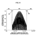
- Fig. 8 shows an electric field intensity distribution of the periodic resonant waveguide mode 701 in the laminating direction.
- Areas 801, 802, 803, 804, and 805 respectively correspond to the Si substrate portion, the multilayer film, an air portion, the lower cladding, and the upper cladding. Since the upper cladding and the lower cladding have a sufficient thickness of 20 nanometer, the periodic resonant waveguide mode is strongly confined in the core area. Therefore, it is found that there is no leakage into the Si substrate portion and the air portion.
- Fig. 9 shows a form of an X-ray waveguide of a second embodiment of the present invention.
- the X-ray waveguide of the second embodiment is formed by a sputtering method in the same manner as in the first embodiment.
- a lower cladding 901 made of tungsten (W) having a thickness of 20 nanometer, a multilayer film 903 having a one-dimensional periodic structure to be a core, and an upper cladding 902 made of tungsten (W) having a thickness of 4 nanometer are formed.
- the multilayer film 903 has a periodic structure in which a film made of carbon (C) having a thickness of 14.4 nanometer and a film made of aluminum oxide (Al 2 O 3 ) having a thickness of 3.6 nanometer are alternately laminated.
- the number of the periods is 25 and the period is 18 nanometer.
- the uppermost portion and the lowermost portion of the core is made of a film of aluminum oxide (Al 2 O 3 ) having a low real part of refractive index.
- the critical angle for total reflection at the interface between the cladding and the core for an X-ray having a photon energy of 8 kilo-electron-volt is about 0.51°.
- the critical angle for total reflection at the interface between the aluminum oxide and the carbon that form the periodic structure in the multilayer film is about 0.19°.
- the Bragg angle due to the periodicity of the multilayer film is about 0.25°. Therefore, the configuration satisfies the formulas (4) and (6).
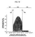
- Fig. 10 shows an electric field intensity distribution in the laminating direction of the periodic resonant waveguide mode 701 that can be present in the X-ray waveguide of the present embodiment.
- Areas 1001, 1002, 1003, 1004, and 1005 respectively correspond to the Si substrate portion, the multilayer film, an air portion, the lower cladding, and the upper cladding.
- Fig. 10 is a calculation result when the photon energy of the X-ray is 8 kilo-electron-volt. The calculation is performed assuming that the air area is a finite space for convenience of calculation.
- the upper cladding 902 Since the upper cladding 902 has a small thickness of 4 nanometer in the present embodiment, light leaks into the air portion 1003 in Fig. 10 . Therefore, by inputting X-rays into the upper cladding at the effective propagation angle of the waveguide mode or at an angle near the effective propagation angle from the outside (air), the X-rays can be introduced into the core from the surface of the upper cladding 902 with evanescent wave coupling. Thereby X-rays can be guided by exciting only a specific periodic resonant waveguide mode.
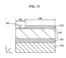
- Fig. 11 shows a form of an X-ray waveguide of a third embodiment of the present invention.
- a lower cladding 1101 made of tungsten (W) having a thickness of 20 nanometer is formed by a sputtering method.
- a multilayer film 1103 having a one-dimensional periodic structure to be a core and an upper cladding 1102 made of tungsten (W) are formed.
- the upper cladding 1102 is formed to have a two-step thickness along the guiding direction of X-rays.
- the thickness of the upper cladding is 1.5 nanometer in the area 1105 and 20 nanometer in the area 1106.
- a part of X-rays 1107 incident onto the surface of the upper cladding 1102 in the area 1105 at a specific angle is coupled to the periodic resonant waveguide mode in the multilayer film 1103, and the periodic resonant waveguide mode is excited in the core to guide the X-rays.
- the length of the area 1105 is about 3 mm in the z direction.
- the incident X-rays are coupled to the waveguide mode in the core, and X-rays of the waveguide mode in the core gradually leak to the outside of the upper cladding 1102.
- the excited periodic resonant waveguide mode is completely confined in the core by the upper cladding having a sufficient thickness in the area 1106. Thereby it is possible to cause the periodic resonant waveguide mode to contribute to the propagation without leaking the X-ray of periodic resonant waveguide mode to the outside of the upper cladding 1102.
- the multilayer film 1103, which is the core, is a multilayer film having a one-dimensional periodic structure in which a film made of boron carbide (B 4 C) having a thickness of 12 nanometer and a film made of aluminum oxide (Al 2 O 3 ) having a thickness of 3 nanometer are alternately laminated. Films forming the upper end portion and the lower end portion of the multilayer film are made of boron carbide (B 4 C) having a high real part of refractive index. The number of the periods is 100 and the period is 15 nanometer.
- the effective propagation angle of the periodic resonant waveguide mode excited in the X-ray waveguide of the present embodiment is about 0.3°.
- the critical angle for total reflection at the interface between the cladding and the core for an X-ray having a photon energy of 10 kilo-electron-volt is about 0.39°.
- the critical angle for total reflection at the interface between the aluminum oxide and the boron carbide that form an unit structure in the multilayer film is about 0.09°.
- the Bragg angle due to the periodicity of the multilayer film is about 0.3°. Therefore, the configuration satisfies the formulas (4) and (6).
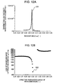
- FIG. 12A shows a result of experiment in which X-rays are incident from a portion where the upper cladding is thin in the X-ray waveguide of the present embodiment while changing the incident angle and X-rays which are guided in the core of the waveguide and outputted X-rays are detected.
- the vertical axis indicates the ratio of the intensity of the guided X-rays to the intensity of the inputted X-rays.
- the incident angle is measured from the surface of the waveguide. When the incident angle substantially corresponds to the effective propagation angle of the waveguide mode, the waveguide mode is excited in the core and X-rays can be guided.
- Fig. 12A is a graph in which the propagation loss of the waveguide mode in the X-ray waveguide of the present embodiment is plotted with the vertical axis representing one obtained by a finite element method using an attenuation constant ⁇ (1/m) and the horizontal axis representing an effective propagation angle of each waveguide mode.
- Fig. 12B is a graph in which the propagation loss of the waveguide mode in the X-ray waveguide of the present embodiment is plotted with the vertical axis representing one obtained by a finite element method using an attenuation constant ⁇ (1/m) and the horizontal axis representing an effective propagation angle of each waveguide mode.
- the point denoted by reference numeral 1202 corresponds to the propagation loss and the effective propagation angle of the periodic resonant waveguide mode, and the fact that this waveguide mode has a propagation loss extremely smaller than that of other waveguide modes matches the experiment.
- the effective propagation angle of the periodic resonant waveguide mode matches the incident angle when the periodic resonant waveguide mode is excited by the experiment, so that it is found that a substantially single waveguide mode with a small loss can be formed by the configuration of the X-ray waveguide of the present invention.
- the X-rays outputted from the X-ray waveguide forms a sharp pattern in a specific direction in far-field region, which means that divergence angle of the outputted X-ray in the far-field region is extremely small.
- the periodic resonant waveguide mode is in phase in near-field region.
- the X-ray waveguide of the present invention can be used in X-ray optical technique field.
- the X-ray waveguide can be used for components employed in an X-ray optical system for operating X-rays outputted from a synchrotron, an X-ray imaging technique, and an X-ray exposure technique.
Landscapes
- Physics & Mathematics (AREA)
- Spectroscopy & Molecular Physics (AREA)
- Engineering & Computer Science (AREA)
- General Engineering & Computer Science (AREA)
- High Energy & Nuclear Physics (AREA)
- Optical Integrated Circuits (AREA)
Applications Claiming Priority (2)
| Application Number | Priority Date | Filing Date | Title |
|---|---|---|---|
| JP2010196522 | 2010-09-02 | ||
| PCT/JP2011/069369 WO2012029676A1 (en) | 2010-09-02 | 2011-08-23 | X-ray waveguide |
Publications (2)
| Publication Number | Publication Date |
|---|---|
| EP2612330A1 EP2612330A1 (en) | 2013-07-10 |
| EP2612330B1 true EP2612330B1 (en) | 2015-03-04 |
Family
ID=44720082
Family Applications (1)
| Application Number | Title | Priority Date | Filing Date |
|---|---|---|---|
| EP20110763785 Not-in-force EP2612330B1 (en) | 2010-09-02 | 2011-08-23 | X-ray waveguide |
Country Status (5)
| Country | Link |
|---|---|
| US (1) | US9129718B2 (enExample) |
| EP (1) | EP2612330B1 (enExample) |
| JP (1) | JP5864945B2 (enExample) |
| CN (1) | CN103081025A (enExample) |
| WO (1) | WO2012029676A1 (enExample) |
Families Citing this family (7)
| Publication number | Priority date | Publication date | Assignee | Title |
|---|---|---|---|---|
| JP5864945B2 (ja) * | 2010-09-02 | 2016-02-17 | キヤノン株式会社 | X線導波路 |
| JP2012226081A (ja) * | 2011-04-19 | 2012-11-15 | Canon Inc | X線導波路 |
| JP2013064713A (ja) * | 2011-08-30 | 2013-04-11 | Canon Inc | X線導波路及びx線導波システム |
| US20130064352A1 (en) * | 2011-09-09 | 2013-03-14 | Canon Kabushiki Kaisha | X-ray waveguide, process of producing x-ray waveguide, and x-ray guiding system |
| JP2013064628A (ja) * | 2011-09-16 | 2013-04-11 | Canon Inc | X線導波路システム |
| US20140294158A1 (en) * | 2013-03-26 | 2014-10-02 | Canon Kabushiki Kaisha | X-ray waveguide |
| CN111048226B (zh) * | 2019-12-27 | 2022-04-26 | 中国科学院长春光学精密机械与物理研究所 | 一种超反射镜 |
Family Cites Families (19)
| Publication number | Priority date | Publication date | Assignee | Title |
|---|---|---|---|---|
| JPH10506756A (ja) * | 1994-10-05 | 1998-06-30 | マサチューセッツ インスティトゥート オブ テクノロジー | 一次元周期誘導体導波路を使用する共振微小空洞 |
| US6847700B1 (en) * | 2001-01-19 | 2005-01-25 | Florida Institute Of Technology | Method and apparatus for delivery of x-ray irradiation |
| JP3857288B2 (ja) * | 2002-07-08 | 2006-12-13 | 日本板硝子株式会社 | フォトニック結晶光導波路 |
| EP1605286A4 (en) * | 2003-03-04 | 2006-04-26 | Nippon Sheet Glass Co Ltd | WAVE LINE DEVICE USING PHOTONIC CRYSTALS |
| US7266284B2 (en) * | 2003-04-17 | 2007-09-04 | University Of Rochester | Method for controlling one or more temperature dependent optical properties of a structure and a system and product thereof |
| JP4875094B2 (ja) * | 2005-10-21 | 2012-02-15 | 01 コミュニーク ラボラトリー インコーポレイテッド | デジタル信号をコンピュータに遠隔的に送信するためのシステム、方法、及びコンピュータプログラム |
| JP2012014152A (ja) * | 2010-06-02 | 2012-01-19 | Canon Inc | X線導波路 |
| JP2012013679A (ja) * | 2010-06-02 | 2012-01-19 | Canon Inc | X線導波路 |
| JP5864892B2 (ja) * | 2010-06-02 | 2016-02-17 | キヤノン株式会社 | X線導波路 |
| JP5864945B2 (ja) * | 2010-09-02 | 2016-02-17 | キヤノン株式会社 | X線導波路 |
| JP2012068125A (ja) * | 2010-09-24 | 2012-04-05 | Canon Inc | X線導波路 |
| JP2012226081A (ja) * | 2011-04-19 | 2012-11-15 | Canon Inc | X線導波路 |
| JP2012237718A (ja) * | 2011-05-13 | 2012-12-06 | Canon Inc | X線ホログラフィ光源素子及びそれを用いたx線ホログラフィシステム |
| JP2013036893A (ja) * | 2011-08-09 | 2013-02-21 | Canon Inc | X線光学系 |
| JP2013064713A (ja) * | 2011-08-30 | 2013-04-11 | Canon Inc | X線導波路及びx線導波システム |
| US20130064352A1 (en) * | 2011-09-09 | 2013-03-14 | Canon Kabushiki Kaisha | X-ray waveguide, process of producing x-ray waveguide, and x-ray guiding system |
| CN103137233A (zh) * | 2011-12-02 | 2013-06-05 | 佳能株式会社 | X射线波导和x射线波导系统 |
| US20130142312A1 (en) * | 2011-12-02 | 2013-06-06 | Canon Kabushiki Kaisha | X-ray waveguide and x-ray waveguide system |
| US20130156162A1 (en) * | 2011-12-02 | 2013-06-20 | Canon Kabushiki Kaisha | X-ray waveguide and x-ray waveguide system |
-
2011
- 2011-08-04 JP JP2011171132A patent/JP5864945B2/ja not_active Expired - Fee Related
- 2011-08-23 US US13/820,072 patent/US9129718B2/en not_active Expired - Fee Related
- 2011-08-23 EP EP20110763785 patent/EP2612330B1/en not_active Not-in-force
- 2011-08-23 WO PCT/JP2011/069369 patent/WO2012029676A1/en not_active Ceased
- 2011-08-23 CN CN2011800412453A patent/CN103081025A/zh active Pending
Also Published As
| Publication number | Publication date |
|---|---|
| US20130163727A1 (en) | 2013-06-27 |
| EP2612330A1 (en) | 2013-07-10 |
| JP5864945B2 (ja) | 2016-02-17 |
| CN103081025A (zh) | 2013-05-01 |
| US9129718B2 (en) | 2015-09-08 |
| WO2012029676A1 (en) | 2012-03-08 |
| JP2012073232A (ja) | 2012-04-12 |
Similar Documents
| Publication | Publication Date | Title |
|---|---|---|
| EP2612330B1 (en) | X-ray waveguide | |
| US8958531B2 (en) | X-ray waveguide | |
| US20130142312A1 (en) | X-ray waveguide and x-ray waveguide system | |
| EP2600355A2 (en) | X-ray waveguide and X-ray waveguide system | |
| US20130156162A1 (en) | X-ray waveguide and x-ray waveguide system | |
| US8559600B2 (en) | X-ray waveguide | |
| JP2012226081A (ja) | X線導波路 | |
| US20130039476A1 (en) | X-ray optical system | |
| Zhu et al. | Engineering the propagation properties of planar plasmonic terahertz waveguides | |
| US20130051534A1 (en) | X-ray waveguide and x-ray waveguide system | |
| US20140294158A1 (en) | X-ray waveguide | |
| EP3460545B1 (en) | Planar waveguide | |
| Prudnikov | X-ray waveguides based on Bragg scattering of multilayers | |
| Belotelov et al. | On surface plasmon polariton wavepacket dynamics in metal–dielectric heterostructures | |
| JP2014215175A (ja) | X線導波路 | |
| JP2013050334A (ja) | エックス線導波路およびその製造方法 | |
| Li | Enhancement of Optical Properties in Artificial Metal-dielectric Structures | |
| Bonnet et al. | Resonant grating effects at terahertz frequencies | |
| US20140056414A1 (en) | X-ray waveguide and x-ray measurement system | |
| Vorgul et al. | Design and optimisation of multimode 1D photonic band gap waveguide | |
| JP2013024630A (ja) | X線光学システム | |
| Shevgaonkar et al. | Propagation characteristics of plasmonic metal stripe waveguide | |
| Smith | Simulations of hybrid long-range plasmon modes with application to 90 bends | |
| JP2013117444A (ja) | X線光学素子及びx線光学システム |
Legal Events
| Date | Code | Title | Description |
|---|---|---|---|
| PUAI | Public reference made under article 153(3) epc to a published international application that has entered the european phase |
Free format text: ORIGINAL CODE: 0009012 |
|
| 17P | Request for examination filed |
Effective date: 20130204 |
|
| AK | Designated contracting states |
Kind code of ref document: A1 Designated state(s): AL AT BE BG CH CY CZ DE DK EE ES FI FR GB GR HR HU IE IS IT LI LT LU LV MC MK MT NL NO PL PT RO RS SE SI SK SM TR |
|
| DAX | Request for extension of the european patent (deleted) | ||
| GRAP | Despatch of communication of intention to grant a patent |
Free format text: ORIGINAL CODE: EPIDOSNIGR1 |
|
| INTG | Intention to grant announced |
Effective date: 20140916 |
|
| GRAS | Grant fee paid |
Free format text: ORIGINAL CODE: EPIDOSNIGR3 |
|
| GRAA | (expected) grant |
Free format text: ORIGINAL CODE: 0009210 |
|
| AK | Designated contracting states |
Kind code of ref document: B1 Designated state(s): AL AT BE BG CH CY CZ DE DK EE ES FI FR GB GR HR HU IE IS IT LI LT LU LV MC MK MT NL NO PL PT RO RS SE SI SK SM TR |
|
| REG | Reference to a national code |
Ref country code: GB Ref legal event code: FG4D |
|
| REG | Reference to a national code |
Ref country code: CH Ref legal event code: EP |
|
| REG | Reference to a national code |
Ref country code: IE Ref legal event code: FG4D |
|
| REG | Reference to a national code |
Ref country code: AT Ref legal event code: REF Ref document number: 714470 Country of ref document: AT Kind code of ref document: T Effective date: 20150415 |
|
| REG | Reference to a national code |
Ref country code: DE Ref legal event code: R096 Ref document number: 602011014401 Country of ref document: DE Effective date: 20150416 |
|
| REG | Reference to a national code |
Ref country code: AT Ref legal event code: MK05 Ref document number: 714470 Country of ref document: AT Kind code of ref document: T Effective date: 20150304 Ref country code: NL Ref legal event code: VDEP Effective date: 20150304 |
|
| PG25 | Lapsed in a contracting state [announced via postgrant information from national office to epo] |
Ref country code: SE Free format text: LAPSE BECAUSE OF FAILURE TO SUBMIT A TRANSLATION OF THE DESCRIPTION OR TO PAY THE FEE WITHIN THE PRESCRIBED TIME-LIMIT Effective date: 20150304 Ref country code: LT Free format text: LAPSE BECAUSE OF FAILURE TO SUBMIT A TRANSLATION OF THE DESCRIPTION OR TO PAY THE FEE WITHIN THE PRESCRIBED TIME-LIMIT Effective date: 20150304 Ref country code: NO Free format text: LAPSE BECAUSE OF FAILURE TO SUBMIT A TRANSLATION OF THE DESCRIPTION OR TO PAY THE FEE WITHIN THE PRESCRIBED TIME-LIMIT Effective date: 20150604 Ref country code: FI Free format text: LAPSE BECAUSE OF FAILURE TO SUBMIT A TRANSLATION OF THE DESCRIPTION OR TO PAY THE FEE WITHIN THE PRESCRIBED TIME-LIMIT Effective date: 20150304 Ref country code: ES Free format text: LAPSE BECAUSE OF FAILURE TO SUBMIT A TRANSLATION OF THE DESCRIPTION OR TO PAY THE FEE WITHIN THE PRESCRIBED TIME-LIMIT Effective date: 20150304 Ref country code: HR Free format text: LAPSE BECAUSE OF FAILURE TO SUBMIT A TRANSLATION OF THE DESCRIPTION OR TO PAY THE FEE WITHIN THE PRESCRIBED TIME-LIMIT Effective date: 20150304 |
|
| REG | Reference to a national code |
Ref country code: LT Ref legal event code: MG4D |
|
| PG25 | Lapsed in a contracting state [announced via postgrant information from national office to epo] |
Ref country code: RS Free format text: LAPSE BECAUSE OF FAILURE TO SUBMIT A TRANSLATION OF THE DESCRIPTION OR TO PAY THE FEE WITHIN THE PRESCRIBED TIME-LIMIT Effective date: 20150304 Ref country code: LV Free format text: LAPSE BECAUSE OF FAILURE TO SUBMIT A TRANSLATION OF THE DESCRIPTION OR TO PAY THE FEE WITHIN THE PRESCRIBED TIME-LIMIT Effective date: 20150304 Ref country code: AT Free format text: LAPSE BECAUSE OF FAILURE TO SUBMIT A TRANSLATION OF THE DESCRIPTION OR TO PAY THE FEE WITHIN THE PRESCRIBED TIME-LIMIT Effective date: 20150304 Ref country code: GR Free format text: LAPSE BECAUSE OF FAILURE TO SUBMIT A TRANSLATION OF THE DESCRIPTION OR TO PAY THE FEE WITHIN THE PRESCRIBED TIME-LIMIT Effective date: 20150605 |
|
| PG25 | Lapsed in a contracting state [announced via postgrant information from national office to epo] |
Ref country code: NL Free format text: LAPSE BECAUSE OF FAILURE TO SUBMIT A TRANSLATION OF THE DESCRIPTION OR TO PAY THE FEE WITHIN THE PRESCRIBED TIME-LIMIT Effective date: 20150304 |
|
| PG25 | Lapsed in a contracting state [announced via postgrant information from national office to epo] |
Ref country code: CZ Free format text: LAPSE BECAUSE OF FAILURE TO SUBMIT A TRANSLATION OF THE DESCRIPTION OR TO PAY THE FEE WITHIN THE PRESCRIBED TIME-LIMIT Effective date: 20150304 Ref country code: RO Free format text: LAPSE BECAUSE OF FAILURE TO SUBMIT A TRANSLATION OF THE DESCRIPTION OR TO PAY THE FEE WITHIN THE PRESCRIBED TIME-LIMIT Effective date: 20150304 Ref country code: SK Free format text: LAPSE BECAUSE OF FAILURE TO SUBMIT A TRANSLATION OF THE DESCRIPTION OR TO PAY THE FEE WITHIN THE PRESCRIBED TIME-LIMIT Effective date: 20150304 Ref country code: PT Free format text: LAPSE BECAUSE OF FAILURE TO SUBMIT A TRANSLATION OF THE DESCRIPTION OR TO PAY THE FEE WITHIN THE PRESCRIBED TIME-LIMIT Effective date: 20150706 Ref country code: EE Free format text: LAPSE BECAUSE OF FAILURE TO SUBMIT A TRANSLATION OF THE DESCRIPTION OR TO PAY THE FEE WITHIN THE PRESCRIBED TIME-LIMIT Effective date: 20150304 |
|
| PG25 | Lapsed in a contracting state [announced via postgrant information from national office to epo] |
Ref country code: IS Free format text: LAPSE BECAUSE OF FAILURE TO SUBMIT A TRANSLATION OF THE DESCRIPTION OR TO PAY THE FEE WITHIN THE PRESCRIBED TIME-LIMIT Effective date: 20150704 Ref country code: PL Free format text: LAPSE BECAUSE OF FAILURE TO SUBMIT A TRANSLATION OF THE DESCRIPTION OR TO PAY THE FEE WITHIN THE PRESCRIBED TIME-LIMIT Effective date: 20150304 |
|
| REG | Reference to a national code |
Ref country code: DE Ref legal event code: R097 Ref document number: 602011014401 Country of ref document: DE |
|
| PG25 | Lapsed in a contracting state [announced via postgrant information from national office to epo] |
Ref country code: IT Free format text: LAPSE BECAUSE OF FAILURE TO SUBMIT A TRANSLATION OF THE DESCRIPTION OR TO PAY THE FEE WITHIN THE PRESCRIBED TIME-LIMIT Effective date: 20150304 |
|
| PLBE | No opposition filed within time limit |
Free format text: ORIGINAL CODE: 0009261 |
|
| STAA | Information on the status of an ep patent application or granted ep patent |
Free format text: STATUS: NO OPPOSITION FILED WITHIN TIME LIMIT |
|
| PG25 | Lapsed in a contracting state [announced via postgrant information from national office to epo] |
Ref country code: DK Free format text: LAPSE BECAUSE OF FAILURE TO SUBMIT A TRANSLATION OF THE DESCRIPTION OR TO PAY THE FEE WITHIN THE PRESCRIBED TIME-LIMIT Effective date: 20150304 |
|
| 26N | No opposition filed |
Effective date: 20151207 |
|
| PG25 | Lapsed in a contracting state [announced via postgrant information from national office to epo] |
Ref country code: SI Free format text: LAPSE BECAUSE OF FAILURE TO SUBMIT A TRANSLATION OF THE DESCRIPTION OR TO PAY THE FEE WITHIN THE PRESCRIBED TIME-LIMIT Effective date: 20150304 |
|
| PG25 | Lapsed in a contracting state [announced via postgrant information from national office to epo] |
Ref country code: LU Free format text: LAPSE BECAUSE OF FAILURE TO SUBMIT A TRANSLATION OF THE DESCRIPTION OR TO PAY THE FEE WITHIN THE PRESCRIBED TIME-LIMIT Effective date: 20150823 Ref country code: MC Free format text: LAPSE BECAUSE OF FAILURE TO SUBMIT A TRANSLATION OF THE DESCRIPTION OR TO PAY THE FEE WITHIN THE PRESCRIBED TIME-LIMIT Effective date: 20150304 |
|
| REG | Reference to a national code |
Ref country code: CH Ref legal event code: PL |
|
| GBPC | Gb: european patent ceased through non-payment of renewal fee |
Effective date: 20150823 |
|
| PG25 | Lapsed in a contracting state [announced via postgrant information from national office to epo] |
Ref country code: CH Free format text: LAPSE BECAUSE OF NON-PAYMENT OF DUE FEES Effective date: 20150831 Ref country code: LI Free format text: LAPSE BECAUSE OF NON-PAYMENT OF DUE FEES Effective date: 20150831 |
|
| REG | Reference to a national code |
Ref country code: IE Ref legal event code: MM4A |
|
| REG | Reference to a national code |
Ref country code: FR Ref legal event code: ST Effective date: 20160429 |
|
| PG25 | Lapsed in a contracting state [announced via postgrant information from national office to epo] |
Ref country code: GB Free format text: LAPSE BECAUSE OF NON-PAYMENT OF DUE FEES Effective date: 20150823 Ref country code: IE Free format text: LAPSE BECAUSE OF NON-PAYMENT OF DUE FEES Effective date: 20150823 |
|
| PG25 | Lapsed in a contracting state [announced via postgrant information from national office to epo] |
Ref country code: FR Free format text: LAPSE BECAUSE OF NON-PAYMENT OF DUE FEES Effective date: 20150831 Ref country code: BE Free format text: LAPSE BECAUSE OF FAILURE TO SUBMIT A TRANSLATION OF THE DESCRIPTION OR TO PAY THE FEE WITHIN THE PRESCRIBED TIME-LIMIT Effective date: 20150304 |
|
| PGFP | Annual fee paid to national office [announced via postgrant information from national office to epo] |
Ref country code: DE Payment date: 20160831 Year of fee payment: 6 |
|
| PG25 | Lapsed in a contracting state [announced via postgrant information from national office to epo] |
Ref country code: MT Free format text: LAPSE BECAUSE OF FAILURE TO SUBMIT A TRANSLATION OF THE DESCRIPTION OR TO PAY THE FEE WITHIN THE PRESCRIBED TIME-LIMIT Effective date: 20150304 |
|
| PG25 | Lapsed in a contracting state [announced via postgrant information from national office to epo] |
Ref country code: SM Free format text: LAPSE BECAUSE OF FAILURE TO SUBMIT A TRANSLATION OF THE DESCRIPTION OR TO PAY THE FEE WITHIN THE PRESCRIBED TIME-LIMIT Effective date: 20150304 Ref country code: HU Free format text: LAPSE BECAUSE OF FAILURE TO SUBMIT A TRANSLATION OF THE DESCRIPTION OR TO PAY THE FEE WITHIN THE PRESCRIBED TIME-LIMIT; INVALID AB INITIO Effective date: 20110823 Ref country code: BG Free format text: LAPSE BECAUSE OF FAILURE TO SUBMIT A TRANSLATION OF THE DESCRIPTION OR TO PAY THE FEE WITHIN THE PRESCRIBED TIME-LIMIT Effective date: 20150304 |
|
| PG25 | Lapsed in a contracting state [announced via postgrant information from national office to epo] |
Ref country code: CY Free format text: LAPSE BECAUSE OF FAILURE TO SUBMIT A TRANSLATION OF THE DESCRIPTION OR TO PAY THE FEE WITHIN THE PRESCRIBED TIME-LIMIT Effective date: 20150304 |
|
| REG | Reference to a national code |
Ref country code: DE Ref legal event code: R119 Ref document number: 602011014401 Country of ref document: DE |
|
| PG25 | Lapsed in a contracting state [announced via postgrant information from national office to epo] |
Ref country code: MK Free format text: LAPSE BECAUSE OF FAILURE TO SUBMIT A TRANSLATION OF THE DESCRIPTION OR TO PAY THE FEE WITHIN THE PRESCRIBED TIME-LIMIT Effective date: 20150304 Ref country code: TR Free format text: LAPSE BECAUSE OF FAILURE TO SUBMIT A TRANSLATION OF THE DESCRIPTION OR TO PAY THE FEE WITHIN THE PRESCRIBED TIME-LIMIT Effective date: 20150304 |
|
| PG25 | Lapsed in a contracting state [announced via postgrant information from national office to epo] |
Ref country code: DE Free format text: LAPSE BECAUSE OF NON-PAYMENT OF DUE FEES Effective date: 20180301 |
|
| PG25 | Lapsed in a contracting state [announced via postgrant information from national office to epo] |
Ref country code: AL Free format text: LAPSE BECAUSE OF FAILURE TO SUBMIT A TRANSLATION OF THE DESCRIPTION OR TO PAY THE FEE WITHIN THE PRESCRIBED TIME-LIMIT Effective date: 20150304 |