EP2611033A2 - Gate driver with digital ground - Google Patents
Gate driver with digital ground Download PDFInfo
- Publication number
- EP2611033A2 EP2611033A2 EP20120195322 EP12195322A EP2611033A2 EP 2611033 A2 EP2611033 A2 EP 2611033A2 EP 20120195322 EP20120195322 EP 20120195322 EP 12195322 A EP12195322 A EP 12195322A EP 2611033 A2 EP2611033 A2 EP 2611033A2
- Authority
- EP
- European Patent Office
- Prior art keywords
- ground
- gate driver
- input buffer
- coupled
- die pad
- Prior art date
- Legal status (The legal status is an assumption and is not a legal conclusion. Google has not performed a legal analysis and makes no representation as to the accuracy of the status listed.)
- Granted
Links
Images



Classifications
-
- H—ELECTRICITY
- H03—ELECTRONIC CIRCUITRY
- H03K—PULSE TECHNIQUE
- H03K19/00—Logic circuits, i.e. having at least two inputs acting on one output; Inverting circuits
- H03K19/003—Modifications for increasing the reliability for protection
- H03K19/00369—Modifications for compensating variations of temperature, supply voltage or other physical parameters
- H03K19/00384—Modifications for compensating variations of temperature, supply voltage or other physical parameters in field effect transistor circuits
-
- H—ELECTRICITY
- H03—ELECTRONIC CIRCUITRY
- H03K—PULSE TECHNIQUE
- H03K17/00—Electronic switching or gating, i.e. not by contact-making and –breaking
- H03K17/14—Modifications for compensating variations of physical values, e.g. of temperature
- H03K17/145—Modifications for compensating variations of physical values, e.g. of temperature in field-effect transistor switches
-
- H—ELECTRICITY
- H03—ELECTRONIC CIRCUITRY
- H03K—PULSE TECHNIQUE
- H03K17/00—Electronic switching or gating, i.e. not by contact-making and –breaking
- H03K17/51—Electronic switching or gating, i.e. not by contact-making and –breaking characterised by the components used
- H03K17/56—Electronic switching or gating, i.e. not by contact-making and –breaking characterised by the components used by the use, as active elements, of semiconductor devices
- H03K17/687—Electronic switching or gating, i.e. not by contact-making and –breaking characterised by the components used by the use, as active elements, of semiconductor devices the devices being field-effect transistors
-
- H—ELECTRICITY
- H10—SEMICONDUCTOR DEVICES; ELECTRIC SOLID-STATE DEVICES NOT OTHERWISE PROVIDED FOR
- H10W—GENERIC PACKAGES, INTERCONNECTIONS, CONNECTORS OR OTHER CONSTRUCTIONAL DETAILS OF DEVICES COVERED BY CLASS H10
- H10W72/00—Interconnections or connectors in packages
-
- H—ELECTRICITY
- H10—SEMICONDUCTOR DEVICES; ELECTRIC SOLID-STATE DEVICES NOT OTHERWISE PROVIDED FOR
- H10W—GENERIC PACKAGES, INTERCONNECTIONS, CONNECTORS OR OTHER CONSTRUCTIONAL DETAILS OF DEVICES COVERED BY CLASS H10
- H10W72/00—Interconnections or connectors in packages
- H10W72/071—Connecting or disconnecting
- H10W72/075—Connecting or disconnecting of bond wires
- H10W72/07551—Connecting or disconnecting of bond wires characterised by changes in properties of the bond wires during the connecting
- H10W72/07554—Connecting or disconnecting of bond wires characterised by changes in properties of the bond wires during the connecting changes in dispositions
-
- H—ELECTRICITY
- H10—SEMICONDUCTOR DEVICES; ELECTRIC SOLID-STATE DEVICES NOT OTHERWISE PROVIDED FOR
- H10W—GENERIC PACKAGES, INTERCONNECTIONS, CONNECTORS OR OTHER CONSTRUCTIONAL DETAILS OF DEVICES COVERED BY CLASS H10
- H10W72/00—Interconnections or connectors in packages
- H10W72/30—Die-attach connectors
- H10W72/321—Structures or relative sizes of die-attach connectors
- H10W72/325—Die-attach connectors having a filler embedded in a matrix
-
- H—ELECTRICITY
- H10—SEMICONDUCTOR DEVICES; ELECTRIC SOLID-STATE DEVICES NOT OTHERWISE PROVIDED FOR
- H10W—GENERIC PACKAGES, INTERCONNECTIONS, CONNECTORS OR OTHER CONSTRUCTIONAL DETAILS OF DEVICES COVERED BY CLASS H10
- H10W72/00—Interconnections or connectors in packages
- H10W72/30—Die-attach connectors
- H10W72/351—Materials of die-attach connectors
- H10W72/352—Materials of die-attach connectors comprising metals or metalloids, e.g. solders
-
- H—ELECTRICITY
- H10—SEMICONDUCTOR DEVICES; ELECTRIC SOLID-STATE DEVICES NOT OTHERWISE PROVIDED FOR
- H10W—GENERIC PACKAGES, INTERCONNECTIONS, CONNECTORS OR OTHER CONSTRUCTIONAL DETAILS OF DEVICES COVERED BY CLASS H10
- H10W72/00—Interconnections or connectors in packages
- H10W72/30—Die-attach connectors
- H10W72/351—Materials of die-attach connectors
- H10W72/353—Materials of die-attach connectors not comprising solid metals or solid metalloids, e.g. ceramics
- H10W72/354—Materials of die-attach connectors not comprising solid metals or solid metalloids, e.g. ceramics comprising polymers
-
- H—ELECTRICITY
- H10—SEMICONDUCTOR DEVICES; ELECTRIC SOLID-STATE DEVICES NOT OTHERWISE PROVIDED FOR
- H10W—GENERIC PACKAGES, INTERCONNECTIONS, CONNECTORS OR OTHER CONSTRUCTIONAL DETAILS OF DEVICES COVERED BY CLASS H10
- H10W72/00—Interconnections or connectors in packages
- H10W72/50—Bond wires
- H10W72/541—Dispositions of bond wires
- H10W72/547—Dispositions of multiple bond wires
-
- H—ELECTRICITY
- H10—SEMICONDUCTOR DEVICES; ELECTRIC SOLID-STATE DEVICES NOT OTHERWISE PROVIDED FOR
- H10W—GENERIC PACKAGES, INTERCONNECTIONS, CONNECTORS OR OTHER CONSTRUCTIONAL DETAILS OF DEVICES COVERED BY CLASS H10
- H10W72/00—Interconnections or connectors in packages
- H10W72/851—Dispositions of multiple connectors or interconnections
- H10W72/874—On different surfaces
- H10W72/884—Die-attach connectors and bond wires
-
- H—ELECTRICITY
- H10—SEMICONDUCTOR DEVICES; ELECTRIC SOLID-STATE DEVICES NOT OTHERWISE PROVIDED FOR
- H10W—GENERIC PACKAGES, INTERCONNECTIONS, CONNECTORS OR OTHER CONSTRUCTIONAL DETAILS OF DEVICES COVERED BY CLASS H10
- H10W74/00—Encapsulations, e.g. protective coatings
-
- H—ELECTRICITY
- H10—SEMICONDUCTOR DEVICES; ELECTRIC SOLID-STATE DEVICES NOT OTHERWISE PROVIDED FOR
- H10W—GENERIC PACKAGES, INTERCONNECTIONS, CONNECTORS OR OTHER CONSTRUCTIONAL DETAILS OF DEVICES COVERED BY CLASS H10
- H10W90/00—Package configurations
- H10W90/701—Package configurations characterised by the relative positions of pads or connectors relative to package parts
- H10W90/731—Package configurations characterised by the relative positions of pads or connectors relative to package parts of die-attach connectors
- H10W90/734—Package configurations characterised by the relative positions of pads or connectors relative to package parts of die-attach connectors between a chip and a stacked insulating package substrate, interposer or RDL
-
- H—ELECTRICITY
- H10—SEMICONDUCTOR DEVICES; ELECTRIC SOLID-STATE DEVICES NOT OTHERWISE PROVIDED FOR
- H10W—GENERIC PACKAGES, INTERCONNECTIONS, CONNECTORS OR OTHER CONSTRUCTIONAL DETAILS OF DEVICES COVERED BY CLASS H10
- H10W90/00—Package configurations
- H10W90/701—Package configurations characterised by the relative positions of pads or connectors relative to package parts
- H10W90/731—Package configurations characterised by the relative positions of pads or connectors relative to package parts of die-attach connectors
- H10W90/736—Package configurations characterised by the relative positions of pads or connectors relative to package parts of die-attach connectors between a chip and a stacked lead frame, conducting package substrate or heat sink
-
- H—ELECTRICITY
- H10—SEMICONDUCTOR DEVICES; ELECTRIC SOLID-STATE DEVICES NOT OTHERWISE PROVIDED FOR
- H10W—GENERIC PACKAGES, INTERCONNECTIONS, CONNECTORS OR OTHER CONSTRUCTIONAL DETAILS OF DEVICES COVERED BY CLASS H10
- H10W90/00—Package configurations
- H10W90/701—Package configurations characterised by the relative positions of pads or connectors relative to package parts
- H10W90/751—Package configurations characterised by the relative positions of pads or connectors relative to package parts of bond wires
- H10W90/754—Package configurations characterised by the relative positions of pads or connectors relative to package parts of bond wires between a chip and a stacked insulating package substrate, interposer or RDL
-
- H—ELECTRICITY
- H10—SEMICONDUCTOR DEVICES; ELECTRIC SOLID-STATE DEVICES NOT OTHERWISE PROVIDED FOR
- H10W—GENERIC PACKAGES, INTERCONNECTIONS, CONNECTORS OR OTHER CONSTRUCTIONAL DETAILS OF DEVICES COVERED BY CLASS H10
- H10W90/00—Package configurations
- H10W90/701—Package configurations characterised by the relative positions of pads or connectors relative to package parts
- H10W90/751—Package configurations characterised by the relative positions of pads or connectors relative to package parts of bond wires
- H10W90/756—Package configurations characterised by the relative positions of pads or connectors relative to package parts of bond wires between a chip and a stacked lead frame, conducting package substrate or heat sink
Definitions
- Various exemplary embodiments disclosed herein relate generally to a gate driver circuit that compensates for parasitic inductances.
- Gate driver circuits may be used to drive gates of power Metal Oxide Semiconductor Field Effect Transistors (MOSFETS) or Insulated Gate Bipolar Transistors (IGBTs).
- MOSFETS Metal Oxide Semiconductor Field Effect Transistors
- IGBTs Insulated Gate Bipolar Transistors
- Gate drivers may be used in two channel devices, also known as dual channel devices. Such devices may drive power devices having both low and high sides.
- a common Integrated Circuit (IC) package, known as SO-8, may use a chip having eight connectors. Such connectors may also be known as pins.
- Another problem may involve instability of the reference voltage for the input side of the gate driver. As this reference is noisy, the input levels may be characterized by unwanted toggling.
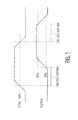
- Fig. 1 illustrates propagation delay definitions for a gate driver circuit.
- Propagation delay, t pd is an important characteristic for gate driver circuits.
- a common definition of propagation delay involves a time difference between the initial time when an input signal rises above the 50% level and the subsequent time when the output signal rises above the 10% level. See t pd (L-LG) on to t pd (H-HG) on .
- a second propagation delay definition involves the time difference between the initial time when the input signal falls below the 50% level and the subsequent time when the output signal falls below the 90% level. See t pd (L-LG) off to t pd (H-HG) off .
- Fig. 2 illustrates an exemplary related art gate driver 200 embodiment that uses input filters 208 / 209.
- Gate driver 200 includes a high input buffer 202, a low input buffer 203, a high undervoltage monitor 204, a low undervoltage monitor 205, a high output driver 206, and a low output driver 207.
- High input filter 208 and low input filter 209 are respectively coupled to the input sides of high input buffer 202 and low input buffer 203.
- Microcontroller 240 includes a high input line 220 coupled to high input filter 208 and a low input line 230 coupled to low input buffer 209.
- the related art embodiment assumes that unwanted voltage excursions only occur for a limited period of time.
- related art devices may add respective input filter 208 / 209 before the input buffers 202 / 203 to prevent propagation of the unwanted voltage excursions.
- this solution has a significant drawback because it adds delay to both the H and L paths.
- Various exemplary embodiments relate to a system for supplying power, the system comprising a gate driver comprising at least one input buffer, at least one undervoltage monitor, at least one output driver, and an exposed die pad, wherein a ground of the at least one input buffer is coupled to the exposed die pad; a microcontroller coupled to the gate driver; a first ground coupled to both the exposed die pad and the microcontroller, wherein the ground compensates for parasitic inductances of the at least one input buffer; and a second ground coupled to a connector of the gate driver.
- a downbond between silicon and the exposed die pad may provide the first ground.
- conductive glue between silicon and the exposed die pad may provide the first ground.
- Various exemplary embodiments further relate to at least one input buffer that may comprise both a high input buffer and a low input buffer. Grounds of both the high input buffer and the low input buffer may be coupled to the first ground.
- the system may have only eight connectors.
- the eight connectors may be H, L, HC, HG, HS, LC, LG, and LS connectors.
- the microcontroller may be coupled to both the H connector and the L connector.
- Various exemplary embodiments further relate to the at least one output driver comprising a high output driver and a low output driver respectively coupled to HG and LG connectors.
- a first transistor may be coupled to the HG connector and a second transistor may be coupled to the LG connector.
- the first ground may be a digital ground and the second ground may be an analog ground.
- Various exemplary embodiments relate to a gate driver, the gate driver comprising at least one input buffer; at least one undervoltage monitor; an exposed die pad that provides a digital ground; at least one output driver, wherein a ground of the at least one input buffer is coupled to the exposed die pad; and an output connector that provides an analog ground.
- a downbond between silicon of the gate driver and the exposed die pad may provide the digital ground.
- conductive glue between silicon of the gate driver and the exposed die pad may provide the digital ground.
- the at least one input buffer may further comprise a high input buffer and a low input buffer. Grounds of both the high input buffer and the low input buffer may be coupled to the digital ground.
- the at least one output driver may further comprise a high output driver and a low output driver.
- the high output driver and the low output driver may be respectively coupled to HG and LG connectors.
- the gate driver may be implemented upon an Integrated Circuit (IC) having only eight connectors.
- the eight connectors may be H, L, HC, HG, HS, LC, LG, and LS connectors.
- Gate driver 300 may include a high input buffer 302, a low input buffer 303, a high undervoltage monitor 304, a low undervoltage monitor 305, a high output driver 306, and a low output driver 307. Both high input buffer 302 and low input buffer 303 may be coupled to ground 310. Ground 310, as described in more detail below, may be an exposed die pad DP. Gate driver may also have eight external connectors. The eight connectors may be H, L, HC, HG, HS, LC, LG, and LS connectors.
- Microcontroller 340 may have a high input line 320 coupled to high input buffer 302 and a low input line 330 coupled to high input buffer 303.
- Microcontroller 340 may be a Digital Signal Processor (DSP).
- a voltage reference of microcontroller 340 may be the same as ground 310.
- Microcontroller 340 may be coupled to both the H connector and the L connector.
- Transistor 360 and transistor 370 may be respectively coupled by their gates to the HG connector and the LG connector.
- ground 310 may not involve an additional connector or pin. Instead, an exposed die pad DP may be used as a ninth connection.
- a connection between the voltage reference of the input buffers 302 / 303 and the voltage reference of the microcontroller 340 may be realized by a bondwire between the input buffer voltage reference and the exposed die pad DP.
- ground 310 may serve as both voltage references.
- Ground 310 may also be considered to be a digital ground.
- PCB Printed Circuit Board
- An LS connector of gate driver 300 may be connected to ground 350, which is separate from ground 310.
- Ground 350 may be considered to be an analog ground or a power ground. Separation of ground 310 from ground 350 may provide various benefits.
- the device may have an additional connection compared to conventional eight-connector packages, the actual connector count may not increase.
- a first advantage involves high immunity to noise transients on the LS connector.
- the voltage reference of the LS connector may be decoupled from the voltage reference of the input buffers 302 / 303.
- a second advantage may involve avoidance of propagation delay.
- a third advantage may involve compliance with common connector and package requirements. Even though there is a ninth connection, the total connector count remains eight. Also, there may be no increase in board space or package costs.
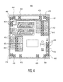
- Fig. 4 illustrates a die plot diagram for the gate driver circuit 300 of Fig. 3 .
- an exemplary test chip 400 may include, in the upper portion of the die plot diagram, HSgateOFF 402, LSgateOFF 403, HSpulseP 404, and LSpulseP 405.
- HSpulseN 406 and LSpulseN 407 may appear respectively, on the left and right sides of the die plot diagram, below HSpulseP 404, and LSpulseP 405.
- the upper half of test chip 400 may include, on its left side, a pair of LC nodes 410. Pairs of LG nodes 412 and LS nodes 414 may appear on its right side.
- pairs of HC nodes 420, HG nodes 422, and HC nodes 424 may be present on its left side. Pairs of L/LSgateON nodes 430 and H/HSgateON nodes 432 may appear on the left side.
- a DATAIN/IrefTest node 440 may appear near the bottom on the left side of test chip 400 while a GND node 450 may appear near the bottom on the right side of test chip 400.
- CLK node 460 may be on the extreme left, near DATAIN node 440.
- Nodes isr_pwrok 470, VBG 480, and vdda1v8 490 then may appear in sequence along the bottom side of test chip 400.
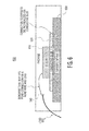
- Fig. 5 illustrates a first embodiment of a die pad connection.
- a PGND connection 500 may include silicon 510, non-conductive glue 520, and an exposed die pad 530.
- a bond wire 540 may couple silicon 510 to a lead 550.
- a downbond 560 may couple silicon 510 to die pad 530.
- Fig. 6 illustrates a second embodiment of a die pad connection. As shown in
- a PGND connection 600 may include silicon 610, conductive glue 620, and an exposed die pad 630.
- a bond wire 640 may couple silicon 610 to a lead 650. No downbond is present.
- conductive glue 620 may provide a connection between die pad 630 and silicon 620.
Landscapes
- Physics & Mathematics (AREA)
- Engineering & Computer Science (AREA)
- Computer Hardware Design (AREA)
- Computing Systems (AREA)
- General Engineering & Computer Science (AREA)
- Mathematical Physics (AREA)
- Semiconductor Integrated Circuits (AREA)
- Electronic Switches (AREA)
- Amplifiers (AREA)
- Power Conversion In General (AREA)
Abstract
Description
- Various exemplary embodiments disclosed herein relate generally to a gate driver circuit that compensates for parasitic inductances.
- Gate driver circuits may be used to drive gates of power Metal Oxide Semiconductor Field Effect Transistors (MOSFETS) or Insulated Gate Bipolar Transistors (IGBTs).
- Gate drivers may be used in two channel devices, also known as dual channel devices. Such devices may drive power devices having both low and high sides. A common Integrated Circuit (IC) package, known as SO-8, may use a chip having eight connectors. Such connectors may also be known as pins.
- Conventional gate drivers may have a problem with parastic inductances on the Printed Circuit Board (PCB). Such parasitic inductances may cause unwanted voltage excursions of the reference voltage both above and below the ground level.
- Another problem may involve instability of the reference voltage for the input side of the gate driver. As this reference is noisy, the input levels may be characterized by unwanted toggling.
-
Fig. 1 illustrates propagation delay definitions for a gate driver circuit. Propagation delay, tpd, is an important characteristic for gate driver circuits. As shown inFig. 1 , a common definition of propagation delay involves a time difference between the initial time when an input signal rises above the 50% level and the subsequent time when the output signal rises above the 10% level. See tpd (L-LG) on to tpd (H-HG) on. A second propagation delay definition involves the time difference between the initial time when the input signal falls below the 50% level and the subsequent time when the output signal falls below the 90% level. See tpd (L-LG) off to tpd (H-HG) off. -
Fig. 2 illustrates an exemplary relatedart gate driver 200 embodiment that usesinput filters 208 / 209.Gate driver 200 includes ahigh input buffer 202, alow input buffer 203, ahigh undervoltage monitor 204, alow undervoltage monitor 205, ahigh output driver 206, and alow output driver 207.High input filter 208 andlow input filter 209 are respectively coupled to the input sides ofhigh input buffer 202 andlow input buffer 203. -
Microcontroller 240 includes ahigh input line 220 coupled tohigh input filter 208 and alow input line 230 coupled tolow input buffer 209. The related art embodiment assumes that unwanted voltage excursions only occur for a limited period of time. Thus, related art devices may addrespective input filter 208 / 209 before theinput buffers 202 / 203 to prevent propagation of the unwanted voltage excursions. However, this solution has a significant drawback because it adds delay to both the H and L paths. Thus, there is a need for an improved gate driver circuit. - A brief summary of various exemplary embodiments is presented. Some simplifications and omissions may be made in the following summary, which is intended to highlight and introduce some aspects of the various exemplary embodiments, but not to limit the scope of the invention. Detailed descriptions of a preferred exemplary embodiment adequate to allow those of ordinary skill in the art to make and use the inventive concepts will follow in later sections.
- Various exemplary embodiments relate to a system for supplying power, the system comprising a gate driver comprising at least one input buffer, at least one undervoltage monitor, at least one output driver, and an exposed die pad, wherein a ground of the at least one input buffer is coupled to the exposed die pad; a microcontroller coupled to the gate driver; a first ground coupled to both the exposed die pad and the microcontroller, wherein the ground compensates for parasitic inductances of the at least one input buffer; and a second ground coupled to a connector of the gate driver.
- In some embodiments, a downbond between silicon and the exposed die pad may provide the first ground. In other embodiments, conductive glue between silicon and the exposed die pad may provide the first ground.
- Various exemplary embodiments further relate to at least one input buffer that may comprise both a high input buffer and a low input buffer. Grounds of both the high input buffer and the low input buffer may be coupled to the first ground.
- In various exemplary embodiments, the system may have only eight connectors. The eight connectors may be H, L, HC, HG, HS, LC, LG, and LS connectors. The microcontroller may be coupled to both the H connector and the L connector.
- Various exemplary embodiments further relate to the at least one output driver comprising a high output driver and a low output driver respectively coupled to HG and LG connectors. A first transistor may be coupled to the HG connector and a second transistor may be coupled to the LG connector.
- In some embodiments, the first ground may be a digital ground and the second ground may be an analog ground.
- Various exemplary embodiments relate to a gate driver, the gate driver comprising at least one input buffer; at least one undervoltage monitor; an exposed die pad that provides a digital ground; at least one output driver, wherein a ground of the at least one input buffer is coupled to the exposed die pad; and an output connector that provides an analog ground.
- In some embodiments, a downbond between silicon of the gate driver and the exposed die pad may provide the digital ground. In other embodiments, conductive glue between silicon of the gate driver and the exposed die pad may provide the digital ground.
- In various exemplary embodiments, the at least one input buffer may further comprise a high input buffer and a low input buffer. Grounds of both the high input buffer and the low input buffer may be coupled to the digital ground.
- In various exemplary embodiments, the at least one output driver may further comprise a high output driver and a low output driver. The high output driver and the low output driver may be respectively coupled to HG and LG connectors.
- In various exemplary embodiments, the gate driver may be implemented upon an Integrated Circuit (IC) having only eight connectors. The eight connectors may be H, L, HC, HG, HS, LC, LG, and LS connectors.
- In order to better understand various exemplary embodiments, reference is made to the accompanying drawings, wherein:
-
Fig. 1 illustrates propagation delay definitions; -
Fig. 2 illustrates a related art gate driver that uses an input filter; -
Fig. 3 illustrates an embodiment of a gate driver; -
Fig. 4 illustrates a die plot diagram for the gate driver ofFig. 3 ; -
Fig. 5 illustrates a first embodiment of a die pad connection; and -
Fig. 6 illustrates a second embodiment of a die pad connection. - Referring now to the drawings, in which like numerals refer to like components or steps, there are disclosed broad aspects of various exemplary embodiments.
- It should be appreciated by those skilled in the art that any block diagrams herein represent conceptual views of illustrative circuitry embodying the principles of the embodiments of the invention.
-
Fig. 3 illustrates an embodiment of a gate driver 300. Gate driver 300 may include ahigh input buffer 302, alow input buffer 303, ahigh undervoltage monitor 304, alow undervoltage monitor 305, ahigh output driver 306, and alow output driver 307. Bothhigh input buffer 302 andlow input buffer 303 may be coupled toground 310.Ground 310, as described in more detail below, may be an exposed die pad DP. Gate driver may also have eight external connectors. The eight connectors may be H, L, HC, HG, HS, LC, LG, and LS connectors. -
Microcontroller 340 may have ahigh input line 320 coupled tohigh input buffer 302 and alow input line 330 coupled tohigh input buffer 303.Microcontroller 340 may be a Digital Signal Processor (DSP). A voltage reference ofmicrocontroller 340 may be the same asground 310.Microcontroller 340 may be coupled to both the H connector and the L connector.Transistor 360 andtransistor 370 may be respectively coupled by their gates to the HG connector and the LG connector. - As depicted in
Fig. 3 ,ground 310 may not involve an additional connector or pin. Instead, an exposed die pad DP may be used as a ninth connection. - In an exemplary embodiment, a connection between the voltage reference of the input buffers 302 / 303 and the voltage reference of the
microcontroller 340 may be realized by a bondwire between the input buffer voltage reference and the exposed die pad DP. Thus,ground 310 may serve as both voltage references.Ground 310 may also be considered to be a digital ground. - There also may be a connection on the Printed Circuit Board (PCB) between the exposed die pad and the voltage reference of the
microcontroller 340. - An LS connector of gate driver 300 may be connected to
ground 350, which is separate fromground 310.Ground 350 may be considered to be an analog ground or a power ground. Separation ofground 310 fromground 350 may provide various benefits. - While the device may have an additional connection compared to conventional eight-connector packages, the actual connector count may not increase.
- A first advantage involves high immunity to noise transients on the LS connector. The voltage reference of the LS connector may be decoupled from the voltage reference of the input buffers 302 / 303. A second advantage may involve avoidance of propagation delay. A third advantage may involve compliance with common connector and package requirements. Even though there is a ninth connection, the total connector count remains eight. Also, there may be no increase in board space or package costs.
-
Fig. 4 illustrates a die plot diagram for the gate driver circuit 300 ofFig. 3 . - As depicted in
Fig. 4 , anexemplary test chip 400 may include, in the upper portion of the die plot diagram,HSgateOFF 402,LSgateOFF 403,HSpulseP 404, andLSpulseP 405.HSpulseN 406 andLSpulseN 407 may appear respectively, on the left and right sides of the die plot diagram, belowHSpulseP 404, andLSpulseP 405. - The upper half of
test chip 400 may include, on its left side, a pair ofLC nodes 410. Pairs ofLG nodes 412 andLS nodes 414 may appear on its right side. - Continuing to the lower half of
test chip 400, pairs ofHC nodes 420,HG nodes 422, andHC nodes 424 may be present on its left side. Pairs of L/LSgateON nodes 430 and H/HSgateON nodes 432 may appear on the left side. A DATAIN/IrefTest node 440 may appear near the bottom on the left side oftest chip 400 while aGND node 450 may appear near the bottom on the right side oftest chip 400. - Four nodes may appear along the bottom side of
test chip 400.CLK node 460 may be on the extreme left, nearDATAIN node 440. Nodes isr_pwrok 470,VBG 480, andvdda1v8 490 then may appear in sequence along the bottom side oftest chip 400. -
Fig. 5 illustrates a first embodiment of a die pad connection. As shown inFig. 5 , aPGND connection 500 may includesilicon 510,non-conductive glue 520, and an exposeddie pad 530. Abond wire 540 may couplesilicon 510 to alead 550. Conversely, adownbond 560 may couplesilicon 510 to diepad 530. -
Fig. 6 illustrates a second embodiment of a die pad connection. As shown in -
Fig. 6 , aPGND connection 600 may includesilicon 610,conductive glue 620, and an exposeddie pad 630. Abond wire 640 may couplesilicon 610 to alead 650. No downbond is present. In the second embodiment,conductive glue 620 may provide a connection betweendie pad 630 andsilicon 620. - Although the various exemplary embodiments have been described in detail with particular reference to certain exemplary aspects thereof, it should be understood that the invention is capable of other embodiments and its details are capable of modifications in various obvious respects. As is readily apparent to those skilled in the art, variations and modifications can be made while remaining within the spirit and scope of the invention. Accordingly, the preceding disclosure, description, and figures are for illustrative purposes only and do not in any way limit the invention, which is defined only by the claims.
Claims (20)
- A system for supplying power, the system comprising:a gate driver comprising at least one input buffer, at least one undervoltage monitor, at least one output driver, and an exposed die pad, wherein a ground of the at least one input buffer is coupled to the exposed die pad;a microcontroller coupled to the gate driver;a first ground coupled to both the exposed die pad and the microcontroller, wherein the ground compensates for parasitic inductances of the at least one input buffer; anda second ground coupled to a connector of the gate driver.
- The system of claim 1, further comprising:a downbond between silicon and the exposed die pad that provides the first ground.
- The system of claim 1, further comprising:conductive glue between silicon and the exposed die pad that provides the first ground.
- The system of claim 1, wherein the at least one input buffer comprises both a high input buffer and a low input buffer.
- The system of claim 4, wherein grounds of both the high input buffer and the low input buffer are coupled to the first ground.
- The system of claim 1, wherein the system has only eight connectors.
- The system of claim 6, wherein the eight connectors are H, L, HC, HG, HS, LC, LG, and LS connectors.
- The system of claim 7, wherein the microcontroller is coupled to both the H connector and the L connector.
- The system of claim 1, wherein the at least one output driver further comprises:a high output driver and a low output driver respectively coupled to HG and LG connectors.
- The system of claim 9, further comprising:a first transistor coupled to the HG connector; anda second transistor coupled to the LG connector.
- The system of claim 1, wherein the first ground is a digital ground and the second ground is an analog ground.
- A gate driver comprising:at least one input buffer;at least one undervoltage monitor;an exposed die pad that provides a digital ground;at least one output driver, wherein a ground of the at least one input buffer is coupled to the exposed die pad; andan output connector that provides an analog ground.
- The gate driver of claim 12, wherein a downbond between silicon of the gate driver and the exposed die pad provides the digital ground.
- The gate driver of claim 12, wherein conductive glue between silicon of the gate driver and the exposed die pad provides the digital ground.
- The gate driver of claim 12, wherein the at least one input buffer further comprises:a high input buffer; anda low input buffer.
- The gate driver of claim 15, wherein grounds of both the high input buffer and the low input buffer are coupled to the digital ground.
- The gate driver of claim 12, wherein the at least one output driver further comprises:a high output driver; anda low output driver.
- The gate driver of claim 17, wherein the high output driver and the low output driver are respectively coupled to HG and LG connectors.
- The gate driver of claim 12, wherein the gate driver is implemented upon an Integrated Circuit (IC) having only eight connectors.
- The gate driver of claim 19, wherein the eight connectors are H, L, HC, HG, HS, LC, LG, and LS connectors.
Applications Claiming Priority (1)
| Application Number | Priority Date | Filing Date | Title |
|---|---|---|---|
| US13/339,433 US8570075B2 (en) | 2011-12-29 | 2011-12-29 | Gate driver with digital ground |
Publications (3)
| Publication Number | Publication Date |
|---|---|
| EP2611033A2 true EP2611033A2 (en) | 2013-07-03 |
| EP2611033A3 EP2611033A3 (en) | 2014-12-24 |
| EP2611033B1 EP2611033B1 (en) | 2019-03-27 |
Family
ID=47471515
Family Applications (1)
| Application Number | Title | Priority Date | Filing Date |
|---|---|---|---|
| EP12195322.8A Not-in-force EP2611033B1 (en) | 2011-12-29 | 2012-12-03 | Gate driver with digital ground |
Country Status (3)
| Country | Link |
|---|---|
| US (1) | US8570075B2 (en) |
| EP (1) | EP2611033B1 (en) |
| CN (1) | CN103187965B (en) |
Families Citing this family (4)
| Publication number | Priority date | Publication date | Assignee | Title |
|---|---|---|---|---|
| US11095284B2 (en) * | 2017-04-21 | 2021-08-17 | Ford Global Technologies, Llc | Minimizing ringing in wide band gap semiconductor devices |
| US10498212B2 (en) * | 2017-05-26 | 2019-12-03 | Dialog Semiconductor (Uk) Limited | Gate driver |
| US10355674B2 (en) * | 2017-07-24 | 2019-07-16 | Arm Limited | Clock gating circuit |
| US10164618B1 (en) * | 2017-12-28 | 2018-12-25 | Micron Technology, Inc. | Jitter cancellation with automatic performance adjustment |
Family Cites Families (15)
| Publication number | Priority date | Publication date | Assignee | Title |
|---|---|---|---|---|
| US5274274A (en) * | 1992-03-23 | 1993-12-28 | Power Integrations, Inc. | Dual threshold differential discriminator |
| US6847103B1 (en) * | 1999-11-09 | 2005-01-25 | Amkor Technology, Inc. | Semiconductor package with exposed die pad and body-locking leadframe |
| US6657399B2 (en) * | 2001-01-26 | 2003-12-02 | International Rectifier Corporation | Self-oscillating circuit for driving high-side and low-side switching devices with variable width pulses |
| WO2002063765A2 (en) * | 2001-02-06 | 2002-08-15 | Koninklijke Philips Electronics N.V. | Integrated fet and driver |
| EP3716257B1 (en) * | 2001-09-07 | 2021-01-20 | Joled Inc. | El display panel, method of driving the same, and el display device |
| US6819011B2 (en) * | 2002-11-14 | 2004-11-16 | Fyre Storm, Inc. | Switching power converter controller with watchdog timer |
| US20040251532A1 (en) * | 2003-06-10 | 2004-12-16 | Potter Chien | Chip package structure |
| US7214985B2 (en) * | 2004-08-23 | 2007-05-08 | Enpirion, Inc. | Integrated circuit incorporating higher voltage devices and low voltage devices therein |
| JP4739059B2 (en) | 2006-02-23 | 2011-08-03 | ルネサスエレクトロニクス株式会社 | Semiconductor device for DC / DC converter |
| DE102007036728B3 (en) | 2007-08-03 | 2008-09-11 | Semikron Elektronik Gmbh & Co. Kg | Driver circuit has two outlets for controlling power semiconductor switch switched-on by signal of voltage against ground potential |
| US20090097291A1 (en) * | 2007-08-16 | 2009-04-16 | Bormann Ronald M | Universal power supply for a laptop |
| US20090057869A1 (en) | 2007-08-31 | 2009-03-05 | Alpha & Omega Semiconductor, Ltd. | Co-packaged high-side and low-side nmosfets for efficient dc-dc power conversion |
| JP4627773B2 (en) * | 2007-10-16 | 2011-02-09 | Okiセミコンダクタ株式会社 | Drive circuit device |
| US20090261462A1 (en) | 2008-04-16 | 2009-10-22 | Jocel Gomez | Semiconductor package with stacked die assembly |
| EP2216905B1 (en) | 2009-02-05 | 2012-08-29 | Abb Oy | Method of controlling an IGBT and a gate driver |
-
2011
- 2011-12-29 US US13/339,433 patent/US8570075B2/en not_active Expired - Fee Related
-
2012
- 2012-11-22 CN CN201210478559.6A patent/CN103187965B/en not_active Expired - Fee Related
- 2012-12-03 EP EP12195322.8A patent/EP2611033B1/en not_active Not-in-force
Non-Patent Citations (1)
| Title |
|---|
| None |
Also Published As
| Publication number | Publication date |
|---|---|
| CN103187965A (en) | 2013-07-03 |
| CN103187965B (en) | 2017-10-20 |
| US8570075B2 (en) | 2013-10-29 |
| EP2611033A3 (en) | 2014-12-24 |
| EP2611033B1 (en) | 2019-03-27 |
| US20130169320A1 (en) | 2013-07-04 |
Similar Documents
| Publication | Publication Date | Title |
|---|---|---|
| US11348914B2 (en) | Semiconductor device | |
| KR102178865B1 (en) | Switch circuit of cascode type having high speed switching performance | |
| US8570075B2 (en) | Gate driver with digital ground | |
| US7012451B2 (en) | Slew rate at buffers by isolating predriver from driver | |
| US7737553B2 (en) | Semiconductor device | |
| TWI492554B (en) | Signal transmission system and signal transmission circuit | |
| US20110157852A1 (en) | Semiconductor device and circuit board | |
| US20050104649A1 (en) | Semiconductor device | |
| US6153914A (en) | Output circuit for integrated circuits | |
| WO2016185847A1 (en) | Input/output interface circuit | |
| US20080217750A1 (en) | Semiconductor device | |
| CN104901659B (en) | Device and integrated circuit for performing signal driving by means of MOSFET | |
| US9070700B2 (en) | Apparatus for electrostatic discharge protection and noise suppression in circuits | |
| CN119921554B (en) | Silicon carbide power device parallel drive oscillation suppression circuit and control method | |
| US11616495B2 (en) | Input circuitry for inter-integrated circuit system | |
| KR101211683B1 (en) | Semiconductor integrated circuit | |
| US6184749B1 (en) | Layout for pull-up/pull-down devices of off-chip driver | |
| JP2001077230A (en) | Lead frame and semiconductor device package using the same | |
| KR101053539B1 (en) | Data output circuit with output driver | |
| JP3409309B2 (en) | Thin film semiconductor integrated circuit | |
| US6642755B2 (en) | Bus driver having noise removing circuit formed by pull-up resistor | |
| KR19980083401A (en) | The input / output buffer of the semiconductor device | |
| US20100007374A1 (en) | On-die thevenin termination for high speed i/o interface | |
| US20070011640A1 (en) | LSI circuit | |
| JP2734427B2 (en) | Output circuit |
Legal Events
| Date | Code | Title | Description |
|---|---|---|---|
| PUAI | Public reference made under article 153(3) epc to a published international application that has entered the european phase |
Free format text: ORIGINAL CODE: 0009012 |
|
| AK | Designated contracting states |
Kind code of ref document: A2 Designated state(s): AL AT BE BG CH CY CZ DE DK EE ES FI FR GB GR HR HU IE IS IT LI LT LU LV MC MK MT NL NO PL PT RO RS SE SI SK SM TR |
|
| AX | Request for extension of the european patent |
Extension state: BA ME |
|
| 17P | Request for examination filed |
Effective date: 20131031 |
|
| RIC1 | Information provided on ipc code assigned before grant |
Ipc: H03K 19/003 20060101ALI20140725BHEP Ipc: H01L 23/00 20060101ALI20140725BHEP Ipc: H03K 17/14 20060101ALI20140725BHEP Ipc: H03K 17/687 20060101AFI20140725BHEP |
|
| PUAL | Search report despatched |
Free format text: ORIGINAL CODE: 0009013 |
|
| AK | Designated contracting states |
Kind code of ref document: A3 Designated state(s): AL AT BE BG CH CY CZ DE DK EE ES FI FR GB GR HR HU IE IS IT LI LT LU LV MC MK MT NL NO PL PT RO RS SE SI SK SM TR |
|
| AX | Request for extension of the european patent |
Extension state: BA ME |
|
| RIC1 | Information provided on ipc code assigned before grant |
Ipc: H03K 19/003 20060101ALI20141117BHEP Ipc: H03K 17/687 20060101AFI20141117BHEP Ipc: H03K 17/14 20060101ALI20141117BHEP Ipc: H01L 23/00 20060101ALI20141117BHEP |
|
| RBV | Designated contracting states (corrected) |
Designated state(s): AL AT BE BG CH CY CZ DE DK EE ES FI FR GB GR HR HU IE IS IT LI LT LU LV MC MK MT NL NO PL PT RO RS SE SI SK SM TR |
|
| STAA | Information on the status of an ep patent application or granted ep patent |
Free format text: STATUS: EXAMINATION IS IN PROGRESS |
|
| 17Q | First examination report despatched |
Effective date: 20170203 |
|
| GRAP | Despatch of communication of intention to grant a patent |
Free format text: ORIGINAL CODE: EPIDOSNIGR1 |
|
| STAA | Information on the status of an ep patent application or granted ep patent |
Free format text: STATUS: GRANT OF PATENT IS INTENDED |
|
| GRAJ | Information related to disapproval of communication of intention to grant by the applicant or resumption of examination proceedings by the epo deleted |
Free format text: ORIGINAL CODE: EPIDOSDIGR1 |
|
| STAA | Information on the status of an ep patent application or granted ep patent |
Free format text: STATUS: EXAMINATION IS IN PROGRESS |
|
| INTG | Intention to grant announced |
Effective date: 20181026 |
|
| GRAP | Despatch of communication of intention to grant a patent |
Free format text: ORIGINAL CODE: EPIDOSNIGR1 |
|
| STAA | Information on the status of an ep patent application or granted ep patent |
Free format text: STATUS: GRANT OF PATENT IS INTENDED |
|
| INTC | Intention to grant announced (deleted) | ||
| INTG | Intention to grant announced |
Effective date: 20181212 |
|
| GRAS | Grant fee paid |
Free format text: ORIGINAL CODE: EPIDOSNIGR3 |
|
| GRAA | (expected) grant |
Free format text: ORIGINAL CODE: 0009210 |
|
| STAA | Information on the status of an ep patent application or granted ep patent |
Free format text: STATUS: THE PATENT HAS BEEN GRANTED |
|
| AK | Designated contracting states |
Kind code of ref document: B1 Designated state(s): AL AT BE BG CH CY CZ DE DK EE ES FI FR GB GR HR HU IE IS IT LI LT LU LV MC MK MT NL NO PL PT RO RS SE SI SK SM TR |
|
| REG | Reference to a national code |
Ref country code: GB Ref legal event code: FG4D |
|
| REG | Reference to a national code |
Ref country code: CH Ref legal event code: EP |
|
| REG | Reference to a national code |
Ref country code: AT Ref legal event code: REF Ref document number: 1114237 Country of ref document: AT Kind code of ref document: T Effective date: 20190415 |
|
| REG | Reference to a national code |
Ref country code: IE Ref legal event code: FG4D |
|
| REG | Reference to a national code |
Ref country code: DE Ref legal event code: R096 Ref document number: 602012058232 Country of ref document: DE |
|
| PG25 | Lapsed in a contracting state [announced via postgrant information from national office to epo] |
Ref country code: SE Free format text: LAPSE BECAUSE OF FAILURE TO SUBMIT A TRANSLATION OF THE DESCRIPTION OR TO PAY THE FEE WITHIN THE PRESCRIBED TIME-LIMIT Effective date: 20190327 Ref country code: NO Free format text: LAPSE BECAUSE OF FAILURE TO SUBMIT A TRANSLATION OF THE DESCRIPTION OR TO PAY THE FEE WITHIN THE PRESCRIBED TIME-LIMIT Effective date: 20190627 Ref country code: LT Free format text: LAPSE BECAUSE OF FAILURE TO SUBMIT A TRANSLATION OF THE DESCRIPTION OR TO PAY THE FEE WITHIN THE PRESCRIBED TIME-LIMIT Effective date: 20190327 Ref country code: FI Free format text: LAPSE BECAUSE OF FAILURE TO SUBMIT A TRANSLATION OF THE DESCRIPTION OR TO PAY THE FEE WITHIN THE PRESCRIBED TIME-LIMIT Effective date: 20190327 |
|
| REG | Reference to a national code |
Ref country code: NL Ref legal event code: MP Effective date: 20190327 |
|
| PG25 | Lapsed in a contracting state [announced via postgrant information from national office to epo] |
Ref country code: BG Free format text: LAPSE BECAUSE OF FAILURE TO SUBMIT A TRANSLATION OF THE DESCRIPTION OR TO PAY THE FEE WITHIN THE PRESCRIBED TIME-LIMIT Effective date: 20190627 Ref country code: RS Free format text: LAPSE BECAUSE OF FAILURE TO SUBMIT A TRANSLATION OF THE DESCRIPTION OR TO PAY THE FEE WITHIN THE PRESCRIBED TIME-LIMIT Effective date: 20190327 Ref country code: NL Free format text: LAPSE BECAUSE OF FAILURE TO SUBMIT A TRANSLATION OF THE DESCRIPTION OR TO PAY THE FEE WITHIN THE PRESCRIBED TIME-LIMIT Effective date: 20190327 Ref country code: LV Free format text: LAPSE BECAUSE OF FAILURE TO SUBMIT A TRANSLATION OF THE DESCRIPTION OR TO PAY THE FEE WITHIN THE PRESCRIBED TIME-LIMIT Effective date: 20190327 Ref country code: HR Free format text: LAPSE BECAUSE OF FAILURE TO SUBMIT A TRANSLATION OF THE DESCRIPTION OR TO PAY THE FEE WITHIN THE PRESCRIBED TIME-LIMIT Effective date: 20190327 Ref country code: GR Free format text: LAPSE BECAUSE OF FAILURE TO SUBMIT A TRANSLATION OF THE DESCRIPTION OR TO PAY THE FEE WITHIN THE PRESCRIBED TIME-LIMIT Effective date: 20190628 |
|
| REG | Reference to a national code |
Ref country code: AT Ref legal event code: MK05 Ref document number: 1114237 Country of ref document: AT Kind code of ref document: T Effective date: 20190327 |
|
| PG25 | Lapsed in a contracting state [announced via postgrant information from national office to epo] |
Ref country code: SK Free format text: LAPSE BECAUSE OF FAILURE TO SUBMIT A TRANSLATION OF THE DESCRIPTION OR TO PAY THE FEE WITHIN THE PRESCRIBED TIME-LIMIT Effective date: 20190327 Ref country code: IT Free format text: LAPSE BECAUSE OF FAILURE TO SUBMIT A TRANSLATION OF THE DESCRIPTION OR TO PAY THE FEE WITHIN THE PRESCRIBED TIME-LIMIT Effective date: 20190327 Ref country code: EE Free format text: LAPSE BECAUSE OF FAILURE TO SUBMIT A TRANSLATION OF THE DESCRIPTION OR TO PAY THE FEE WITHIN THE PRESCRIBED TIME-LIMIT Effective date: 20190327 Ref country code: ES Free format text: LAPSE BECAUSE OF FAILURE TO SUBMIT A TRANSLATION OF THE DESCRIPTION OR TO PAY THE FEE WITHIN THE PRESCRIBED TIME-LIMIT Effective date: 20190327 Ref country code: AL Free format text: LAPSE BECAUSE OF FAILURE TO SUBMIT A TRANSLATION OF THE DESCRIPTION OR TO PAY THE FEE WITHIN THE PRESCRIBED TIME-LIMIT Effective date: 20190327 Ref country code: PT Free format text: LAPSE BECAUSE OF FAILURE TO SUBMIT A TRANSLATION OF THE DESCRIPTION OR TO PAY THE FEE WITHIN THE PRESCRIBED TIME-LIMIT Effective date: 20190727 Ref country code: CZ Free format text: LAPSE BECAUSE OF FAILURE TO SUBMIT A TRANSLATION OF THE DESCRIPTION OR TO PAY THE FEE WITHIN THE PRESCRIBED TIME-LIMIT Effective date: 20190327 Ref country code: RO Free format text: LAPSE BECAUSE OF FAILURE TO SUBMIT A TRANSLATION OF THE DESCRIPTION OR TO PAY THE FEE WITHIN THE PRESCRIBED TIME-LIMIT Effective date: 20190327 |
|
| PG25 | Lapsed in a contracting state [announced via postgrant information from national office to epo] |
Ref country code: SM Free format text: LAPSE BECAUSE OF FAILURE TO SUBMIT A TRANSLATION OF THE DESCRIPTION OR TO PAY THE FEE WITHIN THE PRESCRIBED TIME-LIMIT Effective date: 20190327 Ref country code: PL Free format text: LAPSE BECAUSE OF FAILURE TO SUBMIT A TRANSLATION OF THE DESCRIPTION OR TO PAY THE FEE WITHIN THE PRESCRIBED TIME-LIMIT Effective date: 20190327 |
|
| PG25 | Lapsed in a contracting state [announced via postgrant information from national office to epo] |
Ref country code: AT Free format text: LAPSE BECAUSE OF FAILURE TO SUBMIT A TRANSLATION OF THE DESCRIPTION OR TO PAY THE FEE WITHIN THE PRESCRIBED TIME-LIMIT Effective date: 20190327 Ref country code: IS Free format text: LAPSE BECAUSE OF FAILURE TO SUBMIT A TRANSLATION OF THE DESCRIPTION OR TO PAY THE FEE WITHIN THE PRESCRIBED TIME-LIMIT Effective date: 20190727 |
|
| REG | Reference to a national code |
Ref country code: DE Ref legal event code: R097 Ref document number: 602012058232 Country of ref document: DE |
|
| PG25 | Lapsed in a contracting state [announced via postgrant information from national office to epo] |
Ref country code: DK Free format text: LAPSE BECAUSE OF FAILURE TO SUBMIT A TRANSLATION OF THE DESCRIPTION OR TO PAY THE FEE WITHIN THE PRESCRIBED TIME-LIMIT Effective date: 20190327 |
|
| PLBE | No opposition filed within time limit |
Free format text: ORIGINAL CODE: 0009261 |
|
| STAA | Information on the status of an ep patent application or granted ep patent |
Free format text: STATUS: NO OPPOSITION FILED WITHIN TIME LIMIT |
|
| PG25 | Lapsed in a contracting state [announced via postgrant information from national office to epo] |
Ref country code: SI Free format text: LAPSE BECAUSE OF FAILURE TO SUBMIT A TRANSLATION OF THE DESCRIPTION OR TO PAY THE FEE WITHIN THE PRESCRIBED TIME-LIMIT Effective date: 20190327 |
|
| 26N | No opposition filed |
Effective date: 20200103 |
|
| PG25 | Lapsed in a contracting state [announced via postgrant information from national office to epo] |
Ref country code: TR Free format text: LAPSE BECAUSE OF FAILURE TO SUBMIT A TRANSLATION OF THE DESCRIPTION OR TO PAY THE FEE WITHIN THE PRESCRIBED TIME-LIMIT Effective date: 20190327 |
|
| REG | Reference to a national code |
Ref country code: CH Ref legal event code: PL |
|
| REG | Reference to a national code |
Ref country code: BE Ref legal event code: MM Effective date: 20191231 |
|
| PG25 | Lapsed in a contracting state [announced via postgrant information from national office to epo] |
Ref country code: MC Free format text: LAPSE BECAUSE OF FAILURE TO SUBMIT A TRANSLATION OF THE DESCRIPTION OR TO PAY THE FEE WITHIN THE PRESCRIBED TIME-LIMIT Effective date: 20190327 |
|
| GBPC | Gb: european patent ceased through non-payment of renewal fee |
Effective date: 20191203 |
|
| PG25 | Lapsed in a contracting state [announced via postgrant information from national office to epo] |
Ref country code: GB Free format text: LAPSE BECAUSE OF NON-PAYMENT OF DUE FEES Effective date: 20191203 Ref country code: LU Free format text: LAPSE BECAUSE OF NON-PAYMENT OF DUE FEES Effective date: 20191203 Ref country code: IE Free format text: LAPSE BECAUSE OF NON-PAYMENT OF DUE FEES Effective date: 20191203 |
|
| PG25 | Lapsed in a contracting state [announced via postgrant information from national office to epo] |
Ref country code: LI Free format text: LAPSE BECAUSE OF NON-PAYMENT OF DUE FEES Effective date: 20191231 Ref country code: BE Free format text: LAPSE BECAUSE OF NON-PAYMENT OF DUE FEES Effective date: 20191231 Ref country code: CH Free format text: LAPSE BECAUSE OF NON-PAYMENT OF DUE FEES Effective date: 20191231 |
|
| PGFP | Annual fee paid to national office [announced via postgrant information from national office to epo] |
Ref country code: DE Payment date: 20201119 Year of fee payment: 9 Ref country code: FR Payment date: 20201120 Year of fee payment: 9 |
|
| PG25 | Lapsed in a contracting state [announced via postgrant information from national office to epo] |
Ref country code: CY Free format text: LAPSE BECAUSE OF FAILURE TO SUBMIT A TRANSLATION OF THE DESCRIPTION OR TO PAY THE FEE WITHIN THE PRESCRIBED TIME-LIMIT Effective date: 20190327 |
|
| PG25 | Lapsed in a contracting state [announced via postgrant information from national office to epo] |
Ref country code: MT Free format text: LAPSE BECAUSE OF FAILURE TO SUBMIT A TRANSLATION OF THE DESCRIPTION OR TO PAY THE FEE WITHIN THE PRESCRIBED TIME-LIMIT Effective date: 20190327 Ref country code: HU Free format text: LAPSE BECAUSE OF FAILURE TO SUBMIT A TRANSLATION OF THE DESCRIPTION OR TO PAY THE FEE WITHIN THE PRESCRIBED TIME-LIMIT; INVALID AB INITIO Effective date: 20121203 |
|
| PG25 | Lapsed in a contracting state [announced via postgrant information from national office to epo] |
Ref country code: MK Free format text: LAPSE BECAUSE OF FAILURE TO SUBMIT A TRANSLATION OF THE DESCRIPTION OR TO PAY THE FEE WITHIN THE PRESCRIBED TIME-LIMIT Effective date: 20190327 |
|
| REG | Reference to a national code |
Ref country code: DE Ref legal event code: R119 Ref document number: 602012058232 Country of ref document: DE |
|
| PG25 | Lapsed in a contracting state [announced via postgrant information from national office to epo] |
Ref country code: DE Free format text: LAPSE BECAUSE OF NON-PAYMENT OF DUE FEES Effective date: 20220701 |
|
| PG25 | Lapsed in a contracting state [announced via postgrant information from national office to epo] |
Ref country code: FR Free format text: LAPSE BECAUSE OF NON-PAYMENT OF DUE FEES Effective date: 20211231 |