EP2610860A2 - Ultrasound probe and manufacturing method thereof - Google Patents
Ultrasound probe and manufacturing method thereof Download PDFInfo
- Publication number
- EP2610860A2 EP2610860A2 EP12199703.5A EP12199703A EP2610860A2 EP 2610860 A2 EP2610860 A2 EP 2610860A2 EP 12199703 A EP12199703 A EP 12199703A EP 2610860 A2 EP2610860 A2 EP 2610860A2
- Authority
- EP
- European Patent Office
- Prior art keywords
- piezoelectric member
- groove
- grooves
- ground electrode
- array
- Prior art date
- Legal status (The legal status is an assumption and is not a legal conclusion. Google has not performed a legal analysis and makes no representation as to the accuracy of the status listed.)
- Granted
Links
- 238000002604 ultrasonography Methods 0.000 title claims abstract description 50
- 239000000523 sample Substances 0.000 title claims abstract description 39
- 238000004519 manufacturing process Methods 0.000 title claims abstract description 24
- 239000010410 layer Substances 0.000 description 116
- 238000000034 method Methods 0.000 description 15
- 239000000463 material Substances 0.000 description 9
- 238000009434 installation Methods 0.000 description 7
- 238000005266 casting Methods 0.000 description 4
- 239000004020 conductor Substances 0.000 description 4
- 239000004593 Epoxy Substances 0.000 description 3
- BQCADISMDOOEFD-UHFFFAOYSA-N Silver Chemical compound [Ag] BQCADISMDOOEFD-UHFFFAOYSA-N 0.000 description 3
- 239000000853 adhesive Substances 0.000 description 3
- 230000001070 adhesive effect Effects 0.000 description 3
- 230000015572 biosynthetic process Effects 0.000 description 3
- 230000000694 effects Effects 0.000 description 3
- 239000011241 protective layer Substances 0.000 description 3
- 229910052709 silver Inorganic materials 0.000 description 3
- 239000004332 silver Substances 0.000 description 3
- 238000002591 computed tomography Methods 0.000 description 2
- 239000013078 crystal Substances 0.000 description 2
- 230000000593 degrading effect Effects 0.000 description 2
- NKZSPGSOXYXWQA-UHFFFAOYSA-N dioxido(oxo)titanium;lead(2+) Chemical compound [Pb+2].[O-][Ti]([O-])=O NKZSPGSOXYXWQA-UHFFFAOYSA-N 0.000 description 2
- 238000003384 imaging method Methods 0.000 description 2
- 229910052451 lead zirconate titanate Inorganic materials 0.000 description 2
- 230000035945 sensitivity Effects 0.000 description 2
- 239000006104 solid solution Substances 0.000 description 2
- 239000000126 substance Substances 0.000 description 2
- 206010073306 Exposure to radiation Diseases 0.000 description 1
- 230000003187 abdominal effect Effects 0.000 description 1
- 230000000903 blocking effect Effects 0.000 description 1
- 230000017531 blood circulation Effects 0.000 description 1
- 230000000747 cardiac effect Effects 0.000 description 1
- 239000000919 ceramic Substances 0.000 description 1
- 238000006243 chemical reaction Methods 0.000 description 1
- 230000007547 defect Effects 0.000 description 1
- 238000000151 deposition Methods 0.000 description 1
- 238000003745 diagnosis Methods 0.000 description 1
- 239000003814 drug Substances 0.000 description 1
- 239000011521 glass Substances 0.000 description 1
- JQJCSZOEVBFDKO-UHFFFAOYSA-N lead zinc Chemical compound [Zn].[Pb] JQJCSZOEVBFDKO-UHFFFAOYSA-N 0.000 description 1
- HFGPZNIAWCZYJU-UHFFFAOYSA-N lead zirconate titanate Chemical compound [O-2].[O-2].[O-2].[O-2].[O-2].[Ti+4].[Zr+4].[Pb+2] HFGPZNIAWCZYJU-UHFFFAOYSA-N 0.000 description 1
- 238000002595 magnetic resonance imaging Methods 0.000 description 1
- 239000011159 matrix material Substances 0.000 description 1
- 238000009206 nuclear medicine Methods 0.000 description 1
- 210000000056 organ Anatomy 0.000 description 1
- ZBSCCQXBYNSKPV-UHFFFAOYSA-N oxolead;oxomagnesium;2,4,5-trioxa-1$l^{5},3$l^{5}-diniobabicyclo[1.1.1]pentane 1,3-dioxide Chemical compound [Mg]=O.[Pb]=O.[Pb]=O.[Pb]=O.O1[Nb]2(=O)O[Nb]1(=O)O2 ZBSCCQXBYNSKPV-UHFFFAOYSA-N 0.000 description 1
- 239000011347 resin Substances 0.000 description 1
- 229920005989 resin Polymers 0.000 description 1
- 239000002356 single layer Substances 0.000 description 1
- 210000004872 soft tissue Anatomy 0.000 description 1
- 230000005236 sound signal Effects 0.000 description 1
- 238000001228 spectrum Methods 0.000 description 1
- 238000004659 sterilization and disinfection Methods 0.000 description 1
- XLYOFNOQVPJJNP-UHFFFAOYSA-N water Substances O XLYOFNOQVPJJNP-UHFFFAOYSA-N 0.000 description 1
Images


Classifications
-
- G—PHYSICS
- G01—MEASURING; TESTING
- G01N—INVESTIGATING OR ANALYSING MATERIALS BY DETERMINING THEIR CHEMICAL OR PHYSICAL PROPERTIES
- G01N29/00—Investigating or analysing materials by the use of ultrasonic, sonic or infrasonic waves; Visualisation of the interior of objects by transmitting ultrasonic or sonic waves through the object
- G01N29/22—Details, e.g. general constructional or apparatus details
- G01N29/24—Probes
-
- B—PERFORMING OPERATIONS; TRANSPORTING
- B06—GENERATING OR TRANSMITTING MECHANICAL VIBRATIONS IN GENERAL
- B06B—METHODS OR APPARATUS FOR GENERATING OR TRANSMITTING MECHANICAL VIBRATIONS OF INFRASONIC, SONIC, OR ULTRASONIC FREQUENCY, e.g. FOR PERFORMING MECHANICAL WORK IN GENERAL
- B06B1/00—Methods or apparatus for generating mechanical vibrations of infrasonic, sonic, or ultrasonic frequency
- B06B1/02—Methods or apparatus for generating mechanical vibrations of infrasonic, sonic, or ultrasonic frequency making use of electrical energy
- B06B1/06—Methods or apparatus for generating mechanical vibrations of infrasonic, sonic, or ultrasonic frequency making use of electrical energy operating with piezoelectric effect or with electrostriction
- B06B1/0607—Methods or apparatus for generating mechanical vibrations of infrasonic, sonic, or ultrasonic frequency making use of electrical energy operating with piezoelectric effect or with electrostriction using multiple elements
- B06B1/0622—Methods or apparatus for generating mechanical vibrations of infrasonic, sonic, or ultrasonic frequency making use of electrical energy operating with piezoelectric effect or with electrostriction using multiple elements on one surface
- B06B1/0629—Square array
-
- A—HUMAN NECESSITIES
- A61—MEDICAL OR VETERINARY SCIENCE; HYGIENE
- A61B—DIAGNOSIS; SURGERY; IDENTIFICATION
- A61B8/00—Diagnosis using ultrasonic, sonic or infrasonic waves
- A61B8/13—Tomography
- A61B8/14—Echo-tomography
-
- A—HUMAN NECESSITIES
- A61—MEDICAL OR VETERINARY SCIENCE; HYGIENE
- A61B—DIAGNOSIS; SURGERY; IDENTIFICATION
- A61B8/00—Diagnosis using ultrasonic, sonic or infrasonic waves
- A61B8/44—Constructional features of the ultrasonic, sonic or infrasonic diagnostic device
- A61B8/4483—Constructional features of the ultrasonic, sonic or infrasonic diagnostic device characterised by features of the ultrasound transducer
- A61B8/4494—Constructional features of the ultrasonic, sonic or infrasonic diagnostic device characterised by features of the ultrasound transducer characterised by the arrangement of the transducer elements
-
- G—PHYSICS
- G10—MUSICAL INSTRUMENTS; ACOUSTICS
- G10K—SOUND-PRODUCING DEVICES; METHODS OR DEVICES FOR PROTECTING AGAINST, OR FOR DAMPING, NOISE OR OTHER ACOUSTIC WAVES IN GENERAL; ACOUSTICS NOT OTHERWISE PROVIDED FOR
- G10K11/00—Methods or devices for transmitting, conducting or directing sound in general; Methods or devices for protecting against, or for damping, noise or other acoustic waves in general
- G10K11/002—Devices for damping, suppressing, obstructing or conducting sound in acoustic devices
-
- H—ELECTRICITY
- H10—SEMICONDUCTOR DEVICES; ELECTRIC SOLID-STATE DEVICES NOT OTHERWISE PROVIDED FOR
- H10N—ELECTRIC SOLID-STATE DEVICES NOT OTHERWISE PROVIDED FOR
- H10N30/00—Piezoelectric or electrostrictive devices
- H10N30/01—Manufacture or treatment
- H10N30/03—Assembling devices that include piezoelectric or electrostrictive parts
-
- H—ELECTRICITY
- H10—SEMICONDUCTOR DEVICES; ELECTRIC SOLID-STATE DEVICES NOT OTHERWISE PROVIDED FOR
- H10N—ELECTRIC SOLID-STATE DEVICES NOT OTHERWISE PROVIDED FOR
- H10N30/00—Piezoelectric or electrostrictive devices
- H10N30/1071—Piezoelectric or electrostrictive devices with electrical and mechanical input and output, e.g. having combined actuator and sensor parts
-
- H—ELECTRICITY
- H10—SEMICONDUCTOR DEVICES; ELECTRIC SOLID-STATE DEVICES NOT OTHERWISE PROVIDED FOR
- H10N—ELECTRIC SOLID-STATE DEVICES NOT OTHERWISE PROVIDED FOR
- H10N30/00—Piezoelectric or electrostrictive devices
- H10N30/80—Constructional details
-
- B—PERFORMING OPERATIONS; TRANSPORTING
- B06—GENERATING OR TRANSMITTING MECHANICAL VIBRATIONS IN GENERAL
- B06B—METHODS OR APPARATUS FOR GENERATING OR TRANSMITTING MECHANICAL VIBRATIONS OF INFRASONIC, SONIC, OR ULTRASONIC FREQUENCY, e.g. FOR PERFORMING MECHANICAL WORK IN GENERAL
- B06B1/00—Methods or apparatus for generating mechanical vibrations of infrasonic, sonic, or ultrasonic frequency
- B06B1/02—Methods or apparatus for generating mechanical vibrations of infrasonic, sonic, or ultrasonic frequency making use of electrical energy
- B06B1/06—Methods or apparatus for generating mechanical vibrations of infrasonic, sonic, or ultrasonic frequency making use of electrical energy operating with piezoelectric effect or with electrostriction
- B06B1/0607—Methods or apparatus for generating mechanical vibrations of infrasonic, sonic, or ultrasonic frequency making use of electrical energy operating with piezoelectric effect or with electrostriction using multiple elements
- B06B1/0622—Methods or apparatus for generating mechanical vibrations of infrasonic, sonic, or ultrasonic frequency making use of electrical energy operating with piezoelectric effect or with electrostriction using multiple elements on one surface
- B06B1/064—Methods or apparatus for generating mechanical vibrations of infrasonic, sonic, or ultrasonic frequency making use of electrical energy operating with piezoelectric effect or with electrostriction using multiple elements on one surface with multiple active layers
-
- Y—GENERAL TAGGING OF NEW TECHNOLOGICAL DEVELOPMENTS; GENERAL TAGGING OF CROSS-SECTIONAL TECHNOLOGIES SPANNING OVER SEVERAL SECTIONS OF THE IPC; TECHNICAL SUBJECTS COVERED BY FORMER USPC CROSS-REFERENCE ART COLLECTIONS [XRACs] AND DIGESTS
- Y10—TECHNICAL SUBJECTS COVERED BY FORMER USPC
- Y10T—TECHNICAL SUBJECTS COVERED BY FORMER US CLASSIFICATION
- Y10T29/00—Metal working
- Y10T29/42—Piezoelectric device making
Definitions
- Exemplary embodiments of the present disclosure relate to an ultrasound probe for generating images of the inside of a subject using ultrasonic waves.
- An ultrasound diagnostic system includes a noninvasive apparatus that irradiates an ultrasound signal to a body surface at a target organ in the body and obtains cross-sectional images of, for example, soft tissue and blood flow.
- the ultrasound diagnostic system may have a compact size and low price, display images in real time, and provide a high level of safety by eliminating exposure to radiation.
- an ultrasound diagnostic system has been widely used for diagnosis in, for example, cardiac medicine, abdominal imaging, urology, obstetrics and gynecology.
- the ultrasound diagnostic system includes an ultrasound probe which transmits an ultrasound signal to a subject and receives an ultrasound echo signal reflected from the subject to obtain an ultrasound image of the subject.
- the ultrasound probe includes a piezoelectric layer of piezoelectric materials which convert electric signals into sound signals (e.g., acoustic), and vice versa, through vibration of the piezoelectric materials, a matching layer to reduce a difference in acoustic impedance between the piezoelectric layer and the subject to allow ultrasonic waves transmitted from the piezoelectric layer to be transferred to the subject as much as possible, and a lens to focus the ultrasonic waves traveling from the front of the piezoelectric layer on a specific point, and a backing layer to block the ultrasonic waves from traveling in an opposite direction from the rear of the piezoelectric layer to prevent image distortion.
- a piezoelectric layer of piezoelectric materials which convert electric signals into sound signals (e.g., acoustic), and vice versa, through vibration of the piezoelectric materials
- a matching layer to reduce a difference in acoustic impedance between the piezoelectric layer and the subject to allow ultrasonic waves transmitted from the piez
- an ultrasound probe including a backing layer and/or a matching layer provided with grooves in which a piezoelectric member is allowed to be installed, and a manufacturing method thereof.
- an ultrasound probe includes a piezoelectric member, and a backing layer disposed on a rear-side surface of the piezoelectric member and provided, on a front-side surface of the backing layer, with at least one groove in which the piezoelectric member is installed.
- the piezoelectric member may be arranged as one of a one-dimensional array and a two-dimensional array, and the at least one groove may have a shape corresponding to the array of the piezoelectric member.
- a ground electrode may be formed on at least one side of each of elements constituting the array of the piezoelectric member, and a signal electrode may be formed on at least one side of each of the elements including a side opposite to the side on which the ground electrode is formed.
- At least one conductive pattern to apply an electric signal to the array of the piezoelectric member may be installed in the at least one groove.
- the at least one conductive pattern may be formed on at least one side of the at least one groove.
- the at least one conductive pattern may be electrically connected with at least one of a ground electrode and a signal electrode formed on an element of the array of the piezoelectric member to apply an electric signal to the element.
- an ultrasound probe includes a piezoelectric member, and a matching layer disposed on a front-side surface of the piezoelectric member and provided, on a rear-side surface of the matching layer, with at least one groove in which the piezoelectric member is installed.
- the piezoelectric member may be arranged as one of a one-dimensional array and a two-dimensional array, and the at least one groove may have a shape corresponding to the array of the piezoelectric member.
- a ground electrode may be formed on at least one side of each of elements constituting the array of the piezoelectric member, and a signal electrode may be formed on at least one side of each of the elements including a side opposite to the side on which the ground electrode is formed.
- At least one conductive pattern to apply an electric signal to the array of the piezoelectric member may be installed in the at least one groove.
- the at least one conductive pattern may be formed on at least one side of the at least one groove.
- the at least one conductive pattern may be electrically connected with at least one of a ground electrode and a signal electrode formed on an element of the array of the piezoelectric member to apply an electric signal to the element.
- a manufacturing method of an ultrasound probe includes forming at least one groove on one side of a backing layer, and installing a piezoelectric member in the at least one groove.
- the forming at least one groove may include arranging, on the one side of the backing layer, the at least one groove in one of a one-dimensional array and a two-dimensional array, and forming, on at least one side of the at least one groove, at least one conductive pattern to apply an electric signal to the array of the piezoelectric member.
- the installing a piezoelectric member may include installing a matching layer on one side of the piezoelectric member, processing the piezoelectric member on which the matching layer is installed into one of a one-dimensional array and a two-dimensional array, forming a ground electrode and a signal electrode on each of elements constituting the array of the processed piezoelectric member, and installing, in the at least one groove, the array of the piezoelectric member provided with the ground and signal electrodes.
- the forming a ground electrode and a signal electrode may include forming the ground electrode on at least one side of each element constituting the array of the processed piezoelectric member, and forming the signal electrode on at least one side of each element including a side opposite to the side on which the ground electrode is formed.
- At least one conductive pattern may be formed in the at least one groove to be electrically connected with at least one of the ground electrode and the signal electrode to apply an electric signal to the element.
- a manufacturing method of an ultrasound probe includes forming at least one groove on one side of a matching layer, and installing a piezoelectric member in the at least one groove.
- the forming at least one groove may include arranging, on the one side of the matching layer, the at least one groove in one of a one-dimensional array and a two-dimensional array, and forming, on at least one side of the at least one groove, at least one conductive pattern to apply an electric signal to the array of the piezoelectric member.
- the installing a piezoelectric member may include processing the piezoelectric member into one of a one-dimensional array and a two-dimensional array, forming a ground electrode and a signal electrode on each of elements constituting the array of the processed piezoelectric member, and installing, in the at least one groove, the array of the piezoelectric member provided with the ground and signal electrodes.
- the forming a ground electrode and a signal electrode may include forming the ground electrode on at least one side of each element constituting the array of the processed piezoelectric member, and forming the signal electrode on at least one side of each element including a side opposite to the side on which the ground electrode is formed.
- At least one conductive pattern may be formed in the at least one groove to be electrically connected with at least one of the ground electrode and the signal electrode to apply an electric signal to the element.
- an ultrasound probe includes a piezoelectric member including a front-side surface and a rear-side surface, a backing layer disposed on the rear-side surface for absorbing at least a portion of ultrasonic waves generated in the piezoelectric member, and a matching layer disposed on the front-side surface for reducing a difference in acoustic impedance between the piezoelectric member and a subject, wherein at least one of the backing layer and matching layer includes a groove in which the piezoelectric member is installed.
- the backing layer may include the groove.
- the matching layer may include the groove.
- a conductive pattern may be formed in the groove to apply an electric signal to the piezoelectric member.
- An electrode may be formed on a surface of the piezoelectric member and electrically coupled to the conductive pattern.
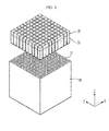
- FIG. 1 is an exploded perspective view illustrating a two-dimensional-array of an ultrasound probe according to an exemplary embodiment of the present disclosure
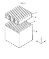
- FIG. 2 is an exploded perspective view illustrating a one-dimensional-array of an ultrasound probe according to an exemplary embodiment of the present disclosure.
- the ultrasound probe according to the exemplary embodiment includes a piezoelectric layer 20, a matching layer 10 disposed on a front-side surface of the piezoelectric layer 20, and a backing layer 30 disposed on a rear-side surface of the piezoelectric layer 20.
- a piezoelectric material generates a voltage in response to applied mechanical stress, and is mechanically deformed in response to an applied voltage. These effects are referred to as a piezoelectric effect and an inverse piezoelectric effect, respectively.
- a piezoelectric material is a material that converts electric energy into mechanical vibration energy, and vice versa.
- the ultrasound probe includes the piezoelectric layer 20 formed of a piezoelectric material(s) that generates an ultrasound by converting an applied electric signal into mechanical vibration.
- Examples of piezoelectric materials constituting the piezoelectric layer 20 may include at least one of lead zirconate titanate (PZT) ceramics, PZMT single crystals made of a solid solution of lead magnesium niobate and lead titanate, PZNT single crystals made of a solid solution of lead zinc niobate and lead titanate, or the like.
- PZT lead zirconate titanate
- the piezoelectric layer 20 may be arranged in either a single layer or a multilayered stack.
- the impedance and voltage of the piezoelectric layer 20 may be adjusted more easily, and better piezoelectric sensitivity, higher energy conversion efficiency and a smoother spectrum may be obtained.
- the matching layer 10 is disposed on the front-side surface of the piezoelectric layer 20.
- the matching layer 10 reduces a difference in acoustic impedance between the piezoelectric layer 20 and the subject to enable matching the acoustic impedance of the piezoelectric layer 20 with that of the subject, thereby allowing ultrasound generated by the piezoelectric layer 20 to be efficiently transferred to the subject.
- the matching layer 10 may be adapted to have a middle value between the acoustic impedances of the piezoelectric layer 20 and the subject.
- the matching layer 10 may be formed of a glass or resin material. Also, a plurality of matching layers 10 may be provided to allow the acoustic impedance to vary gradually from the piezoelectric layer 20 toward the subject, and each of the plurality of matching layers may be formed of a different material.
- the piezoelectric layer 20 and the matching layer 10 may be formed in a dicing process as a two-dimensional array in the shape of a matrix shown in FIG. 1 , or as a one-dimensional array shown in FIG. 2 .
- a protective layer may be disposed on a front-side surface of the matching layer 10.
- the protective layer may prevent high frequency signals generated by the piezoelectric layer 20 from being exposed to the outside and may block introduction of external high frequency signals.
- the protective layer may protect internal components from water and chemicals such as those used for disinfection, by applying or depositing a conductive material to the surface of a film with moisture-resistance and chemical resistance.
- a lens may be disposed on the front-side surface of the matching layer 10.
- the lens may be formed to be convex in a direction of irradiation of the ultrasonic waves to focus the ultrasonic waves, or may be formed to be concave in case the sound velocity is lower than in the subject.
- the backing layer 30, which is disposed on the rear-side surface of the piezoelectric layer 20, absorbs a portion of the ultrasonic waves generated in the piezoelectric layer 20 and traveling in a backward direction. This blocks the portion of the ultrasonic waves from being reflected in a forward direction, thereby preventing image distortion.
- a plurality of backing layers 30 may be provided.
- the backing layer 30 is also formed to have a plurality of grooves 31 arranged in a two-dimensional array, as shown in FIG. 1 .
- the number of grooves 31 may be equal to that of elements21 (see FIG. 4 ) constituting the two-dimensional array of the piezoelectric layer 20, and each of the grooves 31 may be formed to have the same or a similar cross-sectional shape as that of the corresponding element 21 so that the respective elements 21 may be seated in the grooves 31.
- the backing layer 30 is also formed to have a plurality of grooves 31 arranged in a one-dimensional array, as shown in FIG. 2 .
- the number of grooves 31 may be equal to that of elements 21 constituting the one-dimensional array of the piezoelectric layer 20, and each of the grooves 31 may be formed to have the same or a similar cross-sectional shape as that of the corresponding element 21 so that the respective elements 21 may be seated in the grooves 31.
- the depth of the grooves 31 may be set to allow the elements 21 to be stably seated while not degrading the efficiency of generating ultrasonic waves.
- the manufacturing technique used for forming the grooves 31 in the backing layer 30 is not limited. Various manufacturing techniques may be used depending on, for example, the shape of the grooves 31. For instance, in one exemplary process, the backing layer 30 provided with grooves 31 may be manufactured through casting.
- an adhesive When the elements 21 are installed in corresponding grooves 31, an adhesive, a silver epoxy, a conductive material, or the like, may be inserted between contact surfaces of the element 21 and the groove 31 for increasing accuracy in arranging the elements 21 to allow the elements 21 to be securely installed in the grooves 31.
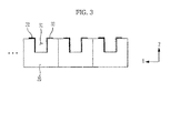
- FIG. 3 illustrates an example of conductive patterns 32 and 33 formed in the grooves 31 of the backing layer 30 of the ultrasound probe according to an exemplary embodiment of the present disclosure
- FIG.'S 4 and 5 illustrate an example of a piezoelectric member which may be installed in the groove 31 in FIG. 3 and installation thereof in the groove 31, respectively
- FIG.'S 6 and 7 illustrate another example of a piezoelectric member which may be installed in the groove 31 in FIG. 3 and installation thereof in the groove 31, respectively.
- the piezoelectric member For the piezoelectric layer 20 to generate ultrasonic waves, an electric signal should be applied to the piezoelectric member constituting the piezoelectric layer 20. Therefore, the piezoelectric member is provided with electrodes 22 and 23, that is, a ground electrode 22 and a signal electrode 23, to which an electric signal is applied.
- the ground electrode 22 and signal electrode 23 are formed on each of the elements 21 constituting the array.
- conductive patterns 32 and 33 are formed in each of the grooves 31 in which the elements 21 are installed.
- the conductive patterns 32 and 33 may be formed to extend from both lateral sides of the groove 31 to outside the groove 31.
- the portions of the conductive patterns 32 and 33 extending outside the groove 31 may be electrically connected to an electric signal-supply member, for example, a printed circuit board (PCB) or a flexible printed circuit board (FPCB).
- PCB printed circuit board
- FPCB flexible printed circuit board
- the conductive patterns 32 and 33 extending toward each other from any two adjacent grooves 31 to the outside thereof may be formed to have different polarities.
- the conductive patterns 32 and 33 extending toward each other from the adjacent grooves 31 to the outside thereof are arranged not to contact each other.
- the conductive patterns 32 and 33 extending toward each other from any two adjacent grooves 31 to the outside thereof have the same polarity, that is, when both conductive patterns 32 and 33 contact the ground electrode 22 or both conductive patterns 32 and 33 contact the signal electrode 23, they may be connected to each other.
- the electric signals applied to the elements 21 need to be adjusted differently from each other, and thus the conductive patterns 32 and 33 formed by extending toward each other from the adjacent grooves 31 to the outside thereof may be provided with different polarities and arranged not to contact each other, as shown in FIG. 3 .
- FIG. 4 shows the piezoelectric member provided with the electrodes 22 and 23 adapted to be installed in the grooves 31.
- the ground electrode 22 and signal electrode 23 may be formed on corresponding opposite lateral side surfaces of the element 21 as shown in FIG. 4 , so that when the element 21 is installed in the groove 31 (see FIG. 5 ), the ground electrode 22 and signal electrode 23 formed on the element 21 may contact the conductive patterns 32 and 33, respectively.
- the ground electrode 22 and signal electrode 23 may be formed only on the opposite lateral side surfaces of the element 21, or may further extend therefrom toward the front-side surface or rear-side surface of the element 21.
- ground electrode 22 and signal electrode 23 may be formed on the front-side and rear-side surfaces of the element 21 rather than on the opposite lateral side surfaces of the element 21 as shown in FIG. 13 .
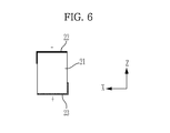
- FIG. 6 shows the ground electrode 22 and signal electrode 23 formed on the front-side and rear-side surfaces of the element 21 and FIG. 7 illustrates installation of the element 21 of FIG. 6 in the groove 31.
- ground electrode 22 and signal electrode 23 When the ground electrode 22 and signal electrode 23 are formed on the front-side and rear-side surfaces of the element 21, they may extend toward opposite lateral side surfaces so that when the element 21 is installed in the groove 31, the ground electrode 22 and signal electrode 23 formed on the front-side and rear-side surfaces of the element 21, respectively, may contact the corresponding conductive patterns 32 and 33.
- FIG. 8 illustrates another example of conductive patterns 32 and 33 formed in the groove 31 of the backing layer 30 of the ultrasound probe according to an exemplary embodiment of the present disclosure
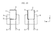
- FIG. 9 shows a piezoelectric member that may be installed in the grooves 31 of FIG. 8
- FIG. 10 illustrates installation of the piezoelectric member of FIG. 9 in the grooves 31 of FIG. 8 .
- a bottom of the groove 31 may be provided with two conductive patterns 32 and 33 which are connected respectively to the ground electrode 22 and signal electrode 23.
- the conductive patterns 32 and 33 may be exposed at the bottom of the groove 31 and extend to a rear side of the backing layer 30 through an internal portion of the backing layer 30. At the rear side of the backing layer 30, the conductive patterns 32 and 33 may be connected to an external member supplying electrical signals.
- FIG. 9 shows the piezoelectric member provided with the ground electrode 22 and signal electrode 23 adapted to be installed in the grooves 31.
- the ground electrode 22 and signal electrode 23 may be formed on the element 21 as shown in FIG. 9 , so that when the element 21 is installed in the groove 31 (see FIG. 10 ), the ground electrode 22 and signal electrode 23 may contact the conductive patterns 32 and 33, respectively.
- the ground electrode 22 and signal electrode 23 are formed on the front-side and rear-side surfaces of the element 21, the ground electrode 22 is arranged on the rear-side surface and the signal electrode 23 on the front-side surface.
- the signal electrode 23 formed on the front-side surface of the element 21 may be arranged to extend to the rear-side surface of the element 21 along a lateral side surface of the element 21.
- the ground electrode 22 may be formed on the front-side surface of the element 21 and the signal electrode 23 formed on the rear-side surface of the element 21 as shown in, for example, FIG. 6 .
- ground electrode 22 and signal electrode 23 are formed on lateral side surfaces of the element 21, the ground electrode 22 and the signal electrode 23 may be respectively arranged on the opposite lateral side surfaces of element 21 and both may be arranged to extend to the rear-side surface of the element 21.
- one of the ground electrode 22 and signal electrode 23 may extend to a surface of the element 21 on which the other one of the ground electrode 22 and signal electrode 23 is formed, as shown in the example on the left in FIG. 9 .
- both the ground electrode 22 and signal electrode 23 may be formed to extend from the lateral side surfaces of the element 21 to the rear-side surface of the element 21 as shown in the example on the right in FIG. 9 , and in this case the conductive patterns 32 and 33 may be provided only at the bottom of the groove 31.
- ground electrode 22 and signal electrode 23 extending to the rear-side surface of the element 21 only need to be connected to the respective conductive patterns 32 and 33 formed on the bottom of the groove 31, they may be arranged to occupy as small an area of the rear-side surface of the element 21 as possible.
- FIG.'S 11 and 12 illustrate further examples of conductive patterns formed in the grooves 31 of the backing layer 30 of an ultrasound probe according to another embodiment of the present disclosure
- FIG. 13 shows a piezoelectric member that may be installed in the grooves 31 of FIG.'S 11 and 12.
- the backing layer 30 shown in FIG. 11 includes a backing member 34 provided with the grooves 31, a backing block 35 to support the backing member 34, and a conductive pattern 32 installed between the backing member 34 and the backing block 35.
- the conductive pattern 32 is electrically connected to an external member supplying electric signals and contacts one of the ground electrode 22 and signal electrode 23 of the element 21.
- conductive patterns 32 and 33 there are not two conductive patterns 32 and 33 formed to contact the ground electrode 22 and signal electrode 23, respectively, like the conductive patterns 32 and 33 in FIG.'S 3 and 8 described above, but one conductive pattern 32 is provided to contact only one of the ground electrode 22 and signal electrode 23.
- the conductive pattern 32 shown in FIG. 12 may be exposed at the bottom of the groove 31 to contact the ground electrode 22 of the element 21 to be installed in the groove 31, and may extend to the rear side of the backing layer 30 through the internal portion (e.g., backing block 35) of the backing layer 30. At the rear side of the backing layer 30, the conductive pattern 32 may be connected to an external member supplying electric signals.
- the conductive pattern 32 in FIG. 12 contacts one of the ground electrode 22 and signal electrode 23 of the element 21.
- FIG. 13 illustrates a piezoelectric member provided with the ground electrode 22 and signal electrode 23 to be installed in the grooves 31 in FIG.'S 11 and 12.
- the ground electrode 22 and signal electrode 23 formed on the element 21 may be arranged on the front-side and rear-side surfaces of the element 21 as shown in FIG. 13 , so that when the element 21 is installed in the groove 31, the one of the ground electrode 22 and signal electrode 23 may contact the conductive pattern 32.
- only the ground electrode 22 formed on the rear-side surface of the element 21 may receive an electric signal from the conductive pattern 32 formed in the groove 31.
- the signal electrode 23 formed on the front-side surface of the element 21 may receive an electric signal from a separate conductive pattern to be installed on the front-side surface of the piezoelectric member.
- the ground electrode 22 and signal electrode 23 may be formed only on the front-side and rear-side surfaces of the element 21, or may be arranged to extend from the front-side and rear-side surfaces to the opposite lateral side surfaces.
- FIG.'S 14 and 15 illustrate another exemplary embodiment of the present disclosure. That is, grooves 11 in which corresponding piezoelectric members are installed are formed in the matching layer 10 rather than in the backing layer 30.
- the matching layer 10 is formed to have a plurality of grooves 11 arranged in a two-dimensional array, as shown in FIG. 14 .
- the number of grooves 11 may be equal to that of the elements 21 constituting the two-dimensional array of the piezoelectric layer 20, and each of the grooves 31 may be formed to have the same or a similar cross-sectional shape as that of the corresponding element 21 so that the respective elements 21 may be installed in the grooves 31.
- the matching layer 10 is formed to have a plurality of grooves 11 arranged in a one-dimensional array, as shown in FIG. 15 .
- the number of grooves 11 may be equal to that of the elements 21 constituting the one-dimensional array of the piezoelectric layer 20, and each of the grooves 31 may be formed to have the same or a similar cross-sectional shape as that of the corresponding element 21 so that the respective elements 21 may be installed in the grooves 31.
- the depth of the grooves 11 may be set to allow the elements 21 to be stably seated while not degrading the efficiency of generating ultrasonic waves.
- the manufacturing technique used for forming the grooves 11 in the matching layer 10 is not limited. Various manufacturing techniques may be used depending on, for example, the shape of the grooves 11. For instance, in one exemplary process, the matching layer 10 provided with grooves 11 may be manufactured through casting.
- the orientation of the ground electrode 22 and signal electrode 23 formed on the elements 21 and the conductive patterns 32 and 33 formed in the grooves 11 are opposite to that defined in the exemplary embodiments illustrated in FIG.'S 3 to 13.
- the other details of the ground electrode 22 and signal electrode 23 and the conductive patterns 32 and 33 are the same as those for the embodiments illustrated in FIG.'S 3 to 13, and thus for the other details, refer to the description given above with respect to FIG.'S 3 to 13.
- FIG. 16 is a flowchart illustrating a manufacturing method of the ultrasound probe according to an exemplary embodiment of the present disclosure.
- the matching layer 10 is installed on one side of the piezoelectric member (100).
- the piezoelectric member and the matching layer 10 are processed into a one-dimensional or two-dimensional array (110).
- the array of the piezoelectric member may be formed through a dicing process. After the piezoelectric member is formed, it may have the shape shown in FIG.'S 1 and 2.
- the ground electrode 22 and signal electrode 23 are formed on each of the elements 21 constituting the array (120), the grooves 31 are provided on one side of the backing layer 30 in the same one-dimensional or two-dimensional array as that of the piezoelectric member (130), and then the conductive patterns 32 and 33 are formed in the grooves 31 (140).
- the grooves 31 to be formed on the backing layer 30 are also manufactured in a one-dimensional array. If the piezoelectric member is a two-dimensional array, the grooves 31 to be formed on the backing layer 30 are also manufactured in a two-dimensional array.
- the number of grooves 31 may be equal to that of the elements 21 constituting the array of the piezoelectric member, and each of the grooves 31 is formed to have the same or similar cross-sectional shape as that of the corresponding element 21.
- the manufacturing technique used for forming the grooves 31 in the backing layer 30 is not limited. Various manufacturing techniques may be used depending on, for example, the shape of the grooves 31. For instance, in one exemplary process, the backing layer 30 provided with grooves 31 may be manufactured through casting.
- the ground electrode 22 and signal electrode 23 are formed on each of the elements 21 constituting the array of the piezoelectric member, and the structure of the ground electrode 22 and signal electrode 23 is related to that of the conductive patterns 32 and 33 installed in the grooves 31 of the backing layer 30.
- the ground electrode 22 and signal electrode 23 formed on opposite lateral side surfaces of the element 21 may have various shapes. If the ground electrode 22 and signal electrode 23 are formed to extend from the front-side and rear-side surfaces of the element 21 to the opposite lateral side surfaces as shown in FIG. 6 , the conductive patterns 32 and 33 may be formed in the groove 31 of the backing layer 30 as shown in FIG. 3 or FIG. 7 .
- the ground electrode 22 and signal electrode 23 may be formed on the element 21 as shown in FIG. 9 , so that when the element 21 is installed in the groove 31, the ground electrode 22 and signal electrode 23 may contact the conductive patterns 32 and 33, respectively.
- the ground electrode 22 and signal electrode 23 are formed on the front-side and rear-side surfaces of the element 21, the ground electrode 22 is arranged on the rear-side surface and the signal electrode 23 on the front-side surface.
- the signal electrode 23 formed on the front-side surface of the element 21 may be arranged to extend to the rear-side surface of the element 21 along a lateral side surface of the element 21.
- the ground electrode 22 may be formed on the front-side surface of the element 21 and the signal electrode 23 formed on the rear-side surface of the element 21.
- ground electrode 22 and signal electrode 23 are formed on opposite lateral side surfaces of the element 21, the ground electrode 22 and the signal electrode 23 may be respectively arranged on the opposite lateral sides of element 21 and both may be arranged to extend to the rear-side surface of the element 21.
- the conductive pattern 32 may be formed in the groove 31 of the backing layer 30 as shown in FIG. 11 or FIG. 12 .
- the signal electrode 23 formed on the front-side surface of the element 21 may receive an electric signal from a separate conductive pattern to be installed on the front-side surface of the piezoelectric member.
- the array of the piezoelectric member is installed in the grooves 31 of the backing layer 30 (150).
- the array of the piezoelectric member should be installed such that the ground electrode 22 and signal electrode 23 formed on the elements 21 of the array contact the conductive patterns 32 and 33, respectively.
- an adhesive When the array of the piezoelectric member is installed in the grooves 31, an adhesive, a silver epoxy, a conductive material, or the like, may be inserted between contact surfaces of the element 21 and the groove 31 for increasing accuracy in arranging the elements 21 to allow the elements 21 to be securely installed in the grooves 31.
- FIG. 17 is a flowchart illustrating a manufacturing method of the ultrasound probe according to another exemplary embodiment of the present disclosure.
- the piezoelectric member is installed on one side of the backing layer (200).
- the piezoelectric member After being installed on one side of the backing layer, the piezoelectric member is processed into a one-dimensional or two-dimensional array (210).
- the piezoelectric member may be processed into an array through a dicing process. After the piezoelectric member is processed, it has the shape as shown in FIG.'S 14 and 15.
- the ground electrode 22 and signal electrode 23 are formed on each of the elements 21 constituting the array (220), the grooves 11 are formed on one side of the matching layer 10 in the same one-dimensional or two-dimensional array as that of the piezoelectric member (230), and then the conductive patterns 32 and 33 are formed in the grooves 11 (240).
- the grooves 11 to be formed in the matching layer 10 are also processed in a one-dimensional array. If the piezoelectric member is a two-dimensional array, the grooves 11 to be formed are also processed in a two-dimensional array.
- the number of grooves 11 may be equal to that of the elements 21 constituting the array of the piezoelectric member, and each of the grooves 11 is formed to have the same or similar cross-sectional shape as that of the corresponding element 21.
- the manufacturing technique used for forming the grooves 11 in the matching layer 10 is not limited. Various manufacturing techniques may be used depending on, for example, the shape of the grooves 11. For instance, in one exemplary process, the matching layer 10 provided with the grooves 11 may be manufactured through casting.
- the orientation of the ground electrode 22 and signal electrode 23 formed on the elements 21 and the conductive patterns 32 and 33 formed in the grooves 11 are opposite to that for the case in which the grooves 31 are formed in the backing layer 30.
- the other details of the ground electrode 22 and signal electrode 23 and the conductive patterns 32 and 33 are the same as those for the case in which the grooves 31 are formed in the backing layer 30, and thus for the other details, refer to the description given above with respect to FIG. 16 .
- the array of the piezoelectric member is installed in the grooves 11 of the matching layer 10 (250).
- an adhesive When the array of the piezoelectric member is installed in the grooves 11, an adhesive, a silver epoxy, a conductive material, or the like, may be inserted between contact surfaces of the element 21 and the groove 11 for increasing accuracy in arranging the elements 21 to allow the elements 21 to be securely installed in the grooves 11.
- an ultrasound probe and manufacturing method thereof may lower a defect rate and increase yield of ultrasound probes by improving the way the components of the ultrasound probe are connected to each other.
- the ultrasound probe and manufacturing method thereof may reduce crosstalk and provide a wider bandwidth and good sensitivity.
- grooves can be formed in the matching layer, convenient and various designs may be allowed.
Abstract
Description
- Exemplary embodiments of the present disclosure relate to an ultrasound probe for generating images of the inside of a subject using ultrasonic waves.
- An ultrasound diagnostic system includes a noninvasive apparatus that irradiates an ultrasound signal to a body surface at a target organ in the body and obtains cross-sectional images of, for example, soft tissue and blood flow.
- Compared to other imaging diagnostic systems such as X-ray diagnostic systems, computed tomography (CT) scanners, magnetic resonance imaging (MRI) systems and diagnostic systems for nuclear medicine, the ultrasound diagnostic system may have a compact size and low price, display images in real time, and provide a high level of safety by eliminating exposure to radiation. For at least these reasons, an ultrasound diagnostic system has been widely used for diagnosis in, for example, cardiac medicine, abdominal imaging, urology, obstetrics and gynecology.
- The ultrasound diagnostic system includes an ultrasound probe which transmits an ultrasound signal to a subject and receives an ultrasound echo signal reflected from the subject to obtain an ultrasound image of the subject.
- The ultrasound probe includes a piezoelectric layer of piezoelectric materials which convert electric signals into sound signals (e.g., acoustic), and vice versa, through vibration of the piezoelectric materials, a matching layer to reduce a difference in acoustic impedance between the piezoelectric layer and the subject to allow ultrasonic waves transmitted from the piezoelectric layer to be transferred to the subject as much as possible, and a lens to focus the ultrasonic waves traveling from the front of the piezoelectric layer on a specific point, and a backing layer to block the ultrasonic waves from traveling in an opposite direction from the rear of the piezoelectric layer to prevent image distortion.
- Therefore, it is an object of the present disclosure to provide an ultrasound probe including a backing layer and/or a matching layer provided with grooves in which a piezoelectric member is allowed to be installed, and a manufacturing method thereof.
- Additional objects of the present disclosure will be set forth in part in the description which follows and, in part, will be obvious from the description, or may be learned from practice of exemplary embodiments of the present disclosure.
- In accordance with one aspect of the present disclosure, an ultrasound probe includes a piezoelectric member, and a backing layer disposed on a rear-side surface of the piezoelectric member and provided, on a front-side surface of the backing layer, with at least one groove in which the piezoelectric member is installed.
- The piezoelectric member may be arranged as one of a one-dimensional array and a two-dimensional array, and the at least one groove may have a shape corresponding to the array of the piezoelectric member.
- A ground electrode may be formed on at least one side of each of elements constituting the array of the piezoelectric member, and a signal electrode may be formed on at least one side of each of the elements including a side opposite to the side on which the ground electrode is formed.
- At least one conductive pattern to apply an electric signal to the array of the piezoelectric member may be installed in the at least one groove.
- The at least one conductive pattern may be formed on at least one side of the at least one groove.
- The at least one conductive pattern may be electrically connected with at least one of a ground electrode and a signal electrode formed on an element of the array of the piezoelectric member to apply an electric signal to the element.
- In accordance with another aspect of the present disclosure, an ultrasound probe includes a piezoelectric member, and a matching layer disposed on a front-side surface of the piezoelectric member and provided, on a rear-side surface of the matching layer, with at least one groove in which the piezoelectric member is installed.
- The piezoelectric member may be arranged as one of a one-dimensional array and a two-dimensional array, and the at least one groove may have a shape corresponding to the array of the piezoelectric member.
- A ground electrode may be formed on at least one side of each of elements constituting the array of the piezoelectric member, and a signal electrode may be formed on at least one side of each of the elements including a side opposite to the side on which the ground electrode is formed.
- At least one conductive pattern to apply an electric signal to the array of the piezoelectric member may be installed in the at least one groove.
- The at least one conductive pattern may be formed on at least one side of the at least one groove.
- The at least one conductive pattern may be electrically connected with at least one of a ground electrode and a signal electrode formed on an element of the array of the piezoelectric member to apply an electric signal to the element.
- In accordance with one aspect of the present disclosure, a manufacturing method of an ultrasound probe includes forming at least one groove on one side of a backing layer, and installing a piezoelectric member in the at least one groove.
- The forming at least one groove may include arranging, on the one side of the backing layer, the at least one groove in one of a one-dimensional array and a two-dimensional array, and forming, on at least one side of the at least one groove, at least one conductive pattern to apply an electric signal to the array of the piezoelectric member.
- The installing a piezoelectric member may include installing a matching layer on one side of the piezoelectric member, processing the piezoelectric member on which the matching layer is installed into one of a one-dimensional array and a two-dimensional array, forming a ground electrode and a signal electrode on each of elements constituting the array of the processed piezoelectric member, and installing, in the at least one groove, the array of the piezoelectric member provided with the ground and signal electrodes.
- The forming a ground electrode and a signal electrode may include forming the ground electrode on at least one side of each element constituting the array of the processed piezoelectric member, and forming the signal electrode on at least one side of each element including a side opposite to the side on which the ground electrode is formed.
- At least one conductive pattern may be formed in the at least one groove to be electrically connected with at least one of the ground electrode and the signal electrode to apply an electric signal to the element.
- In accordance with another aspect of the present disclosure, a manufacturing method of an ultrasound probe includes forming at least one groove on one side of a matching layer, and installing a piezoelectric member in the at least one groove.
- The forming at least one groove may include arranging, on the one side of the matching layer, the at least one groove in one of a one-dimensional array and a two-dimensional array, and forming, on at least one side of the at least one groove, at least one conductive pattern to apply an electric signal to the array of the piezoelectric member.
- The installing a piezoelectric member may include processing the piezoelectric member into one of a one-dimensional array and a two-dimensional array, forming a ground electrode and a signal electrode on each of elements constituting the array of the processed piezoelectric member, and installing, in the at least one groove, the array of the piezoelectric member provided with the ground and signal electrodes.
- The forming a ground electrode and a signal electrode may include forming the ground electrode on at least one side of each element constituting the array of the processed piezoelectric member, and forming the signal electrode on at least one side of each element including a side opposite to the side on which the ground electrode is formed.
- At least one conductive pattern may be formed in the at least one groove to be electrically connected with at least one of the ground electrode and the signal electrode to apply an electric signal to the element.
- In accordance with another aspect of the present disclosure, an ultrasound probe includes a piezoelectric member including a front-side surface and a rear-side surface, a backing layer disposed on the rear-side surface for absorbing at least a portion of ultrasonic waves generated in the piezoelectric member, and a matching layer disposed on the front-side surface for reducing a difference in acoustic impedance between the piezoelectric member and a subject, wherein at least one of the backing layer and matching layer includes a groove in which the piezoelectric member is installed.
- The backing layer may include the groove.
- The matching layer may include the groove.
- A conductive pattern may be formed in the groove to apply an electric signal to the piezoelectric member.
- An electrode may be formed on a surface of the piezoelectric member and electrically coupled to the conductive pattern.
- These and/or other aspects of the present disclosure will become apparent and more readily appreciated from the following description of the embodiments, taken in conjunction with the accompanying drawings of which:
- FIG.'S 1 and 2 are exploded perspective views illustrating an ultrasound probe according to an exemplary embodiment of the present disclosure;
-
FIG. 3 is a view illustrating an example of formation of conductive patterns in grooves of a backing layer of the ultrasound probe according to an embodiment of the present disclosure; -
FIG. 4 is a view illustrating an example of a piezoelectric member provided with electrodes to be installed in the grooves ofFIG. 3 ; -
FIG. 5 is a view illustrating installation of the piezoelectric member ofFIG. 4 in the grooves ofFIG. 3 ; -
FIG. 6 is a view illustrating another example of the piezoelectric member provided with electrodes to be installed in the grooves ofFIG. 3 ; -
FIG. 7 is a view illustrating installation of the piezoelectric member ofFIG. 6 in the grooves ofFIG. 3 ; -
FIG. 8 is a view illustrating another example of formation of conductive patterns in the grooves of the backing layer of the ultrasound probe according to an embodiment of the present disclosure; -
FIG. 9 is a view illustrating a piezoelectric member provided with electrodes to be installed in the grooves ofFIG. 8 ; -
FIG. 10 is a view illustrating installation of the piezoelectric member ofFIG. 9 in the grooves ofFIG. 8 ; - FIG.'S 11 and 12 are views illustrating further examples of formation of conductive patterns in the grooves of the backing layer of the ultrasound probe according to an embodiment of the present disclosure;
-
FIG. 13 is a view illustrating a piezoelectric member provided with electrodes to be installed in the grooves of FIG.'S 11 and 12; - FIG.'S 14 and 15 are exploded perspective views illustrating an ultrasound probe according to another embodiment of the present disclosure;
-
FIG. 16 is a flowchart illustrating a manufacturing method of the ultrasound probe according to an exemplary embodiment of the present disclosure; -
FIG. 17 is a flowchart illustrating a manufacturing method of the ultrasound probe according to the another embodiment of the present disclosure. - Reference will now be made in detail to exemplary embodiments of the present disclosure, examples of which are illustrated in the accompanying drawings, wherein like reference numerals refer to like elements throughout.
-
FIG. 1 is an exploded perspective view illustrating a two-dimensional-array of an ultrasound probe according to an exemplary embodiment of the present disclosure, andFIG. 2 is an exploded perspective view illustrating a one-dimensional-array of an ultrasound probe according to an exemplary embodiment of the present disclosure. - The ultrasound probe according to the exemplary embodiment includes a
piezoelectric layer 20, amatching layer 10 disposed on a front-side surface of thepiezoelectric layer 20, and abacking layer 30 disposed on a rear-side surface of thepiezoelectric layer 20. - A piezoelectric material generates a voltage in response to applied mechanical stress, and is mechanically deformed in response to an applied voltage. These effects are referred to as a piezoelectric effect and an inverse piezoelectric effect, respectively.
- That is, a piezoelectric material is a material that converts electric energy into mechanical vibration energy, and vice versa.
- The ultrasound probe according to an exemplary embodiment includes the
piezoelectric layer 20 formed of a piezoelectric material(s) that generates an ultrasound by converting an applied electric signal into mechanical vibration. - Examples of piezoelectric materials constituting the
piezoelectric layer 20 may include at least one of lead zirconate titanate (PZT) ceramics, PZMT single crystals made of a solid solution of lead magnesium niobate and lead titanate, PZNT single crystals made of a solid solution of lead zinc niobate and lead titanate, or the like. - In addition, the
piezoelectric layer 20 may be arranged in either a single layer or a multilayered stack. - In general, when the
piezoelectric layer 20 is arranged in a multilayered stack, the impedance and voltage of thepiezoelectric layer 20 may be adjusted more easily, and better piezoelectric sensitivity, higher energy conversion efficiency and a smoother spectrum may be obtained. - The
matching layer 10 is disposed on the front-side surface of thepiezoelectric layer 20. Thematching layer 10 reduces a difference in acoustic impedance between thepiezoelectric layer 20 and the subject to enable matching the acoustic impedance of thepiezoelectric layer 20 with that of the subject, thereby allowing ultrasound generated by thepiezoelectric layer 20 to be efficiently transferred to the subject. - To this end, the
matching layer 10 may be adapted to have a middle value between the acoustic impedances of thepiezoelectric layer 20 and the subject. - The
matching layer 10 may be formed of a glass or resin material. Also, a plurality of matchinglayers 10 may be provided to allow the acoustic impedance to vary gradually from thepiezoelectric layer 20 toward the subject, and each of the plurality of matching layers may be formed of a different material. - The
piezoelectric layer 20 and thematching layer 10 may be formed in a dicing process as a two-dimensional array in the shape of a matrix shown inFIG. 1 , or as a one-dimensional array shown inFIG. 2 . - Although not shown in FIG.'S 1 and 2, a protective layer may be disposed on a front-side surface of the
matching layer 10. The protective layer may prevent high frequency signals generated by thepiezoelectric layer 20 from being exposed to the outside and may block introduction of external high frequency signals. - Further, the protective layer may protect internal components from water and chemicals such as those used for disinfection, by applying or depositing a conductive material to the surface of a film with moisture-resistance and chemical resistance.
- Although not shown in FIG.'S 1 and 2, a lens may be disposed on the front-side surface of the
matching layer 10. The lens may be formed to be convex in a direction of irradiation of the ultrasonic waves to focus the ultrasonic waves, or may be formed to be concave in case the sound velocity is lower than in the subject. - The
backing layer 30, which is disposed on the rear-side surface of thepiezoelectric layer 20, absorbs a portion of the ultrasonic waves generated in thepiezoelectric layer 20 and traveling in a backward direction. This blocks the portion of the ultrasonic waves from being reflected in a forward direction, thereby preventing image distortion. To enhance attenuation or blocking of ultrasound, a plurality of backing layers 30 may be provided. - When the
piezoelectric layer 20 is formed as a two-dimensional array, thebacking layer 30 is also formed to have a plurality ofgrooves 31 arranged in a two-dimensional array, as shown inFIG. 1 . - The number of
grooves 31 may be equal to that of elements21 (seeFIG. 4 ) constituting the two-dimensional array of thepiezoelectric layer 20, and each of thegrooves 31 may be formed to have the same or a similar cross-sectional shape as that of thecorresponding element 21 so that therespective elements 21 may be seated in thegrooves 31. - When the
piezoelectric layer 20 is formed as a one-dimensional array, thebacking layer 30 is also formed to have a plurality ofgrooves 31 arranged in a one-dimensional array, as shown inFIG. 2 . - The number of
grooves 31 may be equal to that ofelements 21 constituting the one-dimensional array of thepiezoelectric layer 20, and each of thegrooves 31 may be formed to have the same or a similar cross-sectional shape as that of thecorresponding element 21 so that therespective elements 21 may be seated in thegrooves 31. - The depth of the
grooves 31 may be set to allow theelements 21 to be stably seated while not degrading the efficiency of generating ultrasonic waves. - The manufacturing technique used for forming the
grooves 31 in thebacking layer 30 is not limited. Various manufacturing techniques may be used depending on, for example, the shape of thegrooves 31. For instance, in one exemplary process, thebacking layer 30 provided withgrooves 31 may be manufactured through casting. - When the
elements 21 are installed in correspondinggrooves 31, an adhesive, a silver epoxy, a conductive material, or the like, may be inserted between contact surfaces of theelement 21 and thegroove 31 for increasing accuracy in arranging theelements 21 to allow theelements 21 to be securely installed in thegrooves 31. -
FIG. 3 illustrates an example ofconductive patterns grooves 31 of thebacking layer 30 of the ultrasound probe according to an exemplary embodiment of the present disclosure, FIG.'S 4 and 5 illustrate an example of a piezoelectric member which may be installed in thegroove 31 inFIG. 3 and installation thereof in thegroove 31, respectively, and FIG.'S 6 and 7 illustrate another example of a piezoelectric member which may be installed in thegroove 31 inFIG. 3 and installation thereof in thegroove 31, respectively. - For the
piezoelectric layer 20 to generate ultrasonic waves, an electric signal should be applied to the piezoelectric member constituting thepiezoelectric layer 20. Therefore, the piezoelectric member is provided withelectrodes ground electrode 22 and asignal electrode 23, to which an electric signal is applied. - When the
piezoelectric layer 20 is formed as a one-dimensional array or two-dimensional array, theground electrode 22 andsignal electrode 23 are formed on each of theelements 21 constituting the array. - Also, to apply electric signals to the
ground electrode 22 and thesignal electrode 23 formed on each of theelements 21,conductive patterns grooves 31 in which theelements 21 are installed. - As shown in
FIG. 3 , theconductive patterns groove 31 to outside thegroove 31. The portions of theconductive patterns groove 31 may be electrically connected to an electric signal-supply member, for example, a printed circuit board (PCB) or a flexible printed circuit board (FPCB). - The
conductive patterns adjacent grooves 31 to the outside thereof may be formed to have different polarities. When theconductive patterns conductive patterns adjacent grooves 31 to the outside thereof are arranged not to contact each other. - When the
conductive patterns adjacent grooves 31 to the outside thereof have the same polarity, that is, when bothconductive patterns ground electrode 22 or bothconductive patterns signal electrode 23, they may be connected to each other. - However, the electric signals applied to the
elements 21 need to be adjusted differently from each other, and thus theconductive patterns adjacent grooves 31 to the outside thereof may be provided with different polarities and arranged not to contact each other, as shown inFIG. 3 . -
FIG. 4 shows the piezoelectric member provided with theelectrodes grooves 31. - If the
conductive patterns groove 31 as shown inFIG. 3 , theground electrode 22 andsignal electrode 23 may be formed on corresponding opposite lateral side surfaces of theelement 21 as shown inFIG. 4 , so that when theelement 21 is installed in the groove 31 (seeFIG. 5 ), theground electrode 22 andsignal electrode 23 formed on theelement 21 may contact theconductive patterns ground electrode 22 andsignal electrode 23 may be formed only on the opposite lateral side surfaces of theelement 21, or may further extend therefrom toward the front-side surface or rear-side surface of theelement 21. - Alternatively, the
ground electrode 22 andsignal electrode 23 may be formed on the front-side and rear-side surfaces of theelement 21 rather than on the opposite lateral side surfaces of theelement 21 as shown inFIG. 13 . -
FIG. 6 shows theground electrode 22 andsignal electrode 23 formed on the front-side and rear-side surfaces of theelement 21 andFIG. 7 illustrates installation of theelement 21 ofFIG. 6 in thegroove 31. - When the
ground electrode 22 andsignal electrode 23 are formed on the front-side and rear-side surfaces of theelement 21, they may extend toward opposite lateral side surfaces so that when theelement 21 is installed in thegroove 31, theground electrode 22 andsignal electrode 23 formed on the front-side and rear-side surfaces of theelement 21, respectively, may contact the correspondingconductive patterns -
FIG. 8 illustrates another example ofconductive patterns groove 31 of thebacking layer 30 of the ultrasound probe according to an exemplary embodiment of the present disclosure,FIG. 9 shows a piezoelectric member that may be installed in thegrooves 31 ofFIG. 8 , andFIG. 10 illustrates installation of the piezoelectric member ofFIG. 9 in thegrooves 31 ofFIG. 8 . - As shown in
FIG. 8 , a bottom of thegroove 31 may be provided with twoconductive patterns ground electrode 22 andsignal electrode 23. Theconductive patterns groove 31 and extend to a rear side of thebacking layer 30 through an internal portion of thebacking layer 30. At the rear side of thebacking layer 30, theconductive patterns -
FIG. 9 shows the piezoelectric member provided with theground electrode 22 andsignal electrode 23 adapted to be installed in thegrooves 31. - If the bottom of the
groove 31 is provided with twoconductive patterns FIG. 8 , theground electrode 22 andsignal electrode 23 may be formed on theelement 21 as shown inFIG. 9 , so that when theelement 21 is installed in the groove 31 (seeFIG. 10 ), theground electrode 22 andsignal electrode 23 may contact theconductive patterns - When the
ground electrode 22 andsignal electrode 23 are formed on the front-side and rear-side surfaces of theelement 21, theground electrode 22 is arranged on the rear-side surface and thesignal electrode 23 on the front-side surface. Thesignal electrode 23 formed on the front-side surface of theelement 21 may be arranged to extend to the rear-side surface of theelement 21 along a lateral side surface of theelement 21. Alternatively, theground electrode 22 may be formed on the front-side surface of theelement 21 and thesignal electrode 23 formed on the rear-side surface of theelement 21 as shown in, for example,FIG. 6 . - When the
ground electrode 22 andsignal electrode 23 are formed on lateral side surfaces of theelement 21, theground electrode 22 and thesignal electrode 23 may be respectively arranged on the opposite lateral side surfaces ofelement 21 and both may be arranged to extend to the rear-side surface of theelement 21. - As an alternative to forming the
ground electrode 22 andsignal electrode 23 on the front-side and rear-side surfaces or the opposite lateral side surfaces, one of theground electrode 22 andsignal electrode 23 may extend to a surface of theelement 21 on which the other one of theground electrode 22 andsignal electrode 23 is formed, as shown in the example on the left inFIG. 9 . Alternatively, both theground electrode 22 andsignal electrode 23 may be formed to extend from the lateral side surfaces of theelement 21 to the rear-side surface of theelement 21 as shown in the example on the right inFIG. 9 , and in this case theconductive patterns groove 31. - Since the
ground electrode 22 andsignal electrode 23 extending to the rear-side surface of theelement 21 only need to be connected to the respectiveconductive patterns groove 31, they may be arranged to occupy as small an area of the rear-side surface of theelement 21 as possible. - FIG.'S 11 and 12 illustrate further examples of conductive patterns formed in the
grooves 31 of thebacking layer 30 of an ultrasound probe according to another embodiment of the present disclosure, andFIG. 13 shows a piezoelectric member that may be installed in thegrooves 31 of FIG.'S 11 and 12. - The
backing layer 30 shown inFIG. 11 includes a backingmember 34 provided with thegrooves 31, a backing block 35 to support the backingmember 34, and aconductive pattern 32 installed between the backingmember 34 and the backing block 35. - The
conductive pattern 32 is electrically connected to an external member supplying electric signals and contacts one of theground electrode 22 andsignal electrode 23 of theelement 21. - That is, in this exemplary embodiment, there are not two
conductive patterns ground electrode 22 andsignal electrode 23, respectively, like theconductive patterns conductive pattern 32 is provided to contact only one of theground electrode 22 andsignal electrode 23. - The
conductive pattern 32 shown inFIG. 12 may be exposed at the bottom of thegroove 31 to contact theground electrode 22 of theelement 21 to be installed in thegroove 31, and may extend to the rear side of thebacking layer 30 through the internal portion (e.g., backing block 35) of thebacking layer 30. At the rear side of thebacking layer 30, theconductive pattern 32 may be connected to an external member supplying electric signals. - Similar to the
conductive pattern 32 inFIG. 11 , theconductive pattern 32 inFIG. 12 contacts one of theground electrode 22 andsignal electrode 23 of theelement 21. -
FIG. 13 illustrates a piezoelectric member provided with theground electrode 22 andsignal electrode 23 to be installed in thegrooves 31 in FIG.'S 11 and 12. - If one
conductive pattern 32 is formed at the bottom of thegroove 31 as in FIG.'S 11 and 12, theground electrode 22 andsignal electrode 23 formed on theelement 21 may be arranged on the front-side and rear-side surfaces of theelement 21 as shown inFIG. 13 , so that when theelement 21 is installed in thegroove 31, the one of theground electrode 22 andsignal electrode 23 may contact theconductive pattern 32. - In the illustrated example shown in
FIG. 13 , among theground electrode 22 andsignal electrode 23, only theground electrode 22 formed on the rear-side surface of theelement 21 may receive an electric signal from theconductive pattern 32 formed in thegroove 31. - The
signal electrode 23 formed on the front-side surface of theelement 21 may receive an electric signal from a separate conductive pattern to be installed on the front-side surface of the piezoelectric member. - The
ground electrode 22 andsignal electrode 23 may be formed only on the front-side and rear-side surfaces of theelement 21, or may be arranged to extend from the front-side and rear-side surfaces to the opposite lateral side surfaces. - FIG.'S 14 and 15 illustrate another exemplary embodiment of the present disclosure. That is,
grooves 11 in which corresponding piezoelectric members are installed are formed in thematching layer 10 rather than in thebacking layer 30. - If the
piezoelectric layer 20 is formed as a two-dimensional array, thematching layer 10 is formed to have a plurality ofgrooves 11 arranged in a two-dimensional array, as shown inFIG. 14 . - The number of
grooves 11 may be equal to that of theelements 21 constituting the two-dimensional array of thepiezoelectric layer 20, and each of thegrooves 31 may be formed to have the same or a similar cross-sectional shape as that of thecorresponding element 21 so that therespective elements 21 may be installed in thegrooves 31. - If the
piezoelectric layer 20 is formed as a one-dimensional array, thematching layer 10 is formed to have a plurality ofgrooves 11 arranged in a one-dimensional array, as shown inFIG. 15 . - The number of
grooves 11 may be equal to that of theelements 21 constituting the one-dimensional array of thepiezoelectric layer 20, and each of thegrooves 31 may be formed to have the same or a similar cross-sectional shape as that of thecorresponding element 21 so that therespective elements 21 may be installed in thegrooves 31. - The depth of the
grooves 11 may be set to allow theelements 21 to be stably seated while not degrading the efficiency of generating ultrasonic waves. - The manufacturing technique used for forming the
grooves 11 in thematching layer 10 is not limited. Various manufacturing techniques may be used depending on, for example, the shape of thegrooves 11. For instance, in one exemplary process, thematching layer 10 provided withgrooves 11 may be manufactured through casting. - If the
grooves 11 are formed in thematching layer 10, the orientation of theground electrode 22 andsignal electrode 23 formed on theelements 21 and theconductive patterns grooves 11 are opposite to that defined in the exemplary embodiments illustrated in FIG.'S 3 to 13. The other details of theground electrode 22 andsignal electrode 23 and theconductive patterns -
FIG. 16 is a flowchart illustrating a manufacturing method of the ultrasound probe according to an exemplary embodiment of the present disclosure. - As shown in
FIG. 16 , thematching layer 10 is installed on one side of the piezoelectric member (100). - After the
matching layer 10 is installed on the one side of the piezoelectric member, the piezoelectric member and thematching layer 10 are processed into a one-dimensional or two-dimensional array (110). - The array of the piezoelectric member may be formed through a dicing process. After the piezoelectric member is formed, it may have the shape shown in FIG.'S 1 and 2.
- Once the piezoelectric member is formed into the array, the
ground electrode 22 andsignal electrode 23 are formed on each of theelements 21 constituting the array (120), thegrooves 31 are provided on one side of thebacking layer 30 in the same one-dimensional or two-dimensional array as that of the piezoelectric member (130), and then theconductive patterns - If the piezoelectric member is a one-dimensional array, the
grooves 31 to be formed on thebacking layer 30 are also manufactured in a one-dimensional array. If the piezoelectric member is a two-dimensional array, thegrooves 31 to be formed on thebacking layer 30 are also manufactured in a two-dimensional array. - The number of
grooves 31 may be equal to that of theelements 21 constituting the array of the piezoelectric member, and each of thegrooves 31 is formed to have the same or similar cross-sectional shape as that of thecorresponding element 21. - The manufacturing technique used for forming the
grooves 31 in thebacking layer 30 is not limited. Various manufacturing techniques may be used depending on, for example, the shape of thegrooves 31. For instance, in one exemplary process, thebacking layer 30 provided withgrooves 31 may be manufactured through casting. - The
ground electrode 22 andsignal electrode 23 are formed on each of theelements 21 constituting the array of the piezoelectric member, and the structure of theground electrode 22 andsignal electrode 23 is related to that of theconductive patterns grooves 31 of thebacking layer 30. - As shown in
FIG. 4 , theground electrode 22 andsignal electrode 23 formed on opposite lateral side surfaces of theelement 21 may have various shapes. If theground electrode 22 andsignal electrode 23 are formed to extend from the front-side and rear-side surfaces of theelement 21 to the opposite lateral side surfaces as shown inFIG. 6 , theconductive patterns groove 31 of thebacking layer 30 as shown inFIG. 3 orFIG. 7 . - If two conductive patterns are formed at the bottom of the
groove 31 as shown inFIG. 8 , theground electrode 22 andsignal electrode 23 may be formed on theelement 21 as shown inFIG. 9 , so that when theelement 21 is installed in thegroove 31, theground electrode 22 andsignal electrode 23 may contact theconductive patterns - That is, when the
ground electrode 22 andsignal electrode 23 are formed on the front-side and rear-side surfaces of theelement 21, theground electrode 22 is arranged on the rear-side surface and thesignal electrode 23 on the front-side surface. Thesignal electrode 23 formed on the front-side surface of theelement 21 may be arranged to extend to the rear-side surface of theelement 21 along a lateral side surface of theelement 21. Alternatively, theground electrode 22 may be formed on the front-side surface of theelement 21 and thesignal electrode 23 formed on the rear-side surface of theelement 21. - When the
ground electrode 22 andsignal electrode 23 are formed on opposite lateral side surfaces of theelement 21, theground electrode 22 and thesignal electrode 23 may be respectively arranged on the opposite lateral sides ofelement 21 and both may be arranged to extend to the rear-side surface of theelement 21. - When the
ground electrode 22 andsignal electrode 23 of various different shapes are formed on the front-side and rear-side surfaces of theelement 21 in the manner shown inFIG. 13 , theconductive pattern 32 may be formed in thegroove 31 of thebacking layer 30 as shown inFIG. 11 orFIG. 12 . In this case, thesignal electrode 23 formed on the front-side surface of theelement 21 may receive an electric signal from a separate conductive pattern to be installed on the front-side surface of the piezoelectric member. - After the
conductive patterns grooves 31 of thebacking layer 30, the array of the piezoelectric member is installed in thegrooves 31 of the backing layer 30 (150). - The array of the piezoelectric member should be installed such that the
ground electrode 22 andsignal electrode 23 formed on theelements 21 of the array contact theconductive patterns - When the array of the piezoelectric member is installed in the
grooves 31, an adhesive, a silver epoxy, a conductive material, or the like, may be inserted between contact surfaces of theelement 21 and thegroove 31 for increasing accuracy in arranging theelements 21 to allow theelements 21 to be securely installed in thegrooves 31. -
FIG. 17 is a flowchart illustrating a manufacturing method of the ultrasound probe according to another exemplary embodiment of the present disclosure. - As shown in
FIG. 17 , the piezoelectric member is installed on one side of the backing layer (200). - After being installed on one side of the backing layer, the piezoelectric member is processed into a one-dimensional or two-dimensional array (210).
- The piezoelectric member may be processed into an array through a dicing process. After the piezoelectric member is processed, it has the shape as shown in FIG.'S 14 and 15.
- Once the piezoelectric member is formed into the array, the
ground electrode 22 andsignal electrode 23 are formed on each of theelements 21 constituting the array (220), thegrooves 11 are formed on one side of thematching layer 10 in the same one-dimensional or two-dimensional array as that of the piezoelectric member (230), and then theconductive patterns - If the piezoelectric member is a one-dimensional array, the
grooves 11 to be formed in thematching layer 10 are also processed in a one-dimensional array. If the piezoelectric member is a two-dimensional array, thegrooves 11 to be formed are also processed in a two-dimensional array. The number ofgrooves 11 may be equal to that of theelements 21 constituting the array of the piezoelectric member, and each of thegrooves 11 is formed to have the same or similar cross-sectional shape as that of thecorresponding element 21. - The manufacturing technique used for forming the
grooves 11 in thematching layer 10 is not limited. Various manufacturing techniques may be used depending on, for example, the shape of thegrooves 11. For instance, in one exemplary process, thematching layer 10 provided with thegrooves 11 may be manufactured through casting. - If the
grooves 11 are formed in thematching layer 10, the orientation of theground electrode 22 andsignal electrode 23 formed on theelements 21 and theconductive patterns grooves 11 are opposite to that for the case in which thegrooves 31 are formed in thebacking layer 30. The other details of theground electrode 22 andsignal electrode 23 and theconductive patterns grooves 31 are formed in thebacking layer 30, and thus for the other details, refer to the description given above with respect toFIG. 16 . - Once the
conductive patterns grooves 11 of thematching layer 10, the array of the piezoelectric member is installed in thegrooves 11 of the matching layer 10 (250). - When the array of the piezoelectric member is installed in the
grooves 11, an adhesive, a silver epoxy, a conductive material, or the like, may be inserted between contact surfaces of theelement 21 and thegroove 11 for increasing accuracy in arranging theelements 21 to allow theelements 21 to be securely installed in thegrooves 11. - As is apparent from the above description, an ultrasound probe and manufacturing method thereof according to exemplary embodiments of the present disclosure may lower a defect rate and increase yield of ultrasound probes by improving the way the components of the ultrasound probe are connected to each other.
- In addition, the ultrasound probe and manufacturing method thereof according to exemplary embodiments of the present disclosure may reduce crosstalk and provide a wider bandwidth and good sensitivity.
- Further, as the grooves can be formed in the matching layer, convenient and various designs may be allowed.
- Although a few embodiments of the present disclosure have been shown and described, it would be appreciated by those having ordinary skill in the art that changes may be made in these embodiments without departing from the principles and spirit of the disclosure, the scope of which is defined in the claims and their equivalents.
Claims (11)
- An ultrasound probe comprising:a piezoelectric member; anda backing layer disposed on a rear-side surface of the piezoelectric member and provided, on a front-side surface of the backing layer, with at least one groove in which the piezoelectric member is installed.
- The ultrasound probe according to claim 1, wherein:the piezoelectric member is arranged as one of a one-dimensional array and a two-dimensional array, andthe at least one groove has a shape corresponding to the array of the piezoelectric member.
- The ultrasound probe according to claim 2, wherein a ground electrode is formed on at least one side of each of elements constituting the array of the piezoelectric member, and a signal electrode is formed on at least one side of each of the elements including a side opposite to the side on which the ground electrode is formed.
- The ultrasound probe according to claim 2, wherein at least one conductive pattern to apply an electric signal to the array of the piezoelectric member is installed in the at least one groove.
- The ultrasound probe according to claim 4, wherein the at least one conductive pattern is formed on at least one side of the at least one groove.
- The ultrasound probe according to claim 4, wherein the at least one conductive pattern is electrically connected with at least one of a ground electrode and a signal electrode formed on an element of the array of the piezoelectric member to apply an electric signal to the element.
- A manufacturing method of an ultrasound probe comprising:forming at least one groove on one side of a backing layer; andinstalling a piezoelectric member in the at least one groove.
- The manufacturing method according to claim 7, wherein the forming at least one groove comprises:arranging, on the one side of the backing layer, the at least one groove in one of a one-dimensional array and a two-dimensional array; andforming, on at least one side of the at least one groove, at least one conductive pattern to apply an electric signal to the array of the piezoelectric member.
- The manufacturing method according to claim 7, wherein the installing a piezoelectric member comprises:installing a matching layer on one side of the piezoelectric member;processing the piezoelectric member on which the matching layer is installed into one of a one-dimensional array and a two-dimensional array;forming a ground electrode and a signal electrode on each of elements constituting the array of the processed piezoelectric member; andinstalling, in the at least one groove, the array of the piezoelectric member provided with the ground and signal electrodes.
- The manufacturing method according to claim 9, wherein the forming a ground electrode and a signal electrode comprises:forming the ground electrode on at least one side of each element constituting the array of the processed piezoelectric member; andforming the signal electrode on at least one side of each element including a side opposite to the side on which the ground electrode is formed.
- The manufacturing method according to claim 9, wherein at least one conductive pattern is formed in the at least one groove to be electrically connected with at least one of the ground electrode and the signal electrode to apply an electric signal to the element.
Applications Claiming Priority (1)
| Application Number | Priority Date | Filing Date | Title |
|---|---|---|---|
| KR1020120000105A KR101354603B1 (en) | 2012-01-02 | 2012-01-02 | Ultrasound Probe and Manufacturing Method thereof |
Publications (3)
| Publication Number | Publication Date |
|---|---|
| EP2610860A2 true EP2610860A2 (en) | 2013-07-03 |
| EP2610860A3 EP2610860A3 (en) | 2016-11-09 |
| EP2610860B1 EP2610860B1 (en) | 2018-11-28 |
Family
ID=47681551
Family Applications (1)
| Application Number | Title | Priority Date | Filing Date |
|---|---|---|---|
| EP12199703.5A Active EP2610860B1 (en) | 2012-01-02 | 2012-12-28 | Ultrasound probe and manufacturing method thereof |
Country Status (5)
| Country | Link |
|---|---|
| US (1) | US9203012B2 (en) |
| EP (1) | EP2610860B1 (en) |
| JP (1) | JP2013141243A (en) |
| KR (1) | KR101354603B1 (en) |
| CN (1) | CN103181785B (en) |
Cited By (5)
| Publication number | Priority date | Publication date | Assignee | Title |
|---|---|---|---|---|
| EP2639789A2 (en) * | 2012-03-14 | 2013-09-18 | Samsung Electronics Co., Ltd | Multi-array ultrasonic probe apparatus and method for manufacturing multi-array probe apparatus |
| EP2902116A3 (en) * | 2014-01-14 | 2015-12-02 | Samsung Medison Co., Ltd. | Ultrasonic probe and method of manufacturing the same |
| WO2015116340A3 (en) * | 2013-12-31 | 2015-12-03 | Acist Medical Systems, Inc. | Ultrasound transducer stack |
| US9530955B2 (en) | 2011-11-18 | 2016-12-27 | Acist Medical Systems, Inc. | Ultrasound transducer and processing methods thereof |
| EP2637166A3 (en) * | 2012-03-07 | 2017-12-20 | Samsung Medison Co., Ltd. | Ultrasound backing element, transducer and ultrasound probe including the same |
Families Citing this family (18)
| Publication number | Priority date | Publication date | Assignee | Title |
|---|---|---|---|---|
| US8805031B2 (en) * | 2008-05-08 | 2014-08-12 | Sonavation, Inc. | Method and system for acoustic impediography biometric sensing |
| US10667790B2 (en) | 2012-03-26 | 2020-06-02 | Teratech Corporation | Tablet ultrasound system |
| US9877699B2 (en) | 2012-03-26 | 2018-01-30 | Teratech Corporation | Tablet ultrasound system |
| KR101995867B1 (en) * | 2012-07-12 | 2019-10-01 | 삼성전자주식회사 | Transducer module including curved surface frame, ultrasonic probe including the transducer module and method for producing the curved surface frame |
| US10074798B2 (en) | 2013-12-09 | 2018-09-11 | Samsung Medison Co., Ltd. | Method of manufacturing ultrasonic probe |
| KR102201866B1 (en) * | 2014-01-07 | 2021-01-12 | 삼성메디슨 주식회사 | A Ultrasound Probe |
| US20150196276A1 (en) * | 2014-01-14 | 2015-07-16 | Samsung Medison Co., Ltd. | Ultrasonic probe and method of manufacturing the same |
| KR102373132B1 (en) * | 2014-12-26 | 2022-03-11 | 삼성메디슨 주식회사 | An ultrasonic probe apparatus and an ultrasonic imaging apparatus using the same |
| CN109475350B (en) * | 2016-07-19 | 2021-10-01 | 奥林巴斯株式会社 | Ultrasonic probe and ultrasonic endoscope |
| CN106824733A (en) * | 2017-01-11 | 2017-06-13 | 上海爱声生物医疗科技有限公司 | A kind of ultrasonic transducer of matching layer optimization and preparation method thereof |
| CN108178121A (en) * | 2018-02-07 | 2018-06-19 | 北京先通康桥医药科技有限公司 | Palaption probe and its manufacturing method |
| JP6876645B2 (en) * | 2018-03-15 | 2021-05-26 | 株式会社日立製作所 | Ultrasonic probe and its manufacturing method |
| KR102135587B1 (en) * | 2018-12-26 | 2020-07-20 | 동명대학교산학협력단 | High Sensitivity Ultrasonic Sensor Capable of Gas Amount Measurement |
| EP4018223A4 (en) * | 2019-08-22 | 2023-08-23 | FarSounder, Inc. | Sonar transducer module with integrated protection |
| KR102304458B1 (en) * | 2019-09-02 | 2021-09-24 | 한국파나메트릭스 주식회사 | Ultrasonic sensor and manufacturing method thereof using piezo-electric single crystal element |
| KR20210105017A (en) * | 2020-02-18 | 2021-08-26 | 삼성메디슨 주식회사 | Ultrasonic prove and the method of manufacturing the same |
| DE102021128282B4 (en) | 2021-10-29 | 2023-08-24 | Pi Ceramic Gmbh | mounting device |
| KR102634238B1 (en) * | 2021-11-26 | 2024-02-05 | 한국세라믹기술원 | Micro ultrasonics wave transducer array and biosensor patch using the same |
Family Cites Families (16)
| Publication number | Priority date | Publication date | Assignee | Title |
|---|---|---|---|---|
| JPH0614397A (en) * | 1991-11-30 | 1994-01-21 | Nippon Dempa Kogyo Co Ltd | Ultrasonic probe |
| US5553035A (en) * | 1993-06-15 | 1996-09-03 | Hewlett-Packard Company | Method of forming integral transducer and impedance matching layers |
| US5630837A (en) * | 1993-07-01 | 1997-05-20 | Boston Scientific Corporation | Acoustic ablation |
| US6236144B1 (en) * | 1995-12-13 | 2001-05-22 | Gec-Marconi Limited | Acoustic imaging arrays |
| JP3649634B2 (en) * | 1999-02-09 | 2005-05-18 | 東芝テック株式会社 | Inkjet printer head and manufacturing method thereof |
| US6558323B2 (en) * | 2000-11-29 | 2003-05-06 | Olympus Optical Co., Ltd. | Ultrasound transducer array |
| US6540683B1 (en) * | 2001-09-14 | 2003-04-01 | Gregory Sharat Lin | Dual-frequency ultrasonic array transducer and method of harmonic imaging |
| JP4238103B2 (en) | 2003-09-22 | 2009-03-11 | 富士フイルム株式会社 | Method for manufacturing element array and method for manufacturing ultrasonic transducer array |
| US6856579B1 (en) * | 2003-09-29 | 2005-02-15 | The United States Of America As Represented By The Secretary Of The Navy | Broadband towed line array with spatial discrimination capabilities |
| JP2007282743A (en) * | 2006-04-14 | 2007-11-01 | Toshiba Corp | Ultrasonic probe, manufacturing method for ultrasonic probe, and ultrasonic diagnosing apparatus |
| JP4253334B2 (en) * | 2006-07-12 | 2009-04-08 | 株式会社東芝 | Two-dimensional array type ultrasonic probe |
| JP4909115B2 (en) * | 2007-02-21 | 2012-04-04 | 富士フイルム株式会社 | Ultrasound probe |
| JP2008302044A (en) * | 2007-06-08 | 2008-12-18 | Panasonic Corp | Ultrasonic probe, ultrasonograph using it, and ultrasonic flaw detector |
| KR101137261B1 (en) * | 2009-03-18 | 2012-04-20 | 삼성메디슨 주식회사 | Probe for ultrasonic diagnostic apparatus and manufacturing method thereof |
| KR101137262B1 (en) * | 2009-03-18 | 2012-04-20 | 삼성메디슨 주식회사 | Probe for ultrasonic diagnostic apparatus and manufacturing method thereof |
| KR101145152B1 (en) * | 2009-10-29 | 2012-05-15 | 삼성메디슨 주식회사 | Probe for ultrasonic diagnostic apparatus and manufacturing method thereof |
-
2012
- 2012-01-02 KR KR1020120000105A patent/KR101354603B1/en active IP Right Grant
- 2012-12-28 EP EP12199703.5A patent/EP2610860B1/en active Active
- 2012-12-28 JP JP2012288632A patent/JP2013141243A/en active Pending
- 2012-12-31 US US13/732,015 patent/US9203012B2/en active Active
-
2013
- 2013-01-04 CN CN201310001515.9A patent/CN103181785B/en active Active
Non-Patent Citations (1)
| Title |
|---|
| None |
Cited By (9)
| Publication number | Priority date | Publication date | Assignee | Title |
|---|---|---|---|---|
| US9530955B2 (en) | 2011-11-18 | 2016-12-27 | Acist Medical Systems, Inc. | Ultrasound transducer and processing methods thereof |
| US10553776B2 (en) | 2011-11-18 | 2020-02-04 | Acist Medical Systems, Inc. | Ultrasound transducer and processing methods thereof |
| EP2637166A3 (en) * | 2012-03-07 | 2017-12-20 | Samsung Medison Co., Ltd. | Ultrasound backing element, transducer and ultrasound probe including the same |
| EP2639789A2 (en) * | 2012-03-14 | 2013-09-18 | Samsung Electronics Co., Ltd | Multi-array ultrasonic probe apparatus and method for manufacturing multi-array probe apparatus |
| EP2639789A3 (en) * | 2012-03-14 | 2014-02-26 | Samsung Electronics Co., Ltd | Multi-array ultrasonic probe apparatus and method for manufacturing multi-array probe apparatus |
| US9071893B2 (en) | 2012-03-14 | 2015-06-30 | Samsung Electronics Co., Ltd. | Multi-array ultrasonic probe apparatus and method for manufacturing multi-array probe apparatus |
| WO2015116340A3 (en) * | 2013-12-31 | 2015-12-03 | Acist Medical Systems, Inc. | Ultrasound transducer stack |
| US9536511B2 (en) | 2013-12-31 | 2017-01-03 | Acist Medical Systems, Inc. | Ultrasound transducer stack |
| EP2902116A3 (en) * | 2014-01-14 | 2015-12-02 | Samsung Medison Co., Ltd. | Ultrasonic probe and method of manufacturing the same |
Also Published As
| Publication number | Publication date |
|---|---|
| KR101354603B1 (en) | 2014-01-23 |
| CN103181785B (en) | 2016-12-07 |
| EP2610860B1 (en) | 2018-11-28 |
| US20130169112A1 (en) | 2013-07-04 |
| CN103181785A (en) | 2013-07-03 |
| JP2013141243A (en) | 2013-07-18 |
| US9203012B2 (en) | 2015-12-01 |
| EP2610860A3 (en) | 2016-11-09 |
| KR20130078935A (en) | 2013-07-10 |
Similar Documents
| Publication | Publication Date | Title |
|---|---|---|
| US9203012B2 (en) | Ultrasound probe and manufacturing method thereof | |
| KR101354604B1 (en) | Ultrasound Probe and Manufacturing Method thereof | |
| US9445782B2 (en) | Ultrasonic probe and manufacturing method thereof | |
| US9073086B2 (en) | Probe for ultrasonic diagnostic apparatus and method of manufacturing the same | |
| KR101354605B1 (en) | Ultrasound Probe and Manufacturing Method thereof | |
| US10265051B2 (en) | Probe for ultrasonic imaging apparatus and method for manufacturing the same | |
| CN108459085B (en) | Ultrasonic probe | |
| US10201328B2 (en) | Ultrasonic diagnostic apparatus and manufacturing method thereof | |
| US20130190627A1 (en) | Probe for ultrasonic diagnostic apparatus and method of manufacturing the same | |
| CN105726059B (en) | Probe and method of manufacturing the same | |
| EP3510934A1 (en) | Ultrasonic probe | |
| EP2623216A2 (en) | Backing element of ultrasonic probe, backing layer of ultrasonic probe, and manufacturing method thereof | |
| JP2011124997A (en) | Ultrasonic probe and method of manufacturing the same | |
| US9254119B2 (en) | Ultrasound probe and manufacturing method thereof | |
| US11754534B2 (en) | Ultrasonic probe and method of manufacturing the same |
Legal Events
| Date | Code | Title | Description |
|---|---|---|---|
| PUAI | Public reference made under article 153(3) epc to a published international application that has entered the european phase |
Free format text: ORIGINAL CODE: 0009012 |
|
| AK | Designated contracting states |
Kind code of ref document: A2 Designated state(s): AL AT BE BG CH CY CZ DE DK EE ES FI FR GB GR HR HU IE IS IT LI LT LU LV MC MK MT NL NO PL PT RO RS SE SI SK SM TR |
|
| AX | Request for extension of the european patent |
Extension state: BA ME |
|
| PUAL | Search report despatched |
Free format text: ORIGINAL CODE: 0009013 |
|
| AK | Designated contracting states |
Kind code of ref document: A3 Designated state(s): AL AT BE BG CH CY CZ DE DK EE ES FI FR GB GR HR HU IE IS IT LI LT LU LV MC MK MT NL NO PL PT RO RS SE SI SK SM TR |
|
| AX | Request for extension of the european patent |
Extension state: BA ME |
|
| RIC1 | Information provided on ipc code assigned before grant |
Ipc: G10K 11/00 20060101AFI20161006BHEP Ipc: B06B 1/06 20060101ALI20161006BHEP |
|
| 17P | Request for examination filed |
Effective date: 20170505 |
|
| RBV | Designated contracting states (corrected) |
Designated state(s): AL AT BE BG CH CY CZ DE DK EE ES FI FR GB GR HR HU IE IS IT LI LT LU LV MC MK MT NL NO PL PT RO RS SE SI SK SM TR |
|
| 17Q | First examination report despatched |
Effective date: 20180130 |
|
| REG | Reference to a national code |
Ref country code: DE Ref legal event code: R079 Ref document number: 602012054016 Country of ref document: DE Free format text: PREVIOUS MAIN CLASS: G10K0011000000 Ipc: B06B0001060000 |
|
| GRAP | Despatch of communication of intention to grant a patent |
Free format text: ORIGINAL CODE: EPIDOSNIGR1 |
|
| RIC1 | Information provided on ipc code assigned before grant |
Ipc: B06B 1/06 20060101AFI20180607BHEP Ipc: A61B 8/00 20060101ALI20180607BHEP Ipc: G10K 11/00 20060101ALI20180607BHEP |
|
| INTG | Intention to grant announced |
Effective date: 20180629 |
|
| GRAS | Grant fee paid |
Free format text: ORIGINAL CODE: EPIDOSNIGR3 |
|
| GRAA | (expected) grant |
Free format text: ORIGINAL CODE: 0009210 |
|
| AK | Designated contracting states |
Kind code of ref document: B1 Designated state(s): AL AT BE BG CH CY CZ DE DK EE ES FI FR GB GR HR HU IE IS IT LI LT LU LV MC MK MT NL NO PL PT RO RS SE SI SK SM TR |
|
| REG | Reference to a national code |
Ref country code: GB Ref legal event code: FG4D |
|
| REG | Reference to a national code |
Ref country code: CH Ref legal event code: EP |
|
| REG | Reference to a national code |
Ref country code: AT Ref legal event code: REF Ref document number: 1069622 Country of ref document: AT Kind code of ref document: T Effective date: 20181215 |
|
| REG | Reference to a national code |
Ref country code: DE Ref legal event code: R096 Ref document number: 602012054016 Country of ref document: DE |
|
| REG | Reference to a national code |
Ref country code: IE Ref legal event code: FG4D |
|
| REG | Reference to a national code |
Ref country code: LT Ref legal event code: MG4D Ref country code: NL Ref legal event code: FP |
|
| REG | Reference to a national code |
Ref country code: AT Ref legal event code: MK05 Ref document number: 1069622 Country of ref document: AT Kind code of ref document: T Effective date: 20181128 |
|
| PG25 | Lapsed in a contracting state [announced via postgrant information from national office to epo] |
Ref country code: AT Free format text: LAPSE BECAUSE OF FAILURE TO SUBMIT A TRANSLATION OF THE DESCRIPTION OR TO PAY THE FEE WITHIN THE PRESCRIBED TIME-LIMIT Effective date: 20181128 Ref country code: FI Free format text: LAPSE BECAUSE OF FAILURE TO SUBMIT A TRANSLATION OF THE DESCRIPTION OR TO PAY THE FEE WITHIN THE PRESCRIBED TIME-LIMIT Effective date: 20181128 Ref country code: NO Free format text: LAPSE BECAUSE OF FAILURE TO SUBMIT A TRANSLATION OF THE DESCRIPTION OR TO PAY THE FEE WITHIN THE PRESCRIBED TIME-LIMIT Effective date: 20190228 Ref country code: LV Free format text: LAPSE BECAUSE OF FAILURE TO SUBMIT A TRANSLATION OF THE DESCRIPTION OR TO PAY THE FEE WITHIN THE PRESCRIBED TIME-LIMIT Effective date: 20181128 Ref country code: LT Free format text: LAPSE BECAUSE OF FAILURE TO SUBMIT A TRANSLATION OF THE DESCRIPTION OR TO PAY THE FEE WITHIN THE PRESCRIBED TIME-LIMIT Effective date: 20181128 Ref country code: HR Free format text: LAPSE BECAUSE OF FAILURE TO SUBMIT A TRANSLATION OF THE DESCRIPTION OR TO PAY THE FEE WITHIN THE PRESCRIBED TIME-LIMIT Effective date: 20181128 Ref country code: BG Free format text: LAPSE BECAUSE OF FAILURE TO SUBMIT A TRANSLATION OF THE DESCRIPTION OR TO PAY THE FEE WITHIN THE PRESCRIBED TIME-LIMIT Effective date: 20190228 Ref country code: ES Free format text: LAPSE BECAUSE OF FAILURE TO SUBMIT A TRANSLATION OF THE DESCRIPTION OR TO PAY THE FEE WITHIN THE PRESCRIBED TIME-LIMIT Effective date: 20181128 Ref country code: IS Free format text: LAPSE BECAUSE OF FAILURE TO SUBMIT A TRANSLATION OF THE DESCRIPTION OR TO PAY THE FEE WITHIN THE PRESCRIBED TIME-LIMIT Effective date: 20190328 |
|
| PG25 | Lapsed in a contracting state [announced via postgrant information from national office to epo] |
Ref country code: GR Free format text: LAPSE BECAUSE OF FAILURE TO SUBMIT A TRANSLATION OF THE DESCRIPTION OR TO PAY THE FEE WITHIN THE PRESCRIBED TIME-LIMIT Effective date: 20190301 Ref country code: RS Free format text: LAPSE BECAUSE OF FAILURE TO SUBMIT A TRANSLATION OF THE DESCRIPTION OR TO PAY THE FEE WITHIN THE PRESCRIBED TIME-LIMIT Effective date: 20181128 Ref country code: PT Free format text: LAPSE BECAUSE OF FAILURE TO SUBMIT A TRANSLATION OF THE DESCRIPTION OR TO PAY THE FEE WITHIN THE PRESCRIBED TIME-LIMIT Effective date: 20190328 Ref country code: AL Free format text: LAPSE BECAUSE OF FAILURE TO SUBMIT A TRANSLATION OF THE DESCRIPTION OR TO PAY THE FEE WITHIN THE PRESCRIBED TIME-LIMIT Effective date: 20181128 Ref country code: SE Free format text: LAPSE BECAUSE OF FAILURE TO SUBMIT A TRANSLATION OF THE DESCRIPTION OR TO PAY THE FEE WITHIN THE PRESCRIBED TIME-LIMIT Effective date: 20181128 |
|
| PG25 | Lapsed in a contracting state [announced via postgrant information from national office to epo] |
Ref country code: PL Free format text: LAPSE BECAUSE OF FAILURE TO SUBMIT A TRANSLATION OF THE DESCRIPTION OR TO PAY THE FEE WITHIN THE PRESCRIBED TIME-LIMIT Effective date: 20181128 Ref country code: DK Free format text: LAPSE BECAUSE OF FAILURE TO SUBMIT A TRANSLATION OF THE DESCRIPTION OR TO PAY THE FEE WITHIN THE PRESCRIBED TIME-LIMIT Effective date: 20181128 Ref country code: CZ Free format text: LAPSE BECAUSE OF FAILURE TO SUBMIT A TRANSLATION OF THE DESCRIPTION OR TO PAY THE FEE WITHIN THE PRESCRIBED TIME-LIMIT Effective date: 20181128 |
|
| REG | Reference to a national code |
Ref country code: CH Ref legal event code: PL |
|
| REG | Reference to a national code |
Ref country code: DE Ref legal event code: R097 Ref document number: 602012054016 Country of ref document: DE |
|
| PG25 | Lapsed in a contracting state [announced via postgrant information from national office to epo] |
Ref country code: EE Free format text: LAPSE BECAUSE OF FAILURE TO SUBMIT A TRANSLATION OF THE DESCRIPTION OR TO PAY THE FEE WITHIN THE PRESCRIBED TIME-LIMIT Effective date: 20181128 Ref country code: RO Free format text: LAPSE BECAUSE OF FAILURE TO SUBMIT A TRANSLATION OF THE DESCRIPTION OR TO PAY THE FEE WITHIN THE PRESCRIBED TIME-LIMIT Effective date: 20181128 Ref country code: MC Free format text: LAPSE BECAUSE OF FAILURE TO SUBMIT A TRANSLATION OF THE DESCRIPTION OR TO PAY THE FEE WITHIN THE PRESCRIBED TIME-LIMIT Effective date: 20181128 Ref country code: LU Free format text: LAPSE BECAUSE OF NON-PAYMENT OF DUE FEES Effective date: 20181228 Ref country code: SK Free format text: LAPSE BECAUSE OF FAILURE TO SUBMIT A TRANSLATION OF THE DESCRIPTION OR TO PAY THE FEE WITHIN THE PRESCRIBED TIME-LIMIT Effective date: 20181128 Ref country code: SM Free format text: LAPSE BECAUSE OF FAILURE TO SUBMIT A TRANSLATION OF THE DESCRIPTION OR TO PAY THE FEE WITHIN THE PRESCRIBED TIME-LIMIT Effective date: 20181128 |
|
| REG | Reference to a national code |
Ref country code: IE Ref legal event code: MM4A |
|
| REG | Reference to a national code |
Ref country code: BE Ref legal event code: MM Effective date: 20181231 |
|
| PLBE | No opposition filed within time limit |
Free format text: ORIGINAL CODE: 0009261 |
|
| STAA | Information on the status of an ep patent application or granted ep patent |
Free format text: STATUS: NO OPPOSITION FILED WITHIN TIME LIMIT |
|
| GBPC | Gb: european patent ceased through non-payment of renewal fee |
Effective date: 20190228 |
|
| PG25 | Lapsed in a contracting state [announced via postgrant information from national office to epo] |
Ref country code: IE Free format text: LAPSE BECAUSE OF NON-PAYMENT OF DUE FEES Effective date: 20181228 Ref country code: SI Free format text: LAPSE BECAUSE OF FAILURE TO SUBMIT A TRANSLATION OF THE DESCRIPTION OR TO PAY THE FEE WITHIN THE PRESCRIBED TIME-LIMIT Effective date: 20181128 |
|
| 26N | No opposition filed |
Effective date: 20190829 |
|
| PG25 | Lapsed in a contracting state [announced via postgrant information from national office to epo] |
Ref country code: BE Free format text: LAPSE BECAUSE OF NON-PAYMENT OF DUE FEES Effective date: 20181231 |
|
| PG25 | Lapsed in a contracting state [announced via postgrant information from national office to epo] |
Ref country code: CH Free format text: LAPSE BECAUSE OF NON-PAYMENT OF DUE FEES Effective date: 20181231 Ref country code: LI Free format text: LAPSE BECAUSE OF NON-PAYMENT OF DUE FEES Effective date: 20181231 |
|
| PG25 | Lapsed in a contracting state [announced via postgrant information from national office to epo] |
Ref country code: MT Free format text: LAPSE BECAUSE OF NON-PAYMENT OF DUE FEES Effective date: 20181228 Ref country code: GB Free format text: LAPSE BECAUSE OF NON-PAYMENT OF DUE FEES Effective date: 20190228 |
|
| PGFP | Annual fee paid to national office [announced via postgrant information from national office to epo] |
Ref country code: NL Payment date: 20191217 Year of fee payment: 8 |
|
| PG25 | Lapsed in a contracting state [announced via postgrant information from national office to epo] |
Ref country code: TR Free format text: LAPSE BECAUSE OF FAILURE TO SUBMIT A TRANSLATION OF THE DESCRIPTION OR TO PAY THE FEE WITHIN THE PRESCRIBED TIME-LIMIT Effective date: 20181128 |
|
| PG25 | Lapsed in a contracting state [announced via postgrant information from national office to epo] |
Ref country code: MK Free format text: LAPSE BECAUSE OF NON-PAYMENT OF DUE FEES Effective date: 20181128 Ref country code: CY Free format text: LAPSE BECAUSE OF FAILURE TO SUBMIT A TRANSLATION OF THE DESCRIPTION OR TO PAY THE FEE WITHIN THE PRESCRIBED TIME-LIMIT Effective date: 20181128 Ref country code: HU Free format text: LAPSE BECAUSE OF FAILURE TO SUBMIT A TRANSLATION OF THE DESCRIPTION OR TO PAY THE FEE WITHIN THE PRESCRIBED TIME-LIMIT; INVALID AB INITIO Effective date: 20121228 |
|
| REG | Reference to a national code |
Ref country code: NL Ref legal event code: MM Effective date: 20210101 |
|
| PG25 | Lapsed in a contracting state [announced via postgrant information from national office to epo] |
Ref country code: NL Free format text: LAPSE BECAUSE OF NON-PAYMENT OF DUE FEES Effective date: 20210101 |
|
| PGFP | Annual fee paid to national office [announced via postgrant information from national office to epo] |
Ref country code: IT Payment date: 20231107 Year of fee payment: 12 Ref country code: FR Payment date: 20231107 Year of fee payment: 12 Ref country code: DE Payment date: 20231106 Year of fee payment: 12 |