EP2608407A2 - Circuit substrate for duplexers - Google Patents
Circuit substrate for duplexers Download PDFInfo
- Publication number
- EP2608407A2 EP2608407A2 EP12190574.9A EP12190574A EP2608407A2 EP 2608407 A2 EP2608407 A2 EP 2608407A2 EP 12190574 A EP12190574 A EP 12190574A EP 2608407 A2 EP2608407 A2 EP 2608407A2
- Authority
- EP
- European Patent Office
- Prior art keywords
- chip
- filter
- component
- substrate
- transmit
- Prior art date
- Legal status (The legal status is an assumption and is not a legal conclusion. Google has not performed a legal analysis and makes no representation as to the accuracy of the status listed.)
- Granted
Links
Images



Classifications
-
- H—ELECTRICITY
- H10—SEMICONDUCTOR DEVICES; ELECTRIC SOLID-STATE DEVICES NOT OTHERWISE PROVIDED FOR
- H10D—INORGANIC ELECTRIC SEMICONDUCTOR DEVICES
- H10D84/00—Integrated devices formed in or on semiconductor substrates that comprise only semiconducting layers, e.g. on Si wafers or on GaAs-on-Si wafers
-
- H—ELECTRICITY
- H05—ELECTRIC TECHNIQUES NOT OTHERWISE PROVIDED FOR
- H05K—PRINTED CIRCUITS; CASINGS OR CONSTRUCTIONAL DETAILS OF ELECTRIC APPARATUS; MANUFACTURE OF ASSEMBLAGES OF ELECTRICAL COMPONENTS
- H05K1/00—Printed circuits
- H05K1/18—Printed circuits structurally associated with non-printed electric components
- H05K1/182—Printed circuits structurally associated with non-printed electric components associated with components mounted in printed circuit boards [PCB], e.g. insert-mounted components [IMC]
- H05K1/185—Printed circuits structurally associated with non-printed electric components associated with components mounted in printed circuit boards [PCB], e.g. insert-mounted components [IMC] associated with components encapsulated in the insulating substrate of the PCBs; associated with components incorporated in internal layers of multilayer circuit boards
-
- H—ELECTRICITY
- H03—ELECTRONIC CIRCUITRY
- H03H—IMPEDANCE NETWORKS, e.g. RESONANT CIRCUITS; RESONATORS
- H03H7/00—Multiple-port networks comprising only passive electrical elements as network components
- H03H7/01—Frequency selective two-port networks
- H03H7/09—Filters comprising mutual inductance
-
- H—ELECTRICITY
- H03—ELECTRONIC CIRCUITRY
- H03H—IMPEDANCE NETWORKS, e.g. RESONANT CIRCUITS; RESONATORS
- H03H9/00—Networks comprising electromechanical or electro-acoustic elements; Electromechanical resonators
- H03H9/02—Details
- H03H9/05—Holders or supports
- H03H9/0538—Constructional combinations of supports or holders with electromechanical or other electronic elements
- H03H9/0566—Constructional combinations of supports or holders with electromechanical or other electronic elements for duplexers
-
- H—ELECTRICITY
- H03—ELECTRONIC CIRCUITRY
- H03H—IMPEDANCE NETWORKS, e.g. RESONANT CIRCUITS; RESONATORS
- H03H9/00—Networks comprising electromechanical or electro-acoustic elements; Electromechanical resonators
- H03H9/70—Multiple-port networks for connecting several sources or loads, working on different frequencies or frequency bands, to a common load or source
- H03H9/703—Networks using bulk acoustic wave devices
- H03H9/706—Duplexers
-
- H—ELECTRICITY
- H03—ELECTRONIC CIRCUITRY
- H03H—IMPEDANCE NETWORKS, e.g. RESONANT CIRCUITS; RESONATORS
- H03H9/00—Networks comprising electromechanical or electro-acoustic elements; Electromechanical resonators
- H03H9/70—Multiple-port networks for connecting several sources or loads, working on different frequencies or frequency bands, to a common load or source
- H03H9/72—Networks using surface acoustic waves
- H03H9/725—Duplexers
-
- H—ELECTRICITY
- H05—ELECTRIC TECHNIQUES NOT OTHERWISE PROVIDED FOR
- H05K—PRINTED CIRCUITS; CASINGS OR CONSTRUCTIONAL DETAILS OF ELECTRIC APPARATUS; MANUFACTURE OF ASSEMBLAGES OF ELECTRICAL COMPONENTS
- H05K3/00—Apparatus or processes for manufacturing printed circuits
- H05K3/46—Manufacturing multilayer circuits
-
- H—ELECTRICITY
- H10—SEMICONDUCTOR DEVICES; ELECTRIC SOLID-STATE DEVICES NOT OTHERWISE PROVIDED FOR
- H10W—GENERIC PACKAGES, INTERCONNECTIONS, CONNECTORS OR OTHER CONSTRUCTIONAL DETAILS OF DEVICES COVERED BY CLASS H10
- H10W70/00—Package substrates; Interposers; Redistribution layers [RDL]
- H10W70/01—Manufacture or treatment
- H10W70/05—Manufacture or treatment of insulating or insulated package substrates, or of interposers, or of redistribution layers
- H10W70/08—Manufacture or treatment of insulating or insulated package substrates, or of interposers, or of redistribution layers by depositing layers on the chip or wafer, e.g. "chip-first" RDLs
- H10W70/09—Manufacture or treatment of insulating or insulated package substrates, or of interposers, or of redistribution layers by depositing layers on the chip or wafer, e.g. "chip-first" RDLs extending onto an encapsulation that laterally surrounds the chip or wafer, e.g. fan-out wafer level package [FOWLP] RDLs
-
- H—ELECTRICITY
- H03—ELECTRONIC CIRCUITRY
- H03H—IMPEDANCE NETWORKS, e.g. RESONANT CIRCUITS; RESONATORS
- H03H9/00—Networks comprising electromechanical or electro-acoustic elements; Electromechanical resonators
- H03H9/02—Details
- H03H9/05—Holders or supports
- H03H9/0538—Constructional combinations of supports or holders with electromechanical or other electronic elements
- H03H9/0547—Constructional combinations of supports or holders with electromechanical or other electronic elements consisting of a vertical arrangement
- H03H9/0561—Constructional combinations of supports or holders with electromechanical or other electronic elements consisting of a vertical arrangement consisting of a multilayered structure
-
- H—ELECTRICITY
- H10—SEMICONDUCTOR DEVICES; ELECTRIC SOLID-STATE DEVICES NOT OTHERWISE PROVIDED FOR
- H10W—GENERIC PACKAGES, INTERCONNECTIONS, CONNECTORS OR OTHER CONSTRUCTIONAL DETAILS OF DEVICES COVERED BY CLASS H10
- H10W44/00—Electrical arrangements for controlling or matching impedance
- H10W44/20—Electrical arrangements for controlling or matching impedance at high-frequency [HF] or radio frequency [RF]
- H10W44/241—Electrical arrangements for controlling or matching impedance at high-frequency [HF] or radio frequency [RF] for passive devices or passive elements
- H10W44/248—Electrical arrangements for controlling or matching impedance at high-frequency [HF] or radio frequency [RF] for passive devices or passive elements for antennas
-
- H—ELECTRICITY
- H10—SEMICONDUCTOR DEVICES; ELECTRIC SOLID-STATE DEVICES NOT OTHERWISE PROVIDED FOR
- H10W—GENERIC PACKAGES, INTERCONNECTIONS, CONNECTORS OR OTHER CONSTRUCTIONAL DETAILS OF DEVICES COVERED BY CLASS H10
- H10W72/00—Interconnections or connectors in packages
- H10W72/851—Dispositions of multiple connectors or interconnections
- H10W72/874—On different surfaces
-
- H—ELECTRICITY
- H10—SEMICONDUCTOR DEVICES; ELECTRIC SOLID-STATE DEVICES NOT OTHERWISE PROVIDED FOR
- H10W—GENERIC PACKAGES, INTERCONNECTIONS, CONNECTORS OR OTHER CONSTRUCTIONAL DETAILS OF DEVICES COVERED BY CLASS H10
- H10W72/00—Interconnections or connectors in packages
- H10W72/90—Bond pads, in general
- H10W72/941—Dispositions of bond pads
- H10W72/9413—Dispositions of bond pads on encapsulations
-
- H—ELECTRICITY
- H10—SEMICONDUCTOR DEVICES; ELECTRIC SOLID-STATE DEVICES NOT OTHERWISE PROVIDED FOR
- H10W—GENERIC PACKAGES, INTERCONNECTIONS, CONNECTORS OR OTHER CONSTRUCTIONAL DETAILS OF DEVICES COVERED BY CLASS H10
- H10W90/00—Package configurations
- H10W90/10—Configurations of laterally-adjacent chips
-
- H—ELECTRICITY
- H10—SEMICONDUCTOR DEVICES; ELECTRIC SOLID-STATE DEVICES NOT OTHERWISE PROVIDED FOR
- H10W—GENERIC PACKAGES, INTERCONNECTIONS, CONNECTORS OR OTHER CONSTRUCTIONAL DETAILS OF DEVICES COVERED BY CLASS H10
- H10W90/00—Package configurations
- H10W90/701—Package configurations characterised by the relative positions of pads or connectors relative to package parts
- H10W90/721—Package configurations characterised by the relative positions of pads or connectors relative to package parts of bump connectors
- H10W90/724—Package configurations characterised by the relative positions of pads or connectors relative to package parts of bump connectors between a chip and a stacked insulating package substrate, interposer or RDL
Definitions
- a certain aspect of the present invention relates to a circuit substrate.
- an acoustic wave filter such as a SAW (Surface Acoustic Wave) filter or a FBAR (Film Bulk Acoustic Resonator) filter, as a filter being superior in high frequency characteristic.
- Downsizing of a component including an acoustic wave filter is needed as a mobile communication terminal such as a mobile phone is spread.
- a circuit substrate in which an acoustic wave filter and an electronic component such as an IC (Integrated Circuit) are provided on an identical substrate is used.
- Japanese Patent Application Publication No. 2001-189605 discloses that a SAW filter chip is provided on an upper face of a substrate and a filter is structured with an inner interconnection line in the substrate.
- Japanese Patent Application Publication No. 2011-176061 discloses that a transistor and a SAW filter are provided on an upper face of a substrate.
- a circuit substrate including: a laminate substrate in which a conductive layer and an insulating layer are laminated; a filter chip that has an acoustic wave filter and is provided inside of the laminate substrate; and a chip component that is provided on a surface of the laminate substrate and is connected to the filter chip, at least a part of the chip component overlapping with a projected region that is a region of the filter chip projected in a thickness direction of the laminate substrate.
- FIG. 1A illustrates a schematic view of the module including an acoustic wave filter.
- a duplexer 10 includes a transmit filter 10Tx and a receive filter 10Rx that are SAW filters or the like.
- the transmit filter 10Tx is connected between an antenna node Ant1 (common node) and a transmit node Tx1.
- the receive filter 10Rx is connected between the antenna node Ant1 and a receive node Rx1.
- the transmit filter 10Tx and the receive filter 10Rx are connected with a ground terminal (not illustrated).
- An antenna node Ant2 is connected between a matching circuit 12 and a switch 20.
- a receive node Rx2 is connected between a matching circuit 14 and an RFIC (Radio Frequency Integrated Circuit) 24 (electronic component).
- a transmit node Tx2 is connected between a PA 18 and the RFIC 24.
- a BBIC (Base Band Integrated Circuit) 26 inputs a transmit signal of a base band into the RFIC 24.
- the RFIC 24 up-converts the transmit signal of the base band into a transmit signal of high frequency.
- the transmit signal is amplified by the PA (Power Amplifier) 18, passes through a matching circuit 16, and is input into the transmit filter 10Tx.
- the transmit filter 10Tx allows passage of a signal having a frequency in a pass band of the transmit filter 10Tx included in the transmit signal, and suppresses a signal having a frequency out of the pass band of the transmit filter 10Tx included in the transmit signal.
- the switch 20 is connected with other systems having the duplexer 10, the matching circuits 12, 14 and 16, the PA 18, the RFIC 24 and the BBIC 26 (not illustrated in FIG. 1A ).
- the switch 20 selects one of the systems according to a pass band and connects the one with an antenna 22.
- the transmit signal is input into the antenna 22 via the matching circuit 12 and the switch 20 and is transmitted from the antenna 22.
- a receive signal received by the antenna 22 is input into the receive filter 10Rx via the switch 20 and the matching circuit 12.
- the receive filter 10Rx allows passage of a signal having a frequency in a pass band of the receive filter 10Rx included in the receive signal and suppresses a signal having a frequency out of the pass band of the receive filter 10Rx included in the receive signal.
- the receive signal is input into the RFIC 24 via the matching circuit 14, and is amplified by a low noise amplifier included in the RFIC 24.
- the RFIC 24 down-converts the receive signal into a receive signal of the base band.
- the BBIC 26 processes the receive signal of the base band.
- the matching circuits 12, 14 and 16 include a chip component such as an inductor, a capacitor or the like, and has a function achieving impedance matching between the duplexer 10, the PA 18, the switch 20, the antenna 22, the RFIC 24 and the BBIC 26. In order to achieve adequate impedance matching, it is preferable that the matching circuits 12, 14 and 16 are arranged near the duplexer 10, and interconnection lines connecting between the matching circuits 12, 14 and 16 and the duplexer 10 are short.
- FIG. 1B illustrates a circuit diagram of a ladder type filter.
- Series resonators S1 through S3 are connected in series between an input terminal "In” and an output terminal "Out".
- a parallel resonator P1 is connected between the series resonators S1 and S2.
- a parallel resonator P2 is connected between the series resonators S2 and S3.
- the parallel resonators P1 and P2 are connected with a ground terminal.
- the input terminal "In" of the transmit filter 10Tx is connected with the transmit node Tx1 of FIG. 1A .
- the output terminal "Out" of the transmit filter 10Tx is connected with the antenna node Ant1.
- the input terminal "In” of the receive filter 10Rx is connected with the antenna node Ant1.
- the output terminal “Out” of the receive filter 10Rx is connected with the receive node Rx1.
- a multiple mode filter or the like other than the ladder type filter may be used as the transmit filter 10Tx and the receive filter 10Rx.
- FIG. 2A illustrates a top view of a circuit substrate 100R in accordance with the comparative example.
- FIG. 2B illustrates a cross sectional view taken along a line B-B of FIG. 2A .
- a solder resist 129 and a conductive layer 140 are not illustrated.
- a numeral is added to only a part of a plurality of via interconnection lines 152.
- insulating layers 130, 132, 134, 136 and 138, the conductive layer 140 and conductive layers 142, 144, 146, 148 and 150 are laminated. Each of adjacent conductive layers is connected by the via interconnection line 152 penetrating the insulating layers 130, 132, 134, 136 and 138.
- the conductive layer 150 acts as a foot pad for connecting a laminate substrate 128 and an external component such as the antenna 22, the RFIC 24 or the BBIC 26.
- An antenna terminal 150b of the conductive layer 150 of FIG. 2B corresponds to the antenna node Ant2 of FIG. 1A .
- a receive terminal 150c acts as the receive node Rx2 of FIG. 1A .
- a transmit terminal corresponding to the transmit node Tx2 of FIG. 1A is not illustrated.
- a transmit filter chip 110a is a SAW filter chip or the like including the transmit filter 10Tx of FIG. 1A .
- a receive filter chip 110b is a SAW filter chip or the like including the receive filter 10Rx.
- the matching circuit 12 of FIG. 1A includes a chip component 112a.
- the matching circuit 14 includes chip components 114a and 114b.
- the matching circuit 16 includes a chip component 116a.
- An active component 118a includes the PA 18.
- the transmit filter chip 110a and the receive filter chip 110b are flip-chip mounted on the conductive layer 140 provided on an upper face of the laminate substrate 128.
- the chip components 112a, 114a, 114b and 116a are mounted on the conductive layer 140 through a solder 115.
- a ground terminal GND1 of the transmit filter chip 110a and a ground terminal GND2 of the receive filter chip 110b are connected with a ground terminal 150a in common.
- An output terminal Out1 of the transmit filter chip 110a and an input terminal In2 of the receive filter chip 110b are connected with the chip component 112a via an interconnection line included in the conductive layer 140.
- the chip component 112a is connected with the antenna 22 ( FIG. 1A ) via the antenna terminal 150b included in the conductive layer 150.
- An input terminal In1 of the transmit filter chip 110a is connected with the chip component 116a ( FIG. 2A ) via an interconnection line included in the conductive layer 140.
- the chip component 116a is connected with the active component 118a ( FIG. 2A ).
- the active component 118a is connected with the RFIC 24 ( FIG. 1 ).
- the output terminal Out2 of the receive filter chip 110b is connected with the chip components 114a and 114b via an interconnection line included in the conductive layer 140.
- the chip components 114a and 114b are connected with the RFIC 24 ( FIG. 1A ) via the receive terminal 150c.
- the filter chips (the transmit filter chip 110a and the receive filter chip 110b), the chip components 112a, 114a, 114b and 116a and the active component 118a are provided on the upper face of the laminate substrate 128. Therefore, the laminate substrate 128 gets larger.
- the interconnection line extending along a face direction of the laminate substrate 128 gets longer as well as the interconnection line included in the conductive layer 140, and has a length of 150 ⁇ m or more, for example. Therefore, it is difficult to achieve the impedance matching between the filter chips and the chip components 112a and 114a. And a high frequency signal passing through the interconnection line tends to be subjected to influence of an electrical noise. Thus, the high frequency characteristic of the circuit substrate 100R may be degraded.
- a first embodiment is an embodiment in which a filter chip is provided inside of a laminate substrate, and a chip component is mounted on an upper face (surface) of the laminate substrate.
- FIG. 3A illustrates a top view of a circuit substrate 100 in accordance with the first embodiment.
- FIG. 3B illustrates a cross sectional view taken along a line B-B of FIG. 3A .
- a transmit filter chip 10a and a receive filter chip 10b are SAW filter chips in which an IDT (Interdigital Transducer) is formed on a piezoelectric substrate made of a piezoelectric material such as lithium tantalate (LiTaO 3 or lithium niobate (LiNbO 3 ), and are provided inside of a laminate substrate 28.
- An IDT exciting an acoustic wave is not illustrated, but is provided on the upper face of each filter chip.
- Chip components 12a, 14a, 14b and 16a are mounted on the upper face of the laminate substrate 28 through a solder 15.
- Whole of the chip component 12a (first chip component) overlaps with a projected region 10c (first projected region, with reference to a broken line) that is a region of the transmit filter chip 10a projected in a thickness direction of the laminate substrate 28 (up and down direction of FIG. 3B ).
- Whole of the chip component 14a (third chip component) overlaps with a projected region 10d (second projected region, with reference to a broken line) that is a region of the receive filter chip 10b projected in the thickness direction of the laminate substrate 28. Therefore, an area of the laminate substrate 28 is smaller than the comparative example. It is therefore possible to downsize the circuit substrate 100.
- an output terminal Out1 of the transmit filter chip 10a and an input terminal In2 of the receive filter chip 10b are connected with the chip component 12a via a via interconnection line 52 and conductive layers 40 and 42.
- the chip component 12a is connected with an antenna terminal (not illustrated) included in a conductive layer 50.
- the antenna terminal corresponds to the antenna node Ant2 of FIG. 1A and is connected with the switch 20 and the antenna 22.
- An input terminal (not illustrated) of the transmit filter chip 10a is connected with the chip component 16a (second chip component, with reference to FIG. 3A ).
- the chip component 16a is connected with a transmit terminal (not illustrated) included in the conductive layer 50 via an active component 18a ( FIG. 3A ).
- the transmit terminal of the conductive layer 50 corresponds to the transmit node Tx2 of FIG. 1A and is connected with the RFIC 24.
- the ground terminal GND1 of the transmit filter chip 10a is connected with a ground terminal 50a included in the conductive layer 50 via the conductive layers 42 and conductive layers 44, 46 and 48.
- the output terminal Out2 of the receive filter chip 10b is connected with the chip component 14a via the via interconnection line 52 and the conductive layer 40.
- the chip component 14a is connected with a receive terminal 50c included in the conductive layer 50 via the chip component 14b and the via interconnection line 52.
- the receive terminal 50c corresponds to the receive node Rx2 of FIG. 1A and is connected with the RFIC 24.
- the chip component 12a connected with the transmit filter chip 10a overlaps with the projected region 10c. Therefore, the interconnection line connecting the transmit filter chip 10a and the chip component 12a does not include an interconnection line extending in the face direction, and is structured with the via interconnection line 52.
- the interconnection line connecting the receive filter chip 10b and the chip component 14a is also structured with the via interconnection line 52.
- a thickness of insulating layers 30 and 32 is, for example, 30 ⁇ m or the like.
- a length L1 of the via interconnection line 52 connecting the receive filter chip 10b and the chip component 14a is, for example, 60 ⁇ m or the like.
- the interconnection line connecting the filter chip and the chip components 12a and 14a in the first embodiment is shorter than the comparative example.
- the impedance matching gets easier, and the influence of noise can be reduced. Further, a parasitic component such as a parasitic capacitance or a parasitic inductance of the interconnection lines is reduced. Therefore, the high frequency characteristic of the circuit substrate 100 is improved. In order to improve the high frequency characteristic effectively, it is preferable that the transmit filter chip 10a is directly connected with the chip component 12a not through another chip component, and the receive filter chip 10b is directly connected with the chip component 14a not through another chip component.
- the chip components 12a, 14a, 14b and 16a are mounted on the upper face of the laminate substrate 28. It is therefore possible to achieve the impedance matching accurately and easily, while the locations of the chip components 12a, 14a, 14b and 16a and the circuit constant are adjusted.
- the filter chip is provided inside of the laminate substrate 28. Therefore, the freedom degree of the locations of the active component 18a, the chip components 12a, 14a, 14b and 16a and the pathways of the interconnection lines gets larger.
- the circuit substrate 100 can be downsized, and the interconnection line extending along the face direction can be shortened.
- FIG. 3C illustrates a perspective view of the chip component 12a.
- a width of the chip component 12a is, for example, 0.4 mm, 0.6 mm, or 1 mm.
- a length L2 of the chip component 12a is, for example, 0.2 mm, 0.3 mm, or 0.5 mm.
- a height of the chip component 12a is, for example, 0.3 mm.
- the chip components 12a, 14a, 14b and 16a may have an identical size or may have a different size from each other.
- the size of the chip components and the number of the chip components may be changed according to a layout on the upper face of the laminate substrate 28.
- a thickness of the filter chip is, for example, 250 ⁇ m. However, the thickness may be changed.
- the number of the insulating layers and the number of the conductive layers included in the laminate substrate 28 may be changed.
- the circuit substrate 100 may have at least one of or all of the switch 20, the antenna 22, the BBIC 26 and the RFIC 24 other than circuit elements surrounded by the square A of FIG. 1A .
- the insulating layers 30 and 32 and insulating layers 34, 36 and 38 are made of a resin such as glass epoxy resin or a ceramics. When the insulating layers are made of resin, the housing of the filter chip gets easier.
- Each terminal of the filter chip and the conductive layers 42, 44, 46, 48 and 50 are made of a metal such as copper (Cu) or aluminum (Al) or an alloy including the metal.
- the solder 15 includes tin-silver (Sn-Ag) or the like.
- a solder resist 29 of FIG. 3B restrains adhesion of the solder 15 to undesirable position of the laminate substrate 28 and the conductive layer 40.
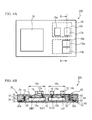
- FIG. 4A illustrates a top view of a circuit substrate 200 in accordance with the second embodiment.
- FIG. 4B illustrates a cross sectional view taken along a line B-B of FIG. 4A .
- whole of the chip components 12a and 16a is inside of the projected region 10c.
- Whole of the chip components 14a and 14b is inside of the projected region 10d. It is therefore possible to downsize the circuit substrate 200 more.
- the interconnection line can be shortened as well as the first embodiment. Therefore, the high frequency characteristic can be improved.
- the chip component 12a is directly connected with the transmit filter chip 10a. Therefore, the chip component 12a may be inside of the projected region 10c.
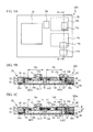
- FIG. 5A illustrates a top view of a circuit substrate 300 in accordance with a third embodiment.
- FIG. 5B illustrates a cross sectional view taken along a line-B-B of FIG. 5A .
- a part of the chip component 14a is inside of the projected region 10d, and another part of the chip component 14a is outside of the projected region 10d.
- the circuit substrate 300 can be downsized, and the high frequency characteristic can be improved. At least a part of one of the chip components 12a, 14a, 14b and 16a has only to be inside of the projected region 10c or the projected region 10d.
- FIG. 5C illustrates a cross sectional view of a circuit substrate 300a in accordance with a modified embodiment of the third embodiment.
- the receive filter chip 10b is connected with the chip component 14a via an interconnection line 40a (first interconnection line, with reference to meshed lines of FIG. 5C ) included in the conductive layer 40 and a via interconnection line 52a (second interconnection line).
- the length L3 of the interconnection line 40a is, for example, 30 ⁇ m.
- the length L1 of the via interconnection line 52a is, for example, 60 ⁇ m.
- the high frequency characteristic can be improved, because the interconnection line 40a extending in the face direction is shorter than the via interconnection line 52a.
- the length of the interconnection line 40a can be changed according to the layout on the upper face of the laminate substrate 28. However, it is preferable that the interconnection line 40a is shorter than the via interconnection line 52a.
- a fourth embodiment is an embodiment in which a core is used.
- FIG. 6 illustrates a cross sectional view of a circuit substrate 400 in accordance with the fourth embodiment.
- the laminate substrate 28 includes a core 54 and an insulating layer 37, the insulating layer 37 being provided between the insulating layer 36 and the insulating layer 38.
- the core 54 has a thickness of 250 ⁇ m or the like and is made of a metal such as copper.
- the core 54 has a ground potential and is connected with the chip component 14b and a ground terminal 50d included in the conductive layer 50.
- the transmit filter chip 10a and the receive filter chip 10b are provided inside of an opening 54a of the core 54.
- the via interconnection line 52 connecting the conductive layer 42 and the conductive layer 48 extends to an opening 54b.
- the core 54 suppresses signal interference between the conductive layers 40 and 42 on the upper side of the core 54 and the conductive layers 48 and 50 on the lower side of the core 54. This results in improvement of the high frequency characteristic.
- the core 54 is made of a metal and is thicker than other conductive layers. Therefore, the intensity and radiation performance of the circuit substrate 400 can be improved.
- the IDT and the terminal of the filter chip may be provided on the upper face of the filter chip, or may be provided on the lower face of the filter chip.
- the filter chip may be another acoustic wave filter chip other than the SAW filter chip such as a boundary acoustic wave filter chip or a FBAR filter chip.
- a duplexer chip in which a transmit filter and a receive filter chip are provided on a single chip may be provided inside of the laminate substrate 28. In this case, a chip component is provided so that the duplexer chip overlaps with a projected region of the laminate substrate 28 projected in the thickness direction of the laminate substrate 28.
- the first embodiment through the fourth embodiment may be applied to an example in which a filter other than the duplexer is provided inside of the laminate substrate 28.
Landscapes
- Physics & Mathematics (AREA)
- Acoustics & Sound (AREA)
- Engineering & Computer Science (AREA)
- Microelectronics & Electronic Packaging (AREA)
- Manufacturing & Machinery (AREA)
- Surface Acoustic Wave Elements And Circuit Networks Thereof (AREA)
- Transceivers (AREA)
- Piezo-Electric Or Mechanical Vibrators, Or Delay Or Filter Circuits (AREA)
Abstract
Description
- A certain aspect of the present invention relates to a circuit substrate.
- There is known an acoustic wave filter such as a SAW (Surface Acoustic Wave) filter or a FBAR (Film Bulk Acoustic Resonator) filter, as a filter being superior in high frequency characteristic. Downsizing of a component including an acoustic wave filter is needed as a mobile communication terminal such as a mobile phone is spread. In order to downsize a component, a circuit substrate in which an acoustic wave filter and an electronic component such as an IC (Integrated Circuit) are provided on an identical substrate is used. Japanese Patent Application Publication No.
2001-189605 2011-176061 - According to an embodiment of the present invention, there is provided a circuit substrate including: a laminate substrate in which a conductive layer and an insulating layer are laminated; a filter chip that has an acoustic wave filter and is provided inside of the laminate substrate; and a chip component that is provided on a surface of the laminate substrate and is connected to the filter chip, at least a part of the chip component overlapping with a projected region that is a region of the filter chip projected in a thickness direction of the laminate substrate.
-
-
FIG. 1A illustrates a schematic view of a module including an acoustic wave filter; -
FIG. 1B illustrates a circuit diagram of a ladder type filter; -
FIG. 2A illustrates a top view of a circuit substrate in accordance with a comparative example; -
FIG. 2B illustrates a cross sectional view taken along a line B-B ofFIG. 2A ; -
FIG. 3A illustrates a top view of a circuit substrate in accordance with a first embodiment; -
FIG. 3B illustrates a cross sectional view taken along a line B-B ofFIG. 3A ; -
FIG. 3C illustrates a perspective view of a chip component; -
FIG. 4A illustrates a top view of a circuit substrate in accordance with a second embodiment; -
FIG. 4B illustrates a cross sectional view taken along a line B-B ofFIG. 4A ; -
FIG. 5A illustrates a top view of a circuit substrate in accordance with a third embodiment; -
FIG. 5B illustrates a cross sectional view taken along a line-B-B ofFIG. 5A ; -
FIG. 5C illustrates a cross sectional view of a circuit substrate in accordance with a modified embodiment of the third embodiment; and -
FIG. 6 illustrates a cross sectional view of a circuit substrate in accordance with a fourth embodiment. - With conventional technology, an interconnection line connecting an acoustic wave filter and an electronic component is long. This results in difficulty of impedance matching and increasing of noise influence. As a result, there was a case where high frequency characteristic of an acoustic wave filter was degraded. And it is difficult to sufficiently downsize a circuit substrate.
- First, a description will be given of a module including an acoustic wave filter.
FIG. 1A illustrates a schematic view of the module including an acoustic wave filter. - As illustrated in
FIG. 1A , aduplexer 10 includes a transmit filter 10Tx and a receive filter 10Rx that are SAW filters or the like. The transmit filter 10Tx is connected between an antenna node Ant1 (common node) and a transmit node Tx1. The receive filter 10Rx is connected between the antenna node Ant1 and a receive node Rx1. The transmit filter 10Tx and the receive filter 10Rx are connected with a ground terminal (not illustrated). An antenna node Ant2 is connected between amatching circuit 12 and aswitch 20. A receive node Rx2 is connected between amatching circuit 14 and an RFIC (Radio Frequency Integrated Circuit) 24 (electronic component). A transmit node Tx2 is connected between aPA 18 and theRFIC 24. - A BBIC (Base Band Integrated Circuit) 26 inputs a transmit signal of a base band into the
RFIC 24. TheRFIC 24 up-converts the transmit signal of the base band into a transmit signal of high frequency. The transmit signal is amplified by the PA (Power Amplifier) 18, passes through amatching circuit 16, and is input into the transmit filter 10Tx. The transmit filter 10Tx allows passage of a signal having a frequency in a pass band of the transmit filter 10Tx included in the transmit signal, and suppresses a signal having a frequency out of the pass band of the transmit filter 10Tx included in the transmit signal. Theswitch 20 is connected with other systems having theduplexer 10, thematching circuits PA 18, theRFIC 24 and the BBIC 26 (not illustrated inFIG. 1A ). For example, theswitch 20 selects one of the systems according to a pass band and connects the one with anantenna 22. The transmit signal is input into theantenna 22 via thematching circuit 12 and theswitch 20 and is transmitted from theantenna 22. A receive signal received by theantenna 22 is input into the receive filter 10Rx via theswitch 20 and thematching circuit 12. The receive filter 10Rx allows passage of a signal having a frequency in a pass band of the receive filter 10Rx included in the receive signal and suppresses a signal having a frequency out of the pass band of the receive filter 10Rx included in the receive signal. The receive signal is input into theRFIC 24 via thematching circuit 14, and is amplified by a low noise amplifier included in theRFIC 24. TheRFIC 24 down-converts the receive signal into a receive signal of the base band. TheBBIC 26 processes the receive signal of the base band. - The matching
circuits duplexer 10, thePA 18, theswitch 20, theantenna 22, theRFIC 24 and theBBIC 26. In order to achieve adequate impedance matching, it is preferable that the matchingcircuits duplexer 10, and interconnection lines connecting between the matchingcircuits duplexer 10 are short. - A ladder type filter or the like is used as the transmit filter 10Tx and the receive filter 10Rx.
FIG. 1B illustrates a circuit diagram of a ladder type filter. Series resonators S1 through S3 are connected in series between an input terminal "In" and an output terminal "Out". A parallel resonator P1 is connected between the series resonators S1 and S2. A parallel resonator P2 is connected between the series resonators S2 and S3. The parallel resonators P1 and P2 are connected with a ground terminal. The input terminal "In" of the transmit filter 10Tx is connected with the transmit node Tx1 ofFIG. 1A . The output terminal "Out" of the transmit filter 10Tx is connected with the antenna node Ant1. The input terminal "In" of the receive filter 10Rx is connected with the antenna node Ant1. The output terminal "Out" of the receive filter 10Rx is connected with the receive node Rx1. A multiple mode filter or the like other than the ladder type filter may be used as the transmit filter 10Tx and the receive filter 10Rx. - A description will be given of an example as a comparative example in which a structure surrounded by a square A in the module is provided on a single circuit substrate.
FIG. 2A illustrates a top view of acircuit substrate 100R in accordance with the comparative example.FIG. 2B illustrates a cross sectional view taken along a line B-B ofFIG. 2A . InFIG. 2A , a solder resist 129 and aconductive layer 140 are not illustrated. InFIG. 2B , a numeral is added to only a part of a plurality of via interconnection lines 152. - As illustrated in
FIG. 2A and FIG. 2B , insulatinglayers conductive layer 140 andconductive layers interconnection line 152 penetrating the insulatinglayers conductive layer 150 acts as a foot pad for connecting alaminate substrate 128 and an external component such as theantenna 22, theRFIC 24 or theBBIC 26. Anantenna terminal 150b of theconductive layer 150 ofFIG. 2B corresponds to the antenna node Ant2 ofFIG. 1A . A receive terminal 150c acts as the receive node Rx2 ofFIG. 1A . A transmit terminal corresponding to the transmit node Tx2 ofFIG. 1A is not illustrated. - A transmit
filter chip 110a is a SAW filter chip or the like including the transmit filter 10Tx ofFIG. 1A . A receivefilter chip 110b is a SAW filter chip or the like including the receive filter 10Rx. The matchingcircuit 12 ofFIG. 1A includes achip component 112a. The matchingcircuit 14 includeschip components circuit 16 includes achip component 116a. Anactive component 118a includes thePA 18. - The transmit
filter chip 110a and the receivefilter chip 110b are flip-chip mounted on theconductive layer 140 provided on an upper face of thelaminate substrate 128. Thechip components conductive layer 140 through asolder 115. A ground terminal GND1 of the transmitfilter chip 110a and a ground terminal GND2 of the receivefilter chip 110b are connected with aground terminal 150a in common. An output terminal Out1 of the transmitfilter chip 110a and an input terminal In2 of the receivefilter chip 110b are connected with thechip component 112a via an interconnection line included in theconductive layer 140. Thechip component 112a is connected with the antenna 22 (FIG. 1A ) via theantenna terminal 150b included in theconductive layer 150. An input terminal In1 of the transmitfilter chip 110a is connected with thechip component 116a (FIG. 2A ) via an interconnection line included in theconductive layer 140. Thechip component 116a is connected with theactive component 118a (FIG. 2A ). Theactive component 118a is connected with the RFIC 24 (FIG. 1 ). The output terminal Out2 of the receivefilter chip 110b is connected with thechip components conductive layer 140. Thechip components FIG. 1A ) via the receive terminal 150c. - The filter chips (the transmit
filter chip 110a and the receivefilter chip 110b), thechip components active component 118a are provided on the upper face of thelaminate substrate 128. Therefore, thelaminate substrate 128 gets larger. The interconnection line extending along a face direction of thelaminate substrate 128 gets longer as well as the interconnection line included in theconductive layer 140, and has a length of 150 µm or more, for example. Therefore, it is difficult to achieve the impedance matching between the filter chips and thechip components circuit substrate 100R may be degraded. Locations of the filter chips, thechip components active component 118a and pathways of the interconnection lines may be limited. Therefore, the interconnection lines get longer, and the high frequency characteristic may be greatly degraded. When both of the filter chips and the chip components are provided inside of thelaminate substrate 128, the interconnection lines get longer because of connections of interconnection lines in the face direction. And it is difficult to change the locations of the filter chips and the chip components that have been provided inside of thelaminate substrate 128 and a circuit constant (resistance value, capacitance and inductance). Therefore, it is difficult to achieve adequate impedance matching while the locations are adjusted. Next, a description will be given of a first embodiment. - A first embodiment is an embodiment in which a filter chip is provided inside of a laminate substrate, and a chip component is mounted on an upper face (surface) of the laminate substrate.
FIG. 3A illustrates a top view of acircuit substrate 100 in accordance with the first embodiment.FIG. 3B illustrates a cross sectional view taken along a line B-B ofFIG. 3A . - As illustrated in
FIG. 3A and FIG. 3B , a transmitfilter chip 10a and a receivefilter chip 10b are SAW filter chips in which an IDT (Interdigital Transducer) is formed on a piezoelectric substrate made of a piezoelectric material such as lithium tantalate (LiTaO3 or lithium niobate (LiNbO3), and are provided inside of alaminate substrate 28. An IDT exciting an acoustic wave is not illustrated, but is provided on the upper face of each filter chip. -
Chip components laminate substrate 28 through asolder 15. Whole of thechip component 12a (first chip component) overlaps with a projectedregion 10c (first projected region, with reference to a broken line) that is a region of the transmitfilter chip 10a projected in a thickness direction of the laminate substrate 28 (up and down direction ofFIG. 3B ). Whole of thechip component 14a (third chip component) overlaps with a projectedregion 10d (second projected region, with reference to a broken line) that is a region of the receivefilter chip 10b projected in the thickness direction of thelaminate substrate 28. Therefore, an area of thelaminate substrate 28 is smaller than the comparative example. It is therefore possible to downsize thecircuit substrate 100. - As illustrated in
FIG. 3B , an output terminal Out1 of the transmitfilter chip 10a and an input terminal In2 of the receivefilter chip 10b are connected with thechip component 12a via a viainterconnection line 52 andconductive layers chip component 12a is connected with an antenna terminal (not illustrated) included in aconductive layer 50. The antenna terminal corresponds to the antenna node Ant2 ofFIG. 1A and is connected with theswitch 20 and theantenna 22. An input terminal (not illustrated) of the transmitfilter chip 10a is connected with thechip component 16a (second chip component, with reference toFIG. 3A ). Thechip component 16a is connected with a transmit terminal (not illustrated) included in theconductive layer 50 via anactive component 18a (FIG. 3A ). The transmit terminal of theconductive layer 50 corresponds to the transmit node Tx2 ofFIG. 1A and is connected with theRFIC 24. The ground terminal GND1 of the transmitfilter chip 10a is connected with aground terminal 50a included in theconductive layer 50 via theconductive layers 42 andconductive layers - The output terminal Out2 of the receive
filter chip 10b is connected with thechip component 14a via the viainterconnection line 52 and theconductive layer 40. Thechip component 14a is connected with a receive terminal 50c included in theconductive layer 50 via thechip component 14b and the viainterconnection line 52. The receive terminal 50c corresponds to the receive node Rx2 ofFIG. 1A and is connected with theRFIC 24. - The
chip component 12a connected with the transmitfilter chip 10a overlaps with the projectedregion 10c. Therefore, the interconnection line connecting the transmitfilter chip 10a and thechip component 12a does not include an interconnection line extending in the face direction, and is structured with the viainterconnection line 52. The interconnection line connecting the receivefilter chip 10b and thechip component 14a is also structured with the viainterconnection line 52. A thickness of insulatinglayers interconnection line 52 connecting the receivefilter chip 10b and thechip component 14a is, for example, 60 µm or the like. The interconnection line connecting the filter chip and thechip components circuit substrate 100 is improved. In order to improve the high frequency characteristic effectively, it is preferable that the transmitfilter chip 10a is directly connected with thechip component 12a not through another chip component, and the receivefilter chip 10b is directly connected with thechip component 14a not through another chip component. - The
chip components laminate substrate 28. It is therefore possible to achieve the impedance matching accurately and easily, while the locations of thechip components laminate substrate 28. Therefore, the freedom degree of the locations of theactive component 18a, thechip components circuit substrate 100 can be downsized, and the interconnection line extending along the face direction can be shortened. -
FIG. 3C illustrates a perspective view of thechip component 12a. A width of thechip component 12a is, for example, 0.4 mm, 0.6 mm, or 1 mm. A length L2 of thechip component 12a is, for example, 0.2 mm, 0.3 mm, or 0.5 mm. A height of thechip component 12a is, for example, 0.3 mm. Thechip components laminate substrate 28. A thickness of the filter chip is, for example, 250 µm. However, the thickness may be changed. The number of the insulating layers and the number of the conductive layers included in thelaminate substrate 28 may be changed. Thecircuit substrate 100 may have at least one of or all of theswitch 20, theantenna 22, theBBIC 26 and theRFIC 24 other than circuit elements surrounded by the square A ofFIG. 1A . - The insulating layers 30 and 32 and insulating
layers conductive layers solder 15 includes tin-silver (Sn-Ag) or the like. A solder resist 29 ofFIG. 3B restrains adhesion of thesolder 15 to undesirable position of thelaminate substrate 28 and theconductive layer 40. - A second embodiment is an embodiment in which a plurality of chip components are provided in a single projected region.
FIG. 4A illustrates a top view of acircuit substrate 200 in accordance with the second embodiment.FIG. 4B illustrates a cross sectional view taken along a line B-B ofFIG. 4A . - As illustrated in
FIG. 4A and FIG. 4B , whole of thechip components region 10c. Whole of thechip components region 10d. It is therefore possible to downsize thecircuit substrate 200 more. The interconnection line can be shortened as well as the first embodiment. Therefore, the high frequency characteristic can be improved. Thechip component 12a is directly connected with the transmitfilter chip 10a. Therefore, thechip component 12a may be inside of the projectedregion 10c. - A third embodiment is an embodiment in which a part of a chip component is provided inside of a projected region.
FIG. 5A illustrates a top view of acircuit substrate 300 in accordance with a third embodiment.FIG. 5B illustrates a cross sectional view taken along a line-B-B ofFIG. 5A . - As illustrated in
FIG. 5A and FIG. 5B , a part of thechip component 14a is inside of the projectedregion 10d, and another part of thechip component 14a is outside of the projectedregion 10d. In accordance with the third embodiment, thecircuit substrate 300 can be downsized, and the high frequency characteristic can be improved. At least a part of one of thechip components region 10c or the projectedregion 10d. -
FIG. 5C illustrates a cross sectional view of acircuit substrate 300a in accordance with a modified embodiment of the third embodiment. As illustrated inFIG. 5C , the receivefilter chip 10b is connected with thechip component 14a via aninterconnection line 40a (first interconnection line, with reference to meshed lines ofFIG. 5C ) included in theconductive layer 40 and a via interconnection line 52a (second interconnection line). The length L3 of theinterconnection line 40a is, for example, 30 µm. The length L1 of the via interconnection line 52a is, for example, 60 µm. Even if the via interconnection line 52a is not provided so as to overlap with thechip component 14a, the high frequency characteristic can be improved, because theinterconnection line 40a extending in the face direction is shorter than the via interconnection line 52a. The length of theinterconnection line 40a can be changed according to the layout on the upper face of thelaminate substrate 28. However, it is preferable that theinterconnection line 40a is shorter than the via interconnection line 52a. - A fourth embodiment is an embodiment in which a core is used.
FIG. 6 illustrates a cross sectional view of acircuit substrate 400 in accordance with the fourth embodiment. - As illustrated in
FIG. 6 , thelaminate substrate 28 includes acore 54 and an insulatinglayer 37, the insulatinglayer 37 being provided between the insulatinglayer 36 and the insulatinglayer 38. Thecore 54 has a thickness of 250 µm or the like and is made of a metal such as copper. Thecore 54 has a ground potential and is connected with thechip component 14b and aground terminal 50d included in theconductive layer 50. The transmitfilter chip 10a and the receivefilter chip 10b are provided inside of anopening 54a of thecore 54. The viainterconnection line 52 connecting theconductive layer 42 and theconductive layer 48 extends to anopening 54b. Thecore 54 suppresses signal interference between theconductive layers core 54 and theconductive layers core 54. This results in improvement of the high frequency characteristic. Thecore 54 is made of a metal and is thicker than other conductive layers. Therefore, the intensity and radiation performance of thecircuit substrate 400 can be improved. - In the first embodiment through the fourth embodiment, the IDT and the terminal of the filter chip may be provided on the upper face of the filter chip, or may be provided on the lower face of the filter chip. The filter chip may be another acoustic wave filter chip other than the SAW filter chip such as a boundary acoustic wave filter chip or a FBAR filter chip. A duplexer chip in which a transmit filter and a receive filter chip are provided on a single chip may be provided inside of the
laminate substrate 28. In this case, a chip component is provided so that the duplexer chip overlaps with a projected region of thelaminate substrate 28 projected in the thickness direction of thelaminate substrate 28. The first embodiment through the fourth embodiment may be applied to an example in which a filter other than the duplexer is provided inside of thelaminate substrate 28. - The present invention is not limited to the specifically described embodiments, but other embodiments and variations may be made without departing from the scope of the claimed invention.
Claims (8)
- A circuit substrate comprising:a laminate substrate in which a conductive layer and an insulating layer are laminated;a filter chip that has an acoustic wave filter and is provided inside of the laminate substrate; anda chip component that is provided on a surface of the laminate substrate and is connected to the filter chip, at least a part of the chip component overlapping with a projected region that is a region of the filter chip projected in a thickness direction of the laminate substrate.
- The circuit substrate as claimed in claim 1, wherein the whole of the chip component is inside of the projected region.
- The circuit substrate as claimed in claim 1 or 2, wherein the whole of a plurality of the chip components is inside of the projected region.
- The circuit substrate as claimed in any of claims 1 to 3, wherein the filter chip is directly connected to the chip component not through another chip component.
- The circuit substrate as claimed in any of claims 1 to 4, wherein a plurality of the filter chips include a transmit filter chip having a transmit filter and a receive filter chip having a receive filter.
- The circuit substrate as claimed in claim 5, wherein:the transmit filter chip is connected between a transmit node and a common node;the receive filter chip is connected between a receive node and the common node;a plurality of the chip components include a first chip component connected between the common node and an antenna, a second chip component connected between the transmit node and an electronic component, and a third chip component connected between the receive node and the electronic component;the first chip component overlaps with one of a first projected region that is a region of the transmit filter chip projected in the thickness direction of the laminate substrate and a second projected region that is a region of the receive filter chip projected in the thickness direction of the laminate substrate;the second chip component overlaps with the first projected region; andthe third chip component overlaps with the second projected region.
- The circuit substrate as claimed in any of claims 1 to 6, wherein:interconnection lines connecting the filter chip and the chip component includes a first interconnection line extending in a face direction of the laminate substrate and a second interconnection line extending in the thickness direction of the laminate substrate; andthe first interconnection line is shorter than the second interconnection line.
- The circuit substrate as claimed in any of claims 1 to 7, wherein:the laminate substrate includes a core made of a metal; andthe filter chip is provided inside of an opening formed in the core.
Applications Claiming Priority (1)
| Application Number | Priority Date | Filing Date | Title |
|---|---|---|---|
| JP2011282012A JP5241909B2 (en) | 2011-12-22 | 2011-12-22 | Circuit board |
Publications (3)
| Publication Number | Publication Date |
|---|---|
| EP2608407A2 true EP2608407A2 (en) | 2013-06-26 |
| EP2608407A3 EP2608407A3 (en) | 2014-05-14 |
| EP2608407B1 EP2608407B1 (en) | 2018-09-19 |
Family
ID=47143615
Family Applications (1)
| Application Number | Title | Priority Date | Filing Date |
|---|---|---|---|
| EP12190574.9A Active EP2608407B1 (en) | 2011-12-22 | 2012-10-30 | Circuit substrate for duplexers |
Country Status (6)
| Country | Link |
|---|---|
| US (2) | US20130162367A1 (en) |
| EP (1) | EP2608407B1 (en) |
| JP (1) | JP5241909B2 (en) |
| KR (1) | KR101389149B1 (en) |
| CN (1) | CN103179779B (en) |
| TW (1) | TWI451818B (en) |
Families Citing this family (11)
| Publication number | Priority date | Publication date | Assignee | Title |
|---|---|---|---|---|
| US9634641B2 (en) | 2013-11-06 | 2017-04-25 | Taiyo Yuden Co., Ltd. | Electronic module having an interconnection substrate with a buried electronic device therein |
| US9263425B2 (en) * | 2013-12-11 | 2016-02-16 | Infineon Technologies Austria Ag | Semiconductor device including multiple semiconductor chips and a laminate |
| JP6368091B2 (en) * | 2014-01-07 | 2018-08-01 | 太陽誘電株式会社 | module |
| WO2016088681A1 (en) * | 2014-12-04 | 2016-06-09 | 株式会社村田製作所 | Electronic component and method for manufacturing same |
| US9660609B2 (en) * | 2015-07-07 | 2017-05-23 | Skyworks Solutions, Inc. | Devices and methods related to stacked duplexers |
| US10312193B2 (en) | 2016-08-12 | 2019-06-04 | Qualcomm Incorporated | Package comprising switches and filters |
| CN111164832B (en) | 2017-09-14 | 2023-11-21 | 株式会社村田制作所 | Antenna modules and communication devices |
| DE102018106028A1 (en) * | 2018-03-15 | 2019-09-19 | RF360 Europe GmbH | Multiplexer and a multiplexer comprehensive front-end module |
| EP3907760A1 (en) * | 2020-05-08 | 2021-11-10 | Infineon Technologies Austria AG | Semiconductor module |
| JP7511028B2 (en) | 2020-05-25 | 2024-07-04 | ケーエムダブリュ・インコーポレーテッド | Antenna Device |
| CN114671395B (en) * | 2020-12-24 | 2026-01-23 | 诺思(天津)微系统有限责任公司 | Semiconductor structure, manufacturing method thereof, MEMS device and electronic equipment |
Citations (2)
| Publication number | Priority date | Publication date | Assignee | Title |
|---|---|---|---|---|
| JP2001189605A (en) | 1999-10-21 | 2001-07-10 | Matsushita Electric Ind Co Ltd | Ceramic multilayer RF device |
| JP2011176061A (en) | 2010-02-23 | 2011-09-08 | Panasonic Corp | Semiconductor device |
Family Cites Families (15)
| Publication number | Priority date | Publication date | Assignee | Title |
|---|---|---|---|---|
| JP3598060B2 (en) * | 1999-12-20 | 2004-12-08 | 松下電器産業株式会社 | CIRCUIT COMPONENT MODULE, MANUFACTURING METHOD THEREOF, AND RADIO DEVICE |
| JP4685979B2 (en) | 2000-02-21 | 2011-05-18 | 日本特殊陶業株式会社 | Wiring board |
| JP3604033B2 (en) * | 2000-09-08 | 2004-12-22 | 日立エーアイシー株式会社 | Multilayer wiring board with built-in electronic components |
| JP3554310B2 (en) * | 2001-03-28 | 2004-08-18 | 京セラ株式会社 | Electronic circuit module |
| JP2002344146A (en) * | 2001-05-15 | 2002-11-29 | Tdk Corp | High frequency module and manufacturing method thereof |
| JP4020644B2 (en) * | 2002-01-09 | 2007-12-12 | アルプス電気株式会社 | SAW filter module |
| US6873529B2 (en) * | 2002-02-26 | 2005-03-29 | Kyocera Corporation | High frequency module |
| JP4000081B2 (en) * | 2003-03-12 | 2007-10-31 | 京セラ株式会社 | Diplexer built-in wiring board |
| TW200520201A (en) * | 2003-10-08 | 2005-06-16 | Kyocera Corp | High-frequency module and communication apparatus |
| DE602005025746D1 (en) * | 2004-04-16 | 2011-02-17 | Nxp Bv | INTEGRATED CIRCUIT, METHOD FOR MANUFACTURING INTEGRATED CIRCUIT AND MOBILE PHONE WITH INTEGRATED CIRCUIT |
| JP2007273585A (en) * | 2006-03-30 | 2007-10-18 | Sony Corp | Micro device module and manufacturing method thereof |
| DE102006016345A1 (en) * | 2006-04-05 | 2007-10-18 | Infineon Technologies Ag | Semiconductor module with discrete components and method for producing the same |
| EP2381576B8 (en) | 2008-12-26 | 2019-01-02 | Taiyo Yuden Co., Ltd. | Demultiplexer and electronic device |
| JP5149881B2 (en) * | 2009-09-30 | 2013-02-20 | ルネサスエレクトロニクス株式会社 | Manufacturing method of semiconductor device |
| JP5241910B2 (en) | 2011-12-22 | 2013-07-17 | 太陽誘電株式会社 | Circuit board |
-
2011
- 2011-12-22 JP JP2011282012A patent/JP5241909B2/en not_active Expired - Fee Related
-
2012
- 2012-10-29 US US13/662,982 patent/US20130162367A1/en not_active Abandoned
- 2012-10-30 EP EP12190574.9A patent/EP2608407B1/en active Active
- 2012-11-01 TW TW101140612A patent/TWI451818B/en active
- 2012-12-12 CN CN201210535433.8A patent/CN103179779B/en active Active
- 2012-12-21 KR KR1020120151060A patent/KR101389149B1/en not_active Expired - Fee Related
-
2014
- 2014-03-26 US US14/226,712 patent/US8917520B2/en active Active
Patent Citations (2)
| Publication number | Priority date | Publication date | Assignee | Title |
|---|---|---|---|---|
| JP2001189605A (en) | 1999-10-21 | 2001-07-10 | Matsushita Electric Ind Co Ltd | Ceramic multilayer RF device |
| JP2011176061A (en) | 2010-02-23 | 2011-09-08 | Panasonic Corp | Semiconductor device |
Also Published As
| Publication number | Publication date |
|---|---|
| CN103179779B (en) | 2016-03-02 |
| EP2608407B1 (en) | 2018-09-19 |
| US20130162367A1 (en) | 2013-06-27 |
| EP2608407A3 (en) | 2014-05-14 |
| TW201328448A (en) | 2013-07-01 |
| US20140204549A1 (en) | 2014-07-24 |
| JP2013132014A (en) | 2013-07-04 |
| TWI451818B (en) | 2014-09-01 |
| JP5241909B2 (en) | 2013-07-17 |
| CN103179779A (en) | 2013-06-26 |
| KR20130079213A (en) | 2013-07-10 |
| KR101389149B1 (en) | 2014-04-24 |
| US8917520B2 (en) | 2014-12-23 |
Similar Documents
| Publication | Publication Date | Title |
|---|---|---|
| EP2608407B1 (en) | Circuit substrate for duplexers | |
| EP2608408B1 (en) | Circuit substrate for duplexers | |
| US10873352B2 (en) | Radio-frequency module and communication apparatus | |
| JP6725059B2 (en) | High frequency module and communication device | |
| KR102930629B1 (en) | High frequency module and communication device | |
| US9287850B2 (en) | Communication module comprised of multiple interdigital transducer duplexers for wireless communication unit | |
| US11451251B2 (en) | Radio frequency module and communication device | |
| KR102455842B1 (en) | Circuit modules and communication devices | |
| WO2018110577A1 (en) | High frequency module and communication device | |
| CN213213453U (en) | High-frequency module and communication device | |
| JP5888786B2 (en) | Circuit board | |
| CN114041265B (en) | High frequency module and communication device | |
| US11239826B2 (en) | Filter device | |
| JP6105358B2 (en) | Circuit board | |
| JP6250935B2 (en) | High frequency module | |
| KR102186689B1 (en) | Multiplexers, high frequency front-end circuits and communication devices |
Legal Events
| Date | Code | Title | Description |
|---|---|---|---|
| AK | Designated contracting states |
Kind code of ref document: A2 Designated state(s): AL AT BE BG CH CY CZ DE DK EE ES FI FR GB GR HR HU IE IS IT LI LT LU LV MC MK MT NL NO PL PT RO RS SE SI SK SM TR |
|
| AX | Request for extension of the european patent |
Extension state: BA ME |
|
| PUAI | Public reference made under article 153(3) epc to a published international application that has entered the european phase |
Free format text: ORIGINAL CODE: 0009012 |
|
| PUAL | Search report despatched |
Free format text: ORIGINAL CODE: 0009013 |
|
| AK | Designated contracting states |
Kind code of ref document: A3 Designated state(s): AL AT BE BG CH CY CZ DE DK EE ES FI FR GB GR HR HU IE IS IT LI LT LU LV MC MK MT NL NO PL PT RO RS SE SI SK SM TR |
|
| AX | Request for extension of the european patent |
Extension state: BA ME |
|
| RIC1 | Information provided on ipc code assigned before grant |
Ipc: H03H 9/72 20060101ALI20140410BHEP Ipc: H03H 9/05 20060101AFI20140410BHEP Ipc: H03H 9/70 20060101ALI20140410BHEP |
|
| 17P | Request for examination filed |
Effective date: 20140820 |
|
| RBV | Designated contracting states (corrected) |
Designated state(s): AL AT BE BG CH CY CZ DE DK EE ES FI FR GB GR HR HU IE IS IT LI LT LU LV MC MK MT NL NO PL PT RO RS SE SI SK SM TR |
|
| 17Q | First examination report despatched |
Effective date: 20151105 |
|
| GRAP | Despatch of communication of intention to grant a patent |
Free format text: ORIGINAL CODE: EPIDOSNIGR1 |
|
| STAA | Information on the status of an ep patent application or granted ep patent |
Free format text: STATUS: GRANT OF PATENT IS INTENDED |
|
| INTG | Intention to grant announced |
Effective date: 20180430 |
|
| GRAS | Grant fee paid |
Free format text: ORIGINAL CODE: EPIDOSNIGR3 |
|
| GRAA | (expected) grant |
Free format text: ORIGINAL CODE: 0009210 |
|
| STAA | Information on the status of an ep patent application or granted ep patent |
Free format text: STATUS: THE PATENT HAS BEEN GRANTED |
|
| RAP1 | Party data changed (applicant data changed or rights of an application transferred) |
Owner name: TAIYO YUDEN CO., LTD. |
|
| AK | Designated contracting states |
Kind code of ref document: B1 Designated state(s): AL AT BE BG CH CY CZ DE DK EE ES FI FR GB GR HR HU IE IS IT LI LT LU LV MC MK MT NL NO PL PT RO RS SE SI SK SM TR |
|
| REG | Reference to a national code |
Ref country code: GB Ref legal event code: FG4D |
|
| REG | Reference to a national code |
Ref country code: CH Ref legal event code: EP |
|
| REG | Reference to a national code |
Ref country code: AT Ref legal event code: REF Ref document number: 1044445 Country of ref document: AT Kind code of ref document: T Effective date: 20181015 |
|
| REG | Reference to a national code |
Ref country code: IE Ref legal event code: FG4D |
|
| REG | Reference to a national code |
Ref country code: DE Ref legal event code: R096 Ref document number: 602012051211 Country of ref document: DE |
|
| REG | Reference to a national code |
Ref country code: NL Ref legal event code: MP Effective date: 20180919 |
|
| PG25 | Lapsed in a contracting state [announced via postgrant information from national office to epo] |
Ref country code: BG Free format text: LAPSE BECAUSE OF FAILURE TO SUBMIT A TRANSLATION OF THE DESCRIPTION OR TO PAY THE FEE WITHIN THE PRESCRIBED TIME-LIMIT Effective date: 20181219 Ref country code: SE Free format text: LAPSE BECAUSE OF FAILURE TO SUBMIT A TRANSLATION OF THE DESCRIPTION OR TO PAY THE FEE WITHIN THE PRESCRIBED TIME-LIMIT Effective date: 20180919 Ref country code: FI Free format text: LAPSE BECAUSE OF FAILURE TO SUBMIT A TRANSLATION OF THE DESCRIPTION OR TO PAY THE FEE WITHIN THE PRESCRIBED TIME-LIMIT Effective date: 20180919 Ref country code: NO Free format text: LAPSE BECAUSE OF FAILURE TO SUBMIT A TRANSLATION OF THE DESCRIPTION OR TO PAY THE FEE WITHIN THE PRESCRIBED TIME-LIMIT Effective date: 20181219 Ref country code: RS Free format text: LAPSE BECAUSE OF FAILURE TO SUBMIT A TRANSLATION OF THE DESCRIPTION OR TO PAY THE FEE WITHIN THE PRESCRIBED TIME-LIMIT Effective date: 20180919 Ref country code: GR Free format text: LAPSE BECAUSE OF FAILURE TO SUBMIT A TRANSLATION OF THE DESCRIPTION OR TO PAY THE FEE WITHIN THE PRESCRIBED TIME-LIMIT Effective date: 20181220 Ref country code: LT Free format text: LAPSE BECAUSE OF FAILURE TO SUBMIT A TRANSLATION OF THE DESCRIPTION OR TO PAY THE FEE WITHIN THE PRESCRIBED TIME-LIMIT Effective date: 20180919 |
|
| REG | Reference to a national code |
Ref country code: LT Ref legal event code: MG4D |
|
| PG25 | Lapsed in a contracting state [announced via postgrant information from national office to epo] |
Ref country code: HR Free format text: LAPSE BECAUSE OF FAILURE TO SUBMIT A TRANSLATION OF THE DESCRIPTION OR TO PAY THE FEE WITHIN THE PRESCRIBED TIME-LIMIT Effective date: 20180919 Ref country code: LV Free format text: LAPSE BECAUSE OF FAILURE TO SUBMIT A TRANSLATION OF THE DESCRIPTION OR TO PAY THE FEE WITHIN THE PRESCRIBED TIME-LIMIT Effective date: 20180919 Ref country code: AL Free format text: LAPSE BECAUSE OF FAILURE TO SUBMIT A TRANSLATION OF THE DESCRIPTION OR TO PAY THE FEE WITHIN THE PRESCRIBED TIME-LIMIT Effective date: 20180919 |
|
| REG | Reference to a national code |
Ref country code: AT Ref legal event code: MK05 Ref document number: 1044445 Country of ref document: AT Kind code of ref document: T Effective date: 20180919 |
|
| PG25 | Lapsed in a contracting state [announced via postgrant information from national office to epo] |
Ref country code: IT Free format text: LAPSE BECAUSE OF FAILURE TO SUBMIT A TRANSLATION OF THE DESCRIPTION OR TO PAY THE FEE WITHIN THE PRESCRIBED TIME-LIMIT Effective date: 20180919 Ref country code: RO Free format text: LAPSE BECAUSE OF FAILURE TO SUBMIT A TRANSLATION OF THE DESCRIPTION OR TO PAY THE FEE WITHIN THE PRESCRIBED TIME-LIMIT Effective date: 20180919 Ref country code: CZ Free format text: LAPSE BECAUSE OF FAILURE TO SUBMIT A TRANSLATION OF THE DESCRIPTION OR TO PAY THE FEE WITHIN THE PRESCRIBED TIME-LIMIT Effective date: 20180919 Ref country code: ES Free format text: LAPSE BECAUSE OF FAILURE TO SUBMIT A TRANSLATION OF THE DESCRIPTION OR TO PAY THE FEE WITHIN THE PRESCRIBED TIME-LIMIT Effective date: 20180919 Ref country code: PL Free format text: LAPSE BECAUSE OF FAILURE TO SUBMIT A TRANSLATION OF THE DESCRIPTION OR TO PAY THE FEE WITHIN THE PRESCRIBED TIME-LIMIT Effective date: 20180919 Ref country code: IS Free format text: LAPSE BECAUSE OF FAILURE TO SUBMIT A TRANSLATION OF THE DESCRIPTION OR TO PAY THE FEE WITHIN THE PRESCRIBED TIME-LIMIT Effective date: 20190119 Ref country code: NL Free format text: LAPSE BECAUSE OF FAILURE TO SUBMIT A TRANSLATION OF THE DESCRIPTION OR TO PAY THE FEE WITHIN THE PRESCRIBED TIME-LIMIT Effective date: 20180919 Ref country code: AT Free format text: LAPSE BECAUSE OF FAILURE TO SUBMIT A TRANSLATION OF THE DESCRIPTION OR TO PAY THE FEE WITHIN THE PRESCRIBED TIME-LIMIT Effective date: 20180919 Ref country code: EE Free format text: LAPSE BECAUSE OF FAILURE TO SUBMIT A TRANSLATION OF THE DESCRIPTION OR TO PAY THE FEE WITHIN THE PRESCRIBED TIME-LIMIT Effective date: 20180919 |
|
| PG25 | Lapsed in a contracting state [announced via postgrant information from national office to epo] |
Ref country code: SM Free format text: LAPSE BECAUSE OF FAILURE TO SUBMIT A TRANSLATION OF THE DESCRIPTION OR TO PAY THE FEE WITHIN THE PRESCRIBED TIME-LIMIT Effective date: 20180919 Ref country code: PT Free format text: LAPSE BECAUSE OF FAILURE TO SUBMIT A TRANSLATION OF THE DESCRIPTION OR TO PAY THE FEE WITHIN THE PRESCRIBED TIME-LIMIT Effective date: 20190119 Ref country code: SK Free format text: LAPSE BECAUSE OF FAILURE TO SUBMIT A TRANSLATION OF THE DESCRIPTION OR TO PAY THE FEE WITHIN THE PRESCRIBED TIME-LIMIT Effective date: 20180919 |
|
| REG | Reference to a national code |
Ref country code: CH Ref legal event code: PL |
|
| REG | Reference to a national code |
Ref country code: DE Ref legal event code: R097 Ref document number: 602012051211 Country of ref document: DE |
|
| REG | Reference to a national code |
Ref country code: BE Ref legal event code: MM Effective date: 20181031 |
|
| PG25 | Lapsed in a contracting state [announced via postgrant information from national office to epo] |
Ref country code: LU Free format text: LAPSE BECAUSE OF NON-PAYMENT OF DUE FEES Effective date: 20181030 |
|
| REG | Reference to a national code |
Ref country code: IE Ref legal event code: MM4A |
|
| PLBE | No opposition filed within time limit |
Free format text: ORIGINAL CODE: 0009261 |
|
| STAA | Information on the status of an ep patent application or granted ep patent |
Free format text: STATUS: NO OPPOSITION FILED WITHIN TIME LIMIT |
|
| PG25 | Lapsed in a contracting state [announced via postgrant information from national office to epo] |
Ref country code: DK Free format text: LAPSE BECAUSE OF FAILURE TO SUBMIT A TRANSLATION OF THE DESCRIPTION OR TO PAY THE FEE WITHIN THE PRESCRIBED TIME-LIMIT Effective date: 20180919 Ref country code: MC Free format text: LAPSE BECAUSE OF FAILURE TO SUBMIT A TRANSLATION OF THE DESCRIPTION OR TO PAY THE FEE WITHIN THE PRESCRIBED TIME-LIMIT Effective date: 20180919 |
|
| 26N | No opposition filed |
Effective date: 20190620 |
|
| GBPC | Gb: european patent ceased through non-payment of renewal fee |
Effective date: 20181219 |
|
| PG25 | Lapsed in a contracting state [announced via postgrant information from national office to epo] |
Ref country code: LI Free format text: LAPSE BECAUSE OF NON-PAYMENT OF DUE FEES Effective date: 20181031 Ref country code: CH Free format text: LAPSE BECAUSE OF NON-PAYMENT OF DUE FEES Effective date: 20181031 Ref country code: BE Free format text: LAPSE BECAUSE OF NON-PAYMENT OF DUE FEES Effective date: 20181031 |
|
| PG25 | Lapsed in a contracting state [announced via postgrant information from national office to epo] |
Ref country code: FR Free format text: LAPSE BECAUSE OF NON-PAYMENT OF DUE FEES Effective date: 20181119 Ref country code: SI Free format text: LAPSE BECAUSE OF FAILURE TO SUBMIT A TRANSLATION OF THE DESCRIPTION OR TO PAY THE FEE WITHIN THE PRESCRIBED TIME-LIMIT Effective date: 20180919 Ref country code: IE Free format text: LAPSE BECAUSE OF NON-PAYMENT OF DUE FEES Effective date: 20181030 |
|
| PG25 | Lapsed in a contracting state [announced via postgrant information from national office to epo] |
Ref country code: GB Free format text: LAPSE BECAUSE OF NON-PAYMENT OF DUE FEES Effective date: 20181219 |
|
| PG25 | Lapsed in a contracting state [announced via postgrant information from national office to epo] |
Ref country code: MT Free format text: LAPSE BECAUSE OF NON-PAYMENT OF DUE FEES Effective date: 20181030 |
|
| PG25 | Lapsed in a contracting state [announced via postgrant information from national office to epo] |
Ref country code: TR Free format text: LAPSE BECAUSE OF FAILURE TO SUBMIT A TRANSLATION OF THE DESCRIPTION OR TO PAY THE FEE WITHIN THE PRESCRIBED TIME-LIMIT Effective date: 20180919 |
|
| PG25 | Lapsed in a contracting state [announced via postgrant information from national office to epo] |
Ref country code: CY Free format text: LAPSE BECAUSE OF FAILURE TO SUBMIT A TRANSLATION OF THE DESCRIPTION OR TO PAY THE FEE WITHIN THE PRESCRIBED TIME-LIMIT Effective date: 20180919 Ref country code: HU Free format text: LAPSE BECAUSE OF FAILURE TO SUBMIT A TRANSLATION OF THE DESCRIPTION OR TO PAY THE FEE WITHIN THE PRESCRIBED TIME-LIMIT; INVALID AB INITIO Effective date: 20121030 Ref country code: MK Free format text: LAPSE BECAUSE OF NON-PAYMENT OF DUE FEES Effective date: 20180919 |
|
| REG | Reference to a national code |
Ref country code: DE Ref legal event code: R082 Ref document number: 602012051211 Country of ref document: DE Representative=s name: HL KEMPNER PATENTANWAELTE, SOLICITORS (ENGLAND, DE Ref country code: DE Ref legal event code: R082 Ref document number: 602012051211 Country of ref document: DE Representative=s name: HL KEMPNER PATENTANWALT, RECHTSANWALT, SOLICIT, DE Ref country code: DE Ref legal event code: R082 Ref document number: 602012051211 Country of ref document: DE Representative=s name: HL KEMPNER PARTG MBB, DE |
|
| P01 | Opt-out of the competence of the unified patent court (upc) registered |
Effective date: 20230509 |
|
| PGFP | Annual fee paid to national office [announced via postgrant information from national office to epo] |
Ref country code: DE Payment date: 20250902 Year of fee payment: 14 |