EP2608260A2 - Heterogeneous Chip Integration with Low Loss Interconnection Through Adaptive Patterning - Google Patents
Heterogeneous Chip Integration with Low Loss Interconnection Through Adaptive Patterning Download PDFInfo
- Publication number
- EP2608260A2 EP2608260A2 EP12179960.5A EP12179960A EP2608260A2 EP 2608260 A2 EP2608260 A2 EP 2608260A2 EP 12179960 A EP12179960 A EP 12179960A EP 2608260 A2 EP2608260 A2 EP 2608260A2
- Authority
- EP
- European Patent Office
- Prior art keywords
- layer
- semiconductor component
- electrical
- cavity
- top surface
- Prior art date
- Legal status (The legal status is an assumption and is not a legal conclusion. Google has not performed a legal analysis and makes no representation as to the accuracy of the status listed.)
- Withdrawn
Links
Images

Classifications
-
- H—ELECTRICITY
- H10—SEMICONDUCTOR DEVICES; ELECTRIC SOLID-STATE DEVICES NOT OTHERWISE PROVIDED FOR
- H10W—GENERIC PACKAGES, INTERCONNECTIONS, CONNECTORS OR OTHER CONSTRUCTIONAL DETAILS OF DEVICES COVERED BY CLASS H10
- H10W70/00—Package substrates; Interposers; Redistribution layers [RDL]
- H10W70/60—Insulating or insulated package substrates; Interposers; Redistribution layers
- H10W70/67—Insulating or insulated package substrates; Interposers; Redistribution layers characterised by their insulating layers or insulating parts
- H10W70/68—Shapes or dispositions thereof
- H10W70/6875—Shapes or dispositions thereof being on a metallic substrate, e.g. insulated metal substrates [IMS]
-
- H—ELECTRICITY
- H05—ELECTRIC TECHNIQUES NOT OTHERWISE PROVIDED FOR
- H05K—PRINTED CIRCUITS; CASINGS OR CONSTRUCTIONAL DETAILS OF ELECTRIC APPARATUS; MANUFACTURE OF ASSEMBLAGES OF ELECTRICAL COMPONENTS
- H05K1/00—Printed circuits
- H05K1/18—Printed circuits structurally associated with non-printed electric components
-
- H—ELECTRICITY
- H05—ELECTRIC TECHNIQUES NOT OTHERWISE PROVIDED FOR
- H05K—PRINTED CIRCUITS; CASINGS OR CONSTRUCTIONAL DETAILS OF ELECTRIC APPARATUS; MANUFACTURE OF ASSEMBLAGES OF ELECTRICAL COMPONENTS
- H05K3/00—Apparatus or processes for manufacturing printed circuits
- H05K3/46—Manufacturing multilayer circuits
-
- H—ELECTRICITY
- H10—SEMICONDUCTOR DEVICES; ELECTRIC SOLID-STATE DEVICES NOT OTHERWISE PROVIDED FOR
- H10W—GENERIC PACKAGES, INTERCONNECTIONS, CONNECTORS OR OTHER CONSTRUCTIONAL DETAILS OF DEVICES COVERED BY CLASS H10
- H10W40/00—Arrangements for thermal protection or thermal control
- H10W40/10—Arrangements for heating
-
- H—ELECTRICITY
- H10—SEMICONDUCTOR DEVICES; ELECTRIC SOLID-STATE DEVICES NOT OTHERWISE PROVIDED FOR
- H10W—GENERIC PACKAGES, INTERCONNECTIONS, CONNECTORS OR OTHER CONSTRUCTIONAL DETAILS OF DEVICES COVERED BY CLASS H10
- H10W40/00—Arrangements for thermal protection or thermal control
- H10W40/20—Arrangements for cooling
- H10W40/25—Arrangements for cooling characterised by their materials
- H10W40/258—Metallic materials
-
- H—ELECTRICITY
- H10—SEMICONDUCTOR DEVICES; ELECTRIC SOLID-STATE DEVICES NOT OTHERWISE PROVIDED FOR
- H10W—GENERIC PACKAGES, INTERCONNECTIONS, CONNECTORS OR OTHER CONSTRUCTIONAL DETAILS OF DEVICES COVERED BY CLASS H10
- H10W46/00—Marks applied to devices, e.g. for alignment or identification
-
- H—ELECTRICITY
- H10—SEMICONDUCTOR DEVICES; ELECTRIC SOLID-STATE DEVICES NOT OTHERWISE PROVIDED FOR
- H10W—GENERIC PACKAGES, INTERCONNECTIONS, CONNECTORS OR OTHER CONSTRUCTIONAL DETAILS OF DEVICES COVERED BY CLASS H10
- H10W70/00—Package substrates; Interposers; Redistribution layers [RDL]
- H10W70/01—Manufacture or treatment
- H10W70/05—Manufacture or treatment of insulating or insulated package substrates, or of interposers, or of redistribution layers
- H10W70/08—Manufacture or treatment of insulating or insulated package substrates, or of interposers, or of redistribution layers by depositing layers on the chip or wafer, e.g. "chip-first" RDLs
- H10W70/09—Manufacture or treatment of insulating or insulated package substrates, or of interposers, or of redistribution layers by depositing layers on the chip or wafer, e.g. "chip-first" RDLs extending onto an encapsulation that laterally surrounds the chip or wafer, e.g. fan-out wafer level package [FOWLP] RDLs
-
- H—ELECTRICITY
- H10—SEMICONDUCTOR DEVICES; ELECTRIC SOLID-STATE DEVICES NOT OTHERWISE PROVIDED FOR
- H10W—GENERIC PACKAGES, INTERCONNECTIONS, CONNECTORS OR OTHER CONSTRUCTIONAL DETAILS OF DEVICES COVERED BY CLASS H10
- H10W70/00—Package substrates; Interposers; Redistribution layers [RDL]
- H10W70/60—Insulating or insulated package substrates; Interposers; Redistribution layers
- H10W70/611—Insulating or insulated package substrates; Interposers; Redistribution layers for connecting multiple chips together
- H10W70/614—Insulating or insulated package substrates; Interposers; Redistribution layers for connecting multiple chips together the multiple chips being integrally enclosed
-
- H—ELECTRICITY
- H10—SEMICONDUCTOR DEVICES; ELECTRIC SOLID-STATE DEVICES NOT OTHERWISE PROVIDED FOR
- H10W—GENERIC PACKAGES, INTERCONNECTIONS, CONNECTORS OR OTHER CONSTRUCTIONAL DETAILS OF DEVICES COVERED BY CLASS H10
- H10W70/00—Package substrates; Interposers; Redistribution layers [RDL]
- H10W70/60—Insulating or insulated package substrates; Interposers; Redistribution layers
- H10W70/67—Insulating or insulated package substrates; Interposers; Redistribution layers characterised by their insulating layers or insulating parts
- H10W70/68—Shapes or dispositions thereof
-
- H—ELECTRICITY
- H10—SEMICONDUCTOR DEVICES; ELECTRIC SOLID-STATE DEVICES NOT OTHERWISE PROVIDED FOR
- H10W—GENERIC PACKAGES, INTERCONNECTIONS, CONNECTORS OR OTHER CONSTRUCTIONAL DETAILS OF DEVICES COVERED BY CLASS H10
- H10W72/00—Interconnections or connectors in packages
- H10W72/20—Bump connectors, e.g. solder bumps or copper pillars; Dummy bumps; Thermal bumps
-
- H—ELECTRICITY
- H05—ELECTRIC TECHNIQUES NOT OTHERWISE PROVIDED FOR
- H05K—PRINTED CIRCUITS; CASINGS OR CONSTRUCTIONAL DETAILS OF ELECTRIC APPARATUS; MANUFACTURE OF ASSEMBLAGES OF ELECTRICAL COMPONENTS
- H05K1/00—Printed circuits
- H05K1/18—Printed circuits structurally associated with non-printed electric components
- H05K1/182—Printed circuits structurally associated with non-printed electric components associated with components mounted in printed circuit boards [PCB], e.g. insert-mounted components [IMC]
- H05K1/185—Printed circuits structurally associated with non-printed electric components associated with components mounted in printed circuit boards [PCB], e.g. insert-mounted components [IMC] associated with components encapsulated in the insulating substrate of the PCBs; associated with components incorporated in internal layers of multilayer circuit boards
-
- H—ELECTRICITY
- H10—SEMICONDUCTOR DEVICES; ELECTRIC SOLID-STATE DEVICES NOT OTHERWISE PROVIDED FOR
- H10W—GENERIC PACKAGES, INTERCONNECTIONS, CONNECTORS OR OTHER CONSTRUCTIONAL DETAILS OF DEVICES COVERED BY CLASS H10
- H10W46/00—Marks applied to devices, e.g. for alignment or identification
- H10W46/101—Marks applied to devices, e.g. for alignment or identification characterised by the type of information, e.g. logos or symbols
-
- H—ELECTRICITY
- H10—SEMICONDUCTOR DEVICES; ELECTRIC SOLID-STATE DEVICES NOT OTHERWISE PROVIDED FOR
- H10W—GENERIC PACKAGES, INTERCONNECTIONS, CONNECTORS OR OTHER CONSTRUCTIONAL DETAILS OF DEVICES COVERED BY CLASS H10
- H10W46/00—Marks applied to devices, e.g. for alignment or identification
- H10W46/301—Marks applied to devices, e.g. for alignment or identification for alignment
-
- H—ELECTRICITY
- H10—SEMICONDUCTOR DEVICES; ELECTRIC SOLID-STATE DEVICES NOT OTHERWISE PROVIDED FOR
- H10W—GENERIC PACKAGES, INTERCONNECTIONS, CONNECTORS OR OTHER CONSTRUCTIONAL DETAILS OF DEVICES COVERED BY CLASS H10
- H10W46/00—Marks applied to devices, e.g. for alignment or identification
- H10W46/601—Marks applied to devices, e.g. for alignment or identification for use after dicing
-
- H—ELECTRICITY
- H10—SEMICONDUCTOR DEVICES; ELECTRIC SOLID-STATE DEVICES NOT OTHERWISE PROVIDED FOR
- H10W—GENERIC PACKAGES, INTERCONNECTIONS, CONNECTORS OR OTHER CONSTRUCTIONAL DETAILS OF DEVICES COVERED BY CLASS H10
- H10W70/00—Package substrates; Interposers; Redistribution layers [RDL]
- H10W70/099—Connecting interconnections to insulating or insulated package substrates, interposers or redistribution layers
-
- H—ELECTRICITY
- H10—SEMICONDUCTOR DEVICES; ELECTRIC SOLID-STATE DEVICES NOT OTHERWISE PROVIDED FOR
- H10W—GENERIC PACKAGES, INTERCONNECTIONS, CONNECTORS OR OTHER CONSTRUCTIONAL DETAILS OF DEVICES COVERED BY CLASS H10
- H10W70/00—Package substrates; Interposers; Redistribution layers [RDL]
- H10W70/60—Insulating or insulated package substrates; Interposers; Redistribution layers
-
- H—ELECTRICITY
- H10—SEMICONDUCTOR DEVICES; ELECTRIC SOLID-STATE DEVICES NOT OTHERWISE PROVIDED FOR
- H10W—GENERIC PACKAGES, INTERCONNECTIONS, CONNECTORS OR OTHER CONSTRUCTIONAL DETAILS OF DEVICES COVERED BY CLASS H10
- H10W70/00—Package substrates; Interposers; Redistribution layers [RDL]
- H10W70/60—Insulating or insulated package substrates; Interposers; Redistribution layers
- H10W70/62—Insulating or insulated package substrates; Interposers; Redistribution layers characterised by their interconnections
- H10W70/65—Shapes or dispositions of interconnections
- H10W70/652—Cross-sectional shapes
- H10W70/6528—Cross-sectional shapes of the portions that connect to chips, wafers or package parts
-
- H—ELECTRICITY
- H10—SEMICONDUCTOR DEVICES; ELECTRIC SOLID-STATE DEVICES NOT OTHERWISE PROVIDED FOR
- H10W—GENERIC PACKAGES, INTERCONNECTIONS, CONNECTORS OR OTHER CONSTRUCTIONAL DETAILS OF DEVICES COVERED BY CLASS H10
- H10W70/00—Package substrates; Interposers; Redistribution layers [RDL]
- H10W70/60—Insulating or insulated package substrates; Interposers; Redistribution layers
- H10W70/62—Insulating or insulated package substrates; Interposers; Redistribution layers characterised by their interconnections
- H10W70/65—Shapes or dispositions of interconnections
- H10W70/654—Top-view layouts
- H10W70/655—Fan-out layouts
-
- H—ELECTRICITY
- H10—SEMICONDUCTOR DEVICES; ELECTRIC SOLID-STATE DEVICES NOT OTHERWISE PROVIDED FOR
- H10W—GENERIC PACKAGES, INTERCONNECTIONS, CONNECTORS OR OTHER CONSTRUCTIONAL DETAILS OF DEVICES COVERED BY CLASS H10
- H10W70/00—Package substrates; Interposers; Redistribution layers [RDL]
- H10W70/60—Insulating or insulated package substrates; Interposers; Redistribution layers
- H10W70/67—Insulating or insulated package substrates; Interposers; Redistribution layers characterised by their insulating layers or insulating parts
- H10W70/68—Shapes or dispositions thereof
- H10W70/682—Shapes or dispositions thereof comprising holes having chips therein
-
- H—ELECTRICITY
- H10—SEMICONDUCTOR DEVICES; ELECTRIC SOLID-STATE DEVICES NOT OTHERWISE PROVIDED FOR
- H10W—GENERIC PACKAGES, INTERCONNECTIONS, CONNECTORS OR OTHER CONSTRUCTIONAL DETAILS OF DEVICES COVERED BY CLASS H10
- H10W72/00—Interconnections or connectors in packages
- H10W72/01—Manufacture or treatment
- H10W72/013—Manufacture or treatment of die-attach connectors
- H10W72/01321—Manufacture or treatment of die-attach connectors using local deposition
- H10W72/01323—Manufacture or treatment of die-attach connectors using local deposition in liquid form, e.g. by dispensing droplets or by screen printing
-
- H—ELECTRICITY
- H10—SEMICONDUCTOR DEVICES; ELECTRIC SOLID-STATE DEVICES NOT OTHERWISE PROVIDED FOR
- H10W—GENERIC PACKAGES, INTERCONNECTIONS, CONNECTORS OR OTHER CONSTRUCTIONAL DETAILS OF DEVICES COVERED BY CLASS H10
- H10W72/00—Interconnections or connectors in packages
- H10W72/01—Manufacture or treatment
- H10W72/013—Manufacture or treatment of die-attach connectors
- H10W72/01321—Manufacture or treatment of die-attach connectors using local deposition
- H10W72/01325—Manufacture or treatment of die-attach connectors using local deposition in solid form
-
- H—ELECTRICITY
- H10—SEMICONDUCTOR DEVICES; ELECTRIC SOLID-STATE DEVICES NOT OTHERWISE PROVIDED FOR
- H10W—GENERIC PACKAGES, INTERCONNECTIONS, CONNECTORS OR OTHER CONSTRUCTIONAL DETAILS OF DEVICES COVERED BY CLASS H10
- H10W72/00—Interconnections or connectors in packages
- H10W72/071—Connecting or disconnecting
- H10W72/073—Connecting or disconnecting of die-attach connectors
-
- H—ELECTRICITY
- H10—SEMICONDUCTOR DEVICES; ELECTRIC SOLID-STATE DEVICES NOT OTHERWISE PROVIDED FOR
- H10W—GENERIC PACKAGES, INTERCONNECTIONS, CONNECTORS OR OTHER CONSTRUCTIONAL DETAILS OF DEVICES COVERED BY CLASS H10
- H10W72/00—Interconnections or connectors in packages
- H10W72/071—Connecting or disconnecting
- H10W72/073—Connecting or disconnecting of die-attach connectors
- H10W72/07321—Aligning
- H10W72/07323—Active alignment, e.g. using optical alignment using marks or sensors
-
- H—ELECTRICITY
- H10—SEMICONDUCTOR DEVICES; ELECTRIC SOLID-STATE DEVICES NOT OTHERWISE PROVIDED FOR
- H10W—GENERIC PACKAGES, INTERCONNECTIONS, CONNECTORS OR OTHER CONSTRUCTIONAL DETAILS OF DEVICES COVERED BY CLASS H10
- H10W72/00—Interconnections or connectors in packages
- H10W72/071—Connecting or disconnecting
- H10W72/073—Connecting or disconnecting of die-attach connectors
- H10W72/07331—Connecting techniques
- H10W72/07336—Soldering or alloying
-
- H—ELECTRICITY
- H10—SEMICONDUCTOR DEVICES; ELECTRIC SOLID-STATE DEVICES NOT OTHERWISE PROVIDED FOR
- H10W—GENERIC PACKAGES, INTERCONNECTIONS, CONNECTORS OR OTHER CONSTRUCTIONAL DETAILS OF DEVICES COVERED BY CLASS H10
- H10W72/00—Interconnections or connectors in packages
- H10W72/071—Connecting or disconnecting
- H10W72/073—Connecting or disconnecting of die-attach connectors
- H10W72/07331—Connecting techniques
- H10W72/07337—Connecting techniques using a polymer adhesive, e.g. an adhesive based on silicone or epoxy
-
- H—ELECTRICITY
- H10—SEMICONDUCTOR DEVICES; ELECTRIC SOLID-STATE DEVICES NOT OTHERWISE PROVIDED FOR
- H10W—GENERIC PACKAGES, INTERCONNECTIONS, CONNECTORS OR OTHER CONSTRUCTIONAL DETAILS OF DEVICES COVERED BY CLASS H10
- H10W72/00—Interconnections or connectors in packages
- H10W72/071—Connecting or disconnecting
- H10W72/073—Connecting or disconnecting of die-attach connectors
- H10W72/07331—Connecting techniques
- H10W72/07337—Connecting techniques using a polymer adhesive, e.g. an adhesive based on silicone or epoxy
- H10W72/07338—Connecting techniques using a polymer adhesive, e.g. an adhesive based on silicone or epoxy hardening the adhesive by curing, e.g. thermosetting
-
- H—ELECTRICITY
- H10—SEMICONDUCTOR DEVICES; ELECTRIC SOLID-STATE DEVICES NOT OTHERWISE PROVIDED FOR
- H10W—GENERIC PACKAGES, INTERCONNECTIONS, CONNECTORS OR OTHER CONSTRUCTIONAL DETAILS OF DEVICES COVERED BY CLASS H10
- H10W72/00—Interconnections or connectors in packages
- H10W72/071—Connecting or disconnecting
- H10W72/074—Connecting or disconnecting of anisotropic conductive adhesives
-
- H—ELECTRICITY
- H10—SEMICONDUCTOR DEVICES; ELECTRIC SOLID-STATE DEVICES NOT OTHERWISE PROVIDED FOR
- H10W—GENERIC PACKAGES, INTERCONNECTIONS, CONNECTORS OR OTHER CONSTRUCTIONAL DETAILS OF DEVICES COVERED BY CLASS H10
- H10W72/00—Interconnections or connectors in packages
- H10W72/30—Die-attach connectors
- H10W72/321—Structures or relative sizes of die-attach connectors
- H10W72/325—Die-attach connectors having a filler embedded in a matrix
-
- H—ELECTRICITY
- H10—SEMICONDUCTOR DEVICES; ELECTRIC SOLID-STATE DEVICES NOT OTHERWISE PROVIDED FOR
- H10W—GENERIC PACKAGES, INTERCONNECTIONS, CONNECTORS OR OTHER CONSTRUCTIONAL DETAILS OF DEVICES COVERED BY CLASS H10
- H10W72/00—Interconnections or connectors in packages
- H10W72/30—Die-attach connectors
- H10W72/351—Materials of die-attach connectors
- H10W72/352—Materials of die-attach connectors comprising metals or metalloids, e.g. solders
-
- H—ELECTRICITY
- H10—SEMICONDUCTOR DEVICES; ELECTRIC SOLID-STATE DEVICES NOT OTHERWISE PROVIDED FOR
- H10W—GENERIC PACKAGES, INTERCONNECTIONS, CONNECTORS OR OTHER CONSTRUCTIONAL DETAILS OF DEVICES COVERED BY CLASS H10
- H10W72/00—Interconnections or connectors in packages
- H10W72/30—Die-attach connectors
- H10W72/351—Materials of die-attach connectors
- H10W72/353—Materials of die-attach connectors not comprising solid metals or solid metalloids, e.g. ceramics
-
- H—ELECTRICITY
- H10—SEMICONDUCTOR DEVICES; ELECTRIC SOLID-STATE DEVICES NOT OTHERWISE PROVIDED FOR
- H10W—GENERIC PACKAGES, INTERCONNECTIONS, CONNECTORS OR OTHER CONSTRUCTIONAL DETAILS OF DEVICES COVERED BY CLASS H10
- H10W72/00—Interconnections or connectors in packages
- H10W72/851—Dispositions of multiple connectors or interconnections
- H10W72/874—On different surfaces
-
- H—ELECTRICITY
- H10—SEMICONDUCTOR DEVICES; ELECTRIC SOLID-STATE DEVICES NOT OTHERWISE PROVIDED FOR
- H10W—GENERIC PACKAGES, INTERCONNECTIONS, CONNECTORS OR OTHER CONSTRUCTIONAL DETAILS OF DEVICES COVERED BY CLASS H10
- H10W72/00—Interconnections or connectors in packages
- H10W72/90—Bond pads, in general
- H10W72/921—Structures or relative sizes of bond pads
- H10W72/922—Bond pads being integral with underlying chip-level interconnections
-
- H—ELECTRICITY
- H10—SEMICONDUCTOR DEVICES; ELECTRIC SOLID-STATE DEVICES NOT OTHERWISE PROVIDED FOR
- H10W—GENERIC PACKAGES, INTERCONNECTIONS, CONNECTORS OR OTHER CONSTRUCTIONAL DETAILS OF DEVICES COVERED BY CLASS H10
- H10W72/00—Interconnections or connectors in packages
- H10W72/90—Bond pads, in general
- H10W72/941—Dispositions of bond pads
- H10W72/9413—Dispositions of bond pads on encapsulations
-
- H—ELECTRICITY
- H10—SEMICONDUCTOR DEVICES; ELECTRIC SOLID-STATE DEVICES NOT OTHERWISE PROVIDED FOR
- H10W—GENERIC PACKAGES, INTERCONNECTIONS, CONNECTORS OR OTHER CONSTRUCTIONAL DETAILS OF DEVICES COVERED BY CLASS H10
- H10W76/00—Containers; Fillings or auxiliary members therefor; Seals
- H10W76/10—Containers or parts thereof
- H10W76/12—Containers or parts thereof characterised by their shape
- H10W76/13—Containers comprising a conductive base serving as an interconnection
-
- H—ELECTRICITY
- H10—SEMICONDUCTOR DEVICES; ELECTRIC SOLID-STATE DEVICES NOT OTHERWISE PROVIDED FOR
- H10W—GENERIC PACKAGES, INTERCONNECTIONS, CONNECTORS OR OTHER CONSTRUCTIONAL DETAILS OF DEVICES COVERED BY CLASS H10
- H10W90/00—Package configurations
- H10W90/701—Package configurations characterised by the relative positions of pads or connectors relative to package parts
- H10W90/731—Package configurations characterised by the relative positions of pads or connectors relative to package parts of die-attach connectors
- H10W90/736—Package configurations characterised by the relative positions of pads or connectors relative to package parts of die-attach connectors between a chip and a stacked lead frame, conducting package substrate or heat sink
Definitions
- the currently described invention relates to systems and methods for integrating semiconductor components, including active and passive devices, with a substrate.
- Semiconductor integration methods typically involve connecting active and/or passive elements with passive circuitry via wire or ribbon bonds or flip chip bumps that manifest parasitic behavior at higher frequencies (i.e., at or greater than 10 GHz).
- discontinuities in RF (radio frequency) transmission lines are caused by discontinuities in dielectric properties of underlying material and air gaps between bridged materials (e.g., discontinuity between the dielectric of a substrate material to air).
- the ribbon bond, flip chip technique compromises performance in high radio frequency applications.
- placement inaccuracies between a semiconductor component and a substrate are typically overcome by increasing landing pad dimensions, which results in a substantial increase in radio frequency signal loss at the transition between the semiconductor component and the substrate. These placement inaccuracies also result in requiring a greater pitch between components on the substrate, and increased size and associated cost of the substrate and components.
- One embodiment is a method for integrating a semiconductor component with a layered substrate.
- the method includes forming a cavity in a layered substrate.
- the layered substrate includes a first layer disposed over a second layer of the layered substrate such that the second layer defines the cavity bottom.
- the method also includes disposing a semiconductor component in the cavity such that a top surface of an electrical contact on the semiconductor component is substantially coplanar with the top surface of an electrical trace on the first layer of the layered substrate.
- the method also includes locating at least one fixed fiducial on the first layer.
- the method also includes locating at least one fixed fiducial on the semiconductor component.
- the method also includes forming an electrical interconnect between the electrical trace on the first layer and the electrical contact on the semiconductor component based on the relative positions of the at least one fixed fiducial on the first layer and the at least one fixed fiducial on the semiconductor component, wherein the position of the electrical trace on the first layer is fixed relative to the at least one fixed fiducial on the first layer and the position of the electrical contact on the semiconductor component is fixed relative to the at least one fixed fiducial on the semiconductor component.
- the step of forming the cavity includes sizing the cavity such that a gap of 0-40 microns exists between the semiconductor component and walls of the cavity. In some embodiments, a gap of 25-35 microns exists between the semiconductor component and the walls of the cavity. In some embodiments, the method includes filling the gap between the semiconductor and the walls of the cavity with dielectric material such that a top surface of the dielectric material is substantially coplanar with the top surface of the semiconductor component and the top surface of the first layer. In some embodiments, the method optionally includes applying an adhesive between the cavity bottom and the semiconductor component. In some embodiments, the method optionally includes applying a solder between the cavity bottom and the semiconductor component.
- the method includes disposing the semiconductor component in the cavity such that the electrical contact on the top surface of the semiconductor component is substantially aligned with the electrical trace on the first layer of the layered substrate, wherein alignment includes locating the relative positions of the at least one fixed fiducial on the first layer and the at least one fixed fiducial on the semiconductor component.
- the method includes patterning the electrical trace to compensate for variation in interconnect length between one or more contacts on the semiconductor component and one or more corresponding electrical traces. In one embodiment, the method includes at least one of stretching, compressing, translating or rotating the electrical trace pattern to accommodate for variation in placement of the semiconductor component within the cavity.
- the method includes using a low energy laser to locally develop a photoresist applied to the electrical device, thereby adaptively patterning each individual electrical interconnect extending between one of the one or more contacts and a corresponding one of the one or more electrical traces, thereby accommodating misalignment.
- the low energy laser is a 355 nm laser producing 3.5 mw of power at a laser firing frequency of 30 KHz with a linear scan rate of 52 mm/sec and having a laser spot size of 16 microns.
- the method includes forming the electrical interconnect using one of a pen, a stamping process, or a direct write process that direct writes conductors made of gold, silver, or copper.
- the method includes coating a first layer of photoresist across the top surfaces of the first layer and semiconductor component, opening the first layer of photoresist with laser exposure and development along the electrical interconnect pattern.
- the method includes depositing a conductive seed layer at least along the electrical interconnect pattern opened in the first layer of photoresist, and coating a second layer of photoresist across the top surfaces of the first layer, semiconductor component, and seed layer.
- the method includes opening the second layer of photoresist with laser exposure and development along the electrical interconnect pattern, electroplating the seed layer along the electrical interconnect pattern and removing the first layer of photoresist, second layer of photoresist, and unplated seed layer disposed therebetween, if present.
- the low energy laser is a 355 nm laser producing 3.5 mw of power at a laser firing frequency of 30 KHz with a linear scan rate of 52 mm/sec and having a laser spot size of 16 microns.
- the electrical device includes a layered substrate comprising a first layer disposed over a second layer of the layered substrate.
- the electrical device also includes a cavity formed in the layered substrate such that the second layer defines the cavity bottom, and a semiconductor component disposed in the cavity such that a top surface of an electrical contact on the semiconductor component is substantially coplanar with a top surface of an electrical trace on the first layer of the layered substrate.
- the electrical device also includes an electrical interconnect extending between the electrical trace on the first layer and the electrical contact on the semiconductor component.
- the path of the electrical interconnect is based on relative positions of at least one fixed fiducial on the first layer and at least one fixed fiducial on the semiconductor component.
- the position of the electrical trace on the first layer is fixed relative to the at least one fixed fiducial on the first layer, and the position of the electrical contact on the semiconductor component is fixed relative to the at least one fixed fiducial on the semiconductor component.
- the cavity is formed such that a gap of 0-40 microns exists between the semiconductor component and walls of the cavity.
- the electrical device includes a fill of dielectric material in the gap between the semiconductor and the walls of the cavity, and the top surface of the dielectric material is substantially coplanar with the top surface of the semiconductor component and the top surface of the first layer.
- the semiconductor component is placed in the cavity such that the electrical contact on the top surface of the semiconductor component is substantially aligned with the electrical trace on the first layer of the layered substrate based on the relative positions of the at least one fixed fiducial on the first layer and the at least one fixed fiducial on the semiconductor component.
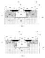
- FIG. 1 is a schematic illustration of a side view of an integrated semiconductor component and substrate, according to an illustrative embodiment.
- FIG. 2 is a schematic illustration of a side view of an integrated semiconductor component and substrate, according to an alternate illustrative embodiment.
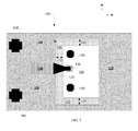
- FIG. 3 is a schematic illustration of a top view of an integrated semiconductor component and substrate, according to an illustrative embodiment.
- FIG. 4 is a flowchart of a method for integrating a semiconductor component and a substrate, according to an illustrative embodiment.
- FIGS. 1, 2 , and 3 are schematic illustrations of an electrical device100, according to illustrative embodiments.
- the electrical device 100 is depicted after integrating the components together as described below with respect to FIG. 4 .
- FIG. 1 is a side view (in the Z-X plane) of the electrical device 100 according to an illustrative embodiment.
- FIG. 2 is a side view (in the Z-X plane) of the electrical device 100 according to another illustrative embodiment.
- FIG. 3 is a top view (X-Y plane) of the embodiments of the electrical device 100 of FIGS. 1 and 2 .
- the electrical device 100 includes a semiconductor component 105 disposed in a cavity 108 formed in a layered substrate 109.
- the layered substrate 109 includes at least a first layer 110 disposed over a second layer 115.
- Active and passive semiconductor components 105 made of different materials (for example, GaN, GaAs, SiGe and Si), using different device technology (for example, p-HEMT, m-HEMT, SOI, and CMOS) and having different thickness are readily integrated into the layered substrate 109.
- the semiconductor components 105 include, for example, active and passive components such as high frequency discrete devices field effect transistors (FETs), monolithic microwave integrated circuits (MMICs), switches, attenuators, capacitors, resistors, inductors, and circulators.
- FETs high frequency discrete devices field effect transistors
- MMICs monolithic microwave integrated circuits
- switches attenuators, capacitors, resistors, inductors, and circulators.
- the first layer 110 is a low loss material adapted for fabricating a radio frequency (RF) matching network.
- the low loss material of the first layer 110 may be one of liquid crystal polymer (LCP) material, benzocyclobutene (BCB), or Teflon®.
- LCP liquid crystal polymer
- BCB benzocyclobutene
- Teflon® Teflon®
- the material of the first layer 110 has a dielectric constant and material thickness (along the Z-axis) that enables matching the width of the contact 135 on the semiconductor component 105 to the width of the electrical trace 130 on the first layer 110 in order to achieve the desired RF impedance.
- the first layer 110 is made of a low loss RF material, such as, for example, 1 mil thick LCP material having a loss tangent of 0.002 and a dielectric constant of 2.9.
- the electrical device 100 includes one or more cavities 108 of different depths formed in the layered substrate 109 for receiving one or more of the semiconductor components 105.
- the cavities 108 can be formed by various semiconductor fabrication techniques (e.g., etching or ablation).
- the depth of the cavity 108 (along the Z-axis) is determined based on thickness (along the Z-axis) of the semiconductor component 105 received therein and such that the top surface 134 of a contact 135 on the semiconductor component 105 is substantially coplanar with the top surface 129 of a trace 130 on the first layer 110 of the layered substrate 109. Aligning the top surface of the contact 135 with the top surface of the trace 130 accounts for any height difference between the contact 135 and network trace 130 and enables proper continuity in an electrical interconnect 125 patterned between the contact 135 and trace 130.
- the cavity 108 is formed in the layered substrate 109 such that the second layer 115 defines the cavity bottom 106.
- the top surface 117 of the second layer 115 defines the cavity bottom 106.
- an intermediate portion of the second layer 115 defines the cavity bottom 106.
- the semiconductor component 105 is 0.05 mm (2 mils) thick
- the first layer 110 is 0.025mm (1 mil) thick
- the cavity 108 extends 0.03 mm (1.2 mils) into the second layer 115.
- the depth of the cavity 108 therefore accommodates the thickness (along the Z-axis) of the semiconductor component 105 and also thickness (along the Z-axis) of attachment means 103 (e.g. adhesive or solder) disposed between the semiconductor component 105 and the cavity bottom 106 while still enabling coplanarity of the top surface 134 of a contact 135 on the semiconductor component 105 and the top surface 129 of a trace 130 on the first layer 110.
- the second layer 115 is formed from a highly thermally conductive material that forms the thermal plane for heat dissipation from the high power electrical device 105.
- the second layer 115 also forms a continuous ground plane for the RF signal of the electrical device 105 and the substrate of the first layer 110.
- the thermally dissipative material may be, for example, one of copper, copper alloys, such as molybdenum-copper and tungsten-copper, AlSiC, A1N, or silicon.
- an electrical interconnect 125 extends between an electrical trace 130 on the first layer 110 and an electrical contact 135 on the semiconductor component 105.
- FIG. 1 depicts a relatively thin deposition of the electrical interconnect 125 onto the electrical trace 130 and electrical contact 135.
- the electrical interconnect is plated to the same thickness on all surfaces (i.e., on the surfaces of the electrical trace 130, first layer 110, a dielectric material 120, and the electrical contact 135).
- the electrical interconnect 125 is fabricated to accommodate the variations in placement of the semiconductor component 105 without negatively affecting performance of the electrical interconnect 125, which forms a controlled impedance RF transmission line.
- Fabrication of the electrical interconnect 125 includes compensating for any misalignment between a contact 135 on the semiconductor component 105 and an electrical trace 130. Fabrication of the electrical interconnect 125 addresses not only the trajectory of the electrical interconnect 125 (i.e. the path the electrical interconnect takes over a surface) but also thickness and width such that the impedance is matched between the contact 135 and electrical trace 130 and RF loss is ultra low (e.g., between 0dB and 0.05dB at 100 GHz) at high frequency operation levels.
- the electrical interconnect 125 may be formed, for example, by direct writing techniques for depositing gold, silver, or copper conductors.
- the fabrication of the electrical interconnect 125 includes applying a photoresist to the entire top surface of the electrical device 100 and locally developing the photoresist with a low energy laser only in the areas in which each electrical interconnect 125 will be formed. The low energy laser, therefore, adaptively patterns each individual electrical interconnect 125 and accommodates variation in alignment (in the X-Y plane) between the one or more contacts 135 on the semiconductor component 105 and one or more corresponding electrical traces 130 on the first layer 110 of the layered substrate 109. Using a low energy laser exposure prevents material damage that otherwise could result from commonly-used laser ablation techniques.
- laser exposure includes a 355 nm laser producing 3.5 mw of power at a laser firing frequency of 30 KHz with a linear scan rate of 52 mm/sec and having a laser spot size of 16 microns.
- One embodiment includes employing two successive laser scans that expose seven microns of thick positive resist such as AZ-4620. The resist is then developed (removed) in suitable chemistry.
- the adaptive interconnect fabrication process involves applying a first layer of photoresist across the top surfaces of the layered substrate 109 and one or more semiconductor component 105 opening the photoresist with laser exposure and develop (i.e., removal) along the individual, unique path of each required electrical interconnect pattern and depositing a thin seed layer (e.g., 1000 angstroms thick) of conductive metal through sputtering.
- the seed layer covers at least the exposed area but, in embodiments, the seed layer may cover some or all of the remaining portion of the first layer of photoresist.
- the adaptive interconnect fabrication process then includes coating the electrical device 100 with a second layer of photoresist, reopening the photoresist with the low energy laser along the individual, unique path of each of the electrical interconnects 125 (i.e., exposing the conductive seed layer) and finally electroplating the conductive seed layer to form the completed electrical interconnects 125 that accommodate for variation in alignment between each electrical conductor 135 and electrical trace 130.
- the first and second layers of photoresist and any unplated portions of the seed layer applied to the first layer of photoresist are removed from all surfaces of the electrical device 100 surrounding the plated one or more electrical interconnects 125. This process leaves each adaptively patterned electrical interconnect 125 extending between the electrical contact 135 on the semiconductor component 105 and the electrical trace 130 on the layered substrate 109.
- the electrical interconnect 125 may also be formed by directly writing with copper, gold or silver conductor ink.
- Common RF circuit design tools such as, for example, Agilent® advanced design system and Ansoft® HFSS, may be employed to determine the width of the electrical interconnect 125 for a given thickness of an electrical trace 130.
- the method of forming the electrical interconnect 125 comprises using a software algorithm to locate the position of fiducials 140 on the semiconductor component relative to fiducials 145 on the first layer 115 and calculating a profile (i.e., width and taper) of the electrical interconnect 125 based on prior knowledge of RF properties provided by the RF circuit design tool.
- Using a low energy laser to expose and develop out photoresist enables local exposure and localized adaptive patterning for each electrical interconnect 125.
- This technique accounts for small variations not accounted for in standard wafer mask techniques that treat all traces on a wafer similarly and without consideration to individualized variations in alignment between each electrical contact 135 and electrical trace 130. This technique therefore accommodates variations in alignment between the electrical contacts 135 and electrical traces 130 while providing an effective controlled impedance RF transmission line.
- the semiconductor component 105 is disposed in the cavity 108 such that the electrical contact 135 on the top surface 107 of the semiconductor component 105 is substantially aligned (along the Z-axis) with the electrical trace 130 on the first layer 115 of the layered substrate 109 prior to formation of the electrical interconnect 125.
- the trajectory of the electrical interconnect 125 in the X-Y plane is based on the relative positions of at least one fixed fiducial 145 on the first layer 110 and at least one fixed fiducial 140 on the semiconductor component 105.
- the position of the electrical trace 130 on the first layer 110 is fixed relative to the at least one fixed fiducial 145 on the first layer 110, and the position of the electrical contact 135 on the semiconductor component 105 is fixed relative to the at least one fixed fiducial 140 on the semiconductor component 105.
- the electrical device 100 includes a gap 122 between the semiconductor component 105 and walls 111 of the cavity 108.
- the gap 122 is approximately equal between all sides of the device and the adjacent, corresponding walls 111 of the cavity 108.
- the gap 122 is between 0-40 microns, and in some illustrative embodiments, the gap 122 between the semiconductor component 105 and the walls 111 of the cavity 108 is between 25-35 microns.
- the gap 122 between the semiconductor component 105 and the walls 111 of the cavity 108 is filled with a dielectric material 120 that is a low shrinkage (for example 12% or less), low viscosity material that efficiently fills the gap 122.
- the dielectric material has a low curing temperature (for example, approximately 200 degrees Celsius).
- the dielectric material 120 is low loss and has a dielectric constant matching that of the material of the first layer 110.
- the dielectric material 120 filling the gap 122 is one of Intervia 8023-10, BCB, or Teflon® and has a dielectric constant of approximately 3.0.
- the dielectric material 120 fills the gap 122 such that a top surface 121 of the dielectric material 120 is substantially coplanar with the top surface 107 of the semiconductor component 105 and the top surface 113 of the first layer 110.
- the dielectric material 120 is spin coated across the entire electrical device 100 and selectively removed by photolithography, leaving dielectric material 120 only in the gap 122.
- the dielectric material 120 in the gap 122 is then cured such that the top surface 121 of the dielectric material 120 is coplanar with the top surface 113 of the first layer 110.
- the electrical interconnect 125 is formed across the coplanar surfaces of the first layer 110, dielectric material 120 and semiconductor component 105 to achieve a matched impedance between the contact 135 and trace 130.
- the electrical interconnect 125 could be an impedance transition member of, for example, 50 ohms or 70 ohms, to match the layered substrate 109 electrical characteristics with those of the semiconductor component 105 and create an RF transmission line.
- the electrical interconnect 125 has a RF signal loss of between 0 dB and 0.05 dB at 100 GHz, and is 3 to 5 microns thick as measured from top to bottom (i.e., along the Z-axis).
- the dielectric material 120 therefore eliminates any discontinuity in RF transmission lines associated with existing wire/ribbon bonds and flip chip integration techniques.
- the dielectric material 120 filling the gap 122 around the semiconductor component 105 eliminates any discontinuity in underlying support structure, and enables a continuous micro-strip interconnection formed by the electrical interconnect 125 adaptively patterned on the semiconductor component 105, first layer 110 and dielectric material 120 between the contact 135 and trace 130.
- an adhesive is applied to the cavity bottom 106 in dispensable paste or solid film form.
- Suitable adhesives have a cure temperature less than about 200 degrees Celsius and may comprise any one or more of the following functions: isotropically or anisotropically electrically conducting, electrically insulating, thermally conducting, strongly adhering to noble or non-noble metallizations, moisture resistant, chemically resistant, low outgassing, thermally stable, and flexible or stress absorbing.
- Suitable adhesives are, for example, one-component, silver or silver alloy-filled pastes and films that are isotropically electrically conducting, thermally conducting, stress absorbing, strongly adhering to gold metallization, and/or which cure at less than about 150 degrees Celsius.
- Preferred paste adhesives also exhibit viscosity below 60,000 cps at 25 degrees Celsius, a thixotropic index between about 2 and 5, thermal conductivity greater than about 1.5 W-m/K, low resin bleed, high purity, good wetting on gold metallization, shear strength greater than about 17MPa (2,500 psi) at 25 degrees Celsius, low ionic content, and volume resistivity less than 5x10 -4 ohm-cm.
- Suitable film adhesives also exhibit preform thickness less than 0.08mm (0.003in), thermal conductivity greater than about 1.5 W-m/K, low resin bleed, high purity, good adhesion on gold metallization, shear strength greater than about 17MPa (2,500 psi) at 25 degrees Celsius, low ionic content, volume resistivity less than 5x10 -4 ohm-cm, and application pressure less than about 103kPa (15 psi).
- solders are applied to the cavity bottom 106 in a fluxed paste form or as a non-fluxed solid preform.
- Suitable solder formulations are eutectic and non-eutectic alloys with a liquidus temperature below about 250 degrees Celsius and a solidus temperature above about 150 degrees Celsius.
- Suitable alloys include tin-lead, lead-free, and specialty (non-tin/lead) formulations, as defined in IPC/EIA J-STD-006, Requirements for Electronic Grade Solder Alloys and Fluxed and Non-Fluxed Solid Solders for Electronic Soldering Applications.
- Preferred solder alloys have a solidus above about 170 degrees Celsius and a liquidus below about 230 degrees Celsius.
- Preferred tin-lead formulations include, for example: Sn63Pb37, Sn62Pb36Ag2, Sn70Pb30, Sn90Pb10, Sn50Pb48.5Cu1.5, Sn50Pb50, Sn50Pb50Sb0.4, In20Sn54Pb26, Sn60Pb37.5Bi2.5, Sn60Pb38Cu2, Sn60Pb40, Sn60Pb40Sb0.4, Sn62Pb36Ag02Sb0.4, Sn63Pb37Sb0.4, and Sn70Pb30Sb0.4.
- Lead-free formulations include, for example: Sn96.3Ag3.7, Sn95.5Ag3.8Cu0.7, Sn95.8Ag3.5Cu0.7, Sn95Ag4Cd1, Sn96Ag2.5Cu0.5Bi1, Sn96.3Ag2.5Cu0.7Sb0.5, Sn96.4Ag3.2Cu0.4, Sn96.5Ag3.5, Sn99.3Cu0.7.
- Preferred specialty alloys include: In40Pb60, In50Pb50, and In60Pb40.
- FIG. 4 is a flowchart of a method for integrating a semiconductor component with a layered substrate to create a high frequency electrical device (e.g., the semiconductor component 105 and layered substrate 109 of the device of FIG. 1 ).
- the method produces a mm-wave frequency electrical device and in another embodiment, the method produces an electrical device that operates at over 100GHz.
- the electrical device can include active and passive semiconductor components made of different materials (for example, GaN, GaAs, SiGe and Si), different device technology (for example, p-HEMT, m-HEMT, SOI, CMOS and others) and different thickness that are heterogeneously integrated into the layered substrate.
- the method includes forming S205 a cavity in a layered substrate (e.g., cavity 108 in layered substrate 109 of FIG. 1 ), the layered substrate includes a first layer disposed over a second layer such that the second layer defines the cavity bottom.
- the method includes disposing S210 a semiconductor component in the cavity such that a top surface of the conductor pad in the semiconductor component is substantially coplanar with the top surface of the conductor trace on the first layer of the layered substrate.
- multiple types of semiconductor components, active and passive, and multiple cavities are heterogeneously integrated within the same layered substrate.
- the method includes locating S215 at least one fixed fiducial on the first layer, and locating S220 at least one fixed fiducial on the semiconductor component.
- the method includes forming S225 an electrical interconnect between an electrical trace on the first layer and an electrical contact on the semiconductor component based on the relative positions of the at least one fixed fiducial on the first layer and the at least one fixed fiducial on the semiconductor component, wherein the position of the electrical trace on the first layer is fixed relative to the at least one fixed fiducial on the first layer and the position of the electrical contact on the semiconductor component is fixed relative to the at least one fixed fiducial on the semiconductor component.
- the electrical trace may be formed, for example, by a highly precise conductor direct write process or laser exposure of photoresist, electroplating and etching processes.
- the step of forming S205 the cavity includes sizing S207 the cavity such that a gap exists between the semiconductor component and walls of the cavity. It should be noted that sizing S207 the cavity size can occur prior to forming the cavity in S205. In some embodiments, forming S205 the cavity requires forming portions of the cavity independently in the first layer and second layer of the layered substrate. For example, with regard to the embodiment of FIG. 2 , the cavity 108 may be etched in layer 115 and then the cavity formed in layer 110 after it is deposited on layer 115.
- the gap between the semiconductor component and the walls of the cavity is 0-40 microns. In another embodiment, the gap between the semiconductor component and the walls of the cavity is 25-35 microns. In one embodiment, the method further includes filling S214 the gap between the semiconductor component and the walls of the cavity with dielectric material such that a top surface of a trace on the dielectric material is substantially coplanar with the top surface of a contact on the semiconductor component and the top surface of the first layer. In some embodiments, the method includes applying S208 an adhesive between the cavity bottom and the semiconductor component, and in other embodiments, the method includes applying S208 solder between the cavity bottom and the semiconductor component.
- the method includes adaptively patterning the electrical interconnect onto the coplanar top surfaces of the first layer, dielectric fill and semiconductor component such that impedance is matched between the components and a low loss, high frequency RF transmission line is formed over a continuous solid surface of low dielectric constant.
- the electrical interconnect has a RF signal loss of only between 0dB and 0.05dB at 100GHz.
- the electrical interconnect is patterned on the electrical device using local laser exposure of photoresist and electroplating techniques, and in other embodiments, the electrical interconnect is dispensed using a pen, a stamping process, or a direct write process that direct writes conductors made of gold, silver, or copper.
- the method employs using a patterning tool for locating S215 the at least one fixed fiducial on the semiconductor component and locating S220 at least one fixed fiducial on the first layer.
- the method prior to disposing the semiconductor component into the cavity, includes substantially aligning S212 the contacts on the semiconductor component with an electrical trace on the first layer of the layered substrate. This further improves the accuracy and efficiency of forming 225 the electrical interconnect.
- the tool employs a software means that adjusts the pattern of the electrical interconnect to achieve proper impedance matching while compensating for any variation in interconnect length between contacts on the semiconductor component and corresponding network traces on the first layer of the layered substrate.
- the embodiments include stretching, compressing, translating and/or rotating the pattern for the electrical interconnect as needed to accommodate the variation in placement of the semiconductor component within the cavity and relative to the traces on the layered substrate and obtaining optimum high frequency electrical performance (i.e., performance with little to no RF loss, such as 0dB to 0.05dB at 100GHz).
- adjusting the pattern can include translating the location of the electrical interconnect in the X-Y plane and/or stretching the electrical interconnect to increase length and/or width to connect the contacts and traces and match impedance between those elements.
- the method therefore accommodates placement variation of the semiconductor component while matching impedances between the contacts and traces to ensure minimal or no RF loss at high operational frequencies.
- the patterning tool patterns the electrical interconnect to fit the actual transition between the contact and trace.
- the method therefore integrates semiconductor components through ultra low loss adaptive electrical interconnections by recognizing the location of a semiconductor component and patterning a high precision conductor (i.e., electrical interconnect) between the semiconductor component and a network trace formed on the layered substrate.
- Comprise, include, and/or plural forms of each are open ended and include the listed parts and can include additional parts that are not listed. And/or is open ended and includes one or more of the listed parts and combinations of the listed parts.
Landscapes
- Engineering & Computer Science (AREA)
- Microelectronics & Electronic Packaging (AREA)
- Manufacturing & Machinery (AREA)
- Internal Circuitry In Semiconductor Integrated Circuit Devices (AREA)
- Wire Bonding (AREA)
Abstract
Description
- The currently described invention relates to systems and methods for integrating semiconductor components, including active and passive devices, with a substrate.
- Semiconductor integration methods typically involve connecting active and/or passive elements with passive circuitry via wire or ribbon bonds or flip chip bumps that manifest parasitic behavior at higher frequencies (i.e., at or greater than 10 GHz). In these integration methods, discontinuities in RF (radio frequency) transmission lines are caused by discontinuities in dielectric properties of underlying material and air gaps between bridged materials (e.g., discontinuity between the dielectric of a substrate material to air). The ribbon bond, flip chip technique compromises performance in high radio frequency applications. Additionally, placement inaccuracies between a semiconductor component and a substrate are typically overcome by increasing landing pad dimensions, which results in a substantial increase in radio frequency signal loss at the transition between the semiconductor component and the substrate. These placement inaccuracies also result in requiring a greater pitch between components on the substrate, and increased size and associated cost of the substrate and components.
- A need therefore exists for improved methods and systems for integrating semiconductor components with a substrate that compensates for placement inaccuracies without causing performance degradation at high radio frequencies, increased pitch between components, or an increase in component size.
- One embodiment is a method for integrating a semiconductor component with a layered substrate. The method includes forming a cavity in a layered substrate. The layered substrate includes a first layer disposed over a second layer of the layered substrate such that the second layer defines the cavity bottom. The method also includes disposing a semiconductor component in the cavity such that a top surface of an electrical contact on the semiconductor component is substantially coplanar with the top surface of an electrical trace on the first layer of the layered substrate. The method also includes locating at least one fixed fiducial on the first layer. The method also includes locating at least one fixed fiducial on the semiconductor component. The method also includes forming an electrical interconnect between the electrical trace on the first layer and the electrical contact on the semiconductor component based on the relative positions of the at least one fixed fiducial on the first layer and the at least one fixed fiducial on the semiconductor component, wherein the position of the electrical trace on the first layer is fixed relative to the at least one fixed fiducial on the first layer and the position of the electrical contact on the semiconductor component is fixed relative to the at least one fixed fiducial on the semiconductor component.
- In some embodiments, the step of forming the cavity includes sizing the cavity such that a gap of 0-40 microns exists between the semiconductor component and walls of the cavity. In some embodiments, a gap of 25-35 microns exists between the semiconductor component and the walls of the cavity. In some embodiments, the method includes filling the gap between the semiconductor and the walls of the cavity with dielectric material such that a top surface of the dielectric material is substantially coplanar with the top surface of the semiconductor component and the top surface of the first layer. In some embodiments, the method optionally includes applying an adhesive between the cavity bottom and the semiconductor component. In some embodiments, the method optionally includes applying a solder between the cavity bottom and the semiconductor component. In some embodiments, the method includes disposing the semiconductor component in the cavity such that the electrical contact on the top surface of the semiconductor component is substantially aligned with the electrical trace on the first layer of the layered substrate, wherein alignment includes locating the relative positions of the at least one fixed fiducial on the first layer and the at least one fixed fiducial on the semiconductor component.
- In some embodiments, the method includes patterning the electrical trace to compensate for variation in interconnect length between one or more contacts on the semiconductor component and one or more corresponding electrical traces. In one embodiment, the method includes at least one of stretching, compressing, translating or rotating the electrical trace pattern to accommodate for variation in placement of the semiconductor component within the cavity.
- In some embodiments, the method includes using a low energy laser to locally develop a photoresist applied to the electrical device, thereby adaptively patterning each individual electrical interconnect extending between one of the one or more contacts and a corresponding one of the one or more electrical traces, thereby accommodating misalignment. In some embodiments, the low energy laser is a 355 nm laser producing 3.5 mw of power at a laser firing frequency of 30 KHz with a linear scan rate of 52 mm/sec and having a laser spot size of 16 microns.
- In one embodiment, the method includes forming the electrical interconnect using one of a pen, a stamping process, or a direct write process that direct writes conductors made of gold, silver, or copper.
- In some embodiments, the method includes coating a first layer of photoresist across the top surfaces of the first layer and semiconductor component, opening the first layer of photoresist with laser exposure and development along the electrical interconnect pattern. The method includes depositing a conductive seed layer at least along the electrical interconnect pattern opened in the first layer of photoresist, and coating a second layer of photoresist across the top surfaces of the first layer, semiconductor component, and seed layer. The method includes opening the second layer of photoresist with laser exposure and development along the electrical interconnect pattern, electroplating the seed layer along the electrical interconnect pattern and removing the first layer of photoresist, second layer of photoresist, and unplated seed layer disposed therebetween, if present.
- In some embodiments, the low energy laser is a 355 nm laser producing 3.5 mw of power at a laser firing frequency of 30 KHz with a linear scan rate of 52 mm/sec and having a laser spot size of 16 microns.
- Another embodiment is an electrical device. The electrical device includes a layered substrate comprising a first layer disposed over a second layer of the layered substrate. The electrical device also includes a cavity formed in the layered substrate such that the second layer defines the cavity bottom, and a semiconductor component disposed in the cavity such that a top surface of an electrical contact on the semiconductor component is substantially coplanar with a top surface of an electrical trace on the first layer of the layered substrate. The electrical device also includes an electrical interconnect extending between the electrical trace on the first layer and the electrical contact on the semiconductor component. The path of the electrical interconnect is based on relative positions of at least one fixed fiducial on the first layer and at least one fixed fiducial on the semiconductor component. The position of the electrical trace on the first layer is fixed relative to the at least one fixed fiducial on the first layer, and the position of the electrical contact on the semiconductor component is fixed relative to the at least one fixed fiducial on the semiconductor component.
- In some embodiments, the cavity is formed such that a gap of 0-40 microns exists between the semiconductor component and walls of the cavity. In some embodiments, the electrical device includes a fill of dielectric material in the gap between the semiconductor and the walls of the cavity, and the top surface of the dielectric material is substantially coplanar with the top surface of the semiconductor component and the top surface of the first layer. In some embodiments, the semiconductor component is placed in the cavity such that the electrical contact on the top surface of the semiconductor component is substantially aligned with the electrical trace on the first layer of the layered substrate based on the relative positions of the at least one fixed fiducial on the first layer and the at least one fixed fiducial on the semiconductor component.
- Other aspects and advantages of the current invention will become apparent from the following detailed description, taken in conjunction with the accompanying drawings, illustrating the principles of the invention by way of example only.
- The foregoing features of various embodiments of the invention will be more readily understood by reference to the following detailed descriptions in the accompanying drawings, in which:
-
FIG. 1 is a schematic illustration of a side view of an integrated semiconductor component and substrate, according to an illustrative embodiment. -
FIG. 2 is a schematic illustration of a side view of an integrated semiconductor component and substrate, according to an alternate illustrative embodiment. -
FIG. 3 is a schematic illustration of a top view of an integrated semiconductor component and substrate, according to an illustrative embodiment. -
FIG. 4 is a flowchart of a method for integrating a semiconductor component and a substrate, according to an illustrative embodiment. -
FIGS. 1, 2 , and3 are schematic illustrations of an electrical device100, according to illustrative embodiments. Theelectrical device 100 is depicted after integrating the components together as described below with respect toFIG. 4 .FIG. 1 is a side view (in the Z-X plane) of theelectrical device 100 according to an illustrative embodiment.FIG. 2 is a side view (in the Z-X plane) of theelectrical device 100 according to another illustrative embodiment.FIG. 3 is a top view (X-Y plane) of the embodiments of theelectrical device 100 ofFIGS. 1 and 2 . Theelectrical device 100 includes asemiconductor component 105 disposed in acavity 108 formed in alayered substrate 109. Thelayered substrate 109 includes at least afirst layer 110 disposed over asecond layer 115. Active andpassive semiconductor components 105 made of different materials (for example, GaN, GaAs, SiGe and Si), using different device technology (for example, p-HEMT, m-HEMT, SOI, and CMOS) and having different thickness are readily integrated into thelayered substrate 109. Thesemiconductor components 105 include, for example, active and passive components such as high frequency discrete devices field effect transistors (FETs), monolithic microwave integrated circuits (MMICs), switches, attenuators, capacitors, resistors, inductors, and circulators. - In some embodiments, the
first layer 110 is a low loss material adapted for fabricating a radio frequency (RF) matching network. For example, the low loss material of thefirst layer 110 may be one of liquid crystal polymer (LCP) material, benzocyclobutene (BCB), or Teflon®. The material of thefirst layer 110 has a dielectric constant and material thickness (along the Z-axis) that enables matching the width of thecontact 135 on thesemiconductor component 105 to the width of theelectrical trace 130 on thefirst layer 110 in order to achieve the desired RF impedance. In one embodiment, thefirst layer 110 is made of a low loss RF material, such as, for example, 1 mil thick LCP material having a loss tangent of 0.002 and a dielectric constant of 2.9. - Referring to the illustrative embodiments of
FIGS. 1 and 2 , theelectrical device 100 includes one ormore cavities 108 of different depths formed in thelayered substrate 109 for receiving one or more of thesemiconductor components 105. In some embodiments, multiple types of components, active and passive, and multiple cavities are heterogeneously integrated within the same layered substrate. Thecavities 108 can be formed by various semiconductor fabrication techniques (e.g., etching or ablation). The depth of the cavity 108 (along the Z-axis) is determined based on thickness (along the Z-axis) of thesemiconductor component 105 received therein and such that thetop surface 134 of acontact 135 on thesemiconductor component 105 is substantially coplanar with thetop surface 129 of atrace 130 on thefirst layer 110 of thelayered substrate 109. Aligning the top surface of thecontact 135 with the top surface of thetrace 130 accounts for any height difference between thecontact 135 andnetwork trace 130 and enables proper continuity in anelectrical interconnect 125 patterned between thecontact 135 andtrace 130. - The
cavity 108 is formed in thelayered substrate 109 such that thesecond layer 115 defines thecavity bottom 106. Referring toFIG. 1 , thetop surface 117 of thesecond layer 115 defines thecavity bottom 106. Alternatively, as depicted inFIG. 2 , an intermediate portion of thesecond layer 115 defines thecavity bottom 106. In one embodiment, thesemiconductor component 105 is 0.05 mm (2 mils) thick, thefirst layer 110 is 0.025mm (1 mil) thick and thecavity 108 extends 0.03 mm (1.2 mils) into thesecond layer 115. The depth of thecavity 108 therefore accommodates the thickness (along the Z-axis) of thesemiconductor component 105 and also thickness (along the Z-axis) of attachment means 103 (e.g. adhesive or solder) disposed between thesemiconductor component 105 and thecavity bottom 106 while still enabling coplanarity of thetop surface 134 of acontact 135 on thesemiconductor component 105 and thetop surface 129 of atrace 130 on thefirst layer 110. - In some embodiments, the
second layer 115 is formed from a highly thermally conductive material that forms the thermal plane for heat dissipation from the high powerelectrical device 105. Thesecond layer 115 also forms a continuous ground plane for the RF signal of theelectrical device 105 and the substrate of thefirst layer 110. The thermally dissipative material may be, for example, one of copper, copper alloys, such as molybdenum-copper and tungsten-copper, AlSiC, A1N, or silicon. - With the
semiconductor component 105 situated in thecavity 108, anelectrical interconnect 125 extends between anelectrical trace 130 on thefirst layer 110 and anelectrical contact 135 on thesemiconductor component 105.FIG. 1 depicts a relatively thin deposition of theelectrical interconnect 125 onto theelectrical trace 130 andelectrical contact 135. In some embodiments, the electrical interconnect is plated to the same thickness on all surfaces (i.e., on the surfaces of theelectrical trace 130,first layer 110, adielectric material 120, and the electrical contact 135). Theelectrical interconnect 125 is fabricated to accommodate the variations in placement of thesemiconductor component 105 without negatively affecting performance of theelectrical interconnect 125, which forms a controlled impedance RF transmission line. Fabrication of theelectrical interconnect 125 includes compensating for any misalignment between acontact 135 on thesemiconductor component 105 and anelectrical trace 130. Fabrication of theelectrical interconnect 125 addresses not only the trajectory of the electrical interconnect 125 (i.e. the path the electrical interconnect takes over a surface) but also thickness and width such that the impedance is matched between thecontact 135 andelectrical trace 130 and RF loss is ultra low (e.g., between 0dB and 0.05dB at 100 GHz) at high frequency operation levels. - In some embodiments, the
electrical interconnect 125 may be formed, for example, by direct writing techniques for depositing gold, silver, or copper conductors. In some embodiments, the fabrication of theelectrical interconnect 125 includes applying a photoresist to the entire top surface of theelectrical device 100 and locally developing the photoresist with a low energy laser only in the areas in which eachelectrical interconnect 125 will be formed. The low energy laser, therefore, adaptively patterns each individualelectrical interconnect 125 and accommodates variation in alignment (in the X-Y plane) between the one ormore contacts 135 on thesemiconductor component 105 and one or more correspondingelectrical traces 130 on thefirst layer 110 of thelayered substrate 109. Using a low energy laser exposure prevents material damage that otherwise could result from commonly-used laser ablation techniques. For example, in one embodiment, laser exposure includes a 355 nm laser producing 3.5 mw of power at a laser firing frequency of 30 KHz with a linear scan rate of 52 mm/sec and having a laser spot size of 16 microns. One embodiment includes employing two successive laser scans that expose seven microns of thick positive resist such as AZ-4620. The resist is then developed (removed) in suitable chemistry. - In one embodiment, the adaptive interconnect fabrication process involves applying a first layer of photoresist across the top surfaces of the
layered substrate 109 and one ormore semiconductor component 105 opening the photoresist with laser exposure and develop (i.e., removal) along the individual, unique path of each required electrical interconnect pattern and depositing a thin seed layer (e.g., 1000 angstroms thick) of conductive metal through sputtering. The seed layer covers at least the exposed area but, in embodiments, the seed layer may cover some or all of the remaining portion of the first layer of photoresist. The adaptive interconnect fabrication process then includes coating theelectrical device 100 with a second layer of photoresist, reopening the photoresist with the low energy laser along the individual, unique path of each of the electrical interconnects 125 (i.e., exposing the conductive seed layer) and finally electroplating the conductive seed layer to form the completedelectrical interconnects 125 that accommodate for variation in alignment between eachelectrical conductor 135 andelectrical trace 130. Following the electroplating process, the first and second layers of photoresist and any unplated portions of the seed layer applied to the first layer of photoresist are removed from all surfaces of theelectrical device 100 surrounding the plated one or moreelectrical interconnects 125. This process leaves each adaptively patternedelectrical interconnect 125 extending between theelectrical contact 135 on thesemiconductor component 105 and theelectrical trace 130 on thelayered substrate 109. - In other embodiments, the
electrical interconnect 125 may also be formed by directly writing with copper, gold or silver conductor ink. Common RF circuit design tools such as, for example, Agilent® advanced design system and Ansoft® HFSS, may be employed to determine the width of theelectrical interconnect 125 for a given thickness of anelectrical trace 130. In embodiments, the method of forming theelectrical interconnect 125 comprises using a software algorithm to locate the position offiducials 140 on the semiconductor component relative to fiducials 145 on thefirst layer 115 and calculating a profile (i.e., width and taper) of theelectrical interconnect 125 based on prior knowledge of RF properties provided by the RF circuit design tool. Using a low energy laser to expose and develop out photoresist enables local exposure and localized adaptive patterning for eachelectrical interconnect 125. This technique accounts for small variations not accounted for in standard wafer mask techniques that treat all traces on a wafer similarly and without consideration to individualized variations in alignment between eachelectrical contact 135 andelectrical trace 130. This technique therefore accommodates variations in alignment between theelectrical contacts 135 andelectrical traces 130 while providing an effective controlled impedance RF transmission line. - In some illustrative embodiments, the
semiconductor component 105 is disposed in thecavity 108 such that theelectrical contact 135 on thetop surface 107 of thesemiconductor component 105 is substantially aligned (along the Z-axis) with theelectrical trace 130 on thefirst layer 115 of thelayered substrate 109 prior to formation of theelectrical interconnect 125. - Referring to
FIG. 3 , the trajectory of theelectrical interconnect 125 in the X-Y plane is based on the relative positions of at least one fixed fiducial 145 on thefirst layer 110 and at least one fixed fiducial 140 on thesemiconductor component 105. The position of theelectrical trace 130 on thefirst layer 110 is fixed relative to the at least one fixed fiducial 145 on thefirst layer 110, and the position of theelectrical contact 135 on thesemiconductor component 105 is fixed relative to the at least one fixed fiducial 140 on thesemiconductor component 105. - The
electrical device 100 includes agap 122 between thesemiconductor component 105 and walls 111 of thecavity 108. In the illustrative embodiment shown inFIG. 3 , thegap 122 is approximately equal between all sides of the device and the adjacent, corresponding walls 111 of thecavity 108. In some embodiments, thegap 122 is between 0-40 microns, and in some illustrative embodiments, thegap 122 between thesemiconductor component 105 and the walls 111 of thecavity 108 is between 25-35 microns. - The
gap 122 between thesemiconductor component 105 and the walls 111 of thecavity 108 is filled with adielectric material 120 that is a low shrinkage (for example 12% or less), low viscosity material that efficiently fills thegap 122. The dielectric material has a low curing temperature (for example, approximately 200 degrees Celsius). Thedielectric material 120 is low loss and has a dielectric constant matching that of the material of thefirst layer 110. For example, in one embodiment, thedielectric material 120 filling thegap 122 is one of Intervia 8023-10, BCB, or Teflon® and has a dielectric constant of approximately 3.0. - In some embodiments, the
dielectric material 120 fills thegap 122 such that atop surface 121 of thedielectric material 120 is substantially coplanar with thetop surface 107 of thesemiconductor component 105 and thetop surface 113 of thefirst layer 110. In some embodiments, thedielectric material 120 is spin coated across the entireelectrical device 100 and selectively removed by photolithography, leavingdielectric material 120 only in thegap 122. Thedielectric material 120 in thegap 122 is then cured such that thetop surface 121 of thedielectric material 120 is coplanar with thetop surface 113 of thefirst layer 110. Theelectrical interconnect 125 is formed across the coplanar surfaces of thefirst layer 110,dielectric material 120 andsemiconductor component 105 to achieve a matched impedance between thecontact 135 andtrace 130. For example, in embodiments, theelectrical interconnect 125 could be an impedance transition member of, for example, 50 ohms or 70 ohms, to match thelayered substrate 109 electrical characteristics with those of thesemiconductor component 105 and create an RF transmission line. In some embodiments, theelectrical interconnect 125 has a RF signal loss of between 0 dB and 0.05 dB at 100 GHz, and is 3 to 5 microns thick as measured from top to bottom (i.e., along the Z-axis). Thedielectric material 120 therefore eliminates any discontinuity in RF transmission lines associated with existing wire/ribbon bonds and flip chip integration techniques. Thedielectric material 120 filling thegap 122 around thesemiconductor component 105 eliminates any discontinuity in underlying support structure, and enables a continuous micro-strip interconnection formed by theelectrical interconnect 125 adaptively patterned on thesemiconductor component 105,first layer 110 anddielectric material 120 between thecontact 135 andtrace 130. - In some illustrative embodiments, an adhesive is applied to the
cavity bottom 106 in dispensable paste or solid film form. Suitable adhesives have a cure temperature less than about 200 degrees Celsius and may comprise any one or more of the following functions: isotropically or anisotropically electrically conducting, electrically insulating, thermally conducting, strongly adhering to noble or non-noble metallizations, moisture resistant, chemically resistant, low outgassing, thermally stable, and flexible or stress absorbing. Suitable adhesives are, for example, one-component, silver or silver alloy-filled pastes and films that are isotropically electrically conducting, thermally conducting, stress absorbing, strongly adhering to gold metallization, and/or which cure at less than about 150 degrees Celsius. Preferred paste adhesives also exhibit viscosity below 60,000 cps at 25 degrees Celsius, a thixotropic index between about 2 and 5, thermal conductivity greater than about 1.5 W-m/K, low resin bleed, high purity, good wetting on gold metallization, shear strength greater than about 17MPa (2,500 psi) at 25 degrees Celsius, low ionic content, and volume resistivity less than 5x10⁻⁴ ohm-cm. Suitable film adhesives also exhibit preform thickness less than 0.08mm (0.003in), thermal conductivity greater than about 1.5 W-m/K, low resin bleed, high purity, good adhesion on gold metallization, shear strength greater than about 17MPa (2,500 psi) at 25 degrees Celsius, low ionic content, volume resistivity less than 5x10⁻⁴ ohm-cm, and application pressure less than about 103kPa (15 psi). - In some embodiments, solders are applied to the
cavity bottom 106 in a fluxed paste form or as a non-fluxed solid preform. Suitable solder formulations are eutectic and non-eutectic alloys with a liquidus temperature below about 250 degrees Celsius and a solidus temperature above about 150 degrees Celsius. Suitable alloys include tin-lead, lead-free, and specialty (non-tin/lead) formulations, as defined in IPC/EIA J-STD-006, Requirements for Electronic Grade Solder Alloys and Fluxed and Non-Fluxed Solid Solders for Electronic Soldering Applications. Preferred solder alloys have a solidus above about 170 degrees Celsius and a liquidus below about 230 degrees Celsius. Preferred tin-lead formulations include, for example: Sn63Pb37, Sn62Pb36Ag2, Sn70Pb30, Sn90Pb10, Sn50Pb48.5Cu1.5, Sn50Pb50, Sn50Pb50Sb0.4, In20Sn54Pb26, Sn60Pb37.5Bi2.5, Sn60Pb38Cu2, Sn60Pb40, Sn60Pb40Sb0.4, Sn62Pb36Ag02Sb0.4, Sn63Pb37Sb0.4, and Sn70Pb30Sb0.4. Lead-free formulations include, for example: Sn96.3Ag3.7, Sn95.5Ag3.8Cu0.7, Sn95.8Ag3.5Cu0.7, Sn95Ag4Cd1, Sn96Ag2.5Cu0.5Bi1, Sn96.3Ag2.5Cu0.7Sb0.5, Sn96.4Ag3.2Cu0.4, Sn96.5Ag3.5, Sn99.3Cu0.7. Preferred specialty alloys include: In40Pb60, In50Pb50, and In60Pb40. -
FIG. 4 is a flowchart of a method for integrating a semiconductor component with a layered substrate to create a high frequency electrical device (e.g., thesemiconductor component 105 andlayered substrate 109 of the device ofFIG. 1 ). In one embodiment, the method produces a mm-wave frequency electrical device and in another embodiment, the method produces an electrical device that operates at over 100GHz. As indicated above, the electrical device can include active and passive semiconductor components made of different materials (for example, GaN, GaAs, SiGe and Si), different device technology (for example, p-HEMT, m-HEMT, SOI, CMOS and others) and different thickness that are heterogeneously integrated into the layered substrate. - The method includes forming S205 a cavity in a layered substrate (e.g.,
cavity 108 inlayered substrate 109 ofFIG. 1 ), the layered substrate includes a first layer disposed over a second layer such that the second layer defines the cavity bottom. The method includes disposing S210 a semiconductor component in the cavity such that a top surface of the conductor pad in the semiconductor component is substantially coplanar with the top surface of the conductor trace on the first layer of the layered substrate. In some embodiments, multiple types of semiconductor components, active and passive, and multiple cavities are heterogeneously integrated within the same layered substrate. The method includes locating S215 at least one fixed fiducial on the first layer, and locating S220 at least one fixed fiducial on the semiconductor component. The method includes forming S225 an electrical interconnect between an electrical trace on the first layer and an electrical contact on the semiconductor component based on the relative positions of the at least one fixed fiducial on the first layer and the at least one fixed fiducial on the semiconductor component, wherein the position of the electrical trace on the first layer is fixed relative to the at least one fixed fiducial on the first layer and the position of the electrical contact on the semiconductor component is fixed relative to the at least one fixed fiducial on the semiconductor component. The electrical trace may be formed, for example, by a highly precise conductor direct write process or laser exposure of photoresist, electroplating and etching processes. - In one embodiment, the step of forming S205 the cavity includes sizing S207 the cavity such that a gap exists between the semiconductor component and walls of the cavity. It should be noted that sizing S207 the cavity size can occur prior to forming the cavity in S205. In some embodiments, forming S205 the cavity requires forming portions of the cavity independently in the first layer and second layer of the layered substrate. For example, with regard to the embodiment of
FIG. 2 , thecavity 108 may be etched inlayer 115 and then the cavity formed inlayer 110 after it is deposited onlayer 115. - In one embodiment, the gap between the semiconductor component and the walls of the cavity is 0-40 microns. In another embodiment, the gap between the semiconductor component and the walls of the cavity is 25-35 microns. In one embodiment, the method further includes filling S214 the gap between the semiconductor component and the walls of the cavity with dielectric material such that a top surface of a trace on the dielectric material is substantially coplanar with the top surface of a contact on the semiconductor component and the top surface of the first layer. In some embodiments, the method includes applying S208 an adhesive between the cavity bottom and the semiconductor component, and in other embodiments, the method includes applying S208 solder between the cavity bottom and the semiconductor component.
- Returning to the step of forming S225 an electrical interconnect between the electrical trace and the electrical contact, the method includes adaptively patterning the electrical interconnect onto the coplanar top surfaces of the first layer, dielectric fill and semiconductor component such that impedance is matched between the components and a low loss, high frequency RF transmission line is formed over a continuous solid surface of low dielectric constant. In embodiments, the electrical interconnect has a RF signal loss of only between 0dB and 0.05dB at 100GHz. In one embodiment, the electrical interconnect is patterned on the electrical device using local laser exposure of photoresist and electroplating techniques, and in other embodiments, the electrical interconnect is dispensed using a pen, a stamping process, or a direct write process that direct writes conductors made of gold, silver, or copper.
- In embodiments, the method employs using a patterning tool for locating S215 the at least one fixed fiducial on the semiconductor component and locating S220 at least one fixed fiducial on the first layer. In some embodiments, prior to disposing the semiconductor component into the cavity, the method includes substantially aligning S212 the contacts on the semiconductor component with an electrical trace on the first layer of the layered substrate. This further improves the accuracy and efficiency of forming 225 the electrical interconnect.
- The tool employs a software means that adjusts the pattern of the electrical interconnect to achieve proper impedance matching while compensating for any variation in interconnect length between contacts on the semiconductor component and corresponding network traces on the first layer of the layered substrate. The embodiments include stretching, compressing, translating and/or rotating the pattern for the electrical interconnect as needed to accommodate the variation in placement of the semiconductor component within the cavity and relative to the traces on the layered substrate and obtaining optimum high frequency electrical performance (i.e., performance with little to no RF loss, such as 0dB to 0.05dB at 100GHz). For example, adjusting the pattern can include translating the location of the electrical interconnect in the X-Y plane and/or stretching the electrical interconnect to increase length and/or width to connect the contacts and traces and match impedance between those elements. The method therefore accommodates placement variation of the semiconductor component while matching impedances between the contacts and traces to ensure minimal or no RF loss at high operational frequencies. Once the software has adjusted the pattern for the electrical interconnect, the patterning tool patterns the electrical interconnect to fit the actual transition between the contact and trace. The method therefore integrates semiconductor components through ultra low loss adaptive electrical interconnections by recognizing the location of a semiconductor component and patterning a high precision conductor (i.e., electrical interconnect) between the semiconductor component and a network trace formed on the layered substrate.
- Comprise, include, and/or plural forms of each are open ended and include the listed parts and can include additional parts that are not listed. And/or is open ended and includes one or more of the listed parts and combinations of the listed parts.
- One skilled in the art will realize the invention may be embodied in other specific forms without departing from the spirit or essential characteristics thereof The foregoing embodiments are therefore to be considered in all respects illustrative rather than limiting of the invention described herein. Scope of the invention is thus indicated by the appended claims, rather than by the foregoing description, and all changes that come within the meaning and range of equivalency of the claims are therefore intended to be embraced therein.
Claims (15)
- A method of integrating a semiconductor component with a layered substrate comprising:a) forming a cavity in a layered substrate, the layered substrate includes a first layer disposed over a second layer of the layered substrate such that the second layer defines the cavity bottom;b) disposing a semiconductor component in the cavity such that a top surface of an electrical contact on the semiconductor component is substantially coplanar with a top surface of an electrical trace on the first layer of the layered substrate;c) locating at least one fixed fiducial on the first layer;d) locating at least one fixed fiducial on the semiconductor component; ande) forming an electrical interconnect between the electrical trace on the first layer and the electrical contact on the semiconductor component based on the relative positions of the at least one fixed fiducial on the first layer and the at least one fixed fiducial on the semiconductor component, wherein the position of the electrical trace on the first layer is fixed relative to the at least one fixed fiducial on the first layer and the position of the electrical contact on the semiconductor component is fixed relative to the at least one fixed fiducial on the semiconductor component.
- The method of claim 1, wherein the step of forming the cavity comprises sizing the cavity such that a gap exists between the semiconductor component and walls of the cavity.
- The method of claim 2, wherein the gap between the semiconductor component and the walls of the cavity is 0-40 microns.
- The method of claim 3, wherein the gap between the semiconductor component and the walls of the cavity is 25-35 microns.
- The method of any one of claims 2 to 4, further comprising filling the gap between the semiconductor component and the walls of the cavity with dielectric material such that a top surface of the dielectric material is substantially coplanar with the top surface of the semiconductor component and the top surface of the first layer.
- The method of any preceding claim, further comprising applying an adhesive between the cavity bottom and the semiconductor component; and/or
further comprising applying solder between the cavity bottom and the semiconductor component; and/or
wherein the first layer is a liquid crystal polymer (LCP) material; and/or
wherein the integrated semiconductor component and substrate is a monolithic microwave integrated circuit comprising one or more FETs and one or more passive components; and/or
wherein the second layer is manufactured from a thermally dissipative material such as Cu; and/or
wherein the integrated semiconductor component and substrate form a mm-wave frequency device; and/or.
wherein the electrical interconnect is a controlled impedance transition member; and/or
wherein the electrical interconnect is an RF transmission line; and/or
wherein the electrical interconnect has an RF signal loss of between 0dB and 0.05dB at 100 GHz; and/or
wherein the electrical interconnect is 3 to 5 microns thick. - The method of any preceding claim, wherein the top surface of the second layer defines the cavity bottom; or
wherein an internal portion of the second layer defines the cavity bottom. - The method of any preceding claim, wherein the semiconductor component is disposed in the cavity such that the electrical contact on the top surface of the semiconductor component is substantially aligned with the electrical trace on the first layer of the layered substrate, wherein alignment includes locating the relative positions of the at least one fixed fiducial on the first layer and the at least one fixed fiducial on the semiconductor component.
- The method of any preceding claim, further comprising patterning the electrical interconnect to compensate for variation in electrical interconnect length between one or more contacts on the semiconductor component and one or more corresponding electrical traces on the first layer of the layered substrate.
- The method of claim 9, further comprising at least one of stretching, compressing, translating or rotating the electrical interconnect pattern to accommodate for variation in placement of the semiconductor component within the cavity; and/or
further comprising forming the electrical interconnect using one of a pen, a stamping process, or a direct write process that direct writes conductors made of gold, silver, or copper. - The method of claim 9, further comprising locally developing a photoresist with a laser to adaptively pattern each individual electrical interconnect extending between one of the one or more contacts and a corresponding one of the one or more electrical traces, thereby accommodating misalignment; and
preferably, wherein the laser is a 355 nm laser producing 3.5 mw of power at a laser firing frequency of 30 KHz with a linear scan rate of 52 mm/sec and having a laser spot size of 16 microns. - The method of claim 9, further comprising:a) coating a first layer of photoresist across the top surfaces of the first layer and semiconductor component;b) opening the first layer of photoresist with laser exposure and development along the electrical interconnect pattern;c) depositing a conductive seed layer at least along the electrical interconnect pattern opened in the first layer of photoresist;d) coating a second layer of photoresist across the top surfaces of the first layer, semiconductor component, and seed layer;e) opening the second layer of photoresist with laser exposure and development along the electrical interconnect pattern;f) electroplating the seed layer along the electrical interconnect pattern; andg) removing the first layer of photoresist, second layer of photoresist and unplated seed layer disposed there between if present.
- The method of claim 12, wherein the laser is a 355 nm laser producing 3.5 mw of power at a laser firing frequency of 30 KHz with a linear scan rate of 52 mm/sec and having a laser spot size of 16 microns.
- An electrical device comprising:a) a layered substrate comprising a first layer disposed over a second layer of the layered substrate;b) cavities formed in the layered substrate such that the second layer defines the cavity bottom;c) a semiconductor component disposed in the cavity such that a top surface of an electrical contact on the semiconductor component is substantially coplanar with a top surface of an electrical trace on the first layer of the layered substrate; andd) an electrical interconnect extending between the electrical trace on the first layer and the electrical contact on the semiconductor component wherein a path of the electrical interconnect is based on relative positions of at least one fixed fiducial on the first layer and at least one fixed fiducial on the semiconductor component, and wherein position of the electrical trace on the first layer is fixed relative to at least one fixed fiducial on the first layer and position of the electrical contact on the semiconductor component is fixed relative to the at least one fixed fiducial on the semiconductor component.
- The electrical device of claim 14, further comprising a gap between the semiconductor component and walls of the cavity; and/or
wherein the gap between the semiconductor component and the walls of the cavity is 0-40 microns; and/or
wherein the gap between the semiconductor component and the walls of the cavity is 25-35 microns; and/or
further comprising a dielectric material filling the gap such that a top surface of the dielectric material is substantially coplanar with the top surface of the semiconductor component and the top surface of the first layer; and/or
wherein the electrical device is a monolithic microwave integrated circuit comprising one or more FETs and one or more passive components; and/or
wherein the electrical device is a mm-wave frequency device; and/or
wherein the top surface of the second layer defines the cavity bottom; and/or wherein an internal portion of the second layer defines the cavity bottom; and/or wherein the semiconductor component is disposed in the cavity such that the electrical contact on the top surface of the semiconductor component is substantially aligned with the electrical trace on the first layer of the layered substrate, wherein alignment includes locating the relative positions of the at least one fixed fiducial on the first layer and the at least one fixed fiducial on the semiconductor component.
Applications Claiming Priority (1)
| Application Number | Priority Date | Filing Date | Title |
|---|---|---|---|
| US13/334,650 US8963313B2 (en) | 2011-12-22 | 2011-12-22 | Heterogeneous chip integration with low loss interconnection through adaptive patterning |
Publications (2)
| Publication Number | Publication Date |
|---|---|
| EP2608260A2 true EP2608260A2 (en) | 2013-06-26 |
| EP2608260A3 EP2608260A3 (en) | 2015-09-23 |
Family
ID=46982397
Family Applications (1)
| Application Number | Title | Priority Date | Filing Date |
|---|---|---|---|
| EP12179960.5A Withdrawn EP2608260A3 (en) | 2011-12-22 | 2012-08-09 | Heterogeneous Chip Integration with Low Loss Interconnection Through Adaptive Patterning |
Country Status (5)
| Country | Link |
|---|---|
| US (1) | US8963313B2 (en) |
| EP (1) | EP2608260A3 (en) |
| JP (1) | JP5906172B2 (en) |
| KR (1) | KR101447325B1 (en) |
| TW (1) | TWI502718B (en) |
Cited By (1)
| Publication number | Priority date | Publication date | Assignee | Title |
|---|---|---|---|---|
| WO2023075918A1 (en) * | 2021-11-01 | 2023-05-04 | Raytheon Company | A composition for a dielectric filler, a chip-embedded printed circuit board, and a method of embedding a chip in a printed circuit board |
Families Citing this family (7)
| Publication number | Priority date | Publication date | Assignee | Title |
|---|---|---|---|---|
| JP2014209522A (en) * | 2013-04-16 | 2014-11-06 | 富士通株式会社 | Semiconductor device and manufacturing method thereof |
| US20150187728A1 (en) * | 2013-12-27 | 2015-07-02 | Kesvakumar V.C. Muniandy | Emiconductor device with die top power connections |
| FR3035739B1 (en) * | 2015-04-30 | 2018-03-09 | Thales | ELECTRONIC COMPONENT, IN PARTICULAR HYPERFREQUENCY, RESISTANT TO MOISTURE, AND METHOD OF PACKAGING SUCH COMPONENT |
| WO2017212567A1 (en) * | 2016-06-08 | 2017-12-14 | 富士機械製造株式会社 | Method for forming circuit |
| JP7115222B2 (en) * | 2018-11-01 | 2022-08-09 | 富士通株式会社 | semiconductor devices and amplifiers |
| US11830810B2 (en) * | 2020-05-07 | 2023-11-28 | Wolfspeed, Inc. | Packaged transistor having die attach materials with channels and process of implementing the same |
| CN112770486B (en) * | 2020-12-30 | 2022-05-10 | 环旭电子股份有限公司 | Printed circuit board transmission line as millimeter wave attenuator |
Family Cites Families (22)
| Publication number | Priority date | Publication date | Assignee | Title |
|---|---|---|---|---|
| US5351001A (en) * | 1990-04-05 | 1994-09-27 | General Electric Company | Microwave component test method and apparatus |
| JPH05166876A (en) * | 1991-12-11 | 1993-07-02 | Oki Electric Ind Co Ltd | Mounting structure of tab-ic |
| JPH05291347A (en) * | 1992-04-14 | 1993-11-05 | Oki Electric Ind Co Ltd | High frequency TAB-IC mounting structure |
| JP3439967B2 (en) * | 1997-11-28 | 2003-08-25 | 京セラ株式会社 | High frequency semiconductor device package |
| JPH11233678A (en) | 1998-02-16 | 1999-08-27 | Sumitomo Metal Electronics Devices Inc | Manufacturing method of IC package |
| US6184463B1 (en) * | 1998-04-13 | 2001-02-06 | Harris Corporation | Integrated circuit package for flip chip |
| US6483406B1 (en) * | 1998-07-31 | 2002-11-19 | Kyocera Corporation | High-frequency module using slot coupling |
| JP2003521127A (en) * | 2000-01-28 | 2003-07-08 | エリクソン インコーポレイテッド | Multiple earth signal path LDMOS power package |
| WO2001063991A1 (en) * | 2000-02-25 | 2001-08-30 | Ibiden Co., Ltd. | Multilayer printed wiring board and method for producing multilayer printed wiring board |
| JP4854846B2 (en) | 2000-02-25 | 2012-01-18 | イビデン株式会社 | Manufacturing method of multilayer printed wiring board |
| US6707149B2 (en) * | 2000-09-29 | 2004-03-16 | Tessera, Inc. | Low cost and compliant microelectronic packages for high i/o and fine pitch |
| JP2002141636A (en) | 2000-11-06 | 2002-05-17 | Toray Eng Co Ltd | Substrate for burying and packaging electronic component and manufacturing method thereof |
| US6555906B2 (en) * | 2000-12-15 | 2003-04-29 | Intel Corporation | Microelectronic package having a bumpless laminated interconnection layer |
| TW546800B (en) * | 2002-06-27 | 2003-08-11 | Via Tech Inc | Integrated moduled board embedded with IC chip and passive device and its manufacturing method |
| JP2004281530A (en) * | 2003-03-13 | 2004-10-07 | Shinko Electric Ind Co Ltd | Semiconductor device and manufacturing method thereof |
| TWI245388B (en) * | 2005-01-06 | 2005-12-11 | Phoenix Prec Technology Corp | Three dimensional package structure of semiconductor chip embedded in substrate and method for fabricating the same |
| US7785932B2 (en) | 2005-02-01 | 2010-08-31 | Nagraid S.A. | Placement method of an electronic module on a substrate and device produced by said method |
| US7528792B2 (en) * | 2005-06-06 | 2009-05-05 | Raytheon Company | Reduced inductance interconnect for enhanced microwave and millimeter-wave systems |
| US8101868B2 (en) | 2005-10-14 | 2012-01-24 | Ibiden Co., Ltd. | Multilayered printed circuit board and method for manufacturing the same |
| JP2007214402A (en) | 2006-02-10 | 2007-08-23 | Cmk Corp | Semiconductor device and printed wiring board with built-in semiconductor device |
| JP2007242773A (en) * | 2006-03-07 | 2007-09-20 | Seiko Epson Corp | Semiconductor device and manufacturing method of semiconductor device |
| JP2009239247A (en) * | 2008-03-27 | 2009-10-15 | Ibiden Co Ltd | Method of manufacturing multilayer printed circuit board |
-
2011
- 2011-12-22 US US13/334,650 patent/US8963313B2/en active Active
-
2012
- 2012-08-09 EP EP12179960.5A patent/EP2608260A3/en not_active Withdrawn
- 2012-10-19 TW TW101138550A patent/TWI502718B/en active
- 2012-10-19 KR KR1020120116707A patent/KR101447325B1/en active Active
- 2012-10-22 JP JP2012233079A patent/JP5906172B2/en active Active
Non-Patent Citations (1)
| Title |
|---|
| None |
Cited By (2)
| Publication number | Priority date | Publication date | Assignee | Title |
|---|---|---|---|---|
| WO2023075918A1 (en) * | 2021-11-01 | 2023-05-04 | Raytheon Company | A composition for a dielectric filler, a chip-embedded printed circuit board, and a method of embedding a chip in a printed circuit board |
| US12096561B2 (en) | 2021-11-01 | 2024-09-17 | Raytheon Company | Nanocomposite material for ultraviolet curable direct write semiconductor applications |
Also Published As
| Publication number | Publication date |
|---|---|
| TW201334144A (en) | 2013-08-16 |
| JP2013135212A (en) | 2013-07-08 |
| KR20130079130A (en) | 2013-07-10 |
| EP2608260A3 (en) | 2015-09-23 |
| JP5906172B2 (en) | 2016-04-20 |
| TWI502718B (en) | 2015-10-01 |
| US20130161782A1 (en) | 2013-06-27 |
| KR101447325B1 (en) | 2014-10-06 |
| US8963313B2 (en) | 2015-02-24 |
Similar Documents
| Publication | Publication Date | Title |
|---|---|---|
| US8963313B2 (en) | Heterogeneous chip integration with low loss interconnection through adaptive patterning | |
| CA2198088C (en) | Microwave/millimeter wave circuit structure with discrete flip-chip mounted elements, and method of fabricating the same | |
| KR100367936B1 (en) | High frequency integrated circuit device with laminated body | |
| CN106332474B (en) | Rigid flexible substrate and method for manufacturing same | |
| KR100501662B1 (en) | Semiconductor device and its manufacturing method | |
| US7256490B2 (en) | Test carrier for semiconductor components having conductors defined by grooves | |
| CN101819964B (en) | Integrated circuit mounted board, printed wiring board, and method of manufacturing integrated circuit mounted board | |
| EP3288077B1 (en) | Microelectronic package having a bumpless laminated interconnection layer | |
| EP0120500A2 (en) | High density LSI package for logic circuits | |
| US7348213B2 (en) | Method for forming component mounting hole in semiconductor substrate | |
| US11211710B2 (en) | Array antenna apparatus and method for fabricating same | |
| WO2006076101A2 (en) | A method to manufacture a universal footprint for a package with exposed chip | |
| JPH07240496A (en) | SEMICONDUCTOR DEVICE, ITS MANUFACTURING METHOD, SEMICONDUCTOR ELEMENT TESTING METHOD, ITS TEST BOARD, AND ITS TEST BOARD MANUFACTURING METHOD | |
| CN103021982B (en) | Integrated circuit and manufacturing method | |
| KR20020033522A (en) | Thin film attachment to laminate using a dendritic interconnection | |
| US7463475B2 (en) | Multilayer electronic component, electronic device, and method for manufacturing multilayer electronic component | |
| KR20120049144A (en) | Wiring board with electronic component, and method of manufacturing the same | |
| KR19980024134A (en) | Semiconductor package | |
| CN111627868A (en) | Semiconductor device package and method of manufacturing the same | |
| US8629001B2 (en) | Semiconductor device and method of manufacturing semiconductor device | |
| CN101009270A (en) | Semiconductor device, electronic apparatus comprising the same, and method for fabrication of substrate for semiconductor device used therein | |
| JP6839099B2 (en) | Manufacturing method of component-embedded board and component-embedded board | |
| GB2093401A (en) | Composite film | |
| JP2003092382A (en) | Semiconductor device and manufacturing method thereof | |
| JP2004047622A (en) | How to make electrical connection between electrodes |
Legal Events
| Date | Code | Title | Description |
|---|---|---|---|
| 17P | Request for examination filed |
Effective date: 20120809 |
|
| AK | Designated contracting states |
Kind code of ref document: A2 Designated state(s): AL AT BE BG CH CY CZ DE DK EE ES FI FR GB GR HR HU IE IS IT LI LT LU LV MC MK MT NL NO PL PT RO RS SE SI SK SM TR |
|
| AX | Request for extension of the european patent |
Extension state: BA ME |
|
| PUAI | Public reference made under article 153(3) epc to a published international application that has entered the european phase |
Free format text: ORIGINAL CODE: 0009012 |
|
| PUAL | Search report despatched |
Free format text: ORIGINAL CODE: 0009013 |
|
| AK | Designated contracting states |
Kind code of ref document: A3 Designated state(s): AL AT BE BG CH CY CZ DE DK EE ES FI FR GB GR HR HU IE IS IT LI LT LU LV MC MK MT NL NO PL PT RO RS SE SI SK SM TR |
|
| AX | Request for extension of the european patent |
Extension state: BA ME |
|
| RIC1 | Information provided on ipc code assigned before grant |
Ipc: H01L 23/538 20060101AFI20150820BHEP Ipc: H01L 23/544 20060101ALI20150820BHEP |
|
| RIC1 | Information provided on ipc code assigned before grant |
Ipc: H01L 23/538 20060101AFI20180124BHEP Ipc: H01L 23/373 20060101ALI20180124BHEP |
|
| GRAP | Despatch of communication of intention to grant a patent |
Free format text: ORIGINAL CODE: EPIDOSNIGR1 |
|
| INTG | Intention to grant announced |
Effective date: 20180314 |
|
| STAA | Information on the status of an ep patent application or granted ep patent |
Free format text: STATUS: THE APPLICATION IS DEEMED TO BE WITHDRAWN |
|
| 18D | Application deemed to be withdrawn |
Effective date: 20180725 |