EP2604721A2 - Chemical bath deposition (CBD) apparatus - Google Patents
Chemical bath deposition (CBD) apparatus Download PDFInfo
- Publication number
- EP2604721A2 EP2604721A2 EP12188055.3A EP12188055A EP2604721A2 EP 2604721 A2 EP2604721 A2 EP 2604721A2 EP 12188055 A EP12188055 A EP 12188055A EP 2604721 A2 EP2604721 A2 EP 2604721A2
- Authority
- EP
- European Patent Office
- Prior art keywords
- cap
- solution
- cbd
- output device
- deposition
- Prior art date
- Legal status (The legal status is an assumption and is not a legal conclusion. Google has not performed a legal analysis and makes no representation as to the accuracy of the status listed.)
- Withdrawn
Links
- 238000000224 chemical solution deposition Methods 0.000 title claims abstract description 65
- 238000000151 deposition Methods 0.000 claims abstract description 57
- 230000008021 deposition Effects 0.000 claims abstract description 57
- 239000000243 solution Substances 0.000 claims description 142
- 239000000758 substrate Substances 0.000 claims description 35
- 238000002156 mixing Methods 0.000 claims description 18
- 125000006850 spacer group Chemical group 0.000 claims description 16
- 238000010438 heat treatment Methods 0.000 claims description 13
- 238000002347 injection Methods 0.000 claims description 11
- 239000007924 injection Substances 0.000 claims description 11
- 239000000126 substance Substances 0.000 claims description 7
- 239000012530 fluid Substances 0.000 claims description 5
- 238000001816 cooling Methods 0.000 claims description 3
- 238000007747 plating Methods 0.000 description 32
- 239000000463 material Substances 0.000 description 17
- 238000004140 cleaning Methods 0.000 description 13
- 239000007788 liquid Substances 0.000 description 12
- 239000007789 gas Substances 0.000 description 10
- 239000002699 waste material Substances 0.000 description 10
- 238000005137 deposition process Methods 0.000 description 9
- 238000010586 diagram Methods 0.000 description 9
- 239000011521 glass Substances 0.000 description 8
- 238000000034 method Methods 0.000 description 8
- XLYOFNOQVPJJNP-UHFFFAOYSA-N water Substances O XLYOFNOQVPJJNP-UHFFFAOYSA-N 0.000 description 8
- 229920001343 polytetrafluoroethylene Polymers 0.000 description 7
- 239000004810 polytetrafluoroethylene Substances 0.000 description 7
- 230000008569 process Effects 0.000 description 7
- 238000002834 transmittance Methods 0.000 description 7
- 238000009736 wetting Methods 0.000 description 6
- 239000004020 conductor Substances 0.000 description 5
- 238000002474 experimental method Methods 0.000 description 5
- XKRFYHLGVUSROY-UHFFFAOYSA-N Argon Chemical compound [Ar] XKRFYHLGVUSROY-UHFFFAOYSA-N 0.000 description 4
- IJGRMHOSHXDMSA-UHFFFAOYSA-N Atomic nitrogen Chemical compound N#N IJGRMHOSHXDMSA-UHFFFAOYSA-N 0.000 description 4
- 230000000694 effects Effects 0.000 description 4
- 229910010272 inorganic material Inorganic materials 0.000 description 4
- 239000011147 inorganic material Substances 0.000 description 4
- 239000002245 particle Substances 0.000 description 4
- 229920000642 polymer Polymers 0.000 description 4
- 239000010935 stainless steel Substances 0.000 description 4
- 229910001220 stainless steel Inorganic materials 0.000 description 4
- RTAQQCXQSZGOHL-UHFFFAOYSA-N Titanium Chemical compound [Ti] RTAQQCXQSZGOHL-UHFFFAOYSA-N 0.000 description 3
- 239000002253 acid Substances 0.000 description 3
- 238000006243 chemical reaction Methods 0.000 description 3
- 239000008367 deionised water Substances 0.000 description 3
- 229910021641 deionized water Inorganic materials 0.000 description 3
- -1 for example Inorganic materials 0.000 description 3
- 238000004519 manufacturing process Methods 0.000 description 3
- 229910052751 metal Inorganic materials 0.000 description 3
- 239000002184 metal Substances 0.000 description 3
- 239000003595 mist Substances 0.000 description 3
- 230000002093 peripheral effect Effects 0.000 description 3
- 239000010936 titanium Substances 0.000 description 3
- 229910052719 titanium Inorganic materials 0.000 description 3
- 239000002912 waste gas Substances 0.000 description 3
- 229910000838 Al alloy Inorganic materials 0.000 description 2
- ZOKXTWBITQBERF-UHFFFAOYSA-N Molybdenum Chemical compound [Mo] ZOKXTWBITQBERF-UHFFFAOYSA-N 0.000 description 2
- 239000004642 Polyimide Substances 0.000 description 2
- 239000004743 Polypropylene Substances 0.000 description 2
- 239000004809 Teflon Substances 0.000 description 2
- 229920006362 Teflon® Polymers 0.000 description 2
- 239000003570 air Substances 0.000 description 2
- 229910052786 argon Inorganic materials 0.000 description 2
- 239000000919 ceramic Substances 0.000 description 2
- 239000002131 composite material Substances 0.000 description 2
- 150000001875 compounds Chemical class 0.000 description 2
- 239000010949 copper Substances 0.000 description 2
- 230000003247 decreasing effect Effects 0.000 description 2
- 229920001971 elastomer Polymers 0.000 description 2
- 239000012535 impurity Substances 0.000 description 2
- 239000007791 liquid phase Substances 0.000 description 2
- 239000011733 molybdenum Substances 0.000 description 2
- 229910052750 molybdenum Inorganic materials 0.000 description 2
- 229910052757 nitrogen Inorganic materials 0.000 description 2
- 230000006911 nucleation Effects 0.000 description 2
- 238000010899 nucleation Methods 0.000 description 2
- 229920001721 polyimide Polymers 0.000 description 2
- 229920001155 polypropylene Polymers 0.000 description 2
- 239000010453 quartz Substances 0.000 description 2
- VYPSYNLAJGMNEJ-UHFFFAOYSA-N silicon dioxide Inorganic materials O=[Si]=O VYPSYNLAJGMNEJ-UHFFFAOYSA-N 0.000 description 2
- 239000007787 solid Substances 0.000 description 2
- 239000007921 spray Substances 0.000 description 2
- UMGDCJDMYOKAJW-UHFFFAOYSA-N thiourea Chemical compound NC(N)=S UMGDCJDMYOKAJW-UHFFFAOYSA-N 0.000 description 2
- MARUHZGHZWCEQU-UHFFFAOYSA-N 5-phenyl-2h-tetrazole Chemical compound C1=CC=CC=C1C1=NNN=N1 MARUHZGHZWCEQU-UHFFFAOYSA-N 0.000 description 1
- VHUUQVKOLVNVRT-UHFFFAOYSA-N Ammonium hydroxide Chemical compound [NH4+].[OH-] VHUUQVKOLVNVRT-UHFFFAOYSA-N 0.000 description 1
- WKBOTKDWSSQWDR-UHFFFAOYSA-N Bromine atom Chemical compound [Br] WKBOTKDWSSQWDR-UHFFFAOYSA-N 0.000 description 1
- RYGMFSIKBFXOCR-UHFFFAOYSA-N Copper Chemical compound [Cu] RYGMFSIKBFXOCR-UHFFFAOYSA-N 0.000 description 1
- 240000002329 Inga feuillei Species 0.000 description 1
- XSQUKJJJFZCRTK-UHFFFAOYSA-N Urea Natural products NC(N)=O XSQUKJJJFZCRTK-UHFFFAOYSA-N 0.000 description 1
- 238000010521 absorption reaction Methods 0.000 description 1
- 230000009471 action Effects 0.000 description 1
- 229910045601 alloy Inorganic materials 0.000 description 1
- 239000000956 alloy Substances 0.000 description 1
- 229910052782 aluminium Inorganic materials 0.000 description 1
- XAGFODPZIPBFFR-UHFFFAOYSA-N aluminium Chemical compound [Al] XAGFODPZIPBFFR-UHFFFAOYSA-N 0.000 description 1
- PNEYBMLMFCGWSK-UHFFFAOYSA-N aluminium oxide Inorganic materials [O-2].[O-2].[O-2].[Al+3].[Al+3] PNEYBMLMFCGWSK-UHFFFAOYSA-N 0.000 description 1
- QGZKDVFQNNGYKY-UHFFFAOYSA-N ammonia Natural products N QGZKDVFQNNGYKY-UHFFFAOYSA-N 0.000 description 1
- 230000008901 benefit Effects 0.000 description 1
- GDTBXPJZTBHREO-UHFFFAOYSA-N bromine Substances BrBr GDTBXPJZTBHREO-UHFFFAOYSA-N 0.000 description 1
- 229910052794 bromium Inorganic materials 0.000 description 1
- QCUOBSQYDGUHHT-UHFFFAOYSA-L cadmium sulfate Chemical compound [Cd+2].[O-]S([O-])(=O)=O QCUOBSQYDGUHHT-UHFFFAOYSA-L 0.000 description 1
- 229910000331 cadmium sulfate Inorganic materials 0.000 description 1
- 230000015556 catabolic process Effects 0.000 description 1
- 230000008859 change Effects 0.000 description 1
- 229910052802 copper Inorganic materials 0.000 description 1
- 230000007797 corrosion Effects 0.000 description 1
- 238000005260 corrosion Methods 0.000 description 1
- 230000007547 defect Effects 0.000 description 1
- 238000006731 degradation reaction Methods 0.000 description 1
- 238000007599 discharging Methods 0.000 description 1
- 230000002708 enhancing effect Effects 0.000 description 1
- 230000008020 evaporation Effects 0.000 description 1
- 238000001704 evaporation Methods 0.000 description 1
- 150000002500 ions Chemical class 0.000 description 1
- 239000000696 magnetic material Substances 0.000 description 1
- 230000007246 mechanism Effects 0.000 description 1
- 239000000203 mixture Substances 0.000 description 1
- 229920001296 polysiloxane Polymers 0.000 description 1
- 239000004800 polyvinyl chloride Substances 0.000 description 1
- 238000004321 preservation Methods 0.000 description 1
- 238000011084 recovery Methods 0.000 description 1
- 238000007789 sealing Methods 0.000 description 1
- 239000004065 semiconductor Substances 0.000 description 1
- 229910052710 silicon Inorganic materials 0.000 description 1
- 239000010703 silicon Substances 0.000 description 1
- 239000002351 wastewater Substances 0.000 description 1
- 238000004065 wastewater treatment Methods 0.000 description 1
Images







Classifications
-
- C—CHEMISTRY; METALLURGY
- C23—COATING METALLIC MATERIAL; COATING MATERIAL WITH METALLIC MATERIAL; CHEMICAL SURFACE TREATMENT; DIFFUSION TREATMENT OF METALLIC MATERIAL; COATING BY VACUUM EVAPORATION, BY SPUTTERING, BY ION IMPLANTATION OR BY CHEMICAL VAPOUR DEPOSITION, IN GENERAL; INHIBITING CORROSION OF METALLIC MATERIAL OR INCRUSTATION IN GENERAL
- C23C—COATING METALLIC MATERIAL; COATING MATERIAL WITH METALLIC MATERIAL; SURFACE TREATMENT OF METALLIC MATERIAL BY DIFFUSION INTO THE SURFACE, BY CHEMICAL CONVERSION OR SUBSTITUTION; COATING BY VACUUM EVAPORATION, BY SPUTTERING, BY ION IMPLANTATION OR BY CHEMICAL VAPOUR DEPOSITION, IN GENERAL
- C23C18/00—Chemical coating by decomposition of either liquid compounds or solutions of the coating forming compounds, without leaving reaction products of surface material in the coating; Contact plating
- C23C18/02—Chemical coating by decomposition of either liquid compounds or solutions of the coating forming compounds, without leaving reaction products of surface material in the coating; Contact plating by thermal decomposition
- C23C18/12—Chemical coating by decomposition of either liquid compounds or solutions of the coating forming compounds, without leaving reaction products of surface material in the coating; Contact plating by thermal decomposition characterised by the deposition of inorganic material other than metallic material
-
- B—PERFORMING OPERATIONS; TRANSPORTING
- B05—SPRAYING OR ATOMISING IN GENERAL; APPLYING FLUENT MATERIALS TO SURFACES, IN GENERAL
- B05C—APPARATUS FOR APPLYING FLUENT MATERIALS TO SURFACES, IN GENERAL
- B05C3/00—Apparatus in which the work is brought into contact with a bulk quantity of liquid or other fluent material
- B05C3/02—Apparatus in which the work is brought into contact with a bulk quantity of liquid or other fluent material the work being immersed in the liquid or other fluent material
-
- C—CHEMISTRY; METALLURGY
- C23—COATING METALLIC MATERIAL; COATING MATERIAL WITH METALLIC MATERIAL; CHEMICAL SURFACE TREATMENT; DIFFUSION TREATMENT OF METALLIC MATERIAL; COATING BY VACUUM EVAPORATION, BY SPUTTERING, BY ION IMPLANTATION OR BY CHEMICAL VAPOUR DEPOSITION, IN GENERAL; INHIBITING CORROSION OF METALLIC MATERIAL OR INCRUSTATION IN GENERAL
- C23C—COATING METALLIC MATERIAL; COATING MATERIAL WITH METALLIC MATERIAL; SURFACE TREATMENT OF METALLIC MATERIAL BY DIFFUSION INTO THE SURFACE, BY CHEMICAL CONVERSION OR SUBSTITUTION; COATING BY VACUUM EVAPORATION, BY SPUTTERING, BY ION IMPLANTATION OR BY CHEMICAL VAPOUR DEPOSITION, IN GENERAL
- C23C18/00—Chemical coating by decomposition of either liquid compounds or solutions of the coating forming compounds, without leaving reaction products of surface material in the coating; Contact plating
- C23C18/02—Chemical coating by decomposition of either liquid compounds or solutions of the coating forming compounds, without leaving reaction products of surface material in the coating; Contact plating by thermal decomposition
- C23C18/12—Chemical coating by decomposition of either liquid compounds or solutions of the coating forming compounds, without leaving reaction products of surface material in the coating; Contact plating by thermal decomposition characterised by the deposition of inorganic material other than metallic material
- C23C18/1204—Chemical coating by decomposition of either liquid compounds or solutions of the coating forming compounds, without leaving reaction products of surface material in the coating; Contact plating by thermal decomposition characterised by the deposition of inorganic material other than metallic material inorganic material, e.g. non-oxide and non-metallic such as sulfides, nitrides based compounds
-
- C—CHEMISTRY; METALLURGY
- C23—COATING METALLIC MATERIAL; COATING MATERIAL WITH METALLIC MATERIAL; CHEMICAL SURFACE TREATMENT; DIFFUSION TREATMENT OF METALLIC MATERIAL; COATING BY VACUUM EVAPORATION, BY SPUTTERING, BY ION IMPLANTATION OR BY CHEMICAL VAPOUR DEPOSITION, IN GENERAL; INHIBITING CORROSION OF METALLIC MATERIAL OR INCRUSTATION IN GENERAL
- C23C—COATING METALLIC MATERIAL; COATING MATERIAL WITH METALLIC MATERIAL; SURFACE TREATMENT OF METALLIC MATERIAL BY DIFFUSION INTO THE SURFACE, BY CHEMICAL CONVERSION OR SUBSTITUTION; COATING BY VACUUM EVAPORATION, BY SPUTTERING, BY ION IMPLANTATION OR BY CHEMICAL VAPOUR DEPOSITION, IN GENERAL
- C23C18/00—Chemical coating by decomposition of either liquid compounds or solutions of the coating forming compounds, without leaving reaction products of surface material in the coating; Contact plating
- C23C18/02—Chemical coating by decomposition of either liquid compounds or solutions of the coating forming compounds, without leaving reaction products of surface material in the coating; Contact plating by thermal decomposition
- C23C18/12—Chemical coating by decomposition of either liquid compounds or solutions of the coating forming compounds, without leaving reaction products of surface material in the coating; Contact plating by thermal decomposition characterised by the deposition of inorganic material other than metallic material
- C23C18/125—Process of deposition of the inorganic material
-
- C—CHEMISTRY; METALLURGY
- C23—COATING METALLIC MATERIAL; COATING MATERIAL WITH METALLIC MATERIAL; CHEMICAL SURFACE TREATMENT; DIFFUSION TREATMENT OF METALLIC MATERIAL; COATING BY VACUUM EVAPORATION, BY SPUTTERING, BY ION IMPLANTATION OR BY CHEMICAL VAPOUR DEPOSITION, IN GENERAL; INHIBITING CORROSION OF METALLIC MATERIAL OR INCRUSTATION IN GENERAL
- C23C—COATING METALLIC MATERIAL; COATING MATERIAL WITH METALLIC MATERIAL; SURFACE TREATMENT OF METALLIC MATERIAL BY DIFFUSION INTO THE SURFACE, BY CHEMICAL CONVERSION OR SUBSTITUTION; COATING BY VACUUM EVAPORATION, BY SPUTTERING, BY ION IMPLANTATION OR BY CHEMICAL VAPOUR DEPOSITION, IN GENERAL
- C23C18/00—Chemical coating by decomposition of either liquid compounds or solutions of the coating forming compounds, without leaving reaction products of surface material in the coating; Contact plating
- C23C18/02—Chemical coating by decomposition of either liquid compounds or solutions of the coating forming compounds, without leaving reaction products of surface material in the coating; Contact plating by thermal decomposition
- C23C18/12—Chemical coating by decomposition of either liquid compounds or solutions of the coating forming compounds, without leaving reaction products of surface material in the coating; Contact plating by thermal decomposition characterised by the deposition of inorganic material other than metallic material
- C23C18/125—Process of deposition of the inorganic material
- C23C18/1283—Control of temperature, e.g. gradual temperature increase, modulation of temperature
-
- C—CHEMISTRY; METALLURGY
- C23—COATING METALLIC MATERIAL; COATING MATERIAL WITH METALLIC MATERIAL; CHEMICAL SURFACE TREATMENT; DIFFUSION TREATMENT OF METALLIC MATERIAL; COATING BY VACUUM EVAPORATION, BY SPUTTERING, BY ION IMPLANTATION OR BY CHEMICAL VAPOUR DEPOSITION, IN GENERAL; INHIBITING CORROSION OF METALLIC MATERIAL OR INCRUSTATION IN GENERAL
- C23C—COATING METALLIC MATERIAL; COATING MATERIAL WITH METALLIC MATERIAL; SURFACE TREATMENT OF METALLIC MATERIAL BY DIFFUSION INTO THE SURFACE, BY CHEMICAL CONVERSION OR SUBSTITUTION; COATING BY VACUUM EVAPORATION, BY SPUTTERING, BY ION IMPLANTATION OR BY CHEMICAL VAPOUR DEPOSITION, IN GENERAL
- C23C18/00—Chemical coating by decomposition of either liquid compounds or solutions of the coating forming compounds, without leaving reaction products of surface material in the coating; Contact plating
- C23C18/02—Chemical coating by decomposition of either liquid compounds or solutions of the coating forming compounds, without leaving reaction products of surface material in the coating; Contact plating by thermal decomposition
- C23C18/12—Chemical coating by decomposition of either liquid compounds or solutions of the coating forming compounds, without leaving reaction products of surface material in the coating; Contact plating by thermal decomposition characterised by the deposition of inorganic material other than metallic material
- C23C18/125—Process of deposition of the inorganic material
- C23C18/1295—Process of deposition of the inorganic material with after-treatment of the deposited inorganic material
Definitions
- the disclosure relates to a liquid phase deposition apparatus, and particularly to a chemical bath deposition (CBD) apparatus.
- CBD chemical bath deposition
- CBD is a liquid phase deposition process widely used in many industries at present.
- the most common CBD is conducted in a chemical tank.
- the volume of the chemical tank is quite large, and thus large amount of chemical plating solution must be used, leading to a decreased solution utilization, which not only causes a high deposition cost, but also incurs a major problem of wastewater treatment.
- Another CBD is to locate a substrate to be deposited in a crucible with a surface facing upward, and then pour a solution into the crucible to cover the substrate to be deposited, so as to perform the deposition.
- the plating solution is also deposited on the crucible, which not only lowers the plating solution utilization, but also increases the process time because the crucible is required to be cleaned after deposition.
- a buffer layer plays a very important role.
- a CdS buffer layer with a thickness of 50 nm is fabricated through a traditional CBD, the cost thereof accounts for 20% (excluding a substrate) of the cost of the cell, and thus the fabrication cost of the cell can be greatly lowered if the disadvantage can be effectively alleviated.
- the traditional CBD accompanying the cluster-cluster growth mechanism, ions in the solution form solid particles in the solution first, and then are adhered to the solid substrate, so that the formed film is opaque, uneven, and poor in adhesion. Therefore, if nucleated particles on the substrate can be removed effectively, the cell efficiency can be effectively improved.
- a CBD apparatus is introduced herein, by which the process can be simplified, the energy can be saved, the volume of wastewater can be reduced, the film quality can be improved, and the apparatus cost can be lowered.
- the disclosure provides a CBD apparatus, which includes a first cap, a second cap, and a solution input/output device.
- the second cap is arranged corresponding to the first cap so as to form a deposition space.
- the solution input/output device is disposed in the first cap, so as to feed a solution into/out of the deposition space.
- the position of the solution input/output device is fixed, or the solution input/output device is movable in the deposition space.
- FIG. 1A is a top view illustrating a CBD apparatus according to an exemplary embodiment of the disclosure.
- FIG. 1B is a top view illustrating a CBD apparatus according to another exemplary embodiment of the disclosure.
- FIG. 2A is a schematic cross-sectional diagram along a cut line II-II shown in FIG. 1A .
- FIG. 2B is a schematic cross-sectional diagram along a cut line II'-II' shown in FIG. 1B .
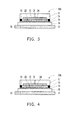
- FIG. 3 is a schematic cross-sectional diagram along a cut line III-III shown in FIG. 1A .
- FIG. 4 is a schematic cross-sectional diagram along a cut line IV-IV shown in FIG. 1A .
- FIG. 5 is a top view illustrating another CBD apparatus according to an exemplary embodiment of the disclosure.
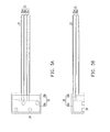
- FIG. 5A is a top view illustrating a solution input/output device shown in FIG. 5 .
- FIG. 5B is a cross-sectional diagram illustrating the solution input/output device shown in FIG. 5 .
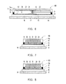
- FIG. 6 is a schematic cross-sectional diagram along a cut line VI-VI shown in FIG. 5 .
- FIG. 7 and FIG. 8 are schematic cross-sectional diagrams along a cut line VII-VII shown in FIG. 5 .
- FIG. 9 is a cross-sectional diagram illustrating another CBD apparatus according to an exemplary embodiment of the disclosure.
- FIG. 9A is a top view illustrating a solution input/output device shown in FIG. 9 .
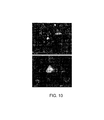
- FIG. 10 is an electron microscope photograph of a deposited and uncleaned film.
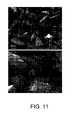
- FIG. 11 is an electron microscope photograph of a film that is cleaned after being deposited by using a CBD apparatus according to an exemplary embodiment of the disclosure.
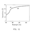
- FIG. 12 illustrates transmittance of a deposited and uncleaned film and a film that is cleaned after being deposited by using an apparatus according to an exemplary embodiment of the disclosure.
- FIG. 13A is a top view illustrating a CBD apparatus moving in a rotation mode according to an exemplary embodiment of the disclosure.
- FIG. 13B is a top view illustrating a CBD apparatus moving in a revolution mode according to an exemplary embodiment of the disclosure.
- FIG. 14A is an image of a film by vertically shaking the plating solution.
- FIG. 14B is an image of a film formed by horizontally shaking the plating solution moving in revolution mode.
- FIG.15 is a comparison figure in which transmittances are measured at different positions respectively for the film formed by vertical shaking and revolutionary shaking.
- a CBD apparatus 10A includes a first cap 11, a second cap 15, and a solution input/output device 12.
- the second cap 15 is arranged corresponding to the first cap 11, to form a deposition space 20.
- the first cap 11 can avoid the change in composition of a plating solution caused by escape of a volatile material in the plating solution, so as to maintain the quality of a deposited film.
- a material of the first cap 11 may include a high heat-preservation material, a corrosion resistant material, and those having low surface energy or all of the above properties.
- the first cap 11 may be a substrate made of an inorganic material, a conductive material, a polymer, or a composite material.
- the inorganic material is, for example, glass, quartz, ceramic, or alumina.
- the conductive material includes a metal or an alloy, for example, aluminum alloy, titanium, or molybdenum.
- the polymer is, for example, polyvinyl chloride (PVC), polytetrafluoroethylene (PTFE), or polypropylene (PP).
- PVC polyvinyl chloride
- PTFE polytetrafluoroethylene
- PP polypropylene
- first cap 11 may further provide a downward pressure on the second cap 15, by which the influence caused by a plating solution effluent in the deposition process to the quality of a deposited film can be effectively avoided.
- a weight of the first cap 11 is, for example, but not limited to, about 2 kg or higher.
- the first cap 11 may further provide a temperature control device 50 for heating and cooling the plating solution.
- the temperature control device 50 includes channels and heating rods or fluid in the channels.
- the plating solution may be heated by through the heating rods or heating the fluid in the channels.
- the plating solution may be cooled by cooling the fluid in the channels.
- the second cap 15 is a substrate to be deposited, and has a function of loading the plating solution.
- the second cap 15 may be substrate made of an inorganic material, a conductive material, semiconductive material, a polymer, or a composite material.
- the inorganic material is, for example, glass, quartz, or ceramic.
- the conductive material includes a metal, for example, an aluminum alloy, titanium, molybdenum, or stainless steel.
- the semiconductive material is, for example, silicon, CIGS, cadmium telluride, or other semiconductive materials having photoelectric conversion function.
- the polymer is, for example, polyimide (PI) or PTFE.
- another substrate 22 to be deposited may be further arranged on the first cap 11.
- the CBD apparatus 10A of the disclosure further has a spacer 14, which has a sealing function.
- the spacer 14 is located at an edge of the first cap 11 and the second cap 15, and the edge of either or both of the first cap 11 and the second cap 15 are engraved with a groove 19, so that the spacer 14 can be inserted in the first cap 11 or the second cap 15.
- the spacer 14 can provide a distance between the first cap 11 and the second cap 15, so as to form a space for accommodating the plating solution required by CBD.
- the distance provided between the first cap 11 and the second cap 15 by the spacer 14 is, for example, 5 mm to 70 mm; however, the disclosure is not limited thereto, and the distance can be adjusted according to an actual thickness of the substrate to be deposited.
- the spacer 14 can provide a distance between the first cap 11 and the second cap 15.
- the spacer 14 is required to have the properties of elasticity, acid and alkaline resistance, and low surface energy.
- the spacer 14 is, for example, an O-ring.
- a material of the O-ring is, for example, rubber, silicone, or PTFE.
- the size of the O-ring is that a perimeter is, for example, 100 mm, and a thickness is, for example, 2 mm.
- the groove 19 may be of a round shape, a square shape, or any other shape, and the shape of the groove 19 can be controlled to form a correspondingly different appearance of a deposited film.
- a height h1 of the deposition space 20 required for accommodating the plating solution by CBD is provided by the spacer 14; however, the disclosure is not limited thereto, and the height of the deposition space 20 may also be provided by changing the design of the first cap 11 or the second cap 15.
- the first cap 11 of a CBD apparatus 10B and 10C includes a body portion 11a and an extension portion 11b.
- the extension portion 11b of the first cap 11 extends downward from the body portion 11a, and provides, together with the spacer 14, a height h2 of the deposition space 20.
- a height h3 of the deposition space 20 is provided by the extension portion 11b of the first cap 11.
- the height h1, h2, or h3 of the deposition space 20 is, for example, 5 mm to 70 mm; however, the disclosure is not limited thereto, and the height can be adjusted according to practical requirement.
- the solution input/output device 12 is disposed in the first cap 11.
- the position of the solution input/output device 12 may be fixed (as shown in FIG. 1A to FIG. 4 ), or the solution input/output device 12 is movable in the deposition space 20 (as shown in FIG. 5 to FIG. 8 ).
- the solution input/output device 12 includes an arm 23 able to perform stretching motion and a solution injection chamber 26.
- the solution input/output device 12 is disposed on the extension portion 11b of the first cap 11 by the arm 23.
- the arm 23 has a solution pipe 25 therein, which can supply a fluid to the solution input/output device 12, and by the stretching of the movable arm 23, the solution input/output device 12 can move in the deposition space 20.
- the solution input/output device 12 is disposed on the extension portion 11b of the first cap 11, if an adequate distance exists between the body portion 11a of the first cap 11 and the solution input/output device 12, another substrate 22 to be deposited may be disposed on the body portion 11a of the first cap 11, so that the substrate to be deposited, that is, the second cap 15, and the another substrate to be deposited on the body portion 11a of the first cap 11 are deposited simultaneously by full filling the deposition space 20 with the plating solution.
- the solution input/output device 12 can provide a wetting solution, a plating solution, or a cleaning solution to the deposition space 20.
- the wetting solution is passed through the solution input/output device 12 to wet a surface of the substrate before the plating solution is introduced, so as to achieve the purpose of avoiding a decreased deposition coverage caused by the generation of micro-bubbles in subsequent injection of the plating solution, and the wetting action may be wetting the surface of the substrate first with a mist spayed by a mist nozzle.
- the cleaning solution can be used to remove impurities, for example, a KCN solution is used to remove CuSe series of compounds in a CIGS absorption layer, or solutions such as bromine in water may also be used to etch the substrate or remove a defect.
- the solution input/output device 12 may further have an ultrasonic vibration cleaning effect.
- the solution input/output device 12 further provide a route for solution input/output, pressure balancing, and gas input/output. Moreover, after the surface of the substrate is cleaned, air, argon, or nitrogen may be introduced in the deposition space by the solution input/output device 12, to remove moisture on the surface of the substrate to be deposited.
- a material of the solution input/output device 12 includes teflon, a metal, or a combination thereof, for example, aluminum, or stainless steel coated with teflon.
- FIG. 5A is a top view illustrating a solution input/output device according to an exemplary embodiment of the disclosure.
- FIG. 5B is a cross-sectional diagram illustrating the solution input/output device shown in FIG. 5A .
- FIG. 9A is a top view illustrating a solution input/output device shown in FIG. 9 .
- the solution pipe 25 disposed in the arm 23 of the solution input/output device 12 may be a single pipe or multiple pipes. If the solution pipe 25 is a single pipe, deionized water, a chemical reaction solution, or a gas may be supplied at different periods of time, that is, different solutions or gases flow in the same pipe. If the solution pipe 25 is multiple pipes, in an embodiment, as shown in FIG. 5A and FIG. 5B , the solution pipe 25 includes, for example, a pipe 25a, a pipe 25b, and a pipe 25c.
- the pipe 25a, the pipe 25b, and the pipe 25c may be respectively used to supply DI water, a chemical reaction solution, and a gas, so that different solutions or gases flow in different pipes.
- the liquids or gases supplied by the solution pipe 25 are not limited thereto.
- a pipe may be further added in the arm 23, which is connected to a pump, for discharging a waste liquid.
- the solution injection chamber 26 may have a single compartment, or is divided into two or more compartments according to practical requirement.
- the solution injection chamber 26 may be divided into a first compartment 26a and a second compartment 26b, in which the first compartment 26a may accommodate the chemical solution supplied by the pipe 25b, so as to provide a route through which the chemical solution enters the deposition space 20.
- the second compartment 26b may accommodate or hold DI water supplied by the pipe 25a and the gas supplied by the pipe 25c, and has an inlet/outlet 24 through which DI water and the gas enter the deposition space 20.
- the outlet/inlet 24 may be an inserted nozzle.
- Each compartment of the solution injection chamber 26 may have a single outlet/inlet 24 (as shown at a center of FIG. 1A ) or multiple outlets/inlets 24 (as shown at two sides of FIG. 1A ).
- the problem of pressure drop needs to be considered when a largely sized substrate is cleaned.
- the problem of pressure imbalance can be alleviated in case that multiple outlets/inlets 24 exist.
- the outlet/inlet 24 may be disposed at any position in the solution input/output device 12. In FIG. 3 , the outlet/inlet 24 is located at a bottom of the solution input/output device 12; however, the disclosure is not limited thereto.
- the solution input/output device 12 may spray the solution at any angle.
- the solution input/output device 12 can make the sprayed solution in a form of a mist, a film, or a pillar.
- the solution input/output device 12 may make the sprayed solution in a form of a vertical flow (as shown in FIG. 3 or 7 ) or an inclined flow (as shown in FIG. 4 or 8 ).
- the vertical flow is to vertically provide (jet) a solution to the substrate.
- the inclined flow can provide the solution to the whole deposition space 20, so as to expand a workable range of the apparatus.
- the inclined flow includes different spray forms, for example, a cross flow and an annular flow.
- the cross flow can avoid the disadvantage of poor removal of homogenous nucleation caused when two flows from different directions are simultaneously sprayed on the substrate.
- the pipe 25a is used to supply deionized water
- the air pipe 25c is used to supply air
- the pipe 25a and the pipe 25c may be connected to an external pump, so as to adjust the pressure of deionized water and gas supplied via the outlet/inlet 24, thereby achieving a cleaning purpose.
- the solution input/output device 12 may be connected to the extension portion 11b of the first cap 11 by a single arm 23 or multiple arms 23.
- multiple arms 23 exist; however, the disclosure is not limited thereto.
- a single pipe or multiple pipes may be disposed in each arm 23.
- each arm 23 has a pipe 25a, a pipe 25b, and a pipe 25c; however, the disclosure is not limited thereto.
- the solution injection chamber 26 may be divided into multiple regions according to practical requirement.
- the solution injection chamber 26 may be divided into a first region 27a, a second region 27b, and a third region 27c.
- the first region 27a, the second region 27b, and the third region 27c respectively have a first compartment 26a and a second compartment 26b. Details may be made reference to the description above and are not further described herein again. Through the disposition of multiple pipes, the problem of pressure drop caused by a too long pipe can be solved.
- the feeding inlet 21 may be of a round shape, a square shape, a rectangle shape, or any other shape.
- a diameter of a round feeding inlet is, for example, about 3-5 mm.
- the size of the feeding inlet 21 is suitably not excessively large, so as to avoid the influence caused by the evaporation of the plating solution to the quality of a deposited film.
- the feeding inlet 21 is opened to balance to pressure, which can facilitate the injection of the solution.
- the feeding inlet 21 may be located at any position in the solution input/output device.
- the CBD apparatus 10A, 10B, or 10C may further include a mixing device 16, which is disposed below the second cap 15.
- the mixing device 16 may include a heating unit and a shaking unit, for providing a heat source and mixing the solution.
- the heating unit can provide the heat source required in deposition, which may be a common heater, for example, resistance heating or infrared heating is employed.
- the heating unit may also be a material able to provide a heat source, for example, a material such as stainless steel or a copper block having a high thermal conductivity is immersed in a hot liquid, and then removed and used as a heat source after the temperature is stable.
- the heating unit in the mixing device 16 can be adjusted in a deposition process, so as to control a deposition rate.
- the deposition rate is generally proportional to the temperature; however, an excessively high temperature can result in massive homogeneous nucleation, which deteriorates the quality of a deposited film, and thus the deposition temperature is generally controlled to be in the range of 40-90°C, for example, about 70°C.
- FIG. 13A is a top view illustrating that a CBD apparatus moves in a rotation mode according to an exemplary embodiment of the disclosure.
- FIG. 13B is a top view illustrating that a CBD apparatus moves in a revolution mode according to an exemplary embodiment of the disclosure.
- the shaking unit in the mixing device 16 is connected to the second cap 15 so as to move the CBD apparatus 10A, 10B or 10C horizontally in a rotation mode or a revolution mode to shake the plating solution in the CBD apparatus 10A, 10B or 10C.
- the shaking unit in the mixing device 16 can be configured to make the CBD apparatus 10A, 10B or 10C rotate around a rotational axis passing through the center C of the CBD apparatus 10A, 10B or 10C.
- the shaking unit in the mixing device 16 also can be configured to make the CBD apparatus 10A, 10B or 10C move around a rotational axis beside the CBD apparatus 10A, 10B or 10C, so that a revolution around the rotational axis "O" can be carried out.
- the temperature can be controlled by the heating unit in the mixing device 16 in the CBD apparatus 10A, 10B, or 10C
- the material of the second cap 15 is conductive material such as stainless steel or titanium plate
- a voltage can be directly applied to the second cap 15 by using the conductive property thereof, and then the level of the applied voltage is controlled, to achieve the purpose of controlling the temperature of the solution in the deposition space 20.
- the mixing device 16 is made of a magnetic material
- a magnet may be positioned in the first cap 11.
- a magnetic force of the first cap 11 attracts the lower mixing device 16, so as to provide a pressure, thereby enhancing the tightness between the first cap 11 and the second cap 15, and avoiding the problem of leakage of the solution.
- the CBD apparatus 10A, 10B, or 10C may further include a tilt device17, or further include a tilt stand 18.
- the tilt stand 18 can tilts the tilt device 17, and maintains the tilt device at a specific angle.
- the tilt device 17 is disposed below the second cap 15, for tilting the CBD apparatus 10A, 10B, or 10C, so as to pool the solution in the deposition space 20, and especially discharge the remaining plating solution, cleaning solution, or wetting solution via the feeding inlet 21 in the first cap 11 after a deposited film is formed.
- the feeding inlet 21 may further serve as a drainage hole of the waste liquid.
- the waste liquid and waste gas generated in the above process can be discharged through the outlet/inlet 24 of the solution input/output device 12 via the feeding inlet 21.
- the first cap 11 may further include an opening 13 (as shown in FIG. 9 ), which is located at a position close to the edge of the first cap 11.
- the opening 13 may be extended into the deposition space 20 through a pipe fitting, and used as a discharge route of the waste liquid.
- the solution input/output device 12 may move to a position close to the edge of the first cap 11, and the waste liquid and waste gas pooled at the edge due to tilt can be discharged through the outlet/inlet 24 of the solution input/output device 12 via the feeding inlet 21.
- the waste liquid discharged via the feeding inlet 21 or the opening 13 may be collected in a waste liquid barrel for recycle.
- CBD apparatus of the disclosure A method of using the CBD apparatus of the disclosure is described below with reference to an example in which a CdS film is deposited.
- Deposition is carried out with a substrate to be deposited and having an area of about 100 cm 2 , and 20 ml of a plating solution containing 0.0015 M cadmium sulfate, 1 M aqueous ammonia, and 0.0075 M thiourea, in which an average height of the solution is about 2 mm, and a deposition temperature is controlled to be 70°C.
- the substrate to be deposited is positioned above the mixing device 16 first, and served as the second cap 15, on which the plating solution is loaded.
- glass is used as the second cap 15.
- the mixing device 16 uses a material (e.g. copper) having a high thermal conductivity as a heat source.
- the first cap 11 and the spacer 14 are positioned on the second cap 15, and the spacer 14 is inserted in the first cap 11 by means of the groove 19 at the edge of the first cap 11.
- the material of the first cap 11 is PTFE, which is acid and alkaline resistant and can be easily cleaned after deposition.
- An O-ring of perfluorinated rubber material is used as the spacer 14, and the size of the O-ring is that a perimeter is about 100 mm, and a thickness is about 2 mm. It is found through experiment that no degradation problem occurs even when the O-ring experiences 300 times of deposition.
- the first cap 11 further provide a downward pressure on the second cap 15, by which the influence caused by a plating solution effluent in the deposition process to the quality of a deposited film can be effectively avoided.
- the weight of the first cap 11 in the experiment is about 2 kg, and in the presence of the downward pressure provided by the first cap 11, there is no concern about leakage of the plating solution in the deposition experiment.
- the deposition space 20 may be first cleaned or wetted by the solution input/output device 12.
- the mixing device 16 is adjusted to control the deposition speed.
- the deposition temperature is, for example, controlled to be in the range of 40-90°C, and the deposition temperature in the experiment is 70°C.
- deposition parameters may be controlled to obtain a specific film thickness.
- the plating solution can be discharged by the solution input/output device 12 through the feeding inlet 21, or discharged via the opening 13.
- a degree of tilt of the deposition apparatus can be controlled by the tilt stand 18 in the tilt device 17, to facilitate the discharge of the solution.
- the cleaning process has a significant effect on the quality of a deposited film, which can remove homogenously nucleated particles attached to a surface in the deposition process.
- the solution input/output device 12 may clean the surface when being fixedly disposed as shown in FIG. 1A and FIG. 2A , or clean the surface when being movable disposed as shown in FIG. 5 and FIG. 6 .
- a cleaning manner may be rinsing an outer surface of the substrate with a water, or cleaning the surface by ultrasonic vibration.
- the solution input/output device 12 shown in FIG. 1A to FIG. 9 further provide a route for solution input/output, pressure balancing, and gas input/output.
- air, argon, or nitrogen may be introduced in the deposition space 20 by the solution input/output device 12, to remove moisture on the surface of the substrate to be deposited.
- a waste liquid, and waste gas generated in the above process are discharged by the solution input/output device 12 and collected in a waste liquid barrel for recovery.
- the process time is 20 min, and a thickness of a film thus fabricated is about 80 nm.
- FIG. 10 is an electron microscope photograph of a deposited and uncleaned film.
- FIG. 11 is an electron microscope photograph of a film that is cleaned after being deposited by using a CBD apparatus according to an exemplary embodiment of the disclosure. It can be clearly seen from the photographs that after cleaning by using the CBD apparatus of the disclosure, impurities on the surface of the deposited film can be effectively removed.
- FIG. 12 illustrates transmittance of a deposited and uncleaned film and a film that is cleaned after being deposited by using a CBD apparatus according to an exemplary embodiment of the disclosure.
- the results obtained from FIG. 12 shows that the transmittance represented by a curve 100 of the cleaned deposited film is obviously improved compared with that represented by a curve 200 of the uncleaned deposited film.
- Table 1 shows electrical performances of a film that is deposited through CBD and uncleaned.
- Table 2 shows electrical performances of a film that is cleaned after being deposited by using the CBD apparatus of the disclosure. The results of Table 1 and Table 2 show that the electrical performances of the cleaned deposited film are superior to those of the uncleaned deposited film.
- FIG. 14A is an image of a film formed by vertically shaking the CBD apparatus having the plating solution therein.
- FIG. 14B is an image of a film formed by horizontally shaking the CBD apparatus having the plating solution therein in revolution mode.
- FIG.15 is a comparison figure in which transmittances are measured at different positions respectively for the film formed by vertically shaking and horizontally shaking (revolution mode). In FIG. 15 , the measuring position is marked at the right down corner.
- the film at the peripheral edge of the glass substrate is not uniform.
- the plating solution can cover the surface of the glass substrate sufficiently, and no portion is exposed to contact with air. Therefore, the uniformity of the film on the peripheral edge of the glass substrate is very well.
- the variation of the transmittance for the film formed by vertically shaking reaches up to 2%, while variation of the transmittance for the film formed by horizontally shaking (revolution mode) is only 0.5%. Therefore, it is obvious that the film formed by horizontally shaking (revolution mode) can provide a better film uniformity.
- the chemical bath process can be effectively improved and simplified through the special cap design. Because the deposition apparatus of the disclosure is simple, and a crucible is not needed to be used, the cost of crucible is saved, and the volume of waste liquid generated is reduced. Furthermore, in the disclosure, the quality of a chip after deposition can be greatly improved through the special chip cleaning design, so that the disclosure can be widely used in chemical bath deposition of a semiconductor compound film, for example, the fabrication of a buffer layer of a solar cell.
Landscapes
- Chemical & Material Sciences (AREA)
- Inorganic Chemistry (AREA)
- Physics & Mathematics (AREA)
- Thermal Sciences (AREA)
- General Chemical & Material Sciences (AREA)
- Chemical Kinetics & Catalysis (AREA)
- Engineering & Computer Science (AREA)
- Materials Engineering (AREA)
- Mechanical Engineering (AREA)
- Metallurgy (AREA)
- Organic Chemistry (AREA)
- Chemically Coating (AREA)
- Sampling And Sample Adjustment (AREA)
- Electroplating Methods And Accessories (AREA)
Abstract
Description
- This application claims the priority benefit of Taiwan application serial no.
100146215, filed on December 14, 2011 - The disclosure relates to a liquid phase deposition apparatus, and particularly to a chemical bath deposition (CBD) apparatus.
- CBD is a liquid phase deposition process widely used in many industries at present. The most common CBD is conducted in a chemical tank. However, the volume of the chemical tank is quite large, and thus large amount of chemical plating solution must be used, leading to a decreased solution utilization, which not only causes a high deposition cost, but also incurs a major problem of wastewater treatment. Another CBD is to locate a substrate to be deposited in a crucible with a surface facing upward, and then pour a solution into the crucible to cover the substrate to be deposited, so as to perform the deposition. However, in the deposition process, the plating solution is also deposited on the crucible, which not only lowers the plating solution utilization, but also increases the process time because the crucible is required to be cleaned after deposition. For example, for the fabrication cost of a Cu(InGa)Se2 (CIGS) solar cell, a buffer layer plays a very important role. In case that a CdS buffer layer with a thickness of 50 nm is fabricated through a traditional CBD, the cost thereof accounts for 20% (excluding a substrate) of the cost of the cell, and thus the fabrication cost of the cell can be greatly lowered if the disadvantage can be effectively alleviated. In addition, in the traditional CBD, accompanying the cluster-cluster growth mechanism, ions in the solution form solid particles in the solution first, and then are adhered to the solid substrate, so that the formed film is opaque, uneven, and poor in adhesion. Therefore, if nucleated particles on the substrate can be removed effectively, the cell efficiency can be effectively improved.
- A CBD apparatus is introduced herein, by which the process can be simplified, the energy can be saved, the volume of wastewater can be reduced, the film quality can be improved, and the apparatus cost can be lowered.
- The disclosure provides a CBD apparatus, which includes a first cap, a second cap, and a solution input/output device. The second cap is arranged corresponding to the first cap so as to form a deposition space. The solution input/output device is disposed in the first cap, so as to feed a solution into/out of the deposition space. The position of the solution input/output device is fixed, or the solution input/output device is movable in the deposition space.
- Several exemplary embodiments accompanied with figures are described in detail below to further describe the disclosure in details.
- The accompanying drawings are included to provide further understanding, and are incorporated in and constitute a part of this specification. The drawings illustrate exemplary embodiments and, together with the description, serve to explain the principles of the disclosure.
-
FIG. 1A is a top view illustrating a CBD apparatus according to an exemplary embodiment of the disclosure. -
FIG. 1B is a top view illustrating a CBD apparatus according to another exemplary embodiment of the disclosure. -
FIG. 2A is a schematic cross-sectional diagram along a cut line II-II shown inFIG. 1A . -
FIG. 2B is a schematic cross-sectional diagram along a cut line II'-II' shown inFIG. 1B . -
FIG. 3 is a schematic cross-sectional diagram along a cut line III-III shown inFIG. 1A . -
FIG. 4 is a schematic cross-sectional diagram along a cut line IV-IV shown inFIG. 1A . -
FIG. 5 is a top view illustrating another CBD apparatus according to an exemplary embodiment of the disclosure. -
FIG. 5A is a top view illustrating a solution input/output device shown inFIG. 5 . -
FIG. 5B is a cross-sectional diagram illustrating the solution input/output device shown inFIG. 5 . -
FIG. 6 is a schematic cross-sectional diagram along a cut line VI-VI shown inFIG. 5 . -
FIG. 7 and FIG. 8 are schematic cross-sectional diagrams along a cut line VII-VII shown inFIG. 5 . -
FIG. 9 is a cross-sectional diagram illustrating another CBD apparatus according to an exemplary embodiment of the disclosure. -
FIG. 9A is a top view illustrating a solution input/output device shown inFIG. 9 . -
FIG. 10 is an electron microscope photograph of a deposited and uncleaned film. -
FIG. 11 is an electron microscope photograph of a film that is cleaned after being deposited by using a CBD apparatus according to an exemplary embodiment of the disclosure. -
FIG. 12 illustrates transmittance of a deposited and uncleaned film and a film that is cleaned after being deposited by using an apparatus according to an exemplary embodiment of the disclosure. -
FIG. 13A is a top view illustrating a CBD apparatus moving in a rotation mode according to an exemplary embodiment of the disclosure. -
FIG. 13B is a top view illustrating a CBD apparatus moving in a revolution mode according to an exemplary embodiment of the disclosure. -
FIG. 14A is an image of a film by vertically shaking the plating solution. -
FIG. 14B is an image of a film formed by horizontally shaking the plating solution moving in revolution mode. -
FIG.15 is a comparison figure in which transmittances are measured at different positions respectively for the film formed by vertical shaking and revolutionary shaking. - For simplicity, in the embodiments below, the same elements are represented by the same numerals. In addition, sizes or shapes of the elements in the drawings are exemplary, and are not entirely scaled according to actual sizes or shapes of the elements.
- Referring to
FIG. 1A and FIG. 2A , aCBD apparatus 10A includes afirst cap 11, asecond cap 15, and a solution input/output device 12. - The
second cap 15 is arranged corresponding to thefirst cap 11, to form adeposition space 20. Thefirst cap 11 can avoid the change in composition of a plating solution caused by escape of a volatile material in the plating solution, so as to maintain the quality of a deposited film. In an embodiment, a material of thefirst cap 11 may include a high heat-preservation material, a corrosion resistant material, and those having low surface energy or all of the above properties. Thefirst cap 11 may be a substrate made of an inorganic material, a conductive material, a polymer, or a composite material. The inorganic material is, for example, glass, quartz, ceramic, or alumina. The conductive material includes a metal or an alloy, for example, aluminum alloy, titanium, or molybdenum. The polymer is, for example, polyvinyl chloride (PVC), polytetrafluoroethylene (PTFE), or polypropylene (PP). It should be noted that PTFE is acid and alkaline resistant, and has a low surface energy, and particles in the solution are difficult to nucleate thereon, so that thefirst cap 11 is made of PTFE, and a surface thereof can be easily cleaned after a deposited film is formed. - In addition, the
first cap 11 may further provide a downward pressure on thesecond cap 15, by which the influence caused by a plating solution effluent in the deposition process to the quality of a deposited film can be effectively avoided. A weight of thefirst cap 11 is, for example, but not limited to, about 2 kg or higher. - Referring to
Fig. 1B and Fig. 2B , thefirst cap 11 may further provide atemperature control device 50 for heating and cooling the plating solution. Thetemperature control device 50 includes channels and heating rods or fluid in the channels. The plating solution may be heated by through the heating rods or heating the fluid in the channels. The plating solution may be cooled by cooling the fluid in the channels. - The
second cap 15 is a substrate to be deposited, and has a function of loading the plating solution. Thesecond cap 15 may be substrate made of an inorganic material, a conductive material, semiconductive material, a polymer, or a composite material. The inorganic material is, for example, glass, quartz, or ceramic. The conductive material includes a metal, for example, an aluminum alloy, titanium, molybdenum, or stainless steel. The semiconductive material is, for example, silicon, CIGS, cadmium telluride, or other semiconductive materials having photoelectric conversion function. The polymer is, for example, polyimide (PI) or PTFE. In another embodiment, referring toFIG. 6 , anothersubstrate 22 to be deposited may be further arranged on thefirst cap 11. - Further referring to
FIG. 1A and FIG. 2A , in an embodiment, theCBD apparatus 10A of the disclosure further has aspacer 14, which has a sealing function. Thespacer 14 is located at an edge of thefirst cap 11 and thesecond cap 15, and the edge of either or both of thefirst cap 11 and thesecond cap 15 are engraved with agroove 19, so that thespacer 14 can be inserted in thefirst cap 11 or thesecond cap 15. In the embodiments shown inFIG. 1A to FIG. 4 , thespacer 14 can provide a distance between thefirst cap 11 and thesecond cap 15, so as to form a space for accommodating the plating solution required by CBD. The distance provided between thefirst cap 11 and thesecond cap 15 by thespacer 14 is, for example, 5 mm to 70 mm; however, the disclosure is not limited thereto, and the distance can be adjusted according to an actual thickness of the substrate to be deposited. In an embodiment, thespacer 14 can provide a distance between thefirst cap 11 and thesecond cap 15. Thespacer 14 is required to have the properties of elasticity, acid and alkaline resistance, and low surface energy. Thespacer 14 is, for example, an O-ring. A material of the O-ring is, for example, rubber, silicone, or PTFE. The size of the O-ring is that a perimeter is, for example, 100 mm, and a thickness is, for example, 2 mm. Thegroove 19 may be of a round shape, a square shape, or any other shape, and the shape of thegroove 19 can be controlled to form a correspondingly different appearance of a deposited film. - In the embodiments shown in
FIG. 1A to FIG. 4 , a height h1 of thedeposition space 20 required for accommodating the plating solution by CBD is provided by thespacer 14; however, the disclosure is not limited thereto, and the height of thedeposition space 20 may also be provided by changing the design of thefirst cap 11 or thesecond cap 15. For example, referring toFIG. 6 to FIG. 8 andFIG. 9 , thefirst cap 11 of aCBD apparatus body portion 11a and anextension portion 11b. InFIG. 6 to FIG. 8 , theextension portion 11b of thefirst cap 11 extends downward from thebody portion 11a, and provides, together with thespacer 14, a height h2 of thedeposition space 20. InFIG. 9 , a height h3 of thedeposition space 20 is provided by theextension portion 11b of thefirst cap 11. - The height h1, h2, or h3 of the
deposition space 20 is, for example, 5 mm to 70 mm; however, the disclosure is not limited thereto, and the height can be adjusted according to practical requirement. - Referring to
FIG. 1A to FIG. 8 , the solution input/output device 12 is disposed in thefirst cap 11. The position of the solution input/output device 12 may be fixed (as shown inFIG. 1A to FIG. 4 ), or the solution input/output device 12 is movable in the deposition space 20 (as shown inFIG. 5 to FIG. 8 ). - Referring to
FIGs. 5 to 6 , the solution input/output device 12 includes anarm 23 able to perform stretching motion and asolution injection chamber 26. The solution input/output device 12 is disposed on theextension portion 11b of thefirst cap 11 by thearm 23. Thearm 23 has asolution pipe 25 therein, which can supply a fluid to the solution input/output device 12, and by the stretching of themovable arm 23, the solution input/output device 12 can move in thedeposition space 20. - Moreover, as the solution input/
output device 12 is disposed on theextension portion 11b of thefirst cap 11, if an adequate distance exists between thebody portion 11a of thefirst cap 11 and the solution input/output device 12, anothersubstrate 22 to be deposited may be disposed on thebody portion 11a of thefirst cap 11, so that the substrate to be deposited, that is, thesecond cap 15, and the another substrate to be deposited on thebody portion 11a of thefirst cap 11 are deposited simultaneously by full filling thedeposition space 20 with the plating solution. - The solution input/
output device 12 can provide a wetting solution, a plating solution, or a cleaning solution to thedeposition space 20. The wetting solution is passed through the solution input/output device 12 to wet a surface of the substrate before the plating solution is introduced, so as to achieve the purpose of avoiding a decreased deposition coverage caused by the generation of micro-bubbles in subsequent injection of the plating solution, and the wetting action may be wetting the surface of the substrate first with a mist spayed by a mist nozzle. The cleaning solution can be used to remove impurities, for example, a KCN solution is used to remove CuSe series of compounds in a CIGS absorption layer, or solutions such as bromine in water may also be used to etch the substrate or remove a defect. In addition, the solution input/output device 12 may further have an ultrasonic vibration cleaning effect. - In addition to the substrate cleaning effect, the solution input/
output device 12 further provide a route for solution input/output, pressure balancing, and gas input/output. Moreover, after the surface of the substrate is cleaned, air, argon, or nitrogen may be introduced in the deposition space by the solution input/output device 12, to remove moisture on the surface of the substrate to be deposited. - A material of the solution input/
output device 12 includes teflon, a metal, or a combination thereof, for example, aluminum, or stainless steel coated with teflon. -
FIG. 5A is a top view illustrating a solution input/output device according to an exemplary embodiment of the disclosure.FIG. 5B is a cross-sectional diagram illustrating the solution input/output device shown inFIG. 5A .FIG. 9A is a top view illustrating a solution input/output device shown inFIG. 9 . - Referring to
FIGs. 5 ,5A, and 5B , thesolution pipe 25 disposed in thearm 23 of the solution input/output device 12 may be a single pipe or multiple pipes. If thesolution pipe 25 is a single pipe, deionized water, a chemical reaction solution, or a gas may be supplied at different periods of time, that is, different solutions or gases flow in the same pipe. If thesolution pipe 25 is multiple pipes, in an embodiment, as shown inFIG. 5A and FIG. 5B , thesolution pipe 25 includes, for example, a pipe 25a, apipe 25b, and a pipe 25c. The pipe 25a, thepipe 25b, and the pipe 25c may be respectively used to supply DI water, a chemical reaction solution, and a gas, so that different solutions or gases flow in different pipes. However, the liquids or gases supplied by thesolution pipe 25 are not limited thereto. In addition to, a pipe may be further added in thearm 23, which is connected to a pump, for discharging a waste liquid. - Furthermore, referring to
FIGs. 5 ,5A, and 5B , thesolution injection chamber 26 may have a single compartment, or is divided into two or more compartments according to practical requirement. In an embodiment, thesolution injection chamber 26 may be divided into afirst compartment 26a and asecond compartment 26b, in which thefirst compartment 26a may accommodate the chemical solution supplied by thepipe 25b, so as to provide a route through which the chemical solution enters thedeposition space 20. Thesecond compartment 26b may accommodate or hold DI water supplied by the pipe 25a and the gas supplied by the pipe 25c, and has an inlet/outlet 24 through which DI water and the gas enter thedeposition space 20. The outlet/inlet 24 may be an inserted nozzle. Each compartment of thesolution injection chamber 26 may have a single outlet/inlet 24 (as shown at a center ofFIG. 1A ) or multiple outlets/inlets 24 (as shown at two sides ofFIG. 1A ). For the single outlet/inlet 24, the problem of pressure drop needs to be considered when a largely sized substrate is cleaned. The problem of pressure imbalance can be alleviated in case that multiple outlets/inlets 24 exist. The outlet/inlet 24 may be disposed at any position in the solution input/output device 12. InFIG. 3 , the outlet/inlet 24 is located at a bottom of the solution input/output device 12; however, the disclosure is not limited thereto. InFIG. 6 , the solution input/output device 12 may spray the solution at any angle. The solution input/output device 12 can make the sprayed solution in a form of a mist, a film, or a pillar. For example, the solution input/output device 12 may make the sprayed solution in a form of a vertical flow (as shown inFIG. 3 or7 ) or an inclined flow (as shown inFIG. 4 or8 ). The vertical flow is to vertically provide (jet) a solution to the substrate. The inclined flow can provide the solution to thewhole deposition space 20, so as to expand a workable range of the apparatus. The inclined flow includes different spray forms, for example, a cross flow and an annular flow. The cross flow can avoid the disadvantage of poor removal of homogenous nucleation caused when two flows from different directions are simultaneously sprayed on the substrate. - In an embodiment, the pipe 25a is used to supply deionized water, the air pipe 25c is used to supply air, and the pipe 25a and the pipe 25c may be connected to an external pump, so as to adjust the pressure of deionized water and gas supplied via the outlet/
inlet 24, thereby achieving a cleaning purpose. - In addition, referring to
FIG. 9 , and9A , if the solution input/output device 12 has a large size, the solution input/output device 12 may be connected to theextension portion 11b of thefirst cap 11 by asingle arm 23 ormultiple arms 23. In the solution input/output device 12 shown inFIG. 9A ,multiple arms 23 exist; however, the disclosure is not limited thereto. Likewise, a single pipe or multiple pipes may be disposed in eacharm 23. In the figure, eacharm 23 has a pipe 25a, apipe 25b, and a pipe 25c; however, the disclosure is not limited thereto. Thesolution injection chamber 26 may be divided into multiple regions according to practical requirement. In an embodiment, thesolution injection chamber 26 may be divided into a first region 27a, asecond region 27b, and athird region 27c. The first region 27a, thesecond region 27b, and thethird region 27c respectively have afirst compartment 26a and asecond compartment 26b. Details may be made reference to the description above and are not further described herein again. Through the disposition of multiple pipes, the problem of pressure drop caused by a too long pipe can be solved. - Referring to
FIG. 1A to FIG. 8 , materials are supplied into the solution input/output device 12 through a feedinginlet 21 in thefirst cap 11, and then the solution input/output device 12 provides the wetting solution, the plating solution, or the cleaning solution to thedeposition space 20. The feedinginlet 21 may be of a round shape, a square shape, a rectangle shape, or any other shape. A diameter of a round feeding inlet is, for example, about 3-5 mm. The size of the feedinginlet 21 is suitably not excessively large, so as to avoid the influence caused by the evaporation of the plating solution to the quality of a deposited film. During feeding, the feedinginlet 21 is opened to balance to pressure, which can facilitate the injection of the solution. The feedinginlet 21 may be located at any position in the solution input/output device. - The
CBD apparatus mixing device 16, which is disposed below thesecond cap 15. The mixingdevice 16 may include a heating unit and a shaking unit, for providing a heat source and mixing the solution. The heating unit can provide the heat source required in deposition, which may be a common heater, for example, resistance heating or infrared heating is employed. The heating unit may also be a material able to provide a heat source, for example, a material such as stainless steel or a copper block having a high thermal conductivity is immersed in a hot liquid, and then removed and used as a heat source after the temperature is stable. The heating unit in themixing device 16 can be adjusted in a deposition process, so as to control a deposition rate. The deposition rate is generally proportional to the temperature; however, an excessively high temperature can result in massive homogeneous nucleation, which deteriorates the quality of a deposited film, and thus the deposition temperature is generally controlled to be in the range of 40-90°C, for example, about 70°C. -
FIG. 13A is a top view illustrating that a CBD apparatus moves in a rotation mode according to an exemplary embodiment of the disclosure. -
FIG. 13B is a top view illustrating that a CBD apparatus moves in a revolution mode according to an exemplary embodiment of the disclosure. - Referring to
FIG. 13A andFIG. 13B , the shaking unit in themixing device 16 is connected to thesecond cap 15 so as to move theCBD apparatus CBD apparatus FIG. 13A , the shaking unit in themixing device 16 can be configured to make theCBD apparatus CBD apparatus FIG. 13B , the shaking unit in themixing device 16 also can be configured to make theCBD apparatus CBD apparatus - Furthermore, besides that the temperature can be controlled by the heating unit in the
mixing device 16 in theCBD apparatus second cap 15 is conductive material such as stainless steel or titanium plate, a voltage can be directly applied to thesecond cap 15 by using the conductive property thereof, and then the level of the applied voltage is controlled, to achieve the purpose of controlling the temperature of the solution in thedeposition space 20. - In addition, if the mixing
device 16 is made of a magnetic material, a magnet may be positioned in thefirst cap 11. When thefirst cap 11 is positioned above the mixingdevice 16, a magnetic force of thefirst cap 11 attracts thelower mixing device 16, so as to provide a pressure, thereby enhancing the tightness between thefirst cap 11 and thesecond cap 15, and avoiding the problem of leakage of the solution. - The
CBD apparatus tilt stand 18. The tilt stand 18 can tilts thetilt device 17, and maintains the tilt device at a specific angle. Thetilt device 17 is disposed below thesecond cap 15, for tilting theCBD apparatus deposition space 20, and especially discharge the remaining plating solution, cleaning solution, or wetting solution via the feedinginlet 21 in thefirst cap 11 after a deposited film is formed. - More particularly, referring to
FIG. 1A and FIG. 2A , if the solution input/output device 12 is fixedly disposed at a position close to the edge of thefirst cap 11, when the solution in thedeposition space 20 is pooled to the edge due to tilt, the feedinginlet 21 may further serve as a drainage hole of the waste liquid. The waste liquid and waste gas generated in the above process can be discharged through the outlet/inlet 24 of the solution input/output device 12 via the feedinginlet 21. If the solution input/output device 12 is fixedly disposed a position close to the center of thefirst cap 11, thefirst cap 11 may further include an opening 13 (as shown inFIG. 9 ), which is located at a position close to the edge of thefirst cap 11. When the solution in thedeposition space 20 is pooled at the edge due to tilt, theopening 13 may be extended into thedeposition space 20 through a pipe fitting, and used as a discharge route of the waste liquid. Referring toFIG. 5 andFIG. 6 , if the solution input/output device 12 is movably disposed in thefirst cap 11, the solution input/output device 12 may move to a position close to the edge of thefirst cap 11, and the waste liquid and waste gas pooled at the edge due to tilt can be discharged through the outlet/inlet 24 of the solution input/output device 12 via the feedinginlet 21. The waste liquid discharged via the feedinginlet 21 or theopening 13 may be collected in a waste liquid barrel for recycle. - A method of using the CBD apparatus of the disclosure is described below with reference to an example in which a CdS film is deposited.
- Deposition is carried out with a substrate to be deposited and having an area of about 100 cm2, and 20 ml of a plating solution containing 0.0015 M cadmium sulfate, 1 M aqueous ammonia, and 0.0075 M thiourea, in which an average height of the solution is about 2 mm, and a deposition temperature is controlled to be 70°C.
- Referring to
FIG. 2A , in deposition, the substrate to be deposited is positioned above the mixingdevice 16 first, and served as thesecond cap 15, on which the plating solution is loaded. In this experiment, glass is used as thesecond cap 15. The mixingdevice 16 uses a material (e.g. copper) having a high thermal conductivity as a heat source. - In the deposition process, after the
second cap 15 is positioned above the mixingdevice 16, thefirst cap 11 and thespacer 14 are positioned on thesecond cap 15, and thespacer 14 is inserted in thefirst cap 11 by means of thegroove 19 at the edge of thefirst cap 11. In this embodiment, the material of thefirst cap 11 is PTFE, which is acid and alkaline resistant and can be easily cleaned after deposition. An O-ring of perfluorinated rubber material is used as thespacer 14, and the size of the O-ring is that a perimeter is about 100 mm, and a thickness is about 2 mm. It is found through experiment that no degradation problem occurs even when the O-ring experiences 300 times of deposition. - Besides the above functions, the
first cap 11 further provide a downward pressure on thesecond cap 15, by which the influence caused by a plating solution effluent in the deposition process to the quality of a deposited film can be effectively avoided. The weight of thefirst cap 11 in the experiment is about 2 kg, and in the presence of the downward pressure provided by thefirst cap 11, there is no concern about leakage of the plating solution in the deposition experiment. - After the
first cap 11 and thespacer 14 are covered on thesecond cap 15, materials is fed through the feedinginlet 21, in which the diameter of the feedinginlet 21 is about 3-5mm. Before deposition, thedeposition space 20 may be first cleaned or wetted by the solution input/output device 12. In the deposition process, the mixingdevice 16 is adjusted to control the deposition speed. The deposition temperature is, for example, controlled to be in the range of 40-90°C, and the deposition temperature in the experiment is 70°C. - In the deposition process, deposition parameters may be controlled to obtain a specific film thickness. After deposition, the plating solution can be discharged by the solution input/
output device 12 through the feedinginlet 21, or discharged via theopening 13. In discharge of the solution, a degree of tilt of the deposition apparatus can be controlled by the tilt stand 18 in thetilt device 17, to facilitate the discharge of the solution. The cleaning process has a significant effect on the quality of a deposited film, which can remove homogenously nucleated particles attached to a surface in the deposition process. The solution input/output device 12 may clean the surface when being fixedly disposed as shown inFIG. 1A and FIG. 2A , or clean the surface when being movable disposed as shown inFIG. 5 andFIG. 6 . A cleaning manner may be rinsing an outer surface of the substrate with a water, or cleaning the surface by ultrasonic vibration. In addition to the substrate cleaning effect, the solution input/output device 12 shown inFIG. 1A to FIG. 9 further provide a route for solution input/output, pressure balancing, and gas input/output. After the surface of the substrate is cleaned, air, argon, or nitrogen may be introduced in thedeposition space 20 by the solution input/output device 12, to remove moisture on the surface of the substrate to be deposited. A waste liquid, and waste gas generated in the above process are discharged by the solution input/output device 12 and collected in a waste liquid barrel for recovery. The process time is 20 min, and a thickness of a film thus fabricated is about 80 nm. -
FIG. 10 is an electron microscope photograph of a deposited and uncleaned film.FIG. 11 is an electron microscope photograph of a film that is cleaned after being deposited by using a CBD apparatus according to an exemplary embodiment of the disclosure. It can be clearly seen from the photographs that after cleaning by using the CBD apparatus of the disclosure, impurities on the surface of the deposited film can be effectively removed. -
FIG. 12 illustrates transmittance of a deposited and uncleaned film and a film that is cleaned after being deposited by using a CBD apparatus according to an exemplary embodiment of the disclosure. The results obtained fromFIG. 12 shows that the transmittance represented by acurve 100 of the cleaned deposited film is obviously improved compared with that represented by acurve 200 of the uncleaned deposited film. -
Table 1 Cell Open-circuit voltage Voc (V) Short-circuit current density Jsc (mA/cm2) Fill factor F.F. (%) Efficiency Sheet resistance Rsh (Ohm) Resistance Rs (Ohm) Cell 1 0.00 0.000 Inf 0.009 NaN NaN Cell 2 0.59 25.106 47 6.933 1659 61 Cell 3 0.59 19.298 28 3.214 429 174 Cell 40.00 0.000 Inf 0.042 NaN NaN Cell 5 0.59 24.887 69 10.085 5674 24 Cell 60.00 0.000 Inf 0.024 NaN NaN -
Table 2 Cell Open-circ uit voltage Voc (V) Short-circuit current densityJsc (mA/cm2) Fill factor F.F. (%) Efficiency Sheet resistance Rsh (Ohm) Resistance Rs (Ohm) Cell 1 0.56 24.957 52 7.309 550 34 Cell 20.58 24.028 72 10.049 6378 23 Cell 3 0.58 25.262 72 10.487 3992 22 Cell 40.58 25.291 71 10.467 8748 22 Cell 50.57 23.922 65 8.892 1597 26 Cell 60.58 25.936 72 10.753 5447 22 - Table 1 shows electrical performances of a film that is deposited through CBD and uncleaned. Table 2 shows electrical performances of a film that is cleaned after being deposited by using the CBD apparatus of the disclosure. The results of Table 1 and Table 2 show that the electrical performances of the cleaned deposited film are superior to those of the uncleaned deposited film.
-
FIG. 14A is an image of a film formed by vertically shaking the CBD apparatus having the plating solution therein.FIG. 14B is an image of a film formed by horizontally shaking the CBD apparatus having the plating solution therein in revolution mode.FIG.15 is a comparison figure in which transmittances are measured at different positions respectively for the film formed by vertically shaking and horizontally shaking (revolution mode). InFIG. 15 , the measuring position is marked at the right down corner. - As shown in
FIG. 14A , when the film is formed by vertically shaking, the plating solution is not able to uniformly cover the surface of the glass substrate due to the plating solution shaking on the peripheral edge of the glass substrate. Therefore, the film at the peripheral edge of the glass substrate is not uniform. - In addition, as shown in
FIG. 14B , when the film is formed by horizontally shaking (revolution mode), the plating solution can cover the surface of the glass substrate sufficiently, and no portion is exposed to contact with air. Therefore, the uniformity of the film on the peripheral edge of the glass substrate is very well. According to the result shown inFIG. 15 , the variation of the transmittance for the film formed by vertically shaking reaches up to 2%, while variation of the transmittance for the film formed by horizontally shaking (revolution mode) is only 0.5%. Therefore, it is obvious that the film formed by horizontally shaking (revolution mode) can provide a better film uniformity. - To sum up, in the disclosure, the chemical bath process can be effectively improved and simplified through the special cap design. Because the deposition apparatus of the disclosure is simple, and a crucible is not needed to be used, the cost of crucible is saved, and the volume of waste liquid generated is reduced. Furthermore, in the disclosure, the quality of a chip after deposition can be greatly improved through the special chip cleaning design, so that the disclosure can be widely used in chemical bath deposition of a semiconductor compound film, for example, the fabrication of a buffer layer of a solar cell.
Claims (18)
- A chemical bath deposition (CBD) apparatus, comprising:a first cap (11) and a second cap (15), wherein the second cap (15) is arranged corresponding to the first cap (11) so as to form a deposition space (20); anda solution input/output device (12) located in the first cap (11), wherein the position of the solution input/output device (12) is fixed, or the solution input/output device (12) is movable in the deposition space (20).
- The CBD apparatus according to claim 1, further comprising a mixing device (17), arranged below the second cap (15).
- The CBD apparatus according to claim 2, wherein the mixing device (17) comprises a shaking unit.
- The CBD apparatus according to claim 3, wherein the shaking unit moves in a rotation mode or a revolution mode.
- The CBD apparatus according to claim 2, wherein the mixing device (17) comprises a heating unit.
- The CBD apparatus according to claim 1, wherein the first cap (11) comprises a temperature control device for heating and cooling.
- The CBD apparatus according to claim 1, further comprising a spacer (14) located at an edge of the first cap (11) or an edge of the second cap (15) has, so that the deposition space (20) is formed between the first cap (11) and the second cap (15).
- The CBD apparatus according to claim 5, wherein the edge of the second cap (15) or the first cap (11) has a groove (19), and the spacer (14) is arranged in the groove (19).
- The CBD apparatus according to claim 1, wherein the first cap (11) further comprises a magnetic substance therein.
- The CBD apparatus according to claim 1, wherein the second cap (15) is a substrate to be deposited.
- The CBD apparatus according to claim 1, wherein a substrate to be deposited is capable of being arranged on the first cap (11) in the deposition space (20).
- The CBD apparatus according to claim 1, further comprising a tilt device, arranged below the second cap (15).
- The CBD apparatus according to claim 1, wherein an outer edge of the first cap (11) has an extension portion (11b), for providing a height of the deposition space (20).
- The CBD apparatus according to claim 1, wherein the solution input/output device (12) comprises:at least one arm (23), connecting the extension portion (11b) of the first cap (11);at least one solution injection chamber (26), connecting the arm (23); andat least one solution pipe (25, 25a, 25b, 25c), located in the arm (23), for supplying a fluid to the solution injection chamber (26).
- The CBD apparatus according to claim 14, wherein the arm (23) is capable of performing stretching motion.
- The CBD apparatus according to claim 14, wherein the solution injection chamber (26) has at least one outlet/inlet (24).
- The CBD apparatus according to claim 16, wherein the outlet/inlet (24) comprises an embedded nozzle.
- The CBD apparatus according to claim 16, wherein the outlet/inlet (24) is located at any position in the solution input/output device (12).
Applications Claiming Priority (1)
| Application Number | Priority Date | Filing Date | Title |
|---|---|---|---|
| TW100146215A TWI458546B (en) | 2011-12-14 | 2011-12-14 | Chemical bath deposition (cbd) apparatus |
Publications (2)
| Publication Number | Publication Date |
|---|---|
| EP2604721A2 true EP2604721A2 (en) | 2013-06-19 |
| EP2604721A3 EP2604721A3 (en) | 2015-12-16 |
Family
ID=47115331
Family Applications (1)
| Application Number | Title | Priority Date | Filing Date |
|---|---|---|---|
| EP12188055.3A Withdrawn EP2604721A3 (en) | 2011-12-14 | 2012-10-10 | Chemical bath deposition (CBD) apparatus |
Country Status (4)
| Country | Link |
|---|---|
| US (1) | US9249507B2 (en) |
| EP (1) | EP2604721A3 (en) |
| CN (1) | CN103160815B (en) |
| TW (1) | TWI458546B (en) |
Families Citing this family (5)
| Publication number | Priority date | Publication date | Assignee | Title |
|---|---|---|---|---|
| TWI573287B (en) * | 2014-10-23 | 2017-03-01 | 亞智科技股份有限公司 | Chemical liquid recovery device and system and method thereof |
| CN111218675B (en) * | 2018-11-27 | 2023-10-03 | 上海祖强能源有限公司 | Chemical water bath deposition system and method of use |
| TWI689623B (en) * | 2019-07-16 | 2020-04-01 | 黃信航 | Chemical deposition equipment and method for continuous production piece by piece in horizontal inclined manner |
| WO2021119812A1 (en) * | 2019-12-17 | 2021-06-24 | Covalon Technologies Ltd. | Reactors for coating devices and related systems and methods |
| CN117051386B (en) * | 2023-07-10 | 2025-07-11 | 景德镇陶瓷大学 | Aluminum-doped zinc oxide transparent conductive film preparation equipment |
Family Cites Families (22)
| Publication number | Priority date | Publication date | Assignee | Title |
|---|---|---|---|---|
| US4335266A (en) | 1980-12-31 | 1982-06-15 | The Boeing Company | Methods for forming thin-film heterojunction solar cells from I-III-VI.sub.2 |
| WO2002099847A2 (en) * | 2001-06-04 | 2002-12-12 | Itn Energy Systems, Inc. | Apparatus and method for rotating drum chemical bath deposition |
| JP4330380B2 (en) * | 2003-05-29 | 2009-09-16 | 株式会社荏原製作所 | Plating apparatus and plating method |
| US6962626B1 (en) * | 2004-05-28 | 2005-11-08 | Xerox Corporation | Venting assembly for dip coating apparatus and related processes |
| TWI343840B (en) * | 2005-07-06 | 2011-06-21 | Applied Materials Inc | Apparatus for electroless deposition of metals onto semiconductor substrates |
| US7677198B2 (en) | 2005-11-28 | 2010-03-16 | Industrial Technology Research Institute | Method and apparatus for growing a composite metal sulphide photocatalyst thin film |
| US8354294B2 (en) | 2006-01-24 | 2013-01-15 | De Rochemont L Pierre | Liquid chemical deposition apparatus and process and products therefrom |
| US7541067B2 (en) | 2006-04-13 | 2009-06-02 | Solopower, Inc. | Method and apparatus for continuous processing of buffer layers for group IBIIIAVIA solar cells |
| US7923281B2 (en) | 2006-04-13 | 2011-04-12 | Solopower, Inc. | Roll-to-roll processing method and tools for electroless deposition of thin layers |
| JP4922889B2 (en) | 2006-11-06 | 2012-04-25 | パナソニック株式会社 | Optical space transmission system for performing optical space transmission and optical transmitter used therefor |
| US20080299411A1 (en) | 2007-05-30 | 2008-12-04 | Oladeji Isaiah O | Zinc oxide film and method for making |
| JP2011518942A (en) | 2007-10-17 | 2011-06-30 | ルション、ヤン | Improved solution deposition assembly |
| EP2257970A4 (en) | 2008-03-05 | 2015-09-02 | Hanergy Hi Tech Power Hk Ltd | BUFFER LAYER DEPOSITION FOR THIN FILM SOLAR BATTERIES |
| WO2009111055A1 (en) | 2008-03-05 | 2009-09-11 | Global Solar Energy, Inc. | Feedback for buffer layer deposition |
| TWM358403U (en) * | 2009-01-16 | 2009-06-01 | Dalux Technology Co Ltd | Device of flexible substrate for continuous chemical water-bathing deposition |
| CN201367462Y (en) * | 2009-02-04 | 2009-12-23 | 睿明科技股份有限公司 | Continuous chemical water bath deposition apparatus for flexible substrate |
| US8318530B2 (en) * | 2009-07-24 | 2012-11-27 | Solopower, Inc. | Solar cell buffer layer having varying composition |
| KR20110012550A (en) | 2009-07-30 | 2011-02-09 | 삼성전자주식회사 | Manufacturing method and apparatus for thin film solar cell |
| CN201567373U (en) * | 2009-11-20 | 2010-09-01 | 常州市正阳焊接材料有限公司 | Chemical plating device |
| DE102010006499A1 (en) | 2010-01-28 | 2011-08-18 | Würth Solar GmbH & Co. KG, 74523 | Bath separation solution for the wet-chemical deposition of a metal sulfide layer and associated production methods |
| TW201128791A (en) * | 2010-02-12 | 2011-08-16 | sheng-chang Zhang | Chemical water bath single-sided coating method and device thereof |
| US8726829B2 (en) | 2011-06-07 | 2014-05-20 | Jiaxiong Wang | Chemical bath deposition apparatus for fabrication of semiconductor films through roll-to-roll processes |
-
2011
- 2011-12-14 TW TW100146215A patent/TWI458546B/en active
-
2012
- 2012-02-08 CN CN201210029451.9A patent/CN103160815B/en active Active
- 2012-04-23 US US13/452,933 patent/US9249507B2/en active Active
- 2012-10-10 EP EP12188055.3A patent/EP2604721A3/en not_active Withdrawn
Non-Patent Citations (1)
| Title |
|---|
| None |
Also Published As
| Publication number | Publication date |
|---|---|
| CN103160815B (en) | 2016-02-24 |
| CN103160815A (en) | 2013-06-19 |
| EP2604721A3 (en) | 2015-12-16 |
| US9249507B2 (en) | 2016-02-02 |
| TWI458546B (en) | 2014-11-01 |
| TW201323077A (en) | 2013-06-16 |
| US20130152856A1 (en) | 2013-06-20 |
Similar Documents
| Publication | Publication Date | Title |
|---|---|---|
| TWI624567B (en) | Vacuum plating bath | |
| US9677188B2 (en) | Electrofill vacuum plating cell | |
| US20250051953A1 (en) | Cross flow conduit for foaming prevention in high convection plating cells | |
| US9249507B2 (en) | Chemical bath deposition (CBD) apparatus | |
| US20040118694A1 (en) | Multi-chemistry electrochemical processing system | |
| US10711364B2 (en) | Uniform flow behavior in an electroplating cell | |
| CN106191975B (en) | Electroplating device | |
| GB2098510A (en) | Meniscus coating | |
| KR20050057334A (en) | Electroless plating apparatus and electroless plating method | |
| JP5006245B2 (en) | Method and apparatus for manufacturing chalcopyrite thin film solar cell | |
| US20050077182A1 (en) | Volume measurement apparatus and method | |
| TW201000682A (en) | Apparatus and process for the one-sided wet-chemical and/or electrolytic treatment of material | |
| US20050236268A1 (en) | Substrate processing apparatus | |
| KR101139587B1 (en) | Chemical Bath Deposition apparatus | |
| CN103184439A (en) | Chemical bath deposition apparatus and method for manufacturing thin film solar cells | |
| CN220867560U (en) | Electroplating carrier compatible with wafers with various thicknesses and equipment | |
| CN102738071A (en) | Method and apparatus for filling an interconnect structure | |
| CN101435100A (en) | Fluid zone control device and method of operating the same | |
| KR101297422B1 (en) | The apparatus for depositing the buffer layer of the solarcell |
Legal Events
| Date | Code | Title | Description |
|---|---|---|---|
| PUAI | Public reference made under article 153(3) epc to a published international application that has entered the european phase |
Free format text: ORIGINAL CODE: 0009012 |
|
| AK | Designated contracting states |
Kind code of ref document: A2 Designated state(s): AL AT BE BG CH CY CZ DE DK EE ES FI FR GB GR HR HU IE IS IT LI LT LU LV MC MK MT NL NO PL PT RO RS SE SI SK SM TR |
|
| AX | Request for extension of the european patent |
Extension state: BA ME |
|
| RIC1 | Information provided on ipc code assigned before grant |
Ipc: C23C 18/12 20060101AFI20150831BHEP |
|
| PUAL | Search report despatched |
Free format text: ORIGINAL CODE: 0009013 |
|
| AK | Designated contracting states |
Kind code of ref document: A3 Designated state(s): AL AT BE BG CH CY CZ DE DK EE ES FI FR GB GR HR HU IE IS IT LI LT LU LV MC MK MT NL NO PL PT RO RS SE SI SK SM TR |
|
| AX | Request for extension of the european patent |
Extension state: BA ME |
|
| RIC1 | Information provided on ipc code assigned before grant |
Ipc: C23C 18/12 20060101AFI20151109BHEP Ipc: B05C 3/02 20060101ALI20151109BHEP |
|
| 17P | Request for examination filed |
Effective date: 20160330 |
|
| RBV | Designated contracting states (corrected) |
Designated state(s): AL AT BE BG CH CY CZ DE DK EE ES FI FR GB GR HR HU IE IS IT LI LT LU LV MC MK MT NL NO PL PT RO RS SE SI SK SM TR |
|
| STAA | Information on the status of an ep patent application or granted ep patent |
Free format text: STATUS: EXAMINATION IS IN PROGRESS |
|
| 17Q | First examination report despatched |
Effective date: 20161122 |
|
| STAA | Information on the status of an ep patent application or granted ep patent |
Free format text: STATUS: THE APPLICATION IS DEEMED TO BE WITHDRAWN |
|
| 18D | Application deemed to be withdrawn |
Effective date: 20171109 |