EP2595313A1 - High frequency amplifier - Google Patents
High frequency amplifier Download PDFInfo
- Publication number
- EP2595313A1 EP2595313A1 EP12178610.7A EP12178610A EP2595313A1 EP 2595313 A1 EP2595313 A1 EP 2595313A1 EP 12178610 A EP12178610 A EP 12178610A EP 2595313 A1 EP2595313 A1 EP 2595313A1
- Authority
- EP
- European Patent Office
- Prior art keywords
- circuit
- substrate
- high frequency
- frequency amplifier
- resistor
- Prior art date
- Legal status (The legal status is an assumption and is not a legal conclusion. Google has not performed a legal analysis and makes no representation as to the accuracy of the status listed.)
- Granted
Links
Images







Classifications
-
- H—ELECTRICITY
- H03—ELECTRONIC CIRCUITRY
- H03F—AMPLIFIERS
- H03F3/00—Amplifiers with only discharge tubes or only semiconductor devices as amplifying elements
- H03F3/189—High-frequency amplifiers, e.g. radio frequency amplifiers
-
- H—ELECTRICITY
- H03—ELECTRONIC CIRCUITRY
- H03F—AMPLIFIERS
- H03F3/00—Amplifiers with only discharge tubes or only semiconductor devices as amplifying elements
- H03F3/189—High-frequency amplifiers, e.g. radio frequency amplifiers
- H03F3/19—High-frequency amplifiers, e.g. radio frequency amplifiers with semiconductor devices only
- H03F3/195—High-frequency amplifiers, e.g. radio frequency amplifiers with semiconductor devices only in integrated circuits
-
- H—ELECTRICITY
- H03—ELECTRONIC CIRCUITRY
- H03F—AMPLIFIERS
- H03F3/00—Amplifiers with only discharge tubes or only semiconductor devices as amplifying elements
- H03F3/60—Amplifiers in which coupling networks have distributed constants, e.g. with waveguide resonators
-
- H—ELECTRICITY
- H03—ELECTRONIC CIRCUITRY
- H03F—AMPLIFIERS
- H03F3/00—Amplifiers with only discharge tubes or only semiconductor devices as amplifying elements
- H03F3/60—Amplifiers in which coupling networks have distributed constants, e.g. with waveguide resonators
- H03F3/602—Combinations of several amplifiers
-
- H—ELECTRICITY
- H10—SEMICONDUCTOR DEVICES; ELECTRIC SOLID-STATE DEVICES NOT OTHERWISE PROVIDED FOR
- H10D—INORGANIC ELECTRIC SEMICONDUCTOR DEVICES
- H10D84/00—Integrated devices formed in or on semiconductor substrates that comprise only semiconducting layers, e.g. on Si wafers or on GaAs-on-Si wafers
- H10D84/01—Manufacture or treatment
- H10D84/02—Manufacture or treatment characterised by using material-based technologies
- H10D84/03—Manufacture or treatment characterised by using material-based technologies using Group IV technology, e.g. silicon technology or silicon-carbide [SiC] technology
- H10D84/038—Manufacture or treatment characterised by using material-based technologies using Group IV technology, e.g. silicon technology or silicon-carbide [SiC] technology using silicon technology, e.g. SiGe
-
- H—ELECTRICITY
- H03—ELECTRONIC CIRCUITRY
- H03F—AMPLIFIERS
- H03F2200/00—Indexing scheme relating to amplifiers
- H03F2200/222—A circuit being added at the input of an amplifier to adapt the input impedance of the amplifier
Definitions
- Embodiments described herein relate generally to a high frequency amplifier.
- FETs field effect transistors
- an oscillation which occurs in a loop including adjacent FET cells may be effectively restrained, but an oscillation which occurs in a loop including non-adjacent (dispersed) FET cells may not be restrained effectively.
- a high frequency amplifier having a division circuit, FET cells, a stabilization circuit and a combination circuit.
- the division circuit divides an input signal to produce a plurality of signals.
- the FET cells amplify the signals produced by the division circuit.
- the stabilization circuit provided with RC parallel-connected circuits which are connected in series between the division circuit and gates of the FET cells respectively. Each of the RC parallel-connected circuits has a capacitor and a resistor connected in parallel with each other.
- the combination circuit combines the signals amplified by the FET cells.
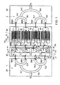
- Fig. 1 is a schematic view showing a plane pattern of a high frequency amplifier according to a first embodiment.
- Fig. 2 is a view showing a circuit of the high frequency amplifier of Fig. 1 .
- the high frequency amplifier according to the first embodiment is a power amplifier. As shown in Figs. 1 and 2 , the high frequency amplifier of the first embodiment is provided with an input circuit substrate 20, a matching circuit capacitor substrate 22, a semiconductor substrate 24 and an output circuit substrate 26. A division circuit 7 for distributing an input signal is formed on the input circuit substrate 20. A stabilization circuit substrate 21 is provided above the matching circuit capacitor substrate 22. Four RC parallel-connected circuits 9 for restraining a loop oscillation occurring between FET cells (unit cells) are formed on the stabilization circuit substrate 21. Four amplification elements (FETs) Q1-Q4 are formed on the semiconductor substrate 24. The amplification elements Q1-Q4 constitute the FET cells (unit cells) for amplifying signals divided from the division circuit 7, respectively.
- FETs amplification elements
- the amplification elements Q1-Q4 are discrete semiconductor devices.
- a combination circuit 8 which combines signals output from the amplification elements Q1-Q4 is formed on the output circuit substrate 26.
- the input circuit substrate 20, the matching circuit capacitor substrate 22, and the output circuit substrate 26 are a dielectric substrate.
- An input terminal Pi is formed on the input circuit substrate 20.
- the division circuit 7 includes two division lines SL1 and four division lines SL2.
- Each of the RC parallel-connected circuits 9 has a capacitor C and a resistor R connected with each other.
- An output terminal Po is arranged on the output circuit substrate 26.
- the combination circuit 8 includes four combination lines SL4 and two combination lines SL5.
- the division lines SL2 and electrodes 21a provided on the matching circuit capacitor substrate 22 are connected through bonding wires BW1 (shown as L1 in Fig. 2 ) respectively.
- Electrodes 21c provided on the stabilization circuit substrate 21 and gate electrodes G of the amplification elements Q1-Q4 are connected through bonding wires BW2 (shown as L2 in Fig. 2 ), respectively.
- Drain electrodes D of the amplification elements Q1-Q4 and the combination lines SL4 are connected through bonding wires BW3 (shown as L3 in Fig. 2 ), respectively.
- the RC parallel-connected circuits 9 are not arranged on the semiconductor substrate 24, but are arranged on the matching circuit capacitor substrate 22 other than the semiconductor substrate 24.
- the high frequency amplifier according to the first embodiment is provided with the four FET cells i.e. the amplification elements Q1-Q4 so as to obtain a large electric power.
- the input signal is divided by the division lines SL1, SL2 correspondingly to the number of the FET cells. Signals obtained through the division are amplified by the four amplification elements Q1-Q4 which constitute FET cells. Subsequently, the amplified signals are combined and outputted by the combination lines SL4 and SL5.
- an input signal of high frequency is input from the input terminal Pi, and the two division lines SL1 produce two signals from the input signal obtained from the input terminal Pi.
- Each set of two division lines SL2 produces two signal from one signal obtained from each division line SL1.
- Four signals obtained from the division lines SL2 are input to the gate electrodes G of the amplification elements Q1-Q4 respectively and are power-amplified.
- Each set of two combination lines SL4 which are connected to each set of two drain terminals D of the amplification elements Q1-Q4 combines each set of two signals power-amplified by the corresponding amplification elements to produce one signal.
- the two combination lines SL5 combines two signals obtained from the four combination lines SL4 to produce one signal.
- the output terminal Po outputs the signal obtained from the combination lines SL5 to outside.
- the RC parallel-connected circuits 9 which are included in the stabilization circuit 10 are arranged correspondingly to the respective FET cells.
- the RC parallel-connected circuits 9 are connected in series between the division lines SL2 and the gate electrodes G, respectively.
- the RC parallel-connected circuits 9 restrain oscillations which occur in a loop of adjacent FET cells and in a loop of non-adjacent (dispersed) FET cells, as described below.
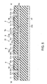
- Figs. 3 to 5 show sectional structures of a configuration including the matching circuit capacitor substrate 22 and the stabilization circuit substrate 21 which are used in the first embodiment.
- Fig. 3 is an enlarged view showing a section taken along a IV-IV line of Fig. 1 schematically.
- Fig. 4 is an enlarged view showing a section taken along a V-V line of Fig. 1 schematically.
- Fig. 5 is an enlarged view showing a section taken along a VI-VI line of Fig. 1 schematically.
- an electrode 21a is formed on a surface of the matching circuit capacitor substrate (a first dielectric substrate) 22, and a ground electrode 22a is formed on the other surface of the matching circuit capacitor substrate 22 opposite to the former surface.
- Each capacitor C1 shown in Fig. 2 is composed of the electrode 21a, the electrode 21c and the matching circuit capacitor substrate (the first dielectric substrate) 22.
- the stabilization circuit substrate (a second dielectric substrate) 21 on which the RC parallel-connected circuits 9 are formed is laminated on the electrode 21a.
- the resistor R i.e. a resistor layer 18 which is included in each RC parallel-connected circuit 9 and the electrode 21c arranged to connect electrically with an end of the resistor layer 18 are formed adjacently on the stabilization circuit substrate 21.
- a plurality of through holes TH is formed in the stabilization circuit substrate 21.
- each RC parallel-connected circuit 9 is composed of the electrode 21a, the electrode 21c and the stabilization circuit substrate (the second dielectric substrate) 21.
- NiCr nickel chrome alloy which has a sheet resistance of 50 ⁇ / ⁇
- the shape may be about 50 ⁇ m in width and about 30 ⁇ m in length.
- a capacitor having a capacitance value of about 0.5 to about 1.0 pF, for example, may be used.
- a specific example of the stabilization circuit substrate 21 for realizing such a capacitor C is shown in Table 1.
- alumina is employed for the material of the stabilization circuit substrate 21.
- the thickness is about 100 ⁇ m, and the two adjacent side lengths are about 1 mm respectively.
- Fig. 6 is an enlarged top view showing a portion J of one of the amplification elements Q1-Q4 of the high frequency amplifier according to the first embodiment shown in Fig. 1 .
- Fig. 7 is an enlarged view showing a section taken along a III-III line of Fig. 6 schematically.
- Fig. 7 shows a section of a High Electron Mobility Transistor (HEMT) adopted as the amplification elements Q1-Q4.
- HEMT High Electron Mobility Transistor
- each of the amplification elements Q1-Q4 is formed on a semiconductor portion 110 which is a part of the semiconductor substrate 24 of Fig. 1 .
- gate finger electrodes 124, source finger electrodes 120 and drain finger electrodes 122 are formed on a first surface of the semiconductor portion 110.
- Each group of the gate finger electrodes 124 is bundled by each of the gate electrodes G.
- Each group of the source finger electrodes 120 is bundled by each of the source electrodes S.
- Each group of the drain finger electrodes 122 is bundled by each of the drain electrodes D.
- Via-holes are formed in portions of the semiconductor substrate 24 under the source electrodes S.
- a ground electrode (not shown) is formed on a second surface of the semiconductor portion 110 opposite to the first surface.
- a barrier metal layer is formed on an inner wall of each via-hole, and a metal layer for filling each via-hole is formed on the barrier metal layer.
- the source electrodes S are connected to the ground electrode through the filled metal layer.
- the bonding wires BW2 are connected to the gate electrodes G respectively.
- the bonding wires BW3 are connected to the drain electrodes D respectively.
- the semiconductor substrate 24 or the semiconductor portion 110 may be any one of a GaAs substrate, a SiC substrate, a GaN substrate, a substrate including a SiC substrate on which a GaN epitaxial layer is formed, a substrate including a SiC substrate on which a hetero-junction epitaxial layer of GaN/AlGaN is formed, a sapphire substrate, or a diamond substrate.
- a compound-semiconductor layer 112 of a nitride series is formed on the semiconductor portion 110, and an aluminum gallium nitride layer (Al x Ga 1-x N) 118 is formed on the semiconductor layer 112.
- X is a value which satisfies 0.1 ⁇ x ⁇ 1.
- Each source finger electrode 120, each gate finger electrode 124 and each drain finger electrode 122 are formed on the semiconductor layer 118.
- a Two-Dimensional Electron Gas layer (2DEG layer) 116 is formed at an interface between the semiconductor layers 112, 118.
- Fig. 8 illustrates a view showing a loop LP1 between adjacent FET cells which is formed in the first embodiment.
- Fig. 9 illustrates a view showing a loop LP2 between non-adjacent (dispersed) FET cells which is formed in the first embodiment.
- the RC parallel-connected circuits 9 which is included in the stabilization circuit 10 are arranged between the division lines SL2 and the gate electrodes G of the amplification elements Q1-Q4 respectively so that the circuits 9 may correspond to the respective amplification elements Q1-Q4. In this case, any one of the waves of the loops passes through any one of the RC parallel-connected circuits 9.
- an oscillation which occurs in the loop LP2 of the non-adjacent (dispersed) FET cells shown in Fig. 9 can be restrained as well as an oscillation which occurs in the loop LP1 of the adjacent FET cells shown in Fig. 8 .
- the RC parallel-connected circuits 9 which are included in the stabilization circuit 10 are arranged not between the FET cells but are arranged correspondingly to the respective FET cells, a loop oscillation which is caused by any combination of the FET cells can be restrained effectively.
- Fig. 10 shows an example of a fundamental circuit configuration including a stabilization circuit of a high frequency amplifier according to a comparative example.
- the example is provided with input and output terminations 30, 31, an FET cell 32, an inductor 33 and a resistor 34.
- a gate of the FET cell 32 is connected to a series circuit including the inductor 33 and the resistor 34, and the gate is grounded via the series circuit.
- the terminations 30, 31 have an impedance of 50 ⁇ respectively
- the inductor 33 has an inductance of 0.156nH
- the resistor 34 has a resistance of 12.375 ⁇ .
- Fig. 11 shows an example of a fundamental circuit configuration including a stabilization circuit corresponding to the stabilization circuit of the high frequency amplifier according to the first embodiment.
- series resistors are used.
- the example is provided with input and output terminations 30, 31, a FET cell 32, a RC parallel-connected circuit 9 including a resistor 34 and a capacitor C.
- One ends of the input terminations 30, 31 are grounded respectively.
- the other end of the output termination 31 is connected to a drain of the FET cell 32.
- the RC parallel-connected circuit 9 is connected between a gate of the FET cell 32 and the other end of the input termination 30.
- the terminations 30, 31 have an impedance of 50 Q respectively
- the capacitor C has a capacitance of 0.85 pF
- the resistor R has a resistance of 30 ⁇ .
- the 10 , 11 can stabilize the high frequency amplifiers, which operate at 15 GHz, for example. Further, even when the high frequency amplifiers operate at 7 GHz or more, the stability factor can exceed one (1). This is because the frequency at which a loop oscillation is easy to occur is integral or 1/2 multiple of an operation frequency and thus a loop oscillation does not occur so far as the stability factor exceeds one (1) at a frequency higher than one half of the operation frequency.
- the resistor R is provided between the gate of the FET cell 32 and a ground terminal.
- the inductor 33 which has a large inductance
- the RC parallel-connected circuit 9 including the capacitor C and the resistor R is provided, as shown in Fig. 11 . Accordingly, the stabilization circuit of the first embodiment does not always need to arrange such an inductor as the inductor 33 of the stabilization circuit of the comparative example.
- the stabilization circuit of the comparative example needs grounding, it is necessary to provide a via-hole for forming an electrode in the via-hole, in a semiconductor substrate.
- the electrode is formed to connect the stabilization circuit with a ground electrode. But, since the stabilization circuit of the first embodiment does not always need grounding, the layout is easier.
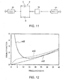
- Fig. 12 is a view for comparing stability factors of the stabilization circuit of the comparative example and the stabilization circuit of the first embodiment.
- a line m6 indicates a stability factor of a case where the stabilization circuit of the comparative example is used
- a line m5 indicates a stability factor of a case where the stabilization circuit of the first embodiment is used
- a line m2 indicates a stability factor of a case where any stabilization circuit is not used.
- stability factors at 7 GHz will be focused below.
- the stability factor of the case using the stabilization circuit of the comparative example is 1.840
- the stability factor of the case using the stabilization circuit of the first embodiment is 1.041.
- the stability factor of the case where any stabilization circuit is not used reaches one (1) at a frequency which exceeds 20 GHz nearly. Accordingly, as apparent from Fig. 12 , the stability factors of both of the cases which use the stabilization circuit of the comparative example and the stabilization circuit of the first embodiment exceed one (1) at a frequency higher than one half of the operation frequency (15 GHz) i.e. a frequency of about 7 GHz or more.
- the stability factor k can be one (1) or more at a frequency 1/2f.
- Fig. 13 is a view for comparing gains of the stabilization circuit of the comparative example and the stabilization circuit of the first embodiment.
- a line m3 indicates a gain of a case where the stabilization circuit of the comparative example is used
- a line m4 indicates a gain of a case where the stabilization circuit of the first embodiment is used
- a line m1 indicates a gain of a case where any stabilization circuit is not used.
- gains at 7 GHz will be focused below.
- the gain of the case using the stabilization circuit of the comparative example is 4.759 dB
- the gain of the case using the stabilization circuit of the first embodiment is 4.729 dB. Accordingly, as apparent from Fig.
- the gains of both of the cases that use the stabilization circuits of the comparative example and the first embodiment are lower only by approximately 1 dB than the gain (5.729 dB) of the case where any stabilization circuit is not used,.
- the RC parallel-connected circuits 9 which are included in the stabilization circuit 10 are arranged correspondingly to the respective FET cells.
- an oscillation which occurs in a loop of non-adjacent (dispersed) FET cells can be restrained as well as an oscillation which occurs in a loop of adjacent FET cells.
- the RC parallel-connected circuits 9 which are included in the stabilization circuit 10 are arranged not between the FET cells but are arranged correspondingly to the respective FET cell, a loop oscillation which is caused by any combination of the FET cells can be restrained effectively.
- the RC parallel-connected circuits 9 provided in the high frequency amplifier according to the first embodiment are connected in series between the division lines SL2 and the gate electrodes G of the amplification elements Q1-Q4. Further, the stabilization circuit substrate 21 is provided with the RC parallel-connected circuits 9 having the capacitor C and the resistor R respectively.
- the high frequency amplifier according to the first embodiment can be smaller than a high frequency amplifier having a stabilization circuit which includes a shunt resistor, and can secure almost the same stability factor and the same gain as a high frequency amplifiers which includes a shunt resistor.
- the high frequency amplifier becomes easy to be affected by an electrical influence which is caused by electromagnetic induction combination with a series coil of a matching circuit.
- the stabilization circuit substrate 21 includes the RC parallel-connected circuits 9 having the capacitor C and resistor R respectively, such electromagnetic induction combination is difficult to occur.
- Fig. 14 is a schematic view showing a plane pattern of a high frequency amplifier according to a second embodiment.
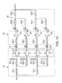
- Fig. 15 shows a circuit configuration of the high frequency amplifier of Fig. 14 .
- the high frequency power amplifier is provided with an input circuit substrate 19, a semiconductor substrate 24 and an output circuit substrate 26.
- a division circuit 7 and four RC parallel-connected circuits 9 are formed on the input circuit substrate 19.
- the division circuit 7 is provided with two division lines SL1 and four division lines SL2 which divides an input signal.
- the RC parallel-connected circuits 9 are included in a stabilization circuit 10 to restrain a loop oscillation which is caused between four FET cells as described below.
- An input terminal Pi, conductive lines 6a, 6b, and stub circuits ST are arranged on the input circuit substrate 19.
- Each of the RC parallel-connected circuits 9 is provided with a capacitor C and a resistor R which are connected in parallel with each other.
- the amplification elements Q1-Q4 which constitute the FET cells respectively are formed on the semiconductor substrate 24.
- the amplification elements Q1-Q4 amplify signals obtained by the division which is performed by the division circuit 7.
- Division lines SL3 are arranged on the semiconductor substrate 24.
- a combination circuit 8 is formed on the output circuit substrate 26.
- the combination circuit 8 is provided with four combination lines SL4 and two combination lines SL5, which combines outputs from the amplification elements Q1-Q4.
- An output terminal Po is arranged on the output circuit substrate 26.
- the input circuit substrate 19 and the output circuit substrate 26 are dielectric substrates.
- the division lines SL2 are connected with the conductive lines 6a respectively.
- the conductive lines 6b are connected with the division lines SL3 through bonding wires BW2 (shown as wires L2 in Fig. 15 ) respectively.
- the division lines SL3 are connected to gate electrodes G of the amplification elements Q1-Q4 respectively.
- Drain electrodes D of the amplification elements Q1-Q4 and the combination lines SL4 included in the division circuit 8 are connected through bonding wires BW3 (shown as wires L3 in Fig. 15 ) respectively.
- the stabilization circuit 10 which is provided with the RC parallel-connected circuits 9 having the capacitor C and the resistor R respectively is not arranged on the semiconductor substrate 24, but is arranged together with the division circuit 7 on the input circuit substrate 19 other than the semiconductor substrate 24.
- the high frequency amplifier according to the second embodiment is provided with the four FET cells i.e. the amplification elements Q1-Q4, so as to obtain a large electric power.
- the input signal is divided by the division lines SL1 and SL2, correspondingly to the number of the FET cells. Signals obtained by the division are amplified by the amplification elements Q1-Q4. The amplified signals are combined and outputted by the combination lines SL4 and SL5.
- an input signal of a high frequency is input from the input terminal Pi, and the two division lines SL1 produce two signals from the input signal obtained from the input terminal Pi.
- Each set of two division lines SL2 produces two signals from one signal obtained from each division lines SL1.
- Four signals obtained from the four division lines SL2 are input to the gate electrodes G of the amplification elements Q1-Q4 respectively through the division lines SL3 and are power-amplified.
- Each set of two combination lines SL4 which is connected to each set of two drain terminals D of the amplification elements Q1-Q4 combines each set of two signals which are power-amplified by each set of two amplification elements to produces one signal.
- the two combination lines SL5 combine two signals obtained from the combination lines SL4 to one signal.
- the output terminal Po outputs the signal obtained from the combination lines SL5 to outside.
- the stub circuits ST are connected respectively to transmission lines of the signals which are obtained from the division lines SL2 or to portions of the division lines SL2.
- the RC parallel-connected circuits 9 which are included in the stabilization circuit 10 are arranged between the division lines SL2 and the corresponding gate electrodes G of the amplification elements Q1-Q4, respectively.
- the RC parallel-connected circuits 9 have a resistor R and a capacitor C connected in parallel with each other, respectively.
- the resistor R and the capacitor C are mutually connected by the conductive lines 6a, 6b.
- the RC parallel-connected circuits 9 restrain an oscillation which occurs in a loop of adjacent FET cells composed of the amplification elements Q1-Q4 and an oscillation which occurs in a loop of non- adjacent (dispersed) FET cells.
- the stabilization circuit 10 is arranged not between the FET cells but is arranged correspondingly to all of the FET cells respectively, a loop oscillation which is caused by any combination of the FET cells can be restrained effectively.
- the stabilization circuit 10 provided in the high frequency amplifier according to the second embodiment is connected in series between the division line SL2 and the gate electrodes G of the amplification elements Q1-Q4.
- the stabilization circuit 10 is provided with the RC parallel-connected circuits 9 having the capacitor C and the resistor R respectively.
- the high frequency amplifier according to the second embodiment can be smaller than a high frequency amplifier using a stabilization circuit including a shunt resistor, and can secure almost the same stability factor and the same gain as the latter high frequency amplifier.
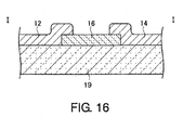
- Fig. 16 shows a configuration example of the resistor R included each RC parallel-connected circuit 9 in the second embodiment.
- Fig. 16 is an enlarged view showing a section taken along a I-I line of Fig. 14 schematically.
- the resistor R is composed of a resistor layer 16 arranged on a portion of the semiconductor substrate 19 between respective ends of electrodes 12, 14.
- the electrodes 12, 14 constitute the conductive lines 6a, 6b which are provided on the semiconductor substrate 19, respectively. Tip end portions of the electrodes 12, 14 are connected with the resistor layer 16 so as to extend over end portions of the resistor layer 16, respectively.
- the other end of the electrode 12 is connected with one of the division lines SL2, and the other end of the electrode 14 is connected with one of the division lines SL3.
- a resistor of about 30 ⁇ may be used as the resistor R.
- a specified example of the resistor layer 16 for realizing such a resistor of about 30 ⁇ is shown in Table 2.
- the material of the resistor is GaAs containing Si and the dose amount of Si is 4 ⁇ 10 13 /cm 2
- a line width of about 50 ⁇ m and a line length of about 20 ⁇ m may be adopted for the resistor layer.
- the material of the resistor is AlGaN/GaN where the Al composition rate of AlGaN is 25% and the thickness of AlGaN is 25 nm
- a line width of about 50 ⁇ m and a line length of about 4 ⁇ m may be adopted for the resistor layer.
- Table 2 MATERIAL OF RESISTOR LAYER 16 SHEET RESISTANCE ( ⁇ / ⁇ ) SIZE OF RESISTOR LAYER 16 LINE WIDTH ( ⁇ m) LINE LENGTH ( ⁇ m) GaAs (DOSE AMOUNT OF Si:4 ⁇ 10 13 /cm 2 ) 80 50 18.75 AlGaN/GaN (Al COMPOSITION RATE: 25%, THICKNESS: 25nm) 400 50 3.75
- Fig. 17 shows a configuration example of the capacitor C included in each RC parallel-connected circuit 9 in the second embodiment.
- Fig. 17 is an enlarged view showing a section taken along a II-II line of Fig. 14 schematically.
- the capacitor C has a MIM structure where the capacitor C is formed to have a structure which interposes an insulating layer 17 between the electrodes 12, 14 composing the conductive lines 6a, 6b.
- the capacitor C is formed of the electrodes 12a, 14a and the insulating layer 17.
- the electrodes 12a, 14a constitute the conductive lines 6a, 6b respectively and are arranged on the semiconductor substrate 19.
- the insulating layer 17 are arranged on a portion of the semiconductor substrate 19 between respective ends of electrodes 12a, 14a.
- the electrodes 12a is formed so as to extend over the insulating layer 17.
- the insulating layer 17 is formed so as to extend over the electrodes 14a. Accordingly, the capacitor C has a structure where the insulating layer 17 is sandwiched between the electrodes 12a, 14a.
- the other end of the electrode 12a is connected with one of the division lines SL2, and the other end of the electrode 14a is connected with one of the division lines SL3.
- a capacitor C of about 0.5 to 1.0 pF may be used, for example.
- a specified example of the insulating layer is shown in Table 3.
- the material of the insulating layer 17 is SiN having a thickness of 0.2 ⁇ m
- two adjacent side lengths may be about 50 ⁇ m and about 50 ⁇ m.
- the material of the insulating layer is SiO 2 having a thickness of about 0.1 ⁇ m
- two adjacent side lengths may be about 50 ⁇ m and about 50 ⁇ m.
- the amplification elements to be mounted on a high frequency amplifier are not limited to FETs or HEMTs.
- Laterally Diffused Metal-Oxide-Semiconductor (LDMOS) field effect transistors or hetero-junction bipolar transistors (HBTs) may be also used as the amplification elements.
- LDMOS Laterally Diffused Metal-Oxide-Semiconductor
- HBTs hetero-junction bipolar transistors
Landscapes
- Engineering & Computer Science (AREA)
- Power Engineering (AREA)
- Microelectronics & Electronic Packaging (AREA)
- Microwave Amplifiers (AREA)
- Amplifiers (AREA)
Abstract
Description
- Embodiments described herein relate generally to a high frequency amplifier.
- With higher performance of field effect transistors (hereinafter referred to as "FETs") which compose FET cells (unit cells) in a high frequency amplifier, the frequency of a loop oscillation of an odd mode becomes higher and the loop becomes smaller. As a result, the loop oscillation arises between the FET cells of the high frequency amplifier.
- In order to restrain such a loop oscillation occurring between FET cells, a technique of arranging a resistor (inter-cell resistor) at a suitable position between FET cells or a technique of arranging a resistor (shunt resistor) between a gate of an FET and a ground terminal has been applied.
- In a case of arranging a resistor between FET cells, an oscillation which occurs in a loop including adjacent FET cells may be effectively restrained, but an oscillation which occurs in a loop including non-adjacent (dispersed) FET cells may not be restrained effectively.
- In a case of arranging a resistor between a gate of an FET and a ground terminal, it is necessary to provide a large inductor in order to prevent deterioration of a high frequency characteristic such as leakage of a high frequency signal.
-
-
Fig. 1 is a schematic view showing a plane pattern of a high frequency amplifier according to a first embodiment. -
Fig. 2 is a view showing a circuit of the high frequency amplifier according to the first embodiment. -
Fig. 3 is an enlarged view showing a section taken along a IV-IV line ofFig. 1 schematically. -
Fig. 4 is an enlarged view showing a section taken along a V-V line ofFig. 1 schematically. -
Fig. 5 is an enlarged view showing a section taken along a VI-VI line ofFig. 1 schematically. -
Fig. 6 is an enlarged top view showing a portion J ofFig. 1 . -
Fig. 7 is an enlarged view showing a section taken along a III-III line ofFig. 6 schematically. -
Fig. 8 is a view showing a loop between adjacent FET cells. -
Fig. 9 is a view showing a loop between non-adjacent FET cells. -
Fig. 10 is a schematic circuit diagram of a high frequency amplifier having a stabilization circuit according to a comparative example. -
Fig. 11 is a schematic circuit diagram of a high frequency amplifier having a stabilization circuit according to the first embodiment. -
Fig. 12 is a view for comparing stability factors of the stabilization circuits according to the comparative example and the first embodiment. -
Fig. 13 is a view for comparing gains of the stabilization circuits according to the comparative example and the first embodiment. -
Fig. 14 is a schematic view showing a plane pattern of a high frequency amplifier according to a second embodiment. -
Fig. 15 is a view showing a circuit of the high frequency amplifier according to the second embodiment. -
Fig. 16 is an enlarged view showing a section taken along a I-I line ofFig. 14 schematically. -
Fig. 17 is an enlarged view showing a section taken along a II-II line ofFig. 14 schematically. - According to one embodiment, a high frequency amplifier having a division circuit, FET cells, a stabilization circuit and a combination circuit is provided. The division circuit divides an input signal to produce a plurality of signals. The FET cells amplify the signals produced by the division circuit. The stabilization circuit provided with RC parallel-connected circuits which are connected in series between the division circuit and gates of the FET cells respectively. Each of the RC parallel-connected circuits has a capacitor and a resistor connected in parallel with each other. The combination circuit combines the signals amplified by the FET cells.
- Hereinafter, further embodiments will be described with reference to the drawings.
- In the drawings, the same reference numerals denote the same or similar portions respectively.
- A first embodiment will be described with reference to
Figs. 1 and2 . -
Fig. 1 is a schematic view showing a plane pattern of a high frequency amplifier according to a first embodiment.Fig. 2 is a view showing a circuit of the high frequency amplifier ofFig. 1 . - The high frequency amplifier according to the first embodiment is a power amplifier. As shown in
Figs. 1 and2 , the high frequency amplifier of the first embodiment is provided with aninput circuit substrate 20, a matchingcircuit capacitor substrate 22, asemiconductor substrate 24 and anoutput circuit substrate 26. Adivision circuit 7 for distributing an input signal is formed on theinput circuit substrate 20. Astabilization circuit substrate 21 is provided above the matchingcircuit capacitor substrate 22. Four RC parallel-connectedcircuits 9 for restraining a loop oscillation occurring between FET cells (unit cells) are formed on thestabilization circuit substrate 21.
Four amplification elements (FETs) Q1-Q4 are formed on thesemiconductor substrate 24. The amplification elements Q1-Q4 constitute the FET cells (unit cells) for amplifying signals divided from thedivision circuit 7, respectively. The amplification elements Q1-Q4 are discrete semiconductor devices. Acombination circuit 8 which combines signals output from the amplification elements Q1-Q4 is formed on theoutput circuit substrate 26. Theinput circuit substrate 20, the matchingcircuit capacitor substrate 22, and theoutput circuit substrate 26 are a dielectric substrate. An input terminal Pi is formed on theinput circuit substrate 20. Thedivision circuit 7 includes two division lines SL1 and four division lines SL2. Each of the RC parallel-connectedcircuits 9 has a capacitor C and a resistor R connected with each other. An output terminal Po is arranged on theoutput circuit substrate 26. Thecombination circuit 8 includes four combination lines SL4 and two combination lines SL5.
The division lines SL2 andelectrodes 21a provided on the matchingcircuit capacitor substrate 22 are connected through bonding wires BW1 (shown as L1 inFig. 2 ) respectively.Electrodes 21c provided on thestabilization circuit substrate 21 and gate electrodes G of the amplification elements Q1-Q4 are connected through bonding wires BW2 (shown as L2 inFig. 2 ), respectively. Drain electrodes D of the amplification elements Q1-Q4 and the combination lines SL4 are connected through bonding wires BW3 (shown as L3 inFig. 2 ), respectively. As mentioned above, the RC parallel-connectedcircuits 9 are not arranged on thesemiconductor substrate 24, but are arranged on the matchingcircuit capacitor substrate 22 other than thesemiconductor substrate 24. - The high frequency amplifier according to the first embodiment is provided with the four FET cells i.e. the amplification elements Q1-Q4 so as to obtain a large electric power. The input signal is divided by the division lines SL1, SL2 correspondingly to the number of the FET cells. Signals obtained through the division are amplified by the four amplification elements Q1-Q4 which constitute FET cells. Subsequently, the amplified signals are combined and outputted by the combination lines SL4 and SL5.
- Specifically, an input signal of high frequency is input from the input terminal Pi, and the two division lines SL1 produce two signals from the input signal obtained from the input terminal Pi. Each set of two division lines SL2 produces two signal from one signal obtained from each division line SL1. Four signals obtained from the division lines SL2 are input to the gate electrodes G of the amplification elements Q1-Q4 respectively and are power-amplified. Each set of two combination lines SL4 which are connected to each set of two drain terminals D of the amplification elements Q1-Q4 combines each set of two signals power-amplified by the corresponding amplification elements to produce one signal. Further, the two combination lines SL5 combines two signals obtained from the four combination lines SL4 to produce one signal. The output terminal Po outputs the signal obtained from the combination lines SL5 to outside.
- As mentioned above, according to the embodiment, the RC parallel-
connected circuits 9 which are included in thestabilization circuit 10 are arranged correspondingly to the respective FET cells. The RC parallel-connected circuits 9 are connected in series between the division lines SL2 and the gate electrodes G, respectively. The RC parallel-connected circuits 9 restrain oscillations which occur in a loop of adjacent FET cells and in a loop of non-adjacent (dispersed) FET cells, as described below. -
Figs. 3 to 5 show sectional structures of a configuration including the matchingcircuit capacitor substrate 22 and thestabilization circuit substrate 21 which are used in the first embodiment.Fig. 3 is an enlarged view showing a section taken along a IV-IV line ofFig. 1 schematically.Fig. 4 is an enlarged view showing a section taken along a V-V line ofFig. 1 schematically.Fig. 5 is an enlarged view showing a section taken along a VI-VI line ofFig. 1 schematically.
InFigs. 3 to 5 , anelectrode 21a is formed on a surface of the matching circuit capacitor substrate (a first dielectric substrate) 22, and aground electrode 22a is formed on the other surface of the matchingcircuit capacitor substrate 22 opposite to the former surface. Each capacitor C1 shown inFig. 2 is composed of theelectrode 21a, theelectrode 21c and the matching circuit capacitor substrate (the first dielectric substrate) 22. The stabilization circuit substrate (a second dielectric substrate) 21 on which the RC parallel-connected circuits 9 are formed is laminated on theelectrode 21a.
As shown inFig. 5 , the resistor R i.e. aresistor layer 18 which is included in each RC parallel-connectedcircuit 9 and theelectrode 21c arranged to connect electrically with an end of theresistor layer 18 are formed adjacently on thestabilization circuit substrate 21. As shown inFigs. 1 and5 , a plurality of through holes TH is formed in thestabilization circuit substrate 21. The other end of theresistor layer 18 and theelectrode 21a are electrically connected via anelectrode 21b formed in each through hole TH. The capacitor C of each RC parallel-connectedcircuit 9 is composed of theelectrode 21a, theelectrode 21c and the stabilization circuit substrate (the second dielectric substrate) 21. - For the matching
circuit capacitor substrate 22, a dielectric material of a high permittivity of K= 140, for example, may be employed, and, in this case, the thickness may be formed to be about 0.1 mm. For thestabilization circuit substrate 21, an alumina of K=10, for example, may be employed, and, in this case, the thickness may be formed to be about 0.1 mm. - For the
resistor layer 18, a nickel chrome alloy (NiCr) which has a sheet resistance of 50 Ω/□ may be employed, and, in this case, the shape may be about 50 µm in width and about 30 µm in length. - For the capacitor C, a capacitor having a capacitance value of about 0.5 to about 1.0 pF, for example, may be used. A specific example of the
stabilization circuit substrate 21 for realizing such a capacitor C is shown in Table 1. In order to obtain a capacitance of 0.85 pF, in the example, alumina is employed for the material of thestabilization circuit substrate 21. In this case, the thickness is about 100 µm, and the two adjacent side lengths are about 1 mm respectively.Table 1 MATERIAL OF STABILIZATION CIRCUIT SUBSTRATE 21RELATIVE PERMITTIVITY FILM THICKNESS (µm) AREA (mm2) LENGTHS OF ADJACENT SIDES (mm) FIRST SIDE SECOND SIDE ALUMINA 10 100 0.96 0.979796 0.979796 -
Fig. 6 is an enlarged top view showing a portion J of one of the amplification elements Q1-Q4 of the high frequency amplifier according to the first embodiment shown inFig. 1 .Fig. 7 is an enlarged view showing a section taken along a III-III line ofFig. 6 schematically.Fig. 7 shows a section of a High Electron Mobility Transistor (HEMT) adopted as the amplification elements Q1-Q4. - As shown in
Figs 1 ,6 , each of the amplification elements Q1-Q4 is formed on asemiconductor portion 110 which is a part of thesemiconductor substrate 24 ofFig. 1 . On a first surface of thesemiconductor portion 110,gate finger electrodes 124,source finger electrodes 120 and drainfinger electrodes 122 are formed. Each group of thegate finger electrodes 124 is bundled by each of the gate electrodes G. Each group of thesource finger electrodes 120 is bundled by each of the source electrodes S. Each group of thedrain finger electrodes 122 is bundled by each of the drain electrodes D.
Via-holes (not shown) are formed in portions of thesemiconductor substrate 24 under the source electrodes S. Further, a ground electrode (not shown) is formed on a second surface of thesemiconductor portion 110 opposite to the first surface. A barrier metal layer is formed on an inner wall of each via-hole, and a metal layer for filling each via-hole is formed on the barrier metal layer. The source electrodes S are connected to the ground electrode through the filled metal layer. - The bonding wires BW2 are connected to the gate electrodes G respectively. The bonding wires BW3 are connected to the drain electrodes D respectively.
- The
semiconductor substrate 24 or thesemiconductor portion 110 may be any one of a GaAs substrate, a SiC substrate, a GaN substrate, a substrate including a SiC substrate on which a GaN epitaxial layer is formed, a substrate including a SiC substrate on which a hetero-junction epitaxial layer of GaN/AlGaN is formed, a sapphire substrate, or a diamond substrate. - As shown in
Fig. 7 , a compound-semiconductor layer 112 of a nitride series is formed on thesemiconductor portion 110, and an aluminum gallium nitride layer (AlxGa1-xN) 118 is formed on the semiconductor layer 112. X is a value which satisfies 0.1≦x≦1. Eachsource finger electrode 120, eachgate finger electrode 124 and eachdrain finger electrode 122 are formed on thesemiconductor layer 118. A Two-Dimensional Electron Gas layer (2DEG layer) 116 is formed at an interface between the semiconductor layers 112, 118. -
Fig. 8 illustrates a view showing a loop LP1 between adjacent FET cells which is formed in the first embodiment.Fig. 9 illustrates a view showing a loop LP2 between non-adjacent (dispersed) FET cells which is formed in the first embodiment. In the high frequency amplifier according to the first embodiment, as shown inFig. 1 , the RC parallel-connected circuits 9 which is included in thestabilization circuit 10 are arranged between the division lines SL2 and the gate electrodes G of the amplification elements Q1-Q4 respectively so that thecircuits 9 may correspond to the respective amplification elements Q1-Q4.
In this case, any one of the waves of the loops passes through any one of the RC parallel-connected circuits 9. Thus, according to the high frequency amplifier of the first embodiment, an oscillation which occurs in the loop LP2 of the non-adjacent (dispersed) FET cells shown inFig. 9 can be restrained as well as an oscillation which occurs in the loop LP1 of the adjacent FET cells shown inFig. 8 . According to the high frequency amplifier of the first embodiment, since the RC parallel-connected circuits 9 which are included in thestabilization circuit 10 are arranged not between the FET cells but are arranged correspondingly to the respective FET cells, a loop oscillation which is caused by any combination of the FET cells can be restrained effectively. -
Fig. 10 shows an example of a fundamental circuit configuration including a stabilization circuit of a high frequency amplifier according to a comparative example. The example is provided with input andoutput terminations FET cell 32, aninductor 33 and aresistor 34. A gate of theFET cell 32 is connected to a series circuit including theinductor 33 and theresistor 34, and the gate is grounded via the series circuit. For example, theterminations inductor 33 has an inductance of 0.156nH, and theresistor 34 has a resistance of 12.375 Ω.
Fig. 11 shows an example of a fundamental circuit configuration including a stabilization circuit corresponding to the stabilization circuit of the high frequency amplifier according to the first embodiment. In the example, series resistors are used. Specifically, the example is provided with input andoutput terminations FET cell 32, a RC parallel-connectedcircuit 9 including aresistor 34 and a capacitor C. One ends of theinput terminations output termination 31 is connected to a drain of theFET cell 32. The RC parallel-connectedcircuit 9 is connected between a gate of theFET cell 32 and the other end of theinput termination 30. For example, theterminations
The stabilization circuits shown inFigs. 10 ,11 can stabilize the high frequency amplifiers, which operate at 15 GHz, for example. Further, even when the high frequency amplifiers operate at 7 GHz or more, the stability factor can exceed one (1). This is because the frequency at which a loop oscillation is easy to occur is integral or 1/2 multiple of an operation frequency and thus a loop oscillation does not occur so far as the stability factor exceeds one (1) at a frequency higher than one half of the operation frequency. - In the stabilization circuit of the comparative example shown in
Fig. 10 , the resistor R is provided between the gate of theFET cell 32 and a ground terminal. In order to prevent deterioration of a high frequency characteristic i.e. leakage of a high frequency signal, it is necessary to arrange theinductor 33, which has a large inductance, in the circuit configuration ofFig. 10 . On the other hand, in the circuit configuration including the stabilization circuit corresponding to the stabilization circuit of the first embodiment, which is formed to have series resistors, the RC parallel-connectedcircuit 9 including the capacitor C and the resistor R is provided, as shown inFig. 11 . Accordingly, the stabilization circuit of the first embodiment does not always need to arrange such an inductor as theinductor 33 of the stabilization circuit of the comparative example. - Since the stabilization circuit of the comparative example needs grounding, it is necessary to provide a via-hole for forming an electrode in the via-hole, in a semiconductor substrate. The electrode is formed to connect the stabilization circuit with a ground electrode. But, since the stabilization circuit of the first embodiment does not always need grounding, the layout is easier.
-
Fig. 12 is a view for comparing stability factors of the stabilization circuit of the comparative example and the stabilization circuit of the first embodiment. InFig. 12 , a line m6 indicates a stability factor of a case where the stabilization circuit of the comparative example is used, a line m5 indicates a stability factor of a case where the stabilization circuit of the first embodiment is used, and a line m2 indicates a stability factor of a case where any stabilization circuit is not used. For example, stability factors at 7 GHz will be focused below. The stability factor of the case using the stabilization circuit of the comparative example is 1.840, and the stability factor of the case using the stabilization circuit of the first embodiment is 1.041. On the other hand, the stability factor of the case where any stabilization circuit is not used reaches one (1) at a frequency which exceeds 20 GHz nearly. Accordingly, as apparent fromFig. 12 , the stability factors of both of the cases which use the stabilization circuit of the comparative example and the stabilization circuit of the first embodiment exceed one (1) at a frequency higher than one half of the operation frequency (15 GHz) i.e. a frequency of about 7 GHz or more. When an operation frequency is expressed as "f" and a stability factor is expressed as "k", the stability factor k can be one (1) or more at afrequency 1/2f. -
Fig. 13 is a view for comparing gains of the stabilization circuit of the comparative example and the stabilization circuit of the first embodiment. InFig. 13 , a line m3 indicates a gain of a case where the stabilization circuit of the comparative example is used, a line m4 indicates a gain of a case where the stabilization circuit of the first embodiment is used, and a line m1 indicates a gain of a case where any stabilization circuit is not used. For example, gains at 7 GHz will be focused below. The gain of the case using the stabilization circuit of the comparative example is 4.759 dB, and the gain of the case using the stabilization circuit of the first embodiment is 4.729 dB. Accordingly, as apparent fromFig. 13 , at an operation frequency of 15 GHz, the gains of both of the cases that use the stabilization circuits of the comparative example and the first embodiment are lower only by approximately 1 dB than the gain (5.729 dB) of the case where any stabilization circuit is not used,. - As explained above, according to the high frequency amplifier of the first embodiment, the RC parallel-
connected circuits 9 which are included in thestabilization circuit 10 are arranged correspondingly to the respective FET cells. Thus, an oscillation which occurs in a loop of non-adjacent (dispersed) FET cells can be restrained as well as an oscillation which occurs in a loop of adjacent FET cells. According to the high frequency amplifier of the first embodiment, since the RC parallel-connected circuits 9 which are included in thestabilization circuit 10 are arranged not between the FET cells but are arranged correspondingly to the respective FET cell, a loop oscillation which is caused by any combination of the FET cells can be restrained effectively. - The RC parallel-
connected circuits 9 provided in the high frequency amplifier according to the first embodiment are connected in series between the division lines SL2 and the gate electrodes G of the amplification elements Q1-Q4. Further, thestabilization circuit substrate 21 is provided with the RC parallel-connected circuits 9 having the capacitor C and the resistor R respectively. Thus, the high frequency amplifier according to the first embodiment can be smaller than a high frequency amplifier having a stabilization circuit which includes a shunt resistor, and can secure almost the same stability factor and the same gain as a high frequency amplifiers which includes a shunt resistor. - Further, in a case of a discrete type high frequency amplifier, when a shunt coil is used in order to constitute a stabilization circuit by a shunt resistor as in the comparative example, the high frequency amplifier becomes easy to be affected by an electrical influence which is caused by electromagnetic induction combination with a series coil of a matching circuit. However, according to the high frequency amplifier of the first embodiment, since the
stabilization circuit substrate 21 includes the RC parallel-connected circuits 9 having the capacitor C and resistor R respectively, such electromagnetic induction combination is difficult to occur. -
Fig. 14 is a schematic view showing a plane pattern of a high frequency amplifier according to a second embodiment.Fig. 15 shows a circuit configuration of the high frequency amplifier ofFig. 14 . - As shown in
Fig. 14 , the high frequency power amplifier according to the second embodiment is provided with aninput circuit substrate 19, asemiconductor substrate 24 and anoutput circuit substrate 26. Adivision circuit 7 and four RC parallel-connected circuits 9 are formed on theinput circuit substrate 19. Thedivision circuit 7 is provided with two division lines SL1 and four division lines SL2 which divides an input signal. The RC parallel-connected circuits 9 are included in astabilization circuit 10 to restrain a loop oscillation which is caused between four FET cells as described below. An input terminal Pi,conductive lines input circuit substrate 19. Each of the RC parallel-connected circuits 9 is provided with a capacitor C and a resistor R which are connected in parallel with each other.
Four amplification elements Q1-Q4 which constitute the FET cells respectively are formed on thesemiconductor substrate 24. The amplification elements Q1-Q4 amplify signals obtained by the division which is performed by thedivision circuit 7. Division lines SL3 are arranged on thesemiconductor substrate 24. Acombination circuit 8 is formed on theoutput circuit substrate 26. Thecombination circuit 8 is provided with four combination lines SL4 and two combination lines SL5, which combines outputs from the amplification elements Q1-Q4. An output terminal Po is arranged on theoutput circuit substrate 26. Theinput circuit substrate 19 and theoutput circuit substrate 26 are dielectric substrates.
The division lines SL2 are connected with theconductive lines 6a respectively. Theconductive lines 6b are connected with the division lines SL3 through bonding wires BW2 (shown as wires L2 inFig. 15 ) respectively. The division lines SL3 are connected to gate electrodes G of the amplification elements Q1-Q4 respectively. Drain electrodes D of the amplification elements Q1-Q4 and the combination lines SL4 included in thedivision circuit 8 are connected through bonding wires BW3 (shown as wires L3 inFig. 15 ) respectively. In the high frequency power amplifier according to the second embodiment, thestabilization circuit 10 which is provided with the RC parallel-connected circuits 9 having the capacitor C and the resistor R respectively is not arranged on thesemiconductor substrate 24, but is arranged together with thedivision circuit 7 on theinput circuit substrate 19 other than thesemiconductor substrate 24. - The high frequency amplifier according to the second embodiment is provided with the four FET cells i.e. the amplification elements Q1-Q4, so as to obtain a large electric power. The input signal is divided by the division lines SL1 and SL2, correspondingly to the number of the FET cells. Signals obtained by the division are amplified by the amplification elements Q1-Q4. The amplified signals are combined and outputted by the combination lines SL4 and SL5.
- Specifically, an input signal of a high frequency is input from the input terminal Pi, and the two division lines SL1 produce two signals from the input signal obtained from the input terminal Pi. Each set of two division lines SL2 produces two signals from one signal obtained from each division lines SL1. Four signals obtained from the four division lines SL2 are input to the gate electrodes G of the amplification elements Q1-Q4 respectively through the division lines SL3 and are power-amplified. Each set of two combination lines SL4 which is connected to each set of two drain terminals D of the amplification elements Q1-Q4 combines each set of two signals which are power-amplified by each set of two amplification elements to produces one signal. Further, the two combination lines SL5 combine two signals obtained from the combination lines SL4 to one signal. The output terminal Po outputs the signal obtained from the combination lines SL5 to outside. As shown in
Fig. 15 , the stub circuits ST are connected respectively to transmission lines of the signals which are obtained from the division lines SL2 or to portions of the division lines SL2. - The RC parallel-
connected circuits 9 which are included in thestabilization circuit 10 are arranged between the division lines SL2 and the corresponding gate electrodes G of the amplification elements Q1-Q4, respectively. The RC parallel-connected circuits 9 have a resistor R and a capacitor C connected in parallel with each other, respectively. The resistor R and the capacitor C are mutually connected by theconductive lines connected circuits 9 restrain an oscillation which occurs in a loop of adjacent FET cells composed of the amplification elements Q1-Q4 and an oscillation which occurs in a loop of non- adjacent (dispersed) FET cells. - According to the high frequency amplifier of the second embodiment, since the
stabilization circuit 10 is arranged not between the FET cells but is arranged correspondingly to all of the FET cells respectively, a loop oscillation which is caused by any combination of the FET cells can be restrained effectively. - The
stabilization circuit 10 provided in the high frequency amplifier according to the second embodiment is connected in series between the division line SL2 and the gate electrodes G of the amplification elements Q1-Q4. Thestabilization circuit 10 is provided with the RC parallel-connected circuits 9 having the capacitor C and the resistor R respectively. - Accordingly, the high frequency amplifier according to the second embodiment can be smaller than a high frequency amplifier using a stabilization circuit including a shunt resistor, and can secure almost the same stability factor and the same gain as the latter high frequency amplifier.
-
Fig. 16 shows a configuration example of the resistor R included each RC parallel-connectedcircuit 9 in the second embodiment.Fig. 16 is an enlarged view showing a section taken along a I-I line ofFig. 14 schematically.
The resistor R is composed of aresistor layer 16 arranged on a portion of thesemiconductor substrate 19 between respective ends ofelectrodes electrodes conductive lines semiconductor substrate 19, respectively. Tip end portions of theelectrodes resistor layer 16 so as to extend over end portions of theresistor layer 16, respectively. The other end of theelectrode 12 is connected with one of the division lines SL2, and the other end of theelectrode 14 is connected with one of the division lines SL3. - For example, a resistor of about 30 Ω may be used as the resistor R. A specified example of the
resistor layer 16 for realizing such a resistor of about 30 Ω is shown in Table 2. When the material of the resistor is GaAs containing Si and the dose amount of Si is 4×10¹³/cm2, a line width of about 50µm and a line length of about 20µm may be adopted for the resistor layer. Further, when the material of the resistor is AlGaN/GaN where the Al composition rate of AlGaN is 25% and the thickness of AlGaN is 25 nm, a line width of about 50µm and a line length of about 4µm may be adopted for the resistor layer.Table 2 MATERIAL OF RESISTOR LAYER 16SHEET RESISTANCE (Ω/□) SIZE OF RESISTOR LAYER 16LINE WIDTH (µm) LINE LENGTH (µm) GaAs (DOSE AMOUNT OF Si:4×10¹³/cm2) 80 50 18.75 AlGaN/GaN (Al COMPOSITION RATE: 25%, THICKNESS: 25nm) 400 50 3.75 -
Fig. 17 shows a configuration example of the capacitor C included in each RC parallel-connectedcircuit 9 in the second embodiment.Fig. 17 is an enlarged view showing a section taken along a II-II line ofFig. 14 schematically. The capacitor C has a MIM structure where the capacitor C is formed to have a structure which interposes an insulatinglayer 17 between theelectrodes conductive lines electrodes layer 17. Theelectrodes conductive lines semiconductor substrate 19. The insulatinglayer 17 are arranged on a portion of thesemiconductor substrate 19 between respective ends ofelectrodes electrodes 12a is formed so as to extend over the insulatinglayer 17. The insulatinglayer 17 is formed so as to extend over theelectrodes 14a. Accordingly, the capacitor C has a structure where the insulatinglayer 17 is sandwiched between theelectrodes electrode 12a is connected with one of the division lines SL2, and the other end of theelectrode 14a is connected with one of the division lines SL3. - For the capacitor C, a capacitor C of about 0.5 to 1.0 pF may be used, for example. A specified example of the insulating layer is shown in Table 3. When the material of the insulating
layer 17 is SiN having a thickness of 0.2µm, two adjacent side lengths may be about 50 µm and about 50 µm. When the material of the insulating layer is SiO2 having a thickness of about 0.1 µm, two adjacent side lengths may be about 50 µm and about 50 µm.Table 3 MATERIAL OF DIELECTRIC LAYER 17RELATIVE PERMITTIVITY FILM THICKNESS (µm) AREA (mm2) LENGTHS OF ADJACENT SIDES (mm) FIRST SIDE SECOND SIDE SiN 7 0.2 0.0027 0.0027 50 SiO2 3.9 0.1 0.0024 0.04899 50 - While high-frequency amplifiers according to certain embodiments have been described above, these embodiments have been presented by way of example only, and are not intended to limit the scope of the inventions. Indeed, the novel embodiments described herein may be embodied in a variety of other forms; furthermore, various omissions, substitutions and changes in the form of the embodiments described herein may be made without departing from the spirit of the inventions. The accompanying claims and their equivalents are intended to cover such forms or modifications as would fall within the scope and spirit of the inventions.
- For example, the amplification elements to be mounted on a high frequency amplifier are not limited to FETs or HEMTs. Laterally Diffused Metal-Oxide-Semiconductor (LDMOS) field effect transistors or hetero-junction bipolar transistors (HBTs) may be also used as the amplification elements.
Claims (10)
- A high frequency amplifier, comprising:a division circuit which divides an input signal to produce a plurality of signals;FET cells which amplifies signals produced by the division circuit;a stabilization circuit provided with RC parallel-connected circuits which are respectively connected in series between the division circuit and gates of the FET cells, each of the RC parallel-connected circuits having a capacitor and a resistor connected in parallel with each other; anda combination circuit which combines signals amplified by the FET cells.
- A high frequency amplifier according to Claim 1, wherein each of the FET cells and each of the RC parallel-connected circuits are connected with each other through a wire, respectively.
- A high frequency amplifier according to Claim 1, wherein the stabilization circuit is arranged on a substrate other than a semiconductor substrate on which the FET cells are arranged.
- A high frequency amplifier according to Claim 1, wherein the division circuit, the stabilization circuit and the combination circuit are respectively arranged on substrates other than a semiconductor substrate on which the FET cells are arranged.
- A high frequency amplifier according to Claim 4, wherein the division circuit and the stabilization circuit are arranged on the same substrate other than a semiconductor substrate on which the FET cells are arranged.
- A high frequency amplifier according to Claim 4, wherein the stabilization circuit includes:a circuit substrate of a dielectric material;a first electrode formed on the circuit substrate;a dielectric layer formed on the first electrode, the resistor being formed on the dielectric layer;a second electrode formed on the dielectric layer to compose the capacitor with the first electrode and the dielectric layer; anda third electrode formed in a through hole which is provided in the dielectric layer and connects the first electrode with the resistor electrically.
- A high frequency amplifier according to Claim 5, wherein the stabilization circuit includes:a circuit substrate of a dielectric material;a resistor formed on the circuit substrate;a capacitor formed on the circuit substrate, the capacitor having a first electrode, a dielectric layer formed on the first electrode, and a second electrode formed on the dielectric layer;a first conductive line which connects an end of the resistor and the first electrode electrically; anda second conductive line which connects the other end of the resistor and the second electrode electrically.
- A high frequency amplifier according to Claim 3, wherein the substrate other than the semiconductor substrate is a dielectric substrate.
- A high frequency amplifier according to Claim 4, wherein the substrate other than the semiconductor substrate is a dielectric substrate.
- A high frequency amplifier according to Claim 5, wherein the substrate other than the semiconductor substrate is a dielectric substrate.
Applications Claiming Priority (1)
| Application Number | Priority Date | Filing Date | Title |
|---|---|---|---|
| JP2011250470A JP5487187B2 (en) | 2011-11-16 | 2011-11-16 | High frequency amplifier |
Publications (2)
| Publication Number | Publication Date |
|---|---|
| EP2595313A1 true EP2595313A1 (en) | 2013-05-22 |
| EP2595313B1 EP2595313B1 (en) | 2018-05-02 |
Family
ID=46690395
Family Applications (1)
| Application Number | Title | Priority Date | Filing Date |
|---|---|---|---|
| EP12178610.7A Active EP2595313B1 (en) | 2011-11-16 | 2012-07-31 | High frequency amplifier |
Country Status (6)
| Country | Link |
|---|---|
| US (1) | US8786369B2 (en) |
| EP (1) | EP2595313B1 (en) |
| JP (1) | JP5487187B2 (en) |
| KR (1) | KR101419121B1 (en) |
| CN (1) | CN103117716B (en) |
| TW (1) | TWI517560B (en) |
Families Citing this family (12)
| Publication number | Priority date | Publication date | Assignee | Title |
|---|---|---|---|---|
| JP5711778B2 (en) | 2013-03-06 | 2015-05-07 | 株式会社東芝 | Semiconductor device |
| JP6203103B2 (en) | 2014-03-31 | 2017-09-27 | 株式会社東芝 | High frequency semiconductor device |
| JP6596841B2 (en) | 2015-02-25 | 2019-10-30 | 三菱電機株式会社 | Semiconductor device |
| JP6426498B2 (en) * | 2015-02-26 | 2018-11-21 | 株式会社東芝 | High frequency semiconductor device |
| JP6702083B2 (en) * | 2016-08-23 | 2020-05-27 | 株式会社村田製作所 | High frequency amplifier module |
| CN112154603B (en) * | 2018-05-28 | 2024-09-20 | 三菱电机株式会社 | Amplifier |
| US12224714B1 (en) | 2020-05-15 | 2025-02-11 | AmpliTech, Inc. | Multiple transistor low noise amplifier optimized for cryogenic temperatures |
| US12212287B1 (en) | 2020-05-15 | 2025-01-28 | AmpliTech, Inc. | Low noise amplifiers/front-ends optimized for use in 5G networks |
| US12231091B1 (en) * | 2020-05-15 | 2025-02-18 | AmpliTech, Inc. | Multiple transistor LNA MMIC design |
| WO2022138001A1 (en) | 2020-12-21 | 2022-06-30 | 株式会社村田製作所 | High-frequency circuit, high-frequency module, and communication device |
| JP7625346B2 (en) * | 2021-02-08 | 2025-02-03 | 三菱電機ディフェンス&スペーステクノロジーズ株式会社 | Stabilization circuit |
| JP7669975B2 (en) * | 2022-04-22 | 2025-04-30 | 三菱電機株式会社 | Semiconductor Device |
Citations (3)
| Publication number | Priority date | Publication date | Assignee | Title |
|---|---|---|---|---|
| US6232840B1 (en) * | 1999-06-10 | 2001-05-15 | Raytheon Company | Transistor amplifier having reduced parasitic oscillations |
| JP2005216943A (en) * | 2004-01-27 | 2005-08-11 | Murata Mfg Co Ltd | Semiconductor device and power amplifier using it |
| US20070118776A1 (en) * | 2005-11-22 | 2007-05-24 | Mitsubishi Electric Corporation | Power amplifier |
Family Cites Families (10)
| Publication number | Priority date | Publication date | Assignee | Title |
|---|---|---|---|---|
| JPS63283203A (en) * | 1987-05-15 | 1988-11-21 | Nec Corp | Power distribution circuit |
| JPH04361404A (en) * | 1991-06-10 | 1992-12-15 | Nec Corp | High frequency matching circuit |
| JPH1083998A (en) * | 1996-09-09 | 1998-03-31 | Mitsubishi Electric Corp | Semiconductor device |
| US6342815B1 (en) * | 2000-10-04 | 2002-01-29 | Trw Inc. | Manufacturable HBT power distributed amplifier for wideband telecommunications |
| JP4361313B2 (en) | 2003-05-08 | 2009-11-11 | 三菱電機株式会社 | High frequency power amplifier |
| JP4155326B2 (en) * | 2004-11-29 | 2008-09-24 | 株式会社村田製作所 | Semiconductor device and power amplifier |
| WO2007119266A1 (en) * | 2006-03-22 | 2007-10-25 | Fujitsu Limited | High frequency/high output amplifier |
| JP5224651B2 (en) * | 2006-03-31 | 2013-07-03 | Jx日鉱日石エネルギー株式会社 | Solid oxide fuel cell |
| US7525385B2 (en) * | 2006-10-30 | 2009-04-28 | Avago Technologies Wireless Ip (Singapore) Pte. Ltd. | Common drain driven cascode enhancement mode traveling wave amplifier |
| JP5238633B2 (en) | 2009-07-27 | 2013-07-17 | 株式会社東芝 | Semiconductor device |
-
2011
- 2011-11-16 JP JP2011250470A patent/JP5487187B2/en not_active Expired - Fee Related
-
2012
- 2012-07-25 US US13/557,609 patent/US8786369B2/en not_active Expired - Fee Related
- 2012-07-31 EP EP12178610.7A patent/EP2595313B1/en active Active
- 2012-08-03 TW TW101127982A patent/TWI517560B/en not_active IP Right Cessation
- 2012-08-08 CN CN201210280751.4A patent/CN103117716B/en active Active
- 2012-08-08 KR KR1020120086632A patent/KR101419121B1/en not_active Expired - Fee Related
Patent Citations (3)
| Publication number | Priority date | Publication date | Assignee | Title |
|---|---|---|---|---|
| US6232840B1 (en) * | 1999-06-10 | 2001-05-15 | Raytheon Company | Transistor amplifier having reduced parasitic oscillations |
| JP2005216943A (en) * | 2004-01-27 | 2005-08-11 | Murata Mfg Co Ltd | Semiconductor device and power amplifier using it |
| US20070118776A1 (en) * | 2005-11-22 | 2007-05-24 | Mitsubishi Electric Corporation | Power amplifier |
Also Published As
| Publication number | Publication date |
|---|---|
| US8786369B2 (en) | 2014-07-22 |
| EP2595313B1 (en) | 2018-05-02 |
| CN103117716A (en) | 2013-05-22 |
| TWI517560B (en) | 2016-01-11 |
| US20130120069A1 (en) | 2013-05-16 |
| TW201322624A (en) | 2013-06-01 |
| CN103117716B (en) | 2016-05-18 |
| JP5487187B2 (en) | 2014-05-07 |
| JP2013106293A (en) | 2013-05-30 |
| KR20130054120A (en) | 2013-05-24 |
| KR101419121B1 (en) | 2014-07-11 |
Similar Documents
| Publication | Publication Date | Title |
|---|---|---|
| EP2595313B1 (en) | High frequency amplifier | |
| EP2458730B1 (en) | Radiofrequency amplifier | |
| CN108233881B (en) | Amplifier circuit and packaged amplifier circuit | |
| JP7242777B2 (en) | High-power MMIC device with bypass-gated transistors | |
| EP3867950B1 (en) | Transistor level input and output harmonic terminations | |
| US9871501B2 (en) | RF circuit with multiple-definition RF substrate and conductive material void under a bias line | |
| US10211170B2 (en) | Power transistor with harmonic control | |
| US20160322942A1 (en) | Improved matching techniques for wide-bandgap power transistors | |
| EP3213411B1 (en) | Output matching network having a single combined series and shunt capacitor component | |
| US7859341B2 (en) | Semiconductor device | |
| US9923526B1 (en) | Harmonic filter for RF amplifier | |
| US9503035B2 (en) | High-frequency amplifier | |
| JP2013182993A (en) | Semiconductor device | |
| JP7717552B2 (en) | Semiconductor Devices | |
| WO2025197830A1 (en) | Doherty amplifier | |
| WO2025179811A1 (en) | Power amplifier, power amplifier link, radio frequency front-end circuit and electronic device | |
| JP2007324422A (en) | Semiconductor device and manufacturing method thereof | |
| JP2021125713A (en) | High-frequency semiconductor device | |
| JP2009081474A (en) | Switching element and antenna switch circuit using the same, and high frequency module | |
| Xu et al. | Flip-Chip Mounted AlGaN/GaN HEMTs |
Legal Events
| Date | Code | Title | Description |
|---|---|---|---|
| PUAI | Public reference made under article 153(3) epc to a published international application that has entered the european phase |
Free format text: ORIGINAL CODE: 0009012 |
|
| 17P | Request for examination filed |
Effective date: 20120731 |
|
| AK | Designated contracting states |
Kind code of ref document: A1 Designated state(s): AL AT BE BG CH CY CZ DE DK EE ES FI FR GB GR HR HU IE IS IT LI LT LU LV MC MK MT NL NO PL PT RO RS SE SI SK SM TR |
|
| AX | Request for extension of the european patent |
Extension state: BA ME |
|
| RBV | Designated contracting states (corrected) |
Designated state(s): AL AT BE BG CH CY CZ DE DK EE ES FI FR GB GR HR HU IE IS IT LI LT LU LV MC MK MT NL NO PL PT RO RS SE SI SK SM TR |
|
| 17Q | First examination report despatched |
Effective date: 20140103 |
|
| GRAJ | Information related to disapproval of communication of intention to grant by the applicant or resumption of examination proceedings by the epo deleted |
Free format text: ORIGINAL CODE: EPIDOSDIGR1 |
|
| GRAP | Despatch of communication of intention to grant a patent |
Free format text: ORIGINAL CODE: EPIDOSNIGR1 |
|
| GRAP | Despatch of communication of intention to grant a patent |
Free format text: ORIGINAL CODE: EPIDOSNIGR1 |
|
| RAP1 | Party data changed (applicant data changed or rights of an application transferred) |
Owner name: TOSHIBA CORPORATION |
|
| INTG | Intention to grant announced |
Effective date: 20171201 |
|
| GRAS | Grant fee paid |
Free format text: ORIGINAL CODE: EPIDOSNIGR3 |
|
| GRAA | (expected) grant |
Free format text: ORIGINAL CODE: 0009210 |
|
| AK | Designated contracting states |
Kind code of ref document: B1 Designated state(s): AL AT BE BG CH CY CZ DE DK EE ES FI FR GB GR HR HU IE IS IT LI LT LU LV MC MK MT NL NO PL PT RO RS SE SI SK SM TR |
|
| REG | Reference to a national code |
Ref country code: GB Ref legal event code: FG4D |
|
| REG | Reference to a national code |
Ref country code: CH Ref legal event code: EP Ref country code: AT Ref legal event code: REF Ref document number: 996302 Country of ref document: AT Kind code of ref document: T Effective date: 20180515 |
|
| REG | Reference to a national code |
Ref country code: DE Ref legal event code: R096 Ref document number: 602012045829 Country of ref document: DE Ref country code: IE Ref legal event code: FG4D |
|
| REG | Reference to a national code |
Ref country code: DE Ref legal event code: R096 Ref document number: 602012045829 Country of ref document: DE |
|
| REG | Reference to a national code |
Ref country code: FR Ref legal event code: PLFP Year of fee payment: 7 |
|
| REG | Reference to a national code |
Ref country code: NL Ref legal event code: MP Effective date: 20180502 |
|
| REG | Reference to a national code |
Ref country code: LT Ref legal event code: MG4D |
|
| PG25 | Lapsed in a contracting state [announced via postgrant information from national office to epo] |
Ref country code: BG Free format text: LAPSE BECAUSE OF FAILURE TO SUBMIT A TRANSLATION OF THE DESCRIPTION OR TO PAY THE FEE WITHIN THE PRESCRIBED TIME-LIMIT Effective date: 20180802 Ref country code: NO Free format text: LAPSE BECAUSE OF FAILURE TO SUBMIT A TRANSLATION OF THE DESCRIPTION OR TO PAY THE FEE WITHIN THE PRESCRIBED TIME-LIMIT Effective date: 20180802 Ref country code: LT Free format text: LAPSE BECAUSE OF FAILURE TO SUBMIT A TRANSLATION OF THE DESCRIPTION OR TO PAY THE FEE WITHIN THE PRESCRIBED TIME-LIMIT Effective date: 20180502 Ref country code: ES Free format text: LAPSE BECAUSE OF FAILURE TO SUBMIT A TRANSLATION OF THE DESCRIPTION OR TO PAY THE FEE WITHIN THE PRESCRIBED TIME-LIMIT Effective date: 20180502 Ref country code: SE Free format text: LAPSE BECAUSE OF FAILURE TO SUBMIT A TRANSLATION OF THE DESCRIPTION OR TO PAY THE FEE WITHIN THE PRESCRIBED TIME-LIMIT Effective date: 20180502 Ref country code: FI Free format text: LAPSE BECAUSE OF FAILURE TO SUBMIT A TRANSLATION OF THE DESCRIPTION OR TO PAY THE FEE WITHIN THE PRESCRIBED TIME-LIMIT Effective date: 20180502 |
|
| PG25 | Lapsed in a contracting state [announced via postgrant information from national office to epo] |
Ref country code: LV Free format text: LAPSE BECAUSE OF FAILURE TO SUBMIT A TRANSLATION OF THE DESCRIPTION OR TO PAY THE FEE WITHIN THE PRESCRIBED TIME-LIMIT Effective date: 20180502 Ref country code: NL Free format text: LAPSE BECAUSE OF FAILURE TO SUBMIT A TRANSLATION OF THE DESCRIPTION OR TO PAY THE FEE WITHIN THE PRESCRIBED TIME-LIMIT Effective date: 20180502 Ref country code: HR Free format text: LAPSE BECAUSE OF FAILURE TO SUBMIT A TRANSLATION OF THE DESCRIPTION OR TO PAY THE FEE WITHIN THE PRESCRIBED TIME-LIMIT Effective date: 20180502 Ref country code: RS Free format text: LAPSE BECAUSE OF FAILURE TO SUBMIT A TRANSLATION OF THE DESCRIPTION OR TO PAY THE FEE WITHIN THE PRESCRIBED TIME-LIMIT Effective date: 20180502 Ref country code: GR Free format text: LAPSE BECAUSE OF FAILURE TO SUBMIT A TRANSLATION OF THE DESCRIPTION OR TO PAY THE FEE WITHIN THE PRESCRIBED TIME-LIMIT Effective date: 20180803 |
|
| REG | Reference to a national code |
Ref country code: AT Ref legal event code: MK05 Ref document number: 996302 Country of ref document: AT Kind code of ref document: T Effective date: 20180502 |
|
| PG25 | Lapsed in a contracting state [announced via postgrant information from national office to epo] |
Ref country code: EE Free format text: LAPSE BECAUSE OF FAILURE TO SUBMIT A TRANSLATION OF THE DESCRIPTION OR TO PAY THE FEE WITHIN THE PRESCRIBED TIME-LIMIT Effective date: 20180502 Ref country code: PL Free format text: LAPSE BECAUSE OF FAILURE TO SUBMIT A TRANSLATION OF THE DESCRIPTION OR TO PAY THE FEE WITHIN THE PRESCRIBED TIME-LIMIT Effective date: 20180502 Ref country code: DK Free format text: LAPSE BECAUSE OF FAILURE TO SUBMIT A TRANSLATION OF THE DESCRIPTION OR TO PAY THE FEE WITHIN THE PRESCRIBED TIME-LIMIT Effective date: 20180502 Ref country code: SK Free format text: LAPSE BECAUSE OF FAILURE TO SUBMIT A TRANSLATION OF THE DESCRIPTION OR TO PAY THE FEE WITHIN THE PRESCRIBED TIME-LIMIT Effective date: 20180502 Ref country code: CZ Free format text: LAPSE BECAUSE OF FAILURE TO SUBMIT A TRANSLATION OF THE DESCRIPTION OR TO PAY THE FEE WITHIN THE PRESCRIBED TIME-LIMIT Effective date: 20180502 Ref country code: RO Free format text: LAPSE BECAUSE OF FAILURE TO SUBMIT A TRANSLATION OF THE DESCRIPTION OR TO PAY THE FEE WITHIN THE PRESCRIBED TIME-LIMIT Effective date: 20180502 Ref country code: AT Free format text: LAPSE BECAUSE OF FAILURE TO SUBMIT A TRANSLATION OF THE DESCRIPTION OR TO PAY THE FEE WITHIN THE PRESCRIBED TIME-LIMIT Effective date: 20180502 |
|
| REG | Reference to a national code |
Ref country code: DE Ref legal event code: R097 Ref document number: 602012045829 Country of ref document: DE |
|
| PG25 | Lapsed in a contracting state [announced via postgrant information from national office to epo] |
Ref country code: IT Free format text: LAPSE BECAUSE OF FAILURE TO SUBMIT A TRANSLATION OF THE DESCRIPTION OR TO PAY THE FEE WITHIN THE PRESCRIBED TIME-LIMIT Effective date: 20180502 Ref country code: SM Free format text: LAPSE BECAUSE OF FAILURE TO SUBMIT A TRANSLATION OF THE DESCRIPTION OR TO PAY THE FEE WITHIN THE PRESCRIBED TIME-LIMIT Effective date: 20180502 |
|
| REG | Reference to a national code |
Ref country code: CH Ref legal event code: PL |
|
| PLBE | No opposition filed within time limit |
Free format text: ORIGINAL CODE: 0009261 |
|
| STAA | Information on the status of an ep patent application or granted ep patent |
Free format text: STATUS: NO OPPOSITION FILED WITHIN TIME LIMIT |
|
| PG25 | Lapsed in a contracting state [announced via postgrant information from national office to epo] |
Ref country code: LU Free format text: LAPSE BECAUSE OF NON-PAYMENT OF DUE FEES Effective date: 20180731 Ref country code: MC Free format text: LAPSE BECAUSE OF FAILURE TO SUBMIT A TRANSLATION OF THE DESCRIPTION OR TO PAY THE FEE WITHIN THE PRESCRIBED TIME-LIMIT Effective date: 20180502 |
|
| REG | Reference to a national code |
Ref country code: BE Ref legal event code: MM Effective date: 20180731 |
|
| 26N | No opposition filed |
Effective date: 20190205 |
|
| PG25 | Lapsed in a contracting state [announced via postgrant information from national office to epo] |
Ref country code: LI Free format text: LAPSE BECAUSE OF NON-PAYMENT OF DUE FEES Effective date: 20180731 Ref country code: CH Free format text: LAPSE BECAUSE OF NON-PAYMENT OF DUE FEES Effective date: 20180731 |
|
| REG | Reference to a national code |
Ref country code: IE Ref legal event code: MM4A |
|
| PG25 | Lapsed in a contracting state [announced via postgrant information from national office to epo] |
Ref country code: BE Free format text: LAPSE BECAUSE OF NON-PAYMENT OF DUE FEES Effective date: 20180731 Ref country code: SI Free format text: LAPSE BECAUSE OF FAILURE TO SUBMIT A TRANSLATION OF THE DESCRIPTION OR TO PAY THE FEE WITHIN THE PRESCRIBED TIME-LIMIT Effective date: 20180502 |
|
| PG25 | Lapsed in a contracting state [announced via postgrant information from national office to epo] |
Ref country code: IE Free format text: LAPSE BECAUSE OF NON-PAYMENT OF DUE FEES Effective date: 20180731 |
|
| PG25 | Lapsed in a contracting state [announced via postgrant information from national office to epo] |
Ref country code: AL Free format text: LAPSE BECAUSE OF FAILURE TO SUBMIT A TRANSLATION OF THE DESCRIPTION OR TO PAY THE FEE WITHIN THE PRESCRIBED TIME-LIMIT Effective date: 20180502 |
|
| PG25 | Lapsed in a contracting state [announced via postgrant information from national office to epo] |
Ref country code: MT Free format text: LAPSE BECAUSE OF NON-PAYMENT OF DUE FEES Effective date: 20180731 |
|
| PG25 | Lapsed in a contracting state [announced via postgrant information from national office to epo] |
Ref country code: TR Free format text: LAPSE BECAUSE OF FAILURE TO SUBMIT A TRANSLATION OF THE DESCRIPTION OR TO PAY THE FEE WITHIN THE PRESCRIBED TIME-LIMIT Effective date: 20180502 |
|
| PG25 | Lapsed in a contracting state [announced via postgrant information from national office to epo] |
Ref country code: PT Free format text: LAPSE BECAUSE OF FAILURE TO SUBMIT A TRANSLATION OF THE DESCRIPTION OR TO PAY THE FEE WITHIN THE PRESCRIBED TIME-LIMIT Effective date: 20180502 Ref country code: HU Free format text: LAPSE BECAUSE OF FAILURE TO SUBMIT A TRANSLATION OF THE DESCRIPTION OR TO PAY THE FEE WITHIN THE PRESCRIBED TIME-LIMIT; INVALID AB INITIO Effective date: 20120731 |
|
| PG25 | Lapsed in a contracting state [announced via postgrant information from national office to epo] |
Ref country code: MK Free format text: LAPSE BECAUSE OF NON-PAYMENT OF DUE FEES Effective date: 20180502 Ref country code: CY Free format text: LAPSE BECAUSE OF FAILURE TO SUBMIT A TRANSLATION OF THE DESCRIPTION OR TO PAY THE FEE WITHIN THE PRESCRIBED TIME-LIMIT Effective date: 20180502 |
|
| PG25 | Lapsed in a contracting state [announced via postgrant information from national office to epo] |
Ref country code: IS Free format text: LAPSE BECAUSE OF FAILURE TO SUBMIT A TRANSLATION OF THE DESCRIPTION OR TO PAY THE FEE WITHIN THE PRESCRIBED TIME-LIMIT Effective date: 20180902 |
|
| PGFP | Annual fee paid to national office [announced via postgrant information from national office to epo] |
Ref country code: GB Payment date: 20250612 Year of fee payment: 14 |
|
| PGFP | Annual fee paid to national office [announced via postgrant information from national office to epo] |
Ref country code: FR Payment date: 20250610 Year of fee payment: 14 |
|
| PGFP | Annual fee paid to national office [announced via postgrant information from national office to epo] |
Ref country code: DE Payment date: 20250604 Year of fee payment: 14 |