EP2590789B1 - Carrier device and method for cutting a material block fixed to the carrier device - Google Patents
Carrier device and method for cutting a material block fixed to the carrier device Download PDFInfo
- Publication number
- EP2590789B1 EP2590789B1 EP11721555.8A EP11721555A EP2590789B1 EP 2590789 B1 EP2590789 B1 EP 2590789B1 EP 11721555 A EP11721555 A EP 11721555A EP 2590789 B1 EP2590789 B1 EP 2590789B1
- Authority
- EP
- European Patent Office
- Prior art keywords
- carrier
- carrier device
- cutting
- rinsing
- carrier element
- Prior art date
- Legal status (The legal status is an assumption and is not a legal conclusion. Google has not performed a legal analysis and makes no representation as to the accuracy of the status listed.)
- Active
Links
- 238000005520 cutting process Methods 0.000 title claims description 43
- 239000000463 material Substances 0.000 title claims description 42
- 238000000034 method Methods 0.000 title claims description 15
- 235000012431 wafers Nutrition 0.000 claims description 41
- 239000011521 glass Substances 0.000 claims description 6
- 238000000227 grinding Methods 0.000 claims description 4
- 239000007769 metal material Substances 0.000 claims description 3
- 238000003801 milling Methods 0.000 claims description 3
- 239000005361 soda-lime glass Substances 0.000 claims description 3
- 238000004026 adhesive bonding Methods 0.000 claims description 2
- 238000005553 drilling Methods 0.000 claims description 2
- 229910010272 inorganic material Inorganic materials 0.000 claims 1
- 239000011147 inorganic material Substances 0.000 claims 1
- 238000003698 laser cutting Methods 0.000 claims 1
- 238000011010 flushing procedure Methods 0.000 description 29
- 230000002000 scavenging effect Effects 0.000 description 9
- 239000000853 adhesive Substances 0.000 description 6
- 230000001070 adhesive effect Effects 0.000 description 6
- 238000004519 manufacturing process Methods 0.000 description 3
- 238000010926 purge Methods 0.000 description 3
- 239000002202 Polyethylene glycol Substances 0.000 description 2
- XUIMIQQOPSSXEZ-UHFFFAOYSA-N Silicon Chemical compound [Si] XUIMIQQOPSSXEZ-UHFFFAOYSA-N 0.000 description 2
- 229920001223 polyethylene glycol Polymers 0.000 description 2
- 229910052710 silicon Inorganic materials 0.000 description 2
- 239000010703 silicon Substances 0.000 description 2
- 239000010802 sludge Substances 0.000 description 2
- 239000002002 slurry Substances 0.000 description 2
- 239000007921 spray Substances 0.000 description 2
- 229910001220 stainless steel Inorganic materials 0.000 description 2
- 239000010935 stainless steel Substances 0.000 description 2
- 229910001369 Brass Inorganic materials 0.000 description 1
- 239000010951 brass Substances 0.000 description 1
- 239000003795 chemical substances by application Substances 0.000 description 1
- 239000002131 composite material Substances 0.000 description 1
- 238000010276 construction Methods 0.000 description 1
- 238000001816 cooling Methods 0.000 description 1
- 229910021419 crystalline silicon Inorganic materials 0.000 description 1
- 239000003599 detergent Substances 0.000 description 1
- 238000011161 development Methods 0.000 description 1
- 230000018109 developmental process Effects 0.000 description 1
- 238000009826 distribution Methods 0.000 description 1
- 239000000428 dust Substances 0.000 description 1
- 239000005357 flat glass Substances 0.000 description 1
- 239000002184 metal Substances 0.000 description 1
- 239000003921 oil Substances 0.000 description 1
- 230000035515 penetration Effects 0.000 description 1
- HBMJWWWQQXIZIP-UHFFFAOYSA-N silicon carbide Chemical compound [Si+]#[C-] HBMJWWWQQXIZIP-UHFFFAOYSA-N 0.000 description 1
- 239000002210 silicon-based material Substances 0.000 description 1
- 239000002904 solvent Substances 0.000 description 1
- 238000003860 storage Methods 0.000 description 1
- 238000009827 uniform distribution Methods 0.000 description 1
Images

Classifications
-
- B—PERFORMING OPERATIONS; TRANSPORTING
- B28—WORKING CEMENT, CLAY, OR STONE
- B28D—WORKING STONE OR STONE-LIKE MATERIALS
- B28D5/00—Fine working of gems, jewels, crystals, e.g. of semiconductor material; apparatus or devices therefor
-
- B—PERFORMING OPERATIONS; TRANSPORTING
- B28—WORKING CEMENT, CLAY, OR STONE
- B28D—WORKING STONE OR STONE-LIKE MATERIALS
- B28D5/00—Fine working of gems, jewels, crystals, e.g. of semiconductor material; apparatus or devices therefor
- B28D5/0058—Accessories specially adapted for use with machines for fine working of gems, jewels, crystals, e.g. of semiconductor material
- B28D5/0076—Accessories specially adapted for use with machines for fine working of gems, jewels, crystals, e.g. of semiconductor material for removing dust, e.g. by spraying liquids; for lubricating, cooling or cleaning tool or work
-
- B—PERFORMING OPERATIONS; TRANSPORTING
- B28—WORKING CEMENT, CLAY, OR STONE
- B28D—WORKING STONE OR STONE-LIKE MATERIALS
- B28D5/00—Fine working of gems, jewels, crystals, e.g. of semiconductor material; apparatus or devices therefor
- B28D5/0058—Accessories specially adapted for use with machines for fine working of gems, jewels, crystals, e.g. of semiconductor material
- B28D5/0082—Accessories specially adapted for use with machines for fine working of gems, jewels, crystals, e.g. of semiconductor material for supporting, holding, feeding, conveying or discharging work
-
- H—ELECTRICITY
- H01—ELECTRIC ELEMENTS
- H01L—SEMICONDUCTOR DEVICES NOT COVERED BY CLASS H10
- H01L31/00—Semiconductor devices sensitive to infrared radiation, light, electromagnetic radiation of shorter wavelength or corpuscular radiation and specially adapted either for the conversion of the energy of such radiation into electrical energy or for the control of electrical energy by such radiation; Processes or apparatus specially adapted for the manufacture or treatment thereof or of parts thereof; Details thereof
- H01L31/18—Processes or apparatus specially adapted for the manufacture or treatment of these devices or of parts thereof
Definitions
- the invention relates to a carrier device for fixing a material block in a cutting device when cutting wafers according to the preamble of claim 1 and a method for cutting and separating wafers from a material block connected to the carrier device according to the preamble of claim 12
- a carrier device and such Procedures are the EP 2 111 960 A1 refer to.
- wafers cut from a block of material of crystalline silicon.
- the silicon material block is referred to as silicon ingot and is usually in cuboid or cylindrical shape.
- a silicon ingot is cut into individual wafers by sawing, in particular by means of a wire saw.
- Typical wire or saw blade thicknesses are 100 to 300 ⁇ m. From a parallelepiped with 125mm side length thus arise about 175 to 400 wafers of a thickness of 200 to 400 microns.
- the sawn material block is rinsed with a rinsing medium in order to remove the remaining slurry from the sawing slits.
- the DE 10 2008 045 990 A1 describes an apparatus and method for cutting wafers from a block of material.
- the block of material is adhered to a support, for example to a glass plate.
- the glass plate is in turn connected to a metal machine carrier.
- This composite is inserted with the down hanging block of material in a sawing device.
- the wire field of the sawing device is called with a sawing sludge, also called sawing slurry.
- part of the material removal as well as part of the sawing sludge stick to the wafers. This is washed out by a flushing device.
- the flushing medium penetrates into the kerf between the wafers and flows along the wafers out of the kerfs along with the debris and sawdust, etc.
- the corresponding device and the method should be as cost-effective and easy to manufacture or feasible.
- the carrier device according to the invention for fixing a block of material in a cutting device in Cutting into wafers the block of material is fixed against slipping on a surface of the carrier device, wherein a plurality of oblong holes perpendicular to the cutting plane of the cutting device and distributed over the width of the carrier device are introduced into the carrier device and form flushing channels.
- the flushing medium distributed over the flushing openings can be introduced over the entire width of the wafer in the Sgeschlitze.
- a uniform distribution of flushing medium over the entire width of the wafer and in all shegeschlitze the block of material can be ensured.
- the flushing medium only has to be introduced at low pressure via the flushing openings and thus reduces the mechanical load on the individual wafers and their surfaces.
- the carrier device consists of at least two carrier elements.
- the construction of the carrier device comprising at least two carrier elements has the advantage that after the material block has been cut into wafers, the carrier elements can be separated from one another again and the carrier element or elements which are not sawed in can be used for cutting a further material block. A large part of the carrier device can thus reused, and thus the manufacturing cost of the wafer can be reduced.
- the first carrier element made of glass, in particular soda-lime glass. This is made as a flat glass, the profile is introduced in a simple manner by milling, grinding, lasers and / or drilling.
- the first carrier element is thus inexpensive to produce in large quantities and available at any time. This allows a low storage and therefore little cost.
- the at least two carrier elements are connected to one another by gluing.
- the wafers can be separated from the first carrier element, but at the same time the carrier elements can be detached from one another.
- a block of material is mounted on a carrier device according to the invention and is cut in a cutting device.
- the cutting device cuts into the flushing channels of the support device and thereby generates flushing openings.
- flushing medium is introduced into the flushing channels of the support device, which is guided through the flushing openings to the wafers.
- This method allows for easy rinsing of the saw slots between the individual wafers across the entire width of the wafer. Since the scavenging ports are formed by cutting the cutter into the carrier device, the scavenging ports are respectively placed exactly in the gaps between the wafers. Thus, with different thickness wafers always the same support device can be used. It Therefore, only one carrier device is needed, which are produced inexpensively in a large number or purchased in large quantities.
- the scavenging passages can not be fixed, for example when attaching the block of material to the carrier device. by adhesive, be contaminated. Thus, a reliable distribution of detergent over the entire length of the flushing channel is ensured.
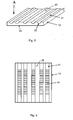
- Fig. 1 shows a one-piece support device 1 with a plurality of slots 4. These are perpendicular to the cutting plane S and distributed over the width B of the support device introduced into this and form Spülkanäle 15.
- a first surface 2 an unillustrated block of material is firmly applied, glued in most cases.
- the second surface 3 of the carrier device 1 is connected to a machine holder, for. B. also glued to this machine holder and clamped in the cutting device.
- the carrier device 1 can also be clamped directly into the cutting machine, depending on the material from which it is made.
- One or more cutting wires are attached to the surface 2 opposite surface of the block of material.
- a cutting aid for example, silicon carbide (SiC) is added.
- As a cooling and separating agent z. As a cooling and separating agent z. As polyethylene glycol (PEG) or oil used. The z. B. about 100 .mu.m to 300 .mu.m thick saw wires or saw blades are moved through the block of material in the direction of the carrier device 1.
- PEG polyethylene glycol
- this cutting into the carrier device 1 is utilized in order to introduce flushing openings into the oblong holes 4 or flushing channels 15.
- the sawn material block is rinsed with a rinsing medium to remove the existing grinding dust and other aids from the shegeschlitzen and separate the wafers from each other.
- tubular scavenging fingers are introduced into the oblong holes 4, which release a flushing medium over the entire length of the oblong holes 4.
- the flushing medium is passed through the resulting flushing openings in the SAgeschlitze between the wafers or sprayed under pressure and rinses the Sgeschlitz and the surface of the wafer free.
- Fig. 2 shows a two-part support device 10 to which a block of material 13 is attached.
- the material block 13 is bonded to a first carrier element 12 with an adhesive which is introduced into an adhesive joint 16.
- a second support member 11 which consists for example of stainless steel, is also connected to the first support member, for. B. by adhesive such as two-component adhesive, which is introduced into a further adhesive groove 16 between the first and second support member, free of movement.
- elongated holes 4 serving as flushing passages 15 are formed perpendicular to the cutting direction S in the support device 10.
- a profile is formed in each case in one surface of the two carrier elements 11, 12.
- This profile consists of a plurality of grooves which are aligned approximately perpendicular to the cutting plane S of the material block 13. The grooves are distributed at the same or different distances from each other over the width B of the two support elements 11, 12.
- the two carrier elements 11, 12 each have a counter-shaped profile and are connected to each other at this profiled surface.
- the first support member 12 made of glass, in particular soda-lime glass, with a thickness 18 between 7 mm and 15 mm, most preferably 12 mm.
- the second carrier element 11 is preferably made of a metallic material, for. B. stainless steel or brass and has a thickness 17 of z. B. 10 to 25 mm, preferably from 12 to 20 mm.
- the width 19 of a flushing channel 15 is preferably 10 to 15 mm, in particular 12 mm.
- the saw wire or the cutting blade is not only passed through the material block 13, but cuts into the first support member, so that the resulting saw slots 14 extend to the profiled surface 20 of the first support member 12.
- scavenging fingers are introduced into the scavenging passages 15, which emit scavenging medium.
- the rinsing medium is discharged through the resulting rinsing openings in the resulting SAgellitze 14 between the wafers.
- the wafers are detached from the carrier device 10 after cutting.
- the first and the second carrier element are separated from each other.
- the first carrier element 12 is supplied for disposal, the second carrier element 11 is reused. For cutting a further block of material, only a new first carrier element 12 is connected to the second carrier element 11.
- Fig. 3 shows a first carrier element 12. It has a non-profiled surface 23, which is connected to the block of material, not shown. This non-profiled surface 23 is opposite a profiled surface 20, are introduced into the grooves 21 perpendicular to the sawing plane S. These grooves are usually introduced by milling or in a surface grinding process. In the Fig. 3 shown grooves have a round groove contour 22. Other contour shapes 22, z. B. angular, are also possible and can be adapted to the purge system used, in particular to the shape of the purge finger used.
- Fig. 4 shows a plan view of the in Fig. 3
- the profiled surface 20 has slot-shaped flushing openings 24 in the grooves 21, the width of which along the groove corresponds to the thickness of the sawing wire or the cutting blade equivalent.
- the width of a flushing opening 24 is determined by the incision depth and the contour of the groove. By a round groove contour and different incision depth, the width of the flushing opening can be varied, with a quadrangular groove contour, the width of the flushing opening remains constant at each incision depth. By an appropriate choice of the groove contour thus different Spülö Stammsstellen can be adjusted.
Description
Die Erfindung betrifft eine Trägervorrichtung zur Befestigung eines Materialblocks in einer Schneidevorrichtung beim Schneiden von Wafern gemäß dem Oberbegriff des Anspruchs 1 sowie ein Verfahren zum Schneiden und Trennen von Wafern aus einem mit der Trägervorrichtung verbundenen Materialblocks gemäß dem Oberbegriff des Anspruchs 12 Eine solche Trägervorrichtung und ein solches Verfahren sind der
Zur Herstellung insbesondere von Solarzellen werden sehr dünne Scheiben, sogenannte Wafer, aus einem Materialblock aus kristallinem Silizium geschnitten. Der Silizium-Materialblock wird als Silizium-Ingot bezeichnet und liegt meist in Quader- oder Zylinderform vor. Ein Silizium-Ingot wird durch Sägen insbesondere mittels einer Drahtsäge zu einzelnen Wafern zerteilt. Typische Draht- bzw. Sägeblattdicken liegen bei 100 bis 300 µm. Aus einem Quader mit 125mm Seitenlänge entstehen somit ca. 175 bis 400 Wafer einer Stärke von 200 bis 400 µm. Um ein Anhaften der einzelnen Wafer untereinander nach dem Sägeschritt zu verhindern, wird der gesägte Materialblock mit einem Spülmedium gespült um das noch vorhandene Slurry aus dem Sägeschlitzen zu entfernen.For the production of solar cells in particular very thin slices, so-called wafers, cut from a block of material of crystalline silicon. The silicon material block is referred to as silicon ingot and is usually in cuboid or cylindrical shape. A silicon ingot is cut into individual wafers by sawing, in particular by means of a wire saw. Typical wire or saw blade thicknesses are 100 to 300 μm. From a parallelepiped with 125mm side length thus arise about 175 to 400 wafers of a thickness of 200 to 400 microns. In order to prevent adhesion of the individual wafers to one another after the sawing step, the sawn material block is rinsed with a rinsing medium in order to remove the remaining slurry from the sawing slits.
Die
Das in der
Aus der
Es ist somit die Aufgabe der vorliegenden Erfindung eine Trägervorrichtung zur Befestigung eines Materialblocks beim Schneiden zu Wafer sowie ein Verfahren zum Schneiden von Wafern zu beschreiben, bei dem die Wafer vollständig und mit geringer mechanischer Belastung voneinander getrennt werden können. Die entsprechende Vorrichtung und das Verfahren sollen dabei möglichst kostengünstig und einfach herstell- bzw. durchführbar sein.It is therefore the object of the present invention to describe a carrier device for fixing a material block when cutting into wafers and a method for cutting wafers, in which the wafers can be completely separated from each other with little mechanical stress. The corresponding device and the method should be as cost-effective and easy to manufacture or feasible.
Die Aufgabe wird durch die erfindungsgemäße Trägervorrichtung gemäß Anspruch 1 sowie dem erfindungsgemäßen Verfahren entsprechend Anspruch 12 gelöst. In den Unteransprüchen sind vorteilhafte Weiterbildungen der erfindungsgemäßen Trägervorrichtung und des Verfahrens dargestellt.The object is achieved by the carrier device according to the invention according to claim 1 and the method according to the invention according to
Die erfindungsgemäße Trägervorrichtung zur Befestigung eines Materialblocks in einer Schneidevorrichtung beim Schneiden zu Wafern wird der Materialblock auf einer Oberfläche der Trägervorrichtung verrutschsicher fixiert, wobei eine Mehrzahl von Langlöchern senkrecht zur Schneideebene der Schneidevorrichtung und verteilt über die Breite der Trägervorrichtung in die Trägervorrichtung eingebracht sind und Spülkanäle bilden.The carrier device according to the invention for fixing a block of material in a cutting device in Cutting into wafers, the block of material is fixed against slipping on a surface of the carrier device, wherein a plurality of oblong holes perpendicular to the cutting plane of the cutting device and distributed over the width of the carrier device are introduced into the carrier device and form flushing channels.
Durch das Einschneiden der Schneidevorrichtung in die Langlöcher sind bevorzugt Spülöffnungen ausgebildet.By cutting the cutting device in the slots preferably scavenging holes are formed.
Durch diese Spülkanäle kann das Spülmedium über die Spülöffnungen verteilt über die gesamte Breite der Wafer, in die Sägeschlitze eingebracht werden. Somit kann eine gleichmäßige Verteilung von Spülmedium über die gesamte Breite des Wafers sowie in alle Sägeschlitze des Materialblocks sichergestellt werden. Das Spülmedium muss lediglich mit geringem Druck über die Spülöffnungen eingebracht werden und reduziert somit die mechanische Belastung der einzelnen Wafer und ihrer Oberflächen.Through these flushing channels, the flushing medium distributed over the flushing openings can be introduced over the entire width of the wafer in the Sägeschlitze. Thus, a uniform distribution of flushing medium over the entire width of the wafer and in all Sägeschlitze the block of material can be ensured. The flushing medium only has to be introduced at low pressure via the flushing openings and thus reduces the mechanical load on the individual wafers and their surfaces.
Erfindungsgemäß besteht die Trägervorrichtung aus mindestens zwei Trägerelementen.According to the invention, the carrier device consists of at least two carrier elements.
Der Aufbau der Trägervorrichtung aus mindestens zwei Trägerelementen hat den Vorteil, dass die Trägerelemente nach dem Schneiden des Materialblocks zu Wafern wieder voneinander getrennt werden können und das oder die Trägerelemente, die nicht eingesägt sind, für das Schneiden eines weiteren Materialblocks verwendet werden können. Ein Großteil der Trägervorrichtung kann somit wiederverwendet und somit kann die Herstellungskosten der Wafer reduziert werden.The construction of the carrier device comprising at least two carrier elements has the advantage that after the material block has been cut into wafers, the carrier elements can be separated from one another again and the carrier element or elements which are not sawed in can be used for cutting a further material block. A large part of the carrier device can thus reused, and thus the manufacturing cost of the wafer can be reduced.
Vorteilhafterweise besteht das erste Trägerelement aus Glas, insbesondere aus Kalk-Natron-Glas. Dieses wird als Flachglas gefertigt, wobei das Profil in einfacher weise durch Fräsen, Schleifen, Lasern und/oder Bohren eingebracht ist. Das erste Trägerelement ist somit in großer Stückzahl kostengünstig herstellbar und jederzeit verfügbar. Dies erlaubt eine geringe Lagerhaltung und dementsprechend wenig Kosten.Advantageously, the first carrier element made of glass, in particular soda-lime glass. This is made as a flat glass, the profile is introduced in a simple manner by milling, grinding, lasers and / or drilling. The first carrier element is thus inexpensive to produce in large quantities and available at any time. This allows a low storage and therefore little cost.
Es ist ebenfalls vorteilhaft, dass die mindestens zwei Trägerelemente durch Kleben miteinander verbunden sind. Durch den Einsatz von entsprechenden Lösungsmitteln können nicht nur die Wafer vom ersten Trägerelement getrennt, sondern gleichzeitig die Trägerelemente voneinander gelöst werden.It is also advantageous that the at least two carrier elements are connected to one another by gluing. By using appropriate solvents, not only the wafers can be separated from the first carrier element, but at the same time the carrier elements can be detached from one another.
Die Aufgabe wird ebenfalls in vorteilhafter Weise durch das erfindungsgemäße Verfahren gelöst. Dabei ist ein Materialblock auf einer erfindungsgemäßen Trägervorrichtung befestigt und wird in einer Schneidevorrichtung geschnitten. Dabei schneidet die Schneidevorrichtung bis in die Spülkanäle der Trägervorrichtung ein und erzeugt dabei Spülöffnungen. Danach wird Spülmedium in die Spülkanäle der Trägervorrichtung eingebracht, das durch die Spülöffnungen zu den Wafern geführt wird.The object is likewise achieved in an advantageous manner by the method according to the invention. In this case, a block of material is mounted on a carrier device according to the invention and is cut in a cutting device. In this case, the cutting device cuts into the flushing channels of the support device and thereby generates flushing openings. Thereafter, flushing medium is introduced into the flushing channels of the support device, which is guided through the flushing openings to the wafers.
Dieses Verfahren erlaubt eine einfache Spülung der Sägeschlitze zwischen den einzelnen Wafern über die gesamte Breite der Wafer hinweg. Da die Spülöffnungen durch das Einschneiden der Schneidevorrichtung in die Trägervorrichtung erzeugt werden, sind die Spülöffnungen jeweils genau in den Spalten zwischen den Wafern platziert. Somit kann bei unterschiedlich dicken Wafern immer die gleiche Trägervorrichtung verwendet werden. Es wird somit lediglich eine Trägervorrichtung benötigt, die in einer großen Stückzahl günstig hergestellt bzw. in großer Stückzahl erworben werden.This method allows for easy rinsing of the saw slots between the individual wafers across the entire width of the wafer. Since the scavenging ports are formed by cutting the cutter into the carrier device, the scavenging ports are respectively placed exactly in the gaps between the wafers. Thus, with different thickness wafers always the same support device can be used. It Therefore, only one carrier device is needed, which are produced inexpensively in a large number or purchased in large quantities.
Da die Spülkanäle in ihrer Längsausdehnung vollständig von der Trägervorrichtung umschlossen und vor dem Schneiden keine Spülöffnungen vorhanden sind, können die Spülkanäle beim Befestigen des Materialblocks an der Trägervorrichtung nicht, z.B. durch Klebemittel, verunreinigt werden. Somit ist eine zuverlässige Verteilung von Spülmittel über die gesamte Länge des Spülkanals sichergestellt.Since the purge channels are completely enclosed by the carrier device in their longitudinal extent and no scavenging ports are present prior to cutting, the scavenging passages can not be fixed, for example when attaching the block of material to the carrier device. by adhesive, be contaminated. Thus, a reliable distribution of detergent over the entire length of the flushing channel is ensured.
Ausführungsbeispiele der erfindungsgemäßen Trägervorrichtung sowie des Verfahrens zum Schneiden und Ablösen von Wafern aus einem Materialblock sind in der Zeichnung beispielhaft dargestellt und werden anhand der folgenden Beschreibung näher erläutert. Es zeigen:
- Fig. 1
- ein Beispiel einer nicht erfindungsgemäßen Trägervorrichtung in perspektivischer Ansicht;
- Fig. 2
- ein Ausführungsbeispiel einer erfindungsgemäßes Trägervorrichtung verbunden mit einem Materialblock in perspektivischer Ansicht;
- Fig. 3
- ein Ausführungsbeispiel eines erfindungsgemäßen ersten Trägerelementes in perspektivischer Ansicht und
- Fig. 4
- eine Draufsicht auf die profilierte Oberfläche des in
Fig. 3 gezeigten ersten Trägerelements.
- Fig. 1
- an example of a non-inventive carrier device in perspective view;
- Fig. 2
- an embodiment of an inventive carrier device connected to a block of material in perspective view;
- Fig. 3
- An embodiment of a first carrier element according to the invention in a perspective view and
- Fig. 4
- a plan view of the profiled surface of in
Fig. 3 shown first carrier element.
Einander entsprechende Teile sind in allen Figuren mit den gleichen Bezugszeichen versehen.Corresponding parts are provided in all figures with the same reference numerals.
Um sicherzustellen, dass der Materialblock komplett durchschnitten ist, schneidet man üblicherweise in die Trägervorrichtung 1 hinein. In der vorliegenden Erfindung wird dieses Einschneiden in die Trägervorrichtung 1 ausgenutzt, um Spülöffnungen in die Langlöcher 4 bzw. Spülkanäle 15 einzubringen. Nach dem Schneiden wird der gesägte Materialblock mit einem Spülmedium gespült, um den vorhandenen Schleifstaub und die sonstigen Hilfsmittel aus den Sägeschlitzen zu entfernen und die Wafer voneinander zu trennen. Dazu werden röhrenförmige Spülfinger in die Langlöcher 4 eingebracht, die ein Spülmedium über die gesamte Länge der Langlöcher 4 hinweg abgeben. Das Spülmedium wird durch die entstandenen Spülöffnungen in die Sägeschlitze zwischen den Wafern weitergegeben bzw. unter Druck eingesprüht und spült den Sägeschlitz sowie die Oberfläche der Wafer frei.To ensure that the block of material is completely cut through, it is customary to cut into the carrier device 1. In the present invention, this cutting into the carrier device 1 is utilized in order to introduce flushing openings into the oblong holes 4 or flushing channels 15. After cutting, the sawn material block is rinsed with a rinsing medium to remove the existing grinding dust and other aids from the Sägeschlitzen and separate the wafers from each other. For this purpose, tubular scavenging fingers are introduced into the oblong holes 4, which release a flushing medium over the entire length of the oblong holes 4. The flushing medium is passed through the resulting flushing openings in the Sägeschlitze between the wafers or sprayed under pressure and rinses the Sägeschlitz and the surface of the wafer free.
Wie im Fall der einteiligen Trägervorrichtung 1, sind auch in der zweiteiligen Trägervorrichtung 10 Langlöcher 4, die als Spülkanäle 15 dienen, senkrecht zur Schneiderichtung S in der Trägervorrichtung 10 ausgebildet. Dazu ist in jeweils einer Oberfläche der beiden Trägerelemente 11, 12 ein Profil ausgeformt. Dieses Profil besteht aus einer Mehrzahl von Nuten, die in etwa senkrecht zur Schneideebene S des Materialblocks 13 ausgerichtet sind. Die Nuten sind mit gleichem oder auch unterschiedlichem Abstand voneinander über die Breite B der beiden Trägerelemente 11, 12 verteilt. Die zwei Trägerelemente 11, 12 weisen ein jeweils gegengleich ausgeformtes Profil auf und sind an diesen profilierten Oberfläche miteinander verbunden.As in the case of the one-piece support device 1, also in the two-
Bevorzugterweise besteht das erste Trägerelement 12 aus Glas, insbesondere aus Kalk-Natron-Glas, mit einer Stärke 18 zwischen 7 mm und 15 mm, in besonders bevorzugter Weise von 12 mm. Das zweite Trägerelement 11 ist bevorzugterweise aus einem metallischen Material, z. B. rostfreiem Stahl oder Messing gefertigt und weist eine Stärke 17 von z. B. 10 bis 25 mm, bevorzugt von 12 bis 20 mm auf. Die Weite 19 eines Spülkanals 15 beträgt vorzugsweise 10 bis 15 mm, insbesondere 12 mm.Preferably, the
Beim Schneiden der Wafer wird der Sägedraht bzw. das Schneidblatt nicht nur durch den Materialblock 13 hindurchgeführt, sondern schneidet in das erste Trägerelement ein, so dass die entstandenen Sägeschlitze 14 bis an die profilierte Oberfläche 20 des ersten Trägerelements 12 hineinreichen. Wie bei der einteiligen Trägervorrichtung 1 werden Spülfinger in die Spülkanäle 15 eingeführt, die Spülmedium abgeben. Das Spülmedium wird über die entstandenen Spülöffnungen in die entstandenen Sägeschlitze 14 zwischen den Wafern abgegeben. Die Wafer werden nach dem Schneiden von der Trägervorrichtung 10 abgelöst. Ebenso werden das erste und das zweite Trägerelement voneinander getrennt. Das erste Trägerelement 12 wird der Entsorgung zugeführt, das zweite Trägerelement 11 wird wiederverwendet. Zum Schneiden eines weiteren Materialblocks wird lediglich ein neues erstes Trägerelement 12 mit dem zweiten Trägerelement 11 verbunden.When cutting the wafer, the saw wire or the cutting blade is not only passed through the
Alle beschriebenen und/oder bezeichneten Merkmale können im Rahmen der Erfindung vorteilhaft miteinander kombiniert werden. Die Erfindung ist nicht auf die Ausführungsbeispiele beschränkt.All described and / or designated features can be combined advantageously within the scope of the invention. The invention is not limited to the embodiments.
Claims (13)
- Carrier device for fastening a material block (13) in a cutting device while it is being cut into wafers, wherein the carrier device is configured such that the material block (13) is fixable in a non-slip manner on a surface (2) of the carrier device and the passage direction of through-slots (4) is oriented perpendicularly to the plane of introduced saw cuts (14) and such that the slots (4) are introduced into the carrier device (1, 10) across the width (B) and form rinsing ducts (15), wherein the carrier device (1, 10) consists of at least two carrier elements (11, 12),
characterized
in that two carrier elements (11, 12) each have a surface (20) that is profiled in a mirror-inverted manner, and the two carrier elements (11, 12) are connected together at the respectively profiled surfaces (20) and form the rinsing ducts (15). - Carrier device according to Claim 1,
characterized
in that the first carrier element (12) consists of an amorphous material. - Carrier device according to Claim 1,
characterized
in that the first carrier element (12) consists of glass, in particular of soda-lime glass. - Carrier device according to Claim 1,
characterized
in that the second carrier element (11) consists of an inorganic material, preferably of a metal material. - Carrier device according to Claim 1,
characterized
in that the first carrier element (12) is made of glass and the second carrier element (11) is made of a metal material. - Carrier device according to Claim 1 and 5,
characterized
in that rinsing openings (24) are formed by the saw cuts (14) in the slots (4). - Carrier device according to one of Claims 1 to 6,
characterized
in that in each case at least one surface (20) of a carrier element (11, 12) has an uneven profile. - Carrier device according to one of Claims 1 to 7,
characterized
in that the profile of one carrier element (11, 12) consists of a plurality of grooves (21) which are oriented approximately perpendicularly to the plane of the introduced saw cuts (14). - Carrier device according to one of Claims 1 to 8,
characterized
in that the profile of the first carrier element (12) is introduced by milling, grinding, laser-cutting and/or drilling. - Carrier device according to one of Claims 1 to 9,
characterized
in that the second carrier element (11) is connectable to the cutting device. - Carrier device according to one of Claims 1 to 10,
characterized
in that the two carrier elements (11, 12) are connected together by adhesive bonding. - Method for cutting and detaching wafers from a material block (13),
wherein the material block (13) is fastened to a carrier device (1, 10) which is configured such that the material block (13) is fixable in a non-slip manner on a surface (2) of the carrier device and through-slots (4) are introduced into the carrier device (1, 10) in a manner distributed across the width (B) and form rinsing ducts (15), wherein the carrier device (1, 10) consists of at least two carrier elements (11, 12), wherein the material block is fixed to a first carrier element (12), wherein the material block (13) is cut in a cutting device, wherein the cutting device cuts into rinsing ducts (15) of the carrier device (1, 10) and creates rinsing openings (24), and
wherein rinsing medium is introduced into the rinsing ducts (15) of the carrier device (1, 10), said rinsing medium being guided through the rinsing openings (24) to the wafers
characterized
in that the two carrier elements (11, 12) each have a surface (20) that is profiled in a mirror-inverted manner, wherein the two carrier elements (11, 12) are connected together at the respectively profiled surfaces (20) and form the rinsing ducts (15), and
in that the cutting device cuts into the profiled surface (20) of the first carrier element (12). - Method according to Claim 12,
characterized
in that, after cutting, the first carrier element (12) is detached from the carrier device (10) and is replaced by an unused other carrier element.
Applications Claiming Priority (4)
| Application Number | Priority Date | Filing Date | Title |
|---|---|---|---|
| DE102010026631 | 2010-07-09 | ||
| DE102010034945 | 2010-08-20 | ||
| DE102010050897.7A DE102010050897B4 (en) | 2010-07-09 | 2010-11-10 | Carrier device and method for cutting a block of material attached to the carrier device |
| PCT/EP2011/058719 WO2012004052A1 (en) | 2010-07-09 | 2011-05-27 | Carrier device and method for cutting a material block fixed to the carrier device |
Publications (2)
| Publication Number | Publication Date |
|---|---|
| EP2590789A1 EP2590789A1 (en) | 2013-05-15 |
| EP2590789B1 true EP2590789B1 (en) | 2015-07-01 |
Family
ID=45372691
Family Applications (1)
| Application Number | Title | Priority Date | Filing Date |
|---|---|---|---|
| EP11721555.8A Active EP2590789B1 (en) | 2010-07-09 | 2011-05-27 | Carrier device and method for cutting a material block fixed to the carrier device |
Country Status (5)
| Country | Link |
|---|---|
| EP (1) | EP2590789B1 (en) |
| KR (1) | KR101762998B1 (en) |
| DE (1) | DE102010050897B4 (en) |
| TW (1) | TWI589419B (en) |
| WO (1) | WO2012004052A1 (en) |
Families Citing this family (5)
| Publication number | Priority date | Publication date | Assignee | Title |
|---|---|---|---|---|
| DE102010031364A1 (en) * | 2010-07-15 | 2012-01-19 | Gebr. Schmid Gmbh & Co. | Support for a silicon block, carrier arrangement with such a carrier and method for producing such a carrier arrangement |
| DE102010052635B4 (en) * | 2010-11-29 | 2014-01-02 | Rena Gmbh | Holding cleaning device and method for sectionally cleaning sawn wafers |
| EP2711151A1 (en) | 2012-09-24 | 2014-03-26 | Meyer Burger AG | Method of making wafers |
| CN107856210B (en) * | 2017-11-23 | 2018-08-21 | 江苏高照新能源发展有限公司 | Silicon wafer cut by diamond wire resin plate and degumming process method |
| DE102021109459A1 (en) * | 2021-04-15 | 2022-10-20 | Fraunhofer-Gesellschaft zur Förderung der angewandten Forschung eingetragener Verein | Process for fixing a block of material for mechanical processing |
Family Cites Families (9)
| Publication number | Priority date | Publication date | Assignee | Title |
|---|---|---|---|---|
| JPH09207126A (en) * | 1996-01-31 | 1997-08-12 | Nippei Toyama Corp | Work supporting apparatus for wire saw, method for cleaning in and the wire saw |
| DE19900671C2 (en) * | 1999-01-11 | 2002-04-25 | Fraunhofer Ges Forschung | Method and device for separating disk-shaped substrates, in particular for wafer production |
| DE102004058194A1 (en) * | 2004-12-02 | 2005-08-11 | Siltronic Ag | Saw-strip, has two surfaces fixed to crystal piece and carrier plate, respectively, where strip cuts semi conductor disc from piece using wire saw and separates from strip by drilling holes in strip |
| DE102004058195A1 (en) | 2004-12-02 | 2006-06-08 | Patent-Treuhand-Gesellschaft für elektrische Glühlampen mbH | Conductor holder |
| DE102005028112A1 (en) * | 2005-06-13 | 2006-12-21 | Schmid Technology Systems Gmbh | Method for positioning and maintaining the position of substrates, in particular of thin silicon wafers after wire sawing for their separation |
| EP2111960B1 (en) * | 2008-04-23 | 2011-03-09 | Applied Materials Switzerland SA | Mounting plate for a wire sawing device, wire sawing device comprising the same, and wire sawing process carried out by the device |
| DE102008037652A1 (en) * | 2008-08-14 | 2010-04-29 | Wacker Schott Solar Gmbh | Carrier, method and apparatus for producing wafers and use of the produced wafers |
| DE102008045990A1 (en) | 2008-09-05 | 2010-03-11 | Wacker Schott Solar Gmbh | Device for processing wafer comb made up of wafer, has supplying unit for supplying rinsing fluid to wafer comb, where supplying unit has slot nozzle |
| DE102009023121A1 (en) * | 2009-05-22 | 2010-11-25 | Gebr. Schmid Gmbh & Co. | Support for a silicon block |
-
2010
- 2010-11-10 DE DE102010050897.7A patent/DE102010050897B4/en active Active
-
2011
- 2011-05-27 WO PCT/EP2011/058719 patent/WO2012004052A1/en active Application Filing
- 2011-05-27 EP EP11721555.8A patent/EP2590789B1/en active Active
- 2011-05-27 KR KR1020137000514A patent/KR101762998B1/en active IP Right Grant
- 2011-06-09 TW TW100120101A patent/TWI589419B/en active
Also Published As
| Publication number | Publication date |
|---|---|
| EP2590789A1 (en) | 2013-05-15 |
| TWI589419B (en) | 2017-07-01 |
| KR20130088123A (en) | 2013-08-07 |
| DE102010050897A1 (en) | 2012-01-12 |
| KR101762998B1 (en) | 2017-07-28 |
| DE102010050897B4 (en) | 2014-05-22 |
| WO2012004052A1 (en) | 2012-01-12 |
| TW201204523A (en) | 2012-02-01 |
Similar Documents
| Publication | Publication Date | Title |
|---|---|---|
| EP1901897B1 (en) | Device for positioning and blocking thin substrates on a cut substrate block | |
| EP2590789B1 (en) | Carrier device and method for cutting a material block fixed to the carrier device | |
| DE102006050330B4 (en) | A method for simultaneously separating at least two cylindrical workpieces into a plurality of slices | |
| DE102010052635B4 (en) | Holding cleaning device and method for sectionally cleaning sawn wafers | |
| EP2298520A1 (en) | Method and device for cleaning wafers | |
| EP0185355A1 (en) | Method of manufacturing blade stacks for dividing crystal bars into wafers | |
| DE102016111543A1 (en) | Saw blade for a circular saw, method of making a saw blade and circular saw | |
| WO2012007381A1 (en) | Carrier for a silicon block, carrier arrangement having such a carrier and process for producing such a carrier arrangement | |
| EP2765617A2 (en) | Method for producing wafers, in particular wafers for solar cells, and device for producing wafers | |
| EP1741517B1 (en) | Vacuum clamping device for fixing a sheet and method for machining the sheet | |
| DE102008037653B4 (en) | Process for the production of wafers and block holders | |
| EP0366056B1 (en) | Internal diameter saw blade | |
| WO2014111304A1 (en) | Clampable cementing strip for a wire sawing process | |
| DE2530569C3 (en) | Carriers with glued-on blocks of material and manufacturing processes therefor | |
| DE102007004778B3 (en) | Method for producing piezo bending converter, involves supplying multilevel plate like piezo utility with multiple slat like lamella output structures, where openings in direction of thickness by piezo utility | |
| DE102021104322A1 (en) | Method of attaching multiple knife holders to a slitter, assembly kit for attaching multiple knife holders to a slitter, knife holder, positioning bar, and slitter | |
| EP4323167A1 (en) | Method for fixing a material block for mechanical machining | |
| DE102009060575B9 (en) | Method and device for separating wafers from an ingot | |
| DE102006053943A1 (en) | Guide for recirculating bandsaw blade dividing silicon monocrystals to make wafers used in electronics industry, is grooved, water-cushioned, and replaceably dovetail-mounted | |
| WO2013023799A1 (en) | Method for conditioning flat objects | |
| DE10008409A1 (en) | Tensioning system for frame saws has flexible traction elements connected to one end of saw blades and passing over deflector elements | |
| DE102009045614A1 (en) | Method for cutting e.g. workpiece block from e.g. silicon, involves laterally forming rectangular groove with depth on rear side of workpiece and offset to separation line formed perpendicular to front side of workpiece | |
| EP3293313A1 (en) | Cutting tool | |
| DE102016222899A1 (en) | Apparatus and method for sawing a workpiece with a wire saw | |
| DE19905751A1 (en) | Inner hole saw and method for adjusting a nozzle and a sensor of an inner hole saw relative to a saw blade of the inner hole saw |
Legal Events
| Date | Code | Title | Description |
|---|---|---|---|
| PUAI | Public reference made under article 153(3) epc to a published international application that has entered the european phase |
Free format text: ORIGINAL CODE: 0009012 |
|
| 17P | Request for examination filed |
Effective date: 20121112 |
|
| AK | Designated contracting states |
Kind code of ref document: A1 Designated state(s): AL AT BE BG CH CY CZ DE DK EE ES FI FR GB GR HR HU IE IS IT LI LT LU LV MC MK MT NL NO PL PT RO RS SE SI SK SM TR |
|
| DAX | Request for extension of the european patent (deleted) | ||
| GRAP | Despatch of communication of intention to grant a patent |
Free format text: ORIGINAL CODE: EPIDOSNIGR1 |
|
| INTG | Intention to grant announced |
Effective date: 20150129 |
|
| GRAS | Grant fee paid |
Free format text: ORIGINAL CODE: EPIDOSNIGR3 |
|
| GRAA | (expected) grant |
Free format text: ORIGINAL CODE: 0009210 |
|
| AK | Designated contracting states |
Kind code of ref document: B1 Designated state(s): AL AT BE BG CH CY CZ DE DK EE ES FI FR GB GR HR HU IE IS IT LI LT LU LV MC MK MT NL NO PL PT RO RS SE SI SK SM TR |
|
| REG | Reference to a national code |
Ref country code: GB Ref legal event code: FG4D Free format text: NOT ENGLISH |
|
| REG | Reference to a national code |
Ref country code: AT Ref legal event code: REF Ref document number: 733678 Country of ref document: AT Kind code of ref document: T Effective date: 20150715 Ref country code: CH Ref legal event code: EP |
|
| REG | Reference to a national code |
Ref country code: IE Ref legal event code: FG4D Free format text: LANGUAGE OF EP DOCUMENT: GERMAN |
|
| REG | Reference to a national code |
Ref country code: DE Ref legal event code: R096 Ref document number: 502011007203 Country of ref document: DE |
|
| REG | Reference to a national code |
Ref country code: NL Ref legal event code: MP Effective date: 20150701 |
|
| REG | Reference to a national code |
Ref country code: LT Ref legal event code: MG4D |
|
| PG25 | Lapsed in a contracting state [announced via postgrant information from national office to epo] |
Ref country code: GR Free format text: LAPSE BECAUSE OF FAILURE TO SUBMIT A TRANSLATION OF THE DESCRIPTION OR TO PAY THE FEE WITHIN THE PRESCRIBED TIME-LIMIT Effective date: 20151002 Ref country code: LV Free format text: LAPSE BECAUSE OF FAILURE TO SUBMIT A TRANSLATION OF THE DESCRIPTION OR TO PAY THE FEE WITHIN THE PRESCRIBED TIME-LIMIT Effective date: 20150701 Ref country code: NO Free format text: LAPSE BECAUSE OF FAILURE TO SUBMIT A TRANSLATION OF THE DESCRIPTION OR TO PAY THE FEE WITHIN THE PRESCRIBED TIME-LIMIT Effective date: 20151001 Ref country code: LT Free format text: LAPSE BECAUSE OF FAILURE TO SUBMIT A TRANSLATION OF THE DESCRIPTION OR TO PAY THE FEE WITHIN THE PRESCRIBED TIME-LIMIT Effective date: 20150701 Ref country code: FI Free format text: LAPSE BECAUSE OF FAILURE TO SUBMIT A TRANSLATION OF THE DESCRIPTION OR TO PAY THE FEE WITHIN THE PRESCRIBED TIME-LIMIT Effective date: 20150701 |
|
| PG25 | Lapsed in a contracting state [announced via postgrant information from national office to epo] |
Ref country code: IS Free format text: LAPSE BECAUSE OF FAILURE TO SUBMIT A TRANSLATION OF THE DESCRIPTION OR TO PAY THE FEE WITHIN THE PRESCRIBED TIME-LIMIT Effective date: 20151101 Ref country code: PL Free format text: LAPSE BECAUSE OF FAILURE TO SUBMIT A TRANSLATION OF THE DESCRIPTION OR TO PAY THE FEE WITHIN THE PRESCRIBED TIME-LIMIT Effective date: 20150701 Ref country code: SE Free format text: LAPSE BECAUSE OF FAILURE TO SUBMIT A TRANSLATION OF THE DESCRIPTION OR TO PAY THE FEE WITHIN THE PRESCRIBED TIME-LIMIT Effective date: 20150701 Ref country code: HR Free format text: LAPSE BECAUSE OF FAILURE TO SUBMIT A TRANSLATION OF THE DESCRIPTION OR TO PAY THE FEE WITHIN THE PRESCRIBED TIME-LIMIT Effective date: 20150701 Ref country code: ES Free format text: LAPSE BECAUSE OF FAILURE TO SUBMIT A TRANSLATION OF THE DESCRIPTION OR TO PAY THE FEE WITHIN THE PRESCRIBED TIME-LIMIT Effective date: 20150701 Ref country code: PT Free format text: LAPSE BECAUSE OF FAILURE TO SUBMIT A TRANSLATION OF THE DESCRIPTION OR TO PAY THE FEE WITHIN THE PRESCRIBED TIME-LIMIT Effective date: 20151102 Ref country code: RS Free format text: LAPSE BECAUSE OF FAILURE TO SUBMIT A TRANSLATION OF THE DESCRIPTION OR TO PAY THE FEE WITHIN THE PRESCRIBED TIME-LIMIT Effective date: 20150701 |
|
| REG | Reference to a national code |
Ref country code: DE Ref legal event code: R097 Ref document number: 502011007203 Country of ref document: DE |
|
| PG25 | Lapsed in a contracting state [announced via postgrant information from national office to epo] |
Ref country code: EE Free format text: LAPSE BECAUSE OF FAILURE TO SUBMIT A TRANSLATION OF THE DESCRIPTION OR TO PAY THE FEE WITHIN THE PRESCRIBED TIME-LIMIT Effective date: 20150701 Ref country code: IT Free format text: LAPSE BECAUSE OF FAILURE TO SUBMIT A TRANSLATION OF THE DESCRIPTION OR TO PAY THE FEE WITHIN THE PRESCRIBED TIME-LIMIT Effective date: 20150701 Ref country code: SK Free format text: LAPSE BECAUSE OF FAILURE TO SUBMIT A TRANSLATION OF THE DESCRIPTION OR TO PAY THE FEE WITHIN THE PRESCRIBED TIME-LIMIT Effective date: 20150701 Ref country code: DK Free format text: LAPSE BECAUSE OF FAILURE TO SUBMIT A TRANSLATION OF THE DESCRIPTION OR TO PAY THE FEE WITHIN THE PRESCRIBED TIME-LIMIT Effective date: 20150701 Ref country code: CZ Free format text: LAPSE BECAUSE OF FAILURE TO SUBMIT A TRANSLATION OF THE DESCRIPTION OR TO PAY THE FEE WITHIN THE PRESCRIBED TIME-LIMIT Effective date: 20150701 |
|
| PLBE | No opposition filed within time limit |
Free format text: ORIGINAL CODE: 0009261 |
|
| STAA | Information on the status of an ep patent application or granted ep patent |
Free format text: STATUS: NO OPPOSITION FILED WITHIN TIME LIMIT |
|
| REG | Reference to a national code |
Ref country code: FR Ref legal event code: PLFP Year of fee payment: 6 |
|
| PG25 | Lapsed in a contracting state [announced via postgrant information from national office to epo] |
Ref country code: RO Free format text: LAPSE BECAUSE OF FAILURE TO SUBMIT A TRANSLATION OF THE DESCRIPTION OR TO PAY THE FEE WITHIN THE PRESCRIBED TIME-LIMIT Effective date: 20150701 |
|
| 26N | No opposition filed |
Effective date: 20160404 |
|
| PG25 | Lapsed in a contracting state [announced via postgrant information from national office to epo] |
Ref country code: SI Free format text: LAPSE BECAUSE OF FAILURE TO SUBMIT A TRANSLATION OF THE DESCRIPTION OR TO PAY THE FEE WITHIN THE PRESCRIBED TIME-LIMIT Effective date: 20150701 Ref country code: BE Free format text: LAPSE BECAUSE OF NON-PAYMENT OF DUE FEES Effective date: 20160531 |
|
| PG25 | Lapsed in a contracting state [announced via postgrant information from national office to epo] |
Ref country code: LU Free format text: LAPSE BECAUSE OF FAILURE TO SUBMIT A TRANSLATION OF THE DESCRIPTION OR TO PAY THE FEE WITHIN THE PRESCRIBED TIME-LIMIT Effective date: 20160527 |
|
| REG | Reference to a national code |
Ref country code: CH Ref legal event code: PL |
|
| PG25 | Lapsed in a contracting state [announced via postgrant information from national office to epo] |
Ref country code: CH Free format text: LAPSE BECAUSE OF NON-PAYMENT OF DUE FEES Effective date: 20160531 Ref country code: LI Free format text: LAPSE BECAUSE OF NON-PAYMENT OF DUE FEES Effective date: 20160531 |
|
| REG | Reference to a national code |
Ref country code: IE Ref legal event code: MM4A |
|
| REG | Reference to a national code |
Ref country code: FR Ref legal event code: PLFP Year of fee payment: 7 |
|
| PG25 | Lapsed in a contracting state [announced via postgrant information from national office to epo] |
Ref country code: IE Free format text: LAPSE BECAUSE OF NON-PAYMENT OF DUE FEES Effective date: 20160527 |
|
| PG25 | Lapsed in a contracting state [announced via postgrant information from national office to epo] |
Ref country code: NL Free format text: LAPSE BECAUSE OF FAILURE TO SUBMIT A TRANSLATION OF THE DESCRIPTION OR TO PAY THE FEE WITHIN THE PRESCRIBED TIME-LIMIT Effective date: 20150701 |
|
| REG | Reference to a national code |
Ref country code: AT Ref legal event code: MM01 Ref document number: 733678 Country of ref document: AT Kind code of ref document: T Effective date: 20160527 |
|
| PG25 | Lapsed in a contracting state [announced via postgrant information from national office to epo] |
Ref country code: AT Free format text: LAPSE BECAUSE OF NON-PAYMENT OF DUE FEES Effective date: 20160527 |
|
| REG | Reference to a national code |
Ref country code: FR Ref legal event code: PLFP Year of fee payment: 8 |
|
| PG25 | Lapsed in a contracting state [announced via postgrant information from national office to epo] |
Ref country code: HU Free format text: LAPSE BECAUSE OF FAILURE TO SUBMIT A TRANSLATION OF THE DESCRIPTION OR TO PAY THE FEE WITHIN THE PRESCRIBED TIME-LIMIT; INVALID AB INITIO Effective date: 20110527 Ref country code: SM Free format text: LAPSE BECAUSE OF FAILURE TO SUBMIT A TRANSLATION OF THE DESCRIPTION OR TO PAY THE FEE WITHIN THE PRESCRIBED TIME-LIMIT Effective date: 20150701 Ref country code: CY Free format text: LAPSE BECAUSE OF FAILURE TO SUBMIT A TRANSLATION OF THE DESCRIPTION OR TO PAY THE FEE WITHIN THE PRESCRIBED TIME-LIMIT Effective date: 20150701 |
|
| PG25 | Lapsed in a contracting state [announced via postgrant information from national office to epo] |
Ref country code: MC Free format text: LAPSE BECAUSE OF FAILURE TO SUBMIT A TRANSLATION OF THE DESCRIPTION OR TO PAY THE FEE WITHIN THE PRESCRIBED TIME-LIMIT Effective date: 20150701 Ref country code: MT Free format text: LAPSE BECAUSE OF FAILURE TO SUBMIT A TRANSLATION OF THE DESCRIPTION OR TO PAY THE FEE WITHIN THE PRESCRIBED TIME-LIMIT Effective date: 20150701 Ref country code: TR Free format text: LAPSE BECAUSE OF FAILURE TO SUBMIT A TRANSLATION OF THE DESCRIPTION OR TO PAY THE FEE WITHIN THE PRESCRIBED TIME-LIMIT Effective date: 20150701 Ref country code: MK Free format text: LAPSE BECAUSE OF FAILURE TO SUBMIT A TRANSLATION OF THE DESCRIPTION OR TO PAY THE FEE WITHIN THE PRESCRIBED TIME-LIMIT Effective date: 20150701 |
|
| PG25 | Lapsed in a contracting state [announced via postgrant information from national office to epo] |
Ref country code: BG Free format text: LAPSE BECAUSE OF FAILURE TO SUBMIT A TRANSLATION OF THE DESCRIPTION OR TO PAY THE FEE WITHIN THE PRESCRIBED TIME-LIMIT Effective date: 20150701 |
|
| PG25 | Lapsed in a contracting state [announced via postgrant information from national office to epo] |
Ref country code: AL Free format text: LAPSE BECAUSE OF FAILURE TO SUBMIT A TRANSLATION OF THE DESCRIPTION OR TO PAY THE FEE WITHIN THE PRESCRIBED TIME-LIMIT Effective date: 20150701 |
|
| PGFP | Annual fee paid to national office [announced via postgrant information from national office to epo] |
Ref country code: FR Payment date: 20230517 Year of fee payment: 13 Ref country code: DE Payment date: 20230424 Year of fee payment: 13 |
|
| PGFP | Annual fee paid to national office [announced via postgrant information from national office to epo] |
Ref country code: GB Payment date: 20230522 Year of fee payment: 13 |