EP2586659A1 - Vehicle headlamp - Google Patents
Vehicle headlamp Download PDFInfo
- Publication number
- EP2586659A1 EP2586659A1 EP12190134.2A EP12190134A EP2586659A1 EP 2586659 A1 EP2586659 A1 EP 2586659A1 EP 12190134 A EP12190134 A EP 12190134A EP 2586659 A1 EP2586659 A1 EP 2586659A1
- Authority
- EP
- European Patent Office
- Prior art keywords
- light emitting
- movable shade
- reflector
- vehicle headlamp
- semiconductor light
- Prior art date
- Legal status (The legal status is an assumption and is not a legal conclusion. Google has not performed a legal analysis and makes no representation as to the accuracy of the status listed.)
- Granted
Links
Images


Classifications
-
- B—PERFORMING OPERATIONS; TRANSPORTING
- B60—VEHICLES IN GENERAL
- B60Q—ARRANGEMENT OF SIGNALLING OR LIGHTING DEVICES, THE MOUNTING OR SUPPORTING THEREOF OR CIRCUITS THEREFOR, FOR VEHICLES IN GENERAL
- B60Q1/00—Arrangement of optical signalling or lighting devices, the mounting or supporting thereof or circuits therefor
- B60Q1/02—Arrangement of optical signalling or lighting devices, the mounting or supporting thereof or circuits therefor the devices being primarily intended to illuminate the way ahead or to illuminate other areas of way or environments
- B60Q1/04—Arrangement of optical signalling or lighting devices, the mounting or supporting thereof or circuits therefor the devices being primarily intended to illuminate the way ahead or to illuminate other areas of way or environments the devices being headlights
- B60Q1/14—Arrangement of optical signalling or lighting devices, the mounting or supporting thereof or circuits therefor the devices being primarily intended to illuminate the way ahead or to illuminate other areas of way or environments the devices being headlights having dimming means
- B60Q1/1415—Dimming circuits
- B60Q1/1423—Automatic dimming circuits, i.e. switching between high beam and low beam due to change of ambient light or light level in road traffic
- B60Q1/143—Automatic dimming circuits, i.e. switching between high beam and low beam due to change of ambient light or light level in road traffic combined with another condition, e.g. using vehicle recognition from camera images or activation of wipers
-
- F—MECHANICAL ENGINEERING; LIGHTING; HEATING; WEAPONS; BLASTING
- F21—LIGHTING
- F21S—NON-PORTABLE LIGHTING DEVICES; SYSTEMS THEREOF; VEHICLE LIGHTING DEVICES SPECIALLY ADAPTED FOR VEHICLE EXTERIORS
- F21S41/00—Illuminating devices specially adapted for vehicle exteriors, e.g. headlamps
- F21S41/10—Illuminating devices specially adapted for vehicle exteriors, e.g. headlamps characterised by the light source
- F21S41/14—Illuminating devices specially adapted for vehicle exteriors, e.g. headlamps characterised by the light source characterised by the type of light source
- F21S41/141—Light emitting diodes [LED]
- F21S41/143—Light emitting diodes [LED] the main emission direction of the LED being parallel to the optical axis of the illuminating device
-
- F—MECHANICAL ENGINEERING; LIGHTING; HEATING; WEAPONS; BLASTING
- F21—LIGHTING
- F21S—NON-PORTABLE LIGHTING DEVICES; SYSTEMS THEREOF; VEHICLE LIGHTING DEVICES SPECIALLY ADAPTED FOR VEHICLE EXTERIORS
- F21S41/00—Illuminating devices specially adapted for vehicle exteriors, e.g. headlamps
- F21S41/10—Illuminating devices specially adapted for vehicle exteriors, e.g. headlamps characterised by the light source
- F21S41/14—Illuminating devices specially adapted for vehicle exteriors, e.g. headlamps characterised by the light source characterised by the type of light source
- F21S41/141—Light emitting diodes [LED]
- F21S41/151—Light emitting diodes [LED] arranged in one or more lines
-
- F—MECHANICAL ENGINEERING; LIGHTING; HEATING; WEAPONS; BLASTING
- F21—LIGHTING
- F21S—NON-PORTABLE LIGHTING DEVICES; SYSTEMS THEREOF; VEHICLE LIGHTING DEVICES SPECIALLY ADAPTED FOR VEHICLE EXTERIORS
- F21S41/00—Illuminating devices specially adapted for vehicle exteriors, e.g. headlamps
- F21S41/60—Illuminating devices specially adapted for vehicle exteriors, e.g. headlamps characterised by a variable light distribution
- F21S41/65—Illuminating devices specially adapted for vehicle exteriors, e.g. headlamps characterised by a variable light distribution by acting on light sources
- F21S41/663—Illuminating devices specially adapted for vehicle exteriors, e.g. headlamps characterised by a variable light distribution by acting on light sources by switching light sources
-
- F—MECHANICAL ENGINEERING; LIGHTING; HEATING; WEAPONS; BLASTING
- F21—LIGHTING
- F21S—NON-PORTABLE LIGHTING DEVICES; SYSTEMS THEREOF; VEHICLE LIGHTING DEVICES SPECIALLY ADAPTED FOR VEHICLE EXTERIORS
- F21S41/00—Illuminating devices specially adapted for vehicle exteriors, e.g. headlamps
- F21S41/60—Illuminating devices specially adapted for vehicle exteriors, e.g. headlamps characterised by a variable light distribution
- F21S41/68—Illuminating devices specially adapted for vehicle exteriors, e.g. headlamps characterised by a variable light distribution by acting on screens
- F21S41/683—Illuminating devices specially adapted for vehicle exteriors, e.g. headlamps characterised by a variable light distribution by acting on screens by moving screens
- F21S41/692—Shields, i.e. screens not creating an image meant to be projected
-
- B—PERFORMING OPERATIONS; TRANSPORTING
- B60—VEHICLES IN GENERAL
- B60Q—ARRANGEMENT OF SIGNALLING OR LIGHTING DEVICES, THE MOUNTING OR SUPPORTING THEREOF OR CIRCUITS THEREFOR, FOR VEHICLES IN GENERAL
- B60Q2300/00—Indexing codes for automatically adjustable headlamps or automatically dimmable headlamps
- B60Q2300/05—Special features for controlling or switching of the light beam
- B60Q2300/056—Special anti-blinding beams, e.g. a standard beam is chopped or moved in order not to blind
-
- B—PERFORMING OPERATIONS; TRANSPORTING
- B60—VEHICLES IN GENERAL
- B60Q—ARRANGEMENT OF SIGNALLING OR LIGHTING DEVICES, THE MOUNTING OR SUPPORTING THEREOF OR CIRCUITS THEREFOR, FOR VEHICLES IN GENERAL
- B60Q2300/00—Indexing codes for automatically adjustable headlamps or automatically dimmable headlamps
- B60Q2300/40—Indexing codes relating to other road users or special conditions
- B60Q2300/41—Indexing codes relating to other road users or special conditions preceding vehicle
-
- B—PERFORMING OPERATIONS; TRANSPORTING
- B60—VEHICLES IN GENERAL
- B60Q—ARRANGEMENT OF SIGNALLING OR LIGHTING DEVICES, THE MOUNTING OR SUPPORTING THEREOF OR CIRCUITS THEREFOR, FOR VEHICLES IN GENERAL
- B60Q2300/00—Indexing codes for automatically adjustable headlamps or automatically dimmable headlamps
- B60Q2300/40—Indexing codes relating to other road users or special conditions
- B60Q2300/42—Indexing codes relating to other road users or special conditions oncoming vehicle
-
- B—PERFORMING OPERATIONS; TRANSPORTING
- B60—VEHICLES IN GENERAL
- B60Q—ARRANGEMENT OF SIGNALLING OR LIGHTING DEVICES, THE MOUNTING OR SUPPORTING THEREOF OR CIRCUITS THEREFOR, FOR VEHICLES IN GENERAL
- B60Q2300/00—Indexing codes for automatically adjustable headlamps or automatically dimmable headlamps
- B60Q2300/40—Indexing codes relating to other road users or special conditions
- B60Q2300/45—Special conditions, e.g. pedestrians, road signs or potential dangers
Definitions
- the present invention relates to a vehicle headlamp and, more particularly, to a vehicle headlamp which is capable of making a desired light distribution pattern by turning on/off a plurality of semiconductor light emitting devices and moving a movable shade and performing a light distribution control properly according to a driving condition of a vehicle.
- a vehicle headlamp in which a light source is arranged in a lamp outer housing that is formed by a cover and a lamp body and a movable shade changes a shielding range of a light emitted from the light source and thus a light distribution pattern can be switched (see JP-A-2011-29121 , for example).
- JP-A-2011-29121 Although it is possible to switch the high-beam light distribution pattern and the low-beam light distribution pattern, it is difficult to form a desired light distribution pattern depending on a driving condition of the vehicle (for example, the presence or a position of a preceding vehicle, an oncoming vehicle, a pedestrian, a sign, a signal or the like).
- a driving condition of the vehicle for example, the presence or a position of a preceding vehicle, an oncoming vehicle, a pedestrian, a sign, a signal or the like.
- a vehicle headlamp (1) comprising a light source (10).
- the light source (10) comprises: a circuit board (11) whose surface is directed toward a front area of the vehicle headlamp (1); a plurality of semiconductor light emitting elements (12) arranged in a line on the surface of the circuit board and each configured to emit light; an upper reflector (14) disposed on the surface of the circuit board and configured to reflect the light emitted from the semiconductor light emitting elements toward the front area; a lower reflector (13) disposed on the surface of the circuit board and configured to reflect the light emitted from the semiconductor light emitting elements toward the front area, wherein the semiconductor light emitting elements are disposed between the upper reflector and the lower reflector; and a movable shade (15) configured to move in a front-rear direction of the vehicle headlamp so as to cover/uncover one of the upper reflector (14) and the lower reflector (13), wherein when the movable shade (15) covers said one of the upper reflector (14) and the lower
- the movable shade (15) is configured to cover/uncover the lower reflector (13).
- the movable shade (15) is configured to cover/uncover the upper reflector (14).
- a reflection surface (13a) of the lower surface (13) is formed in a paraboloidal surface
- a reflection surface (14a) of the upper surface (14) is formed in a hyperboloidal surface
- a light distribution pattern control system comprises: a left lamp (1A) and a right lamp (1B), each of which has the same configuration as the vehicle headlamp as described above.
- the left lamp (1A) is configured to form a first light distribution pattern by turning on/off of the respective semiconductor light emitting elements and moving the movable shade in the front-rear direction.
- the right lamp (1B) is configured to form a second light distribution pattern by turning on/off of the respective semiconductor light emitting elements and moving the movable shade in the front-rear direction.
- a light distribution pattern of the light distribution pattern control system is formed by combining the first and second light distribution patterns.
- a vehicle headlamp 1 includes a left lamp 1A located at a left side and a right lamp 1 B located at a right side (see, FIG. 1 ).
- the left lamp 1A and the right lamp 1B are respectively configured so that a lamp body 2 whose front side is opened and a cover 3 covering the front side of the lamp body 2 forms a lamp outer housing 4 and an interior of the lamp outer housing 4 is configured as a lamp chamber 5 and a lamp unit 6 is disposed in the lamp chamber 5.
- the lamp unit 6 certain components are mounted on a bracket 7 attached to the lamp chamber 5 and the lamp unit 6 can be tilted in a left-right direction and a front-rear direction by an optical axis adjustment mechanism, which will be described later.
- the bracket 7 is formed from a metal material with high thermal conductivity and is provided at its both upper and lower ends with supported parts 7a, 7a, 7a (only two supported parts are shown in FIG. 1 ).
- Heat radiation fins 8, 8,.... are spaced apart from each other, for example, in the left-right direction on a rear surface of the bracket 7.
- a heat radiating fan 9 is mounted on a rear surface of the heat radiation fins 8, 8,....
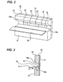
- a light source 10 is mounted to the center of a front surface of the bracket 7. As shown in FIG. 2 , the light source 10 includes a circuit board 11, a plurality of semiconductor light emitting devices 12, 12... a lower reflector 13 and an upper reflector 14.
- LED Light Emitting Diode
- the semiconductor light emitting devices 12, 12,... serve as a surface-emitting light source, and are provided in parallel in the left-right direction in a state where a light emitting surface faces a front direction.
- Drive current is separately supplied to each of the semiconductor light emitting devices 12, 12,... from a lighting circuit (not shown)
- the semiconductor light emitting devices 12, 12... to which the drive current is supplied are turned on and the semiconductor light emitting devices 12, 12... to which the drive current is not supplied are maintained in a turned off state.
- a control for changing the current value of drive current supplied from the lighting circuit can be separately performed.
- the lower reflector 13 and the upper reflector 14 are respectively provided in the lower side and the upper side with the semiconductor light emitting devices 12 sandwiched therebetween.
- the lower reflector 13 and the upper reflector 14 respectively include a reflection surface 13a substantially facing upward and a reflection surface 14a substantially facing downward.
- the reflection surface 13a and the reflection surface 14a are respectively continuous to a lower edge and an upper edge of the semiconductor light emitting devices 12, 12, ...
- the reflection surface 13a of the lower reflector 13 is formed in a paraboloidal surface, for example and the reflection surface 14a of the upper reflector 14 is formed in a hyperboloidal surface, for example.
- the light reflected by the reflection surface 13a is directed more upward than the light reflected by the reflection surface 14a.
- a movable shade 15 is provided on the lamp unit 6.
- the movable shade 15 is configured to cover or uncover the reflection surface 13a of the lower reflector 13 and has a size enough to cover the entire surface of the reflection surface 13a.
- the shielding range of the light which is emitted from the semiconductor light emitting devices 12 and directed to the reflection surface 13a of the lower reflector 13 is changed according to the moving position of the movable shade.
- a lens holder 16 is disposed on a front surface of the bracket 7 (see, FIG. 1 ).
- the lens holder 16 has a substantially cylindrical shape having a through hole in a front-rear direction and is disposed on the bracket 7 to cover the light source 10.
- a projector lens 17 is mounted on a front surface of the lens holder 16.
- the projector lens 17 is configured to reverse an image on a focal plane including a rear focal point and to project the light emitted from the semiconductor light emitting devices 12 toward the front area.
- the lamp unit 6 is configured to be tilted in the left-right direction and the front-rear direction by the optical axis adjustment mechanism.
- the optical axis adjustment mechanism includes aiming screws 18, 18 (only one aiming screw 18 is shown in FIG. 1 ) and a leveling actuator 19.
- the aiming screws 18, 18 are separated from each other in a left-right direction and the front ends thereof are respectively screwed to the supported parts 7a, 7a of the upper side of the bracket 7.
- the leveling actuator 19 includes a driving part 19a and a shaft part 19b protruding from the driving part 19a.
- the front end of the shaft part 19b is screwed to the supported parts 7a of the lower side of the bracket 7.
- the lamp unit 6 is tilted about the supported parts 7a, 7a as a pivot point, other than the part to which the aiming screw 18 is screwed, and thus optical axis adjustment (leveling adjustment) of the lamp unit 6 is performed.
- the lamp unit 6 is tilted about the supported parts 7a, 7a as a pivot point, other than the part to which the shaft part 19b is screwed and thus optical axis adjustment (leveling adjustment) of the lamp unit 6 is performed.
- a detection camera (not shown) including an imaging device such as CCD (Charge Coupled Device) is mounted on a vehicle.
- the irradiation area of the vehicle headlamp 1 is captured by the detection camera periodically.
- an image data is generated and then an image processing is carried out to detect the presence or the presence position of an object existing at the irradiation area such as a preceding vehicle, an oncoming vehicle, a pedestrian, a sign or a signal.
- the vehicle headlamp 1 configured as described above, it is possible to change the light distribution pattern formed by light which are emitted from the left lamp 1A and the right lamp 1B by controlling turning on/off of the semiconductor light emitting devices 12 and light shielding range by the movable shade 15.
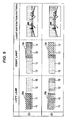
- a dotted area represents an area in which the semiconductor light emitting device 12 is turned on and a hatched area corresponds to the movable shade 15 and also represents an area in which light is shielded by the movable shade 15. Accordingly, a light irradiation area of the light distribution pattern corresponds to an area in which the semiconductor light emitting device 12 is turned on and is not shielded by the movable shade 15.
- FIG. 4(A) shows a case where the same control of the turning on/off of the semiconductor light emitting devices 12 is made in the left lamp 1A and the right lamp 1B and the same control of the light shielding range by the movable shade 15 is made in the left lamp 1A and the right lamp 1B.
- a portion of the semiconductor light emitting devices 12 is turned off and light which is irradiated upward is respectively shielded by the movable shades 15, 15.
- FIG. 4(B) shows a case where a control of the turning on/off of the semiconductor light emitting devices 12 is different from each other in the left lamp 1A and the right lamp 1B and a control of the light shielding range by the movable shade 15 is made in the left lamp 1A.
- different portion of the semiconductor light emitting devices 12 is respectively turned off in each of the left lamp 1A and the right lamp 1B and light which is irradiated upward is shielded by the movable shade 15 in the left lamp 1A.
- a portion of the semiconductor light emitting devices 12 may be turned off in the left lamp 1A and the right lamp 1B and light may be shielded by the movable shades 15 in the left lamp 1A.
- FIG. 4(C) shows a case where a control of the turning on/off of the semiconductor light emitting devices 12 is different from each other in the left lamp 1A and the right lamp 1B and a control of the light shielding range by the movable shade 15 is different from each other in the left lamp 1A and the right lamp 1B.
- different portion of the semiconductor light emitting devices 12 is respectively turned off in each of the left lamp 1A and the right lamp 1B and light which is irradiated upward is respectively shielded by the movable shades 15, 15 in the left lamp 1A and the right lamp 1B.
- the movable shades 15, 15 have a size enough to cover the entire reflection surface 13a of the lower reflector 13. Meanwhile, a control of the light shielding range may be performed by the movable shades 15A, 15A having a size enough to cover at least a portion (for example, half portion) of the reflection surfaces 13a, 13a of the lower reflectors 13, 13 in the left lamp 1A and the right lamp 1B, as shown in FIG. 5 .
- the movable shade 15A in the left lamp 1A is configured to cover a left half portion, for example, of the reflection surface 13a of the lower reflector 13 and the movable shade 15A in the right lamp 1B is configured to cover a right half portion, for example, of the reflection surface 13a of the lower reflector 13.
- the movable shade 15A in the left lamp 1A may be configured to cover or uncover a right half portion of the reflection surface 13a of the lower reflector 13 and the movable shade 15A in the right lamp 1B may be configured to cover or uncover a left half portion of the reflection surface 13a of the lower reflector 13.
- FIG. 6(D) shows a case where all of the semiconductor light emitting devices 12 in a range which cannot be shielded by the movable shades 15A, 15A are turned off, a control of the turning on/off of the semiconductor light emitting devices 12 is different from each other in the left lamp 1A and the right lamp 1B and control of the light shielding range using the movable shades 15A, 15A is made in the left lamp 1A and the right lamp 1B.
- different portion of the semiconductor light emitting devices 12 is respectively turned off in each of the left lamp 1A and the right lamp 1B and light which is irradiated upward is respectively shielded by the movable shades 15A, 15A in the left lamp 1A and the right lamp 1B.
- FIG. 6(E) shows a case where a control of the turning on/off of the semiconductor light emitting devices 12 is different from each other in the left lamp 1A and the right lamp 1B and a control of the light shielding range by the movable shades 15A, 15A is made in the left lamp 1A and the right lamp 1B.
- different portion of the semiconductor light emitting devices 12 is respectively turned off in each of the left lamp 1A and the right lamp 1B and light which is irradiated upward is respectively shielded by the movable shades 15A, 15A in the left lamp 1A and the right lamp 1B.
- the size of the movable shades 15A, 15A is small, a driving force of a drive mechanism for the movable shades 15A, 15A can be reduced and the size of the drive mechanism can be miniaturized and thus it is possible to reduce a manufacturing cost of the vehicle headlamp 1.
- the light shielding range may be controlled by covering or uncovering the entire portion or a portion of the reflection surface 13a of the lower reflector 13 using the movable shades 15A, 15A
- the light shielding range may be controlled by covering or uncovering the entire portion of the reflection surface 13a of the lower reflector 13 in the left lamp 1A using the movable shade 15 and by covering or uncovering the entire portion of the reflection surface 14a of the upper reflector 14 in the right lamp 1B using the movable shade 15B, as shown in FIG. 7 .
- a control of the light shielding range may be performed by the movable shade 15B to cover/uncover the reflection surface 14a of the upper reflector 14 in the left lamp 1A and the movable shade 15 to cover/uncover the reflection surface 13a of the lower reflector 13 in the right lamp 1B.
- FIG. 8(F) shows a case where a control of the light shielding range by the movable shades 15, 15B is made in the left lamp 1A and the right lamp 1B.
- all of the semiconductor light emitting devices 12 are turned on in the left lamp 1A and the right lamp 1B, light which is irradiated upward is shielded by the movable shade 15 in the left lamp 1A, and light which is irradiated downward is shielded by the movable shade 15B in the right lamp 1B.
- FIG. 8(G) shows a case where a control of the turning on/off of the semiconductor light emitting devices 12 is different from each other in the left lamp 1A and the right lamp 1B and a control of the light shielding range by the movable shades 15, 15B is made in the left lamp 1A and the right lamp 1B.
- a portion of the semiconductor light emitting devices 12 is turned off in the left lamp 1A, all of the semiconductor light emitting devices 12 is turned on in the right lamp 1B, light which is irradiated upward is shielded by the movable shade 15 in the left lamp 1A and light which is irradiated downward is shielded by the movable shade 15B in the right lamp 1B.
- FIG. 8(H) shows a case where a control of the turning on/off of the semiconductor light emitting devices 12 is different from each other in the left lamp 1A and the right lamp 1B and a control of the light shielding range by the movable shades 15, 15B is made in the left lamp 1A and the right lamp 1B.
- all of the semiconductor light emitting devices 12 are turned on in the left lamp 1A, a portion of the semiconductor light emitting devices 12 is turned off in the right lamp 1B, light which is irradiated upward is shielded by the movable shade 15 in the left lamp 1A and light which is irradiated downward is shielded by the movable shade 15B in the right lamp 1B.
- FIG. 8(I) shows a case where a control of the turning on/off of the semiconductor light emitting devices 12 is different from each other in the left lamp 1A and the right lamp 1B and a control of the light shielding range by the movable shades 15, 15B is made in the left lamp 1A and the right lamp 1B.
- different portion of the semiconductor light emitting devices 12 is respectively turned off in each of the left lamp 1A and the right lamp 1B, light which is irradiated upward is shielded by the movable shade 15 in the left lamp 1A and light which is irradiated downward is shielded by the movable shade 15B in the right lamp 1B.
- the movable shades 15, 15B are configured to cover/uncover the reflection surface 13a of the lower reflector 13 and the reflection surface 14a of the upper reflector 14, it is possible to form a light distribution pattern which can be divided in an upper-lower direction without separating the semiconductor light emitting devices 12 from each other in the upper-lower direction. Further, it is possible to perform a proper light distribution control according to the driving condition of the vehicle by widening the irradiation range in the upper-lower direction.
- the light distribution pattern is formed by controlling turning on/off of the semiconductor light emitting devices 12 and light shielding range using the movable shades 15, 15A, 15B, it is possible to form a light distribution pattern with partially different brightness by controlling the current value of drive current for the semiconductor light emitting devices 12, respectively.
- a range of the light distribution pattern controlled by the movable shade 15 and a range of the light distribution pattern controlled by the movable shade 15B are not overlapped from each other.
- the brightness change which is caused by the change in the current value of drive current for the semiconductor light emitting devices 12 does not affect on light emitted from the semiconductor light emitting devices 12 which are not subjected to the change in the current value of drive current.
- the light distribution pattern is formed by controlling turning on/off of the semiconductor light emitting devices 12 and light shielding range using the movable shades 15, 15A, 15B, it is possible to perform a proper light distribution control according to the driving condition of the vehicle in order to improve the visibility and prevent the occurrence of the glare.
- the movable shades 15, 15A, 15B are respectively provided to each of the lamp units 6, 6, it is possible to improve a degree of light distribution control.
Abstract

Description
- The present invention relates to a vehicle headlamp and, more particularly, to a vehicle headlamp which is capable of making a desired light distribution pattern by turning on/off a plurality of semiconductor light emitting devices and moving a movable shade and performing a light distribution control properly according to a driving condition of a vehicle.
- A vehicle headlamp is known in which a light source is arranged in a lamp outer housing that is formed by a cover and a lamp body and a movable shade changes a shielding range of a light emitted from the light source and thus a light distribution pattern can be switched (see
JP-A-2011-29121 - In the vehicle headlamp disclosed in
JP-A-2011-29121 - However, in the vehicle headlamp disclosed in
JP-A-2011-29121 - Accordingly, visibility for the preceding vehicle, the oncoming vehicle, the pedestrian, the sign, the signal or the like might be degraded and also might be given glare.
- It is an illustrative aspect of the present invention to provide a vehicle headlamp capable of performing a proper light distribution control according to the driving condition of the vehicle in order to improve the visibility and prevent the occurrence of the glare.
- According to a first aspect of the invention, there is provided a vehicle headlamp (1) comprising a light source (10). The light source (10) comprises: a circuit board (11) whose surface is directed toward a front area of the vehicle headlamp (1); a plurality of semiconductor light emitting elements (12) arranged in a line on the surface of the circuit board and each configured to emit light; an upper reflector (14) disposed on the surface of the circuit board and configured to reflect the light emitted from the semiconductor light emitting elements toward the front area; a lower reflector (13) disposed on the surface of the circuit board and configured to reflect the light emitted from the semiconductor light emitting elements toward the front area, wherein the semiconductor light emitting elements are disposed between the upper reflector and the lower reflector; and a movable shade (15) configured to move in a front-rear direction of the vehicle headlamp so as to cover/uncover one of the upper reflector (14) and the lower reflector (13), wherein when the movable shade (15) covers said one of the upper reflector (14) and the lower reflector (13), the light which is incident on said one of the upper reflector (14) and the lower reflector (13) is blocked by the movable shade. The vehicle headlamp is configured to form a certain light distribution pattern by turning on/off of the respective semiconductor light emitting elements and moving the movable shade in the front-rear direction.
- According to a second aspect of the present invention, the movable shade (15) is configured to cover/uncover the lower reflector (13).
- According to a third aspect of the present invention, the movable shade (15) is configured to cover/uncover the upper reflector (14).
- According to a fourth aspect of the present invention, when the movable shade (15) entirely covers a reflection surface of said one of the upper reflector (14) and the lower reflector (13).
- According to a fifth aspect of the present invention, when the movable shade (15) partially covers a reflection surface of said one of the upper reflector (14) and the lower reflector (13).
- According to a sixth aspect of the present invention, a reflection surface (13a) of the lower surface (13) is formed in a paraboloidal surface, and a reflection surface (14a) of the upper surface (14) is formed in a hyperboloidal surface.
- According to a seventh aspect of the present invention, a light distribution pattern control system. The light distribution pattern control system comprises: a left lamp (1A) and a right lamp (1B), each of which has the same configuration as the vehicle headlamp as described above. The left lamp (1A) is configured to form a first light distribution pattern by turning on/off of the respective semiconductor light emitting elements and moving the movable shade in the front-rear direction. The right lamp (1B) is configured to form a second light distribution pattern by turning on/off of the respective semiconductor light emitting elements and moving the movable shade in the front-rear direction. A light distribution pattern of the light distribution pattern control system is formed by combining the first and second light distribution patterns.
-
-
FIG. 1 is a schematic longitudinal sectional view of a vehicle headlamp according to an embodiment of the present invention; -
FIG. 2 is a perspective view showing a light source and a movable shade; -
FIG.3 is a cross-sectional view showing the light source and the movable shade; -
FIG. 4 is a schematic view showing how the light distribution pattern can be controlled by the movable shade; -
FIG. 5 is a perspective view showing the light source and the moveable shade which is configured to cover a half portion of a reflection surface of the reflector, in a left lamp and a right lamp; -
FIG. 6 is a schematic view showing how the light distribution pattern can be controlled by the configuration shown inFIG. 5 ; -
FIG. 7 is a perspective view showing the light source and the moveable shade which is disposed to cover the upper reflector or the lower reflector, in the left lamp and the right lamp; and -
FIG. 8 is a schematic view showing how the light distribution pattern can be controlled by the configuration shown inFIG. 7 . - Hereinafter, the same or equivalent components, members, and signals, which are shown in the respective drawings, are denoted by the same reference numerals, and the repeated description thereof will be appropriately omitted. Further, some of members, which are not important in the description, will be omitted in the respective drawings.
- A
vehicle headlamp 1 includes aleft lamp 1A located at a left side and aright lamp 1 B located at a right side (see,FIG. 1 ). - The
left lamp 1A and theright lamp 1B are respectively configured so that alamp body 2 whose front side is opened and acover 3 covering the front side of thelamp body 2 forms a lamp outer housing 4 and an interior of the lamp outer housing 4 is configured as alamp chamber 5 and alamp unit 6 is disposed in thelamp chamber 5. - In the
lamp unit 6, certain components are mounted on abracket 7 attached to thelamp chamber 5 and thelamp unit 6 can be tilted in a left-right direction and a front-rear direction by an optical axis adjustment mechanism, which will be described later. - The
bracket 7 is formed from a metal material with high thermal conductivity and is provided at its both upper and lower ends with supportedparts FIG. 1 ).Heat radiation fins bracket 7. Aheat radiating fan 9 is mounted on a rear surface of the heat radiation fins 8, 8,.... - A
light source 10 is mounted to the center of a front surface of thebracket 7. As shown inFIG. 2 , thelight source 10 includes acircuit board 11, a plurality of semiconductorlight emitting devices lower reflector 13 and anupper reflector 14. - For example, LED (Light Emitting Diode) may be used as the semiconductor
light emitting devices light emitting devices - Drive current is separately supplied to each of the semiconductor
light emitting devices light emitting devices light emitting devices - Further, for each of the semiconductor
light emitting devices - As shown in
FIGS. 2 and 3 , thelower reflector 13 and theupper reflector 14 are respectively provided in the lower side and the upper side with the semiconductorlight emitting devices 12 sandwiched therebetween. Thelower reflector 13 and theupper reflector 14 respectively include areflection surface 13a substantially facing upward and areflection surface 14a substantially facing downward. Thereflection surface 13a and thereflection surface 14a are respectively continuous to a lower edge and an upper edge of the semiconductorlight emitting devices - The
reflection surface 13a of thelower reflector 13 is formed in a paraboloidal surface, for example and thereflection surface 14a of theupper reflector 14 is formed in a hyperboloidal surface, for example. The light reflected by thereflection surface 13a is directed more upward than the light reflected by thereflection surface 14a. - A
movable shade 15 is provided on thelamp unit 6. Themovable shade 15 is configured to cover or uncover thereflection surface 13a of thelower reflector 13 and has a size enough to cover the entire surface of thereflection surface 13a. As themovable shade 15 moves, the shielding range of the light which is emitted from the semiconductorlight emitting devices 12 and directed to thereflection surface 13a of thelower reflector 13 is changed according to the moving position of the movable shade. - A
lens holder 16 is disposed on a front surface of the bracket 7 (see,FIG. 1 ). Thelens holder 16 has a substantially cylindrical shape having a through hole in a front-rear direction and is disposed on thebracket 7 to cover thelight source 10. - A
projector lens 17 is mounted on a front surface of thelens holder 16. Theprojector lens 17 is configured to reverse an image on a focal plane including a rear focal point and to project the light emitted from the semiconductorlight emitting devices 12 toward the front area. - As mentioned above, the
lamp unit 6 is configured to be tilted in the left-right direction and the front-rear direction by the optical axis adjustment mechanism. - The optical axis adjustment mechanism includes aiming
screws 18, 18 (only one aimingscrew 18 is shown inFIG. 1 ) and aleveling actuator 19. - The aiming
screws parts bracket 7. - The leveling
actuator 19 includes a drivingpart 19a and ashaft part 19b protruding from thedriving part 19a. The front end of theshaft part 19b is screwed to the supportedparts 7a of the lower side of thebracket 7. - In the
vehicle headlamp 1, as the aimingscrew 18 is rotated, thelamp unit 6 is tilted about the supportedparts screw 18 is screwed, and thus optical axis adjustment (leveling adjustment) of thelamp unit 6 is performed. - Further, as the
shaft part 19b of the levelingactuator 19 is rotated by the driving force of the drivingpart 19a, thelamp unit 6 is tilted about the supportedparts shaft part 19b is screwed and thus optical axis adjustment (leveling adjustment) of thelamp unit 6 is performed. - For example, a detection camera (not shown) including an imaging device such as CCD (Charge Coupled Device) is mounted on a vehicle. The irradiation area of the
vehicle headlamp 1 is captured by the detection camera periodically. As the irradiation area is captured by the detection camera, an image data is generated and then an image processing is carried out to detect the presence or the presence position of an object existing at the irradiation area such as a preceding vehicle, an oncoming vehicle, a pedestrian, a sign or a signal. - In the
vehicle headlamp 1 configured as described above, it is possible to change the light distribution pattern formed by light which are emitted from theleft lamp 1A and theright lamp 1B by controlling turning on/off of the semiconductorlight emitting devices 12 and light shielding range by themovable shade 15. - Hereinafter, each of the light distribution patterns formed by the above-mentioned control will be described with reference to
Fig. 4 . Further, inFig. 4 , a dotted area represents an area in which the semiconductorlight emitting device 12 is turned on and a hatched area corresponds to themovable shade 15 and also represents an area in which light is shielded by themovable shade 15. Accordingly, a light irradiation area of the light distribution pattern corresponds to an area in which the semiconductorlight emitting device 12 is turned on and is not shielded by themovable shade 15. -
FIG. 4(A) shows a case where the same control of the turning on/off of the semiconductorlight emitting devices 12 is made in theleft lamp 1A and theright lamp 1B and the same control of the light shielding range by themovable shade 15 is made in theleft lamp 1A and theright lamp 1B. In case ofFIG. 4(A) , a portion of the semiconductorlight emitting devices 12 is turned off and light which is irradiated upward is respectively shielded by themovable shades - In case of
FIG. 4(A) , it is possible to prevent glare from being given to pedestrians or occupants of oncoming vehicle. -
FIG. 4(B) shows a case where a control of the turning on/off of the semiconductorlight emitting devices 12 is different from each other in theleft lamp 1A and theright lamp 1B and a control of the light shielding range by themovable shade 15 is made in theleft lamp 1A. In case ofFIG. 4(B) , different portion of the semiconductorlight emitting devices 12 is respectively turned off in each of theleft lamp 1A and theright lamp 1B and light which is irradiated upward is shielded by themovable shade 15 in theleft lamp 1A. - In case of
FIG. 4(B) , while a wide irradiation range is secured, it is possible to prevent glare from being given to pedestrians or occupants of oncoming vehicle. - To contrary to the above, a portion of the semiconductor
light emitting devices 12 may be turned off in theleft lamp 1A and theright lamp 1B and light may be shielded by themovable shades 15 in theleft lamp 1A. - In case of
FIG. 4(B) , light which is irradiated upward is shielded by themovable shades 15 in either theleft lamp 1A or theright lamp 1B. Accordingly, light shielding control using themovable shade 15 is made in either theleft lamp 1A or theright lamp 1B and, themovable shade 15 is disposed in either theleft lamp 1A or theright lamp 1B. -
FIG. 4(C) shows a case where a control of the turning on/off of the semiconductorlight emitting devices 12 is different from each other in theleft lamp 1A and theright lamp 1B and a control of the light shielding range by themovable shade 15 is different from each other in theleft lamp 1A and theright lamp 1B. In case ofFIG. 4(C) , different portion of the semiconductorlight emitting devices 12 is respectively turned off in each of theleft lamp 1A and theright lamp 1B and light which is irradiated upward is respectively shielded by themovable shades left lamp 1A and theright lamp 1B. - In case of
FIG. 4(C) , while a wide irradiation range is secured, it is possible to prevent glare from being given to pedestrians or occupants of oncoming vehicle. Further, when a light spot emitted from a traffic light is detected, light is not irradiated to the light spot and thus visibility for the light is improved. - In the above-described embodiment, there has been described a case where the
movable shades entire reflection surface 13a of thelower reflector 13. Meanwhile, a control of the light shielding range may be performed by themovable shades lower reflectors left lamp 1A and theright lamp 1B, as shown inFIG. 5 . - The
movable shade 15A in theleft lamp 1A is configured to cover a left half portion, for example, of thereflection surface 13a of thelower reflector 13 and themovable shade 15A in theright lamp 1B is configured to cover a right half portion, for example, of thereflection surface 13a of thelower reflector 13. - On the contrary, the
movable shade 15A in theleft lamp 1A may be configured to cover or uncover a right half portion of thereflection surface 13a of thelower reflector 13 and themovable shade 15A in theright lamp 1B may be configured to cover or uncover a left half portion of thereflection surface 13a of thelower reflector 13. - Control of the light distribution pattern using the
movable shades FIG. 6 ). -
FIG. 6(D) shows a case where all of the semiconductorlight emitting devices 12 in a range which cannot be shielded by themovable shades light emitting devices 12 is different from each other in theleft lamp 1A and theright lamp 1B and control of the light shielding range using themovable shades left lamp 1A and theright lamp 1B. In case ofFIG. 6(D) , different portion of the semiconductorlight emitting devices 12 is respectively turned off in each of theleft lamp 1A and theright lamp 1B and light which is irradiated upward is respectively shielded by themovable shades left lamp 1A and theright lamp 1B. - In case of FIG. 4(D), it is possible to prevent glare from being given to pedestrians or occupants of oncoming vehicle.
-
FIG. 6(E) shows a case where a control of the turning on/off of the semiconductorlight emitting devices 12 is different from each other in theleft lamp 1A and theright lamp 1B and a control of the light shielding range by themovable shades left lamp 1A and theright lamp 1B. In case of FIG. 6(B), different portion of the semiconductorlight emitting devices 12 is respectively turned off in each of theleft lamp 1A and theright lamp 1B and light which is irradiated upward is respectively shielded by themovable shades left lamp 1A and theright lamp 1B. - In case of
FIG. 6(E) , while a wide irradiation range is secured, it is possible to prevent glare from being given to pedestrians or occupants of oncoming vehicle. - Since the size of the
movable shades movable shades vehicle headlamp 1. - Further, although there has been described a case where the light shielding range is controlled by covering or uncovering the entire portion or a portion of the
reflection surface 13a of thelower reflector 13 using themovable shades reflection surface 13a of thelower reflector 13 in theleft lamp 1A using themovable shade 15 and by covering or uncovering the entire portion of thereflection surface 14a of theupper reflector 14 in theright lamp 1B using themovable shade 15B, as shown inFIG. 7 . - Further, a control of the light shielding range may be performed by the
movable shade 15B to cover/uncover thereflection surface 14a of theupper reflector 14 in theleft lamp 1A and themovable shade 15 to cover/uncover thereflection surface 13a of thelower reflector 13 in theright lamp 1B. - Controlling of the light distribution pattern using the
movable shades FIG. 8 . -
FIG. 8(F) shows a case where a control of the light shielding range by themovable shades left lamp 1A and theright lamp 1B. In case ofFIG. 8(F) , all of the semiconductorlight emitting devices 12 are turned on in theleft lamp 1A and theright lamp 1B, light which is irradiated upward is shielded by themovable shade 15 in theleft lamp 1A, and light which is irradiated downward is shielded by themovable shade 15B in theright lamp 1B. - In case of
FIG. 8(F) , it is possible to prevent glare from being given to occupants of oncoming vehicle or preceding vehicle. -
FIG. 8(G) shows a case where a control of the turning on/off of the semiconductorlight emitting devices 12 is different from each other in theleft lamp 1A and theright lamp 1B and a control of the light shielding range by themovable shades left lamp 1A and theright lamp 1B. In case ofFIG. 8(G) , a portion of the semiconductorlight emitting devices 12 is turned off in theleft lamp 1A, all of the semiconductorlight emitting devices 12 is turned on in theright lamp 1B, light which is irradiated upward is shielded by themovable shade 15 in theleft lamp 1A and light which is irradiated downward is shielded by themovable shade 15B in theright lamp 1B. - In case of
FIG. 8(G) , while a wide irradiation range is secured, it is possible to prevent glare from being given to occupants of oncoming vehicle or preceding vehicle. -
FIG. 8(H) shows a case where a control of the turning on/off of the semiconductorlight emitting devices 12 is different from each other in theleft lamp 1A and theright lamp 1B and a control of the light shielding range by themovable shades left lamp 1A and theright lamp 1B. In case ofFIG. 8(H) , all of the semiconductorlight emitting devices 12 are turned on in theleft lamp 1A, a portion of the semiconductorlight emitting devices 12 is turned off in theright lamp 1B, light which is irradiated upward is shielded by themovable shade 15 in theleft lamp 1A and light which is irradiated downward is shielded by themovable shade 15B in theright lamp 1B. - In case of
FIG. 8(H) , while a wide irradiation range is secured, it is possible to prevent from glare being given to occupants of oncoming vehicle or preceding vehicle. -
FIG. 8(I) shows a case where a control of the turning on/off of the semiconductorlight emitting devices 12 is different from each other in theleft lamp 1A and theright lamp 1B and a control of the light shielding range by themovable shades left lamp 1A and theright lamp 1B. In case ofFIG. 8(I) , different portion of the semiconductorlight emitting devices 12 is respectively turned off in each of theleft lamp 1A and theright lamp 1B, light which is irradiated upward is shielded by themovable shade 15 in theleft lamp 1A and light which is irradiated downward is shielded by themovable shade 15B in theright lamp 1B. - In case of
FIG. 8(I) , while a wide irradiation range is secured, it is possible to prevent glare from being given to occupants of oncoming vehicle or preceding vehicle. - As mentioned above, since the
movable shades reflection surface 13a of thelower reflector 13 and thereflection surface 14a of theupper reflector 14, it is possible to form a light distribution pattern which can be divided in an upper-lower direction without separating the semiconductorlight emitting devices 12 from each other in the upper-lower direction. Further, it is possible to perform a proper light distribution control according to the driving condition of the vehicle by widening the irradiation range in the upper-lower direction. - In a case where the light distribution pattern is formed by controlling turning on/off of the semiconductor
light emitting devices 12 and light shielding range using themovable shades light emitting devices 12, respectively. - Further, in the control (see,
FIGS. 7 and 8 ) using themovable shades movable shade 15 and a range of the light distribution pattern controlled by themovable shade 15B are not overlapped from each other. - Accordingly, the brightness change which is caused by the change in the current value of drive current for the semiconductor
light emitting devices 12 does not affect on light emitted from the semiconductorlight emitting devices 12 which are not subjected to the change in the current value of drive current. - As described above, since in the
vehicle headlamp 1, the light distribution pattern is formed by controlling turning on/off of the semiconductorlight emitting devices 12 and light shielding range using themovable shades - Further, since the
movable shades lamp units - All of the shapes and structures of the respective portions shown in the above-mentioned embodiment are merely illustrative when the invention is embodied, and the technical scope of the invention should not be interpreted in a limited way.
Claims (7)
- A vehicle headlamp (1), comprising:a light source (10) comprising:a circuit board (11) whose surface is directed toward a front area of the vehicle headlamp (1);a plurality of semiconductor light emitting elements (12) arranged in a line on the surface of the circuit board and each configured to emit light;an upper reflector (14) disposed on the surface of the circuit board and configured to reflect the light emitted from the semiconductor light emitting elements toward the front area;a lower reflector (13) disposed on the surface of the circuit board and configured to reflect the light emitted from the semiconductor light emitting elements toward the front area, wherein the semiconductor light emitting elements are disposed between the upper reflector and the lower reflector; anda movable shade (15) configured to move in a front-rear direction of the vehicle headlamp so as to cover/uncover one of the upper reflector (14) and the lower reflector (13), wherein when the movable shade (15) covers said one of the upper reflector (14) and the lower reflector (13), the light which is incident on said one of the upper reflector (14) and the lower reflector (13) is blocked by the movable shade,wherein the vehicle headlamp is configured to form a certain light distribution pattern by turning on/off of the respective semiconductor light emitting elements and moving the movable shade in the front-rear direction.
- The vehicle headlamp of claim 1, wherein the movable shade (15) is configured to cover/uncover the lower reflector (13).
- The vehicle headlamp of claim 1, wherein the movable shade (15) is configured to cover/uncover the upper reflector (14).
- The vehicle headlamp of any one of claims 1 to 3, wherein the movable shade (15) entirely covers a reflection surface of said one of the upper reflector (14) and the lower reflector (13).
- The vehicle headlamp of any one of claims 1 to 3, wherein the movable shade (15) partially covers a reflection surface of said one of the upper reflector (14) and the lower reflector (13).
- The vehicle headlamp of any one of claims 1 to 5, wherein a reflection surface (13a) of the lower surface (13) is formed in a paraboloidal surface, and a reflection surface (14a) of the upper surface (14) is formed in a hyperboloidal surface.
- A light distribution pattern control system, comprising:a left lamp (1A) and a right lamp (1B), each of which has the same configuration as the vehicle headlamp of claim 1,wherein the left lamp (1A) is configured to form a first light distribution pattern by turning on/off of the respective semiconductor light emitting elements and moving the movable shade in the front-rear direction, andwherein the right lamp (1B) is configured to form a second light distribution pattern by turning on/off of the respective semiconductor light emitting elements and moving the movable shade in the front-rear direction, andwherein a light distribution pattern of the light distribution pattern control system is formed by combining the first and second light distribution patterns.
Applications Claiming Priority (1)
| Application Number | Priority Date | Filing Date | Title |
|---|---|---|---|
| JP2011236958A JP5828424B2 (en) | 2011-10-28 | 2011-10-28 | Vehicle headlamp |
Publications (2)
| Publication Number | Publication Date |
|---|---|
| EP2586659A1 true EP2586659A1 (en) | 2013-05-01 |
| EP2586659B1 EP2586659B1 (en) | 2020-08-12 |
Family
ID=47227452
Family Applications (1)
| Application Number | Title | Priority Date | Filing Date |
|---|---|---|---|
| EP12190134.2A Active EP2586659B1 (en) | 2011-10-28 | 2012-10-26 | Vehicle headlamp |
Country Status (3)
| Country | Link |
|---|---|
| EP (1) | EP2586659B1 (en) |
| JP (1) | JP5828424B2 (en) |
| CN (1) | CN103090287B (en) |
Cited By (5)
| Publication number | Priority date | Publication date | Assignee | Title |
|---|---|---|---|---|
| EP2546567A3 (en) * | 2011-07-12 | 2014-06-11 | Koito Manufacturing Co., Ltd. | Vehicle headlight |
| EP3028897A1 (en) * | 2014-12-01 | 2016-06-08 | Automotive Lighting Reutlingen GmbH | Method for generating a front light distribution for a motor vehicle and motor vehicle lighting device |
| EP3201519A1 (en) * | 2014-10-02 | 2017-08-09 | Valeo Vision | Lighting system with optimised intensity profile for motor vehicle headlight |
| EP3489083A1 (en) * | 2017-11-22 | 2019-05-29 | Stanley Electric Co., Ltd. | Vehicle headlight |
| EP3859203A1 (en) * | 2020-01-31 | 2021-08-04 | Hyundai Mobis Co., Ltd. | Headlamp for automobile and automobile with such a headlamp |
Families Citing this family (10)
| Publication number | Priority date | Publication date | Assignee | Title |
|---|---|---|---|---|
| JP6211817B2 (en) * | 2013-06-10 | 2017-10-11 | 株式会社小糸製作所 | Vehicle lighting |
| JP6132684B2 (en) * | 2013-07-10 | 2017-05-24 | 株式会社小糸製作所 | Vehicle lighting |
| US10300840B2 (en) * | 2014-02-04 | 2019-05-28 | Koito Manufacturing Co., Ltd. | Vehicle lamp control system |
| US10018325B2 (en) * | 2015-03-31 | 2018-07-10 | Seoul Semiconductor Co., Ltd. | Light device of vehicle |
| DE102015013191A1 (en) * | 2015-10-10 | 2017-04-13 | Daimler Ag | Method for operating a lighting unit and lighting unit |
| JP6812120B2 (en) * | 2016-03-25 | 2021-01-13 | 株式会社小糸製作所 | Vehicle lighting fixtures and vehicles equipped with the vehicle lighting fixtures |
| JP6782559B2 (en) * | 2016-05-13 | 2020-11-11 | 株式会社小糸製作所 | Vehicle headlights |
| KR101830663B1 (en) * | 2016-07-06 | 2018-02-21 | 엘지전자 주식회사 | Vehicle lamp and control metohd thereof |
| CN106016128A (en) * | 2016-07-08 | 2016-10-12 | 吴富双 | Integrated motor vehicle headlight structure |
| EP3492317A4 (en) * | 2016-07-29 | 2020-07-22 | Koito Manufacturing Co., Ltd. | Vehicle lighting system, vehicle system, and vehicle |
Citations (8)
| Publication number | Priority date | Publication date | Assignee | Title |
|---|---|---|---|---|
| DE19756437A1 (en) * | 1997-12-18 | 1999-06-24 | Bosch Gmbh Robert | Vehicle headlamp with high and dipped beam settings |
| EP2101107A2 (en) * | 2008-03-12 | 2009-09-16 | Koito Manufacturing Co., Ltd | Vehicle headlamp apparatus |
| EP2213935A1 (en) * | 2009-01-30 | 2010-08-04 | Ichikoh Industries Limited | Vehicle headlamp |
| EP2282110A2 (en) * | 2009-08-03 | 2011-02-09 | Koito Manufacturing Co., Ltd | Vehicular lamp |
| JP2011029121A (en) | 2009-07-29 | 2011-02-10 | Koito Mfg Co Ltd | Headlamp for vehicle |
| JP2011124100A (en) * | 2009-12-10 | 2011-06-23 | Koito Mfg Co Ltd | Lighting fixture for vehicle |
| US20110235349A1 (en) * | 2010-03-25 | 2011-09-29 | Yoshiaki Nakaya | Vehicle light and method for controlling light distribution |
| EP2455656A2 (en) * | 2010-11-18 | 2012-05-23 | Koito Manufacturing Co., Ltd. | Vehicle headlamp |
Family Cites Families (6)
| Publication number | Priority date | Publication date | Assignee | Title |
|---|---|---|---|---|
| JP4343003B2 (en) * | 2004-03-31 | 2009-10-14 | 株式会社小糸製作所 | Vehicle headlamp |
| JP4953922B2 (en) * | 2007-05-30 | 2012-06-13 | 株式会社小糸製作所 | Vehicle headlamp |
| JP2009231020A (en) * | 2008-03-21 | 2009-10-08 | Koito Mfg Co Ltd | Headlight device for vehicle |
| JP5199781B2 (en) * | 2008-08-11 | 2013-05-15 | 株式会社小糸製作所 | Vehicle headlamp device |
| JP5398507B2 (en) * | 2009-12-16 | 2014-01-29 | 株式会社小糸製作所 | Vehicle headlamp device |
| JP5883587B2 (en) * | 2011-07-12 | 2016-03-15 | 株式会社小糸製作所 | Vehicle headlamp |
-
2011
- 2011-10-28 JP JP2011236958A patent/JP5828424B2/en active Active
-
2012
- 2012-10-26 EP EP12190134.2A patent/EP2586659B1/en active Active
- 2012-10-29 CN CN201210422221.9A patent/CN103090287B/en active Active
Patent Citations (8)
| Publication number | Priority date | Publication date | Assignee | Title |
|---|---|---|---|---|
| DE19756437A1 (en) * | 1997-12-18 | 1999-06-24 | Bosch Gmbh Robert | Vehicle headlamp with high and dipped beam settings |
| EP2101107A2 (en) * | 2008-03-12 | 2009-09-16 | Koito Manufacturing Co., Ltd | Vehicle headlamp apparatus |
| EP2213935A1 (en) * | 2009-01-30 | 2010-08-04 | Ichikoh Industries Limited | Vehicle headlamp |
| JP2011029121A (en) | 2009-07-29 | 2011-02-10 | Koito Mfg Co Ltd | Headlamp for vehicle |
| EP2282110A2 (en) * | 2009-08-03 | 2011-02-09 | Koito Manufacturing Co., Ltd | Vehicular lamp |
| JP2011124100A (en) * | 2009-12-10 | 2011-06-23 | Koito Mfg Co Ltd | Lighting fixture for vehicle |
| US20110235349A1 (en) * | 2010-03-25 | 2011-09-29 | Yoshiaki Nakaya | Vehicle light and method for controlling light distribution |
| EP2455656A2 (en) * | 2010-11-18 | 2012-05-23 | Koito Manufacturing Co., Ltd. | Vehicle headlamp |
Cited By (9)
| Publication number | Priority date | Publication date | Assignee | Title |
|---|---|---|---|---|
| EP2546567A3 (en) * | 2011-07-12 | 2014-06-11 | Koito Manufacturing Co., Ltd. | Vehicle headlight |
| EP3201519A1 (en) * | 2014-10-02 | 2017-08-09 | Valeo Vision | Lighting system with optimised intensity profile for motor vehicle headlight |
| EP3201519B1 (en) * | 2014-10-02 | 2022-12-07 | Valeo Vision | Lighting system with optimised intensity profile for motor vehicle headlight |
| EP3028897A1 (en) * | 2014-12-01 | 2016-06-08 | Automotive Lighting Reutlingen GmbH | Method for generating a front light distribution for a motor vehicle and motor vehicle lighting device |
| DE102014224562B4 (en) * | 2014-12-01 | 2020-12-17 | Automotive Lighting Reutlingen Gmbh | Method for generating a front light distribution with additional light distribution for a motor vehicle and motor vehicle lighting device |
| EP3489083A1 (en) * | 2017-11-22 | 2019-05-29 | Stanley Electric Co., Ltd. | Vehicle headlight |
| US10465875B2 (en) | 2017-11-22 | 2019-11-05 | Stanley Electric Co., Ltd. | Vehicle headlight |
| EP3859203A1 (en) * | 2020-01-31 | 2021-08-04 | Hyundai Mobis Co., Ltd. | Headlamp for automobile and automobile with such a headlamp |
| US11326753B2 (en) | 2020-01-31 | 2022-05-10 | Hyundai Mobis Co., Ltd. | Lamp for automobile and automobile including the same |
Also Published As
| Publication number | Publication date |
|---|---|
| CN103090287A (en) | 2013-05-08 |
| JP5828424B2 (en) | 2015-12-09 |
| EP2586659B1 (en) | 2020-08-12 |
| CN103090287B (en) | 2015-07-01 |
| JP2013097886A (en) | 2013-05-20 |
Similar Documents
| Publication | Publication Date | Title |
|---|---|---|
| EP2586659B1 (en) | Vehicle headlamp | |
| JP6321932B2 (en) | Vehicle headlamp | |
| US9358918B2 (en) | Vehicle headlamp | |
| JP5226985B2 (en) | Vehicle headlamp | |
| JP6174337B2 (en) | Vehicle lighting | |
| JP5652996B2 (en) | Vehicle lighting | |
| US9140424B2 (en) | Vehicle headlamp | |
| EP2407710B1 (en) | Vehicle lamp | |
| JP5883587B2 (en) | Vehicle headlamp | |
| WO2015033764A1 (en) | Vehicular lighting | |
| JP5713792B2 (en) | Vehicle headlamp | |
| JP5769450B2 (en) | Light distribution control device for vehicle headlamp | |
| US9822943B2 (en) | Lamp unit | |
| JP2011129320A (en) | Vehicle headlamp | |
| US20140153274A1 (en) | Vehicle lighting apparatus | |
| EP2543927B1 (en) | Vehicle headlamp | |
| JP2011100583A (en) | Optical unit | |
| US10696225B2 (en) | Lamp unit | |
| JP5668158B2 (en) | Vehicle headlamp | |
| JP6651797B2 (en) | Vehicle headlights | |
| JP5486101B2 (en) | Vehicle headlamp | |
| JP2009163921A (en) | Vehicle headlight | |
| JP6581442B2 (en) | Vehicle lighting | |
| JP2010282794A (en) | Lighting fixture for vehicle | |
| JP2014013779A (en) | Lamp unit |
Legal Events
| Date | Code | Title | Description |
|---|---|---|---|
| PUAI | Public reference made under article 153(3) epc to a published international application that has entered the european phase |
Free format text: ORIGINAL CODE: 0009012 |
|
| 17P | Request for examination filed |
Effective date: 20121026 |
|
| AK | Designated contracting states |
Kind code of ref document: A1 Designated state(s): AL AT BE BG CH CY CZ DE DK EE ES FI FR GB GR HR HU IE IS IT LI LT LU LV MC MK MT NL NO PL PT RO RS SE SI SK SM TR |
|
| AX | Request for extension of the european patent |
Extension state: BA ME |
|
| STAA | Information on the status of an ep patent application or granted ep patent |
Free format text: STATUS: EXAMINATION IS IN PROGRESS |
|
| 17Q | First examination report despatched |
Effective date: 20180726 |
|
| GRAP | Despatch of communication of intention to grant a patent |
Free format text: ORIGINAL CODE: EPIDOSNIGR1 |
|
| RIC1 | Information provided on ipc code assigned before grant |
Ipc: B60Q 1/14 20060101AFI20200128BHEP Ipc: F21S 41/692 20180101ALI20200128BHEP Ipc: F21S 41/663 20180101ALI20200128BHEP Ipc: F21S 41/143 20180101ALI20200128BHEP |
|
| STAA | Information on the status of an ep patent application or granted ep patent |
Free format text: STATUS: GRANT OF PATENT IS INTENDED |
|
| INTG | Intention to grant announced |
Effective date: 20200305 |
|
| GRAS | Grant fee paid |
Free format text: ORIGINAL CODE: EPIDOSNIGR3 |
|
| GRAA | (expected) grant |
Free format text: ORIGINAL CODE: 0009210 |
|
| STAA | Information on the status of an ep patent application or granted ep patent |
Free format text: STATUS: THE PATENT HAS BEEN GRANTED |
|
| AK | Designated contracting states |
Kind code of ref document: B1 Designated state(s): AL AT BE BG CH CY CZ DE DK EE ES FI FR GB GR HR HU IE IS IT LI LT LU LV MC MK MT NL NO PL PT RO RS SE SI SK SM TR |
|
| REG | Reference to a national code |
Ref country code: GB Ref legal event code: FG4D |
|
| REG | Reference to a national code |
Ref country code: CH Ref legal event code: EP |
|
| REG | Reference to a national code |
Ref country code: IE Ref legal event code: FG4D |
|
| REG | Reference to a national code |
Ref country code: DE Ref legal event code: R096 Ref document number: 602012071728 Country of ref document: DE |
|
| REG | Reference to a national code |
Ref country code: AT Ref legal event code: REF Ref document number: 1301244 Country of ref document: AT Kind code of ref document: T Effective date: 20200915 |
|
| REG | Reference to a national code |
Ref country code: LT Ref legal event code: MG4D |
|
| REG | Reference to a national code |
Ref country code: NL Ref legal event code: MP Effective date: 20200812 |
|
| PG25 | Lapsed in a contracting state [announced via postgrant information from national office to epo] |
Ref country code: FI Free format text: LAPSE BECAUSE OF FAILURE TO SUBMIT A TRANSLATION OF THE DESCRIPTION OR TO PAY THE FEE WITHIN THE PRESCRIBED TIME-LIMIT Effective date: 20200812 Ref country code: NO Free format text: LAPSE BECAUSE OF FAILURE TO SUBMIT A TRANSLATION OF THE DESCRIPTION OR TO PAY THE FEE WITHIN THE PRESCRIBED TIME-LIMIT Effective date: 20201112 Ref country code: GR Free format text: LAPSE BECAUSE OF FAILURE TO SUBMIT A TRANSLATION OF THE DESCRIPTION OR TO PAY THE FEE WITHIN THE PRESCRIBED TIME-LIMIT Effective date: 20201113 Ref country code: HR Free format text: LAPSE BECAUSE OF FAILURE TO SUBMIT A TRANSLATION OF THE DESCRIPTION OR TO PAY THE FEE WITHIN THE PRESCRIBED TIME-LIMIT Effective date: 20200812 Ref country code: BG Free format text: LAPSE BECAUSE OF FAILURE TO SUBMIT A TRANSLATION OF THE DESCRIPTION OR TO PAY THE FEE WITHIN THE PRESCRIBED TIME-LIMIT Effective date: 20201112 Ref country code: SE Free format text: LAPSE BECAUSE OF FAILURE TO SUBMIT A TRANSLATION OF THE DESCRIPTION OR TO PAY THE FEE WITHIN THE PRESCRIBED TIME-LIMIT Effective date: 20200812 Ref country code: ES Free format text: LAPSE BECAUSE OF FAILURE TO SUBMIT A TRANSLATION OF THE DESCRIPTION OR TO PAY THE FEE WITHIN THE PRESCRIBED TIME-LIMIT Effective date: 20200812 Ref country code: LT Free format text: LAPSE BECAUSE OF FAILURE TO SUBMIT A TRANSLATION OF THE DESCRIPTION OR TO PAY THE FEE WITHIN THE PRESCRIBED TIME-LIMIT Effective date: 20200812 |
|
| REG | Reference to a national code |
Ref country code: AT Ref legal event code: MK05 Ref document number: 1301244 Country of ref document: AT Kind code of ref document: T Effective date: 20200812 |
|
| PG25 | Lapsed in a contracting state [announced via postgrant information from national office to epo] |
Ref country code: PL Free format text: LAPSE BECAUSE OF FAILURE TO SUBMIT A TRANSLATION OF THE DESCRIPTION OR TO PAY THE FEE WITHIN THE PRESCRIBED TIME-LIMIT Effective date: 20200812 Ref country code: LV Free format text: LAPSE BECAUSE OF FAILURE TO SUBMIT A TRANSLATION OF THE DESCRIPTION OR TO PAY THE FEE WITHIN THE PRESCRIBED TIME-LIMIT Effective date: 20200812 Ref country code: RS Free format text: LAPSE BECAUSE OF FAILURE TO SUBMIT A TRANSLATION OF THE DESCRIPTION OR TO PAY THE FEE WITHIN THE PRESCRIBED TIME-LIMIT Effective date: 20200812 Ref country code: NL Free format text: LAPSE BECAUSE OF FAILURE TO SUBMIT A TRANSLATION OF THE DESCRIPTION OR TO PAY THE FEE WITHIN THE PRESCRIBED TIME-LIMIT Effective date: 20200812 Ref country code: IS Free format text: LAPSE BECAUSE OF FAILURE TO SUBMIT A TRANSLATION OF THE DESCRIPTION OR TO PAY THE FEE WITHIN THE PRESCRIBED TIME-LIMIT Effective date: 20201212 |
|
| PG25 | Lapsed in a contracting state [announced via postgrant information from national office to epo] |
Ref country code: RO Free format text: LAPSE BECAUSE OF FAILURE TO SUBMIT A TRANSLATION OF THE DESCRIPTION OR TO PAY THE FEE WITHIN THE PRESCRIBED TIME-LIMIT Effective date: 20200812 Ref country code: SM Free format text: LAPSE BECAUSE OF FAILURE TO SUBMIT A TRANSLATION OF THE DESCRIPTION OR TO PAY THE FEE WITHIN THE PRESCRIBED TIME-LIMIT Effective date: 20200812 Ref country code: EE Free format text: LAPSE BECAUSE OF FAILURE TO SUBMIT A TRANSLATION OF THE DESCRIPTION OR TO PAY THE FEE WITHIN THE PRESCRIBED TIME-LIMIT Effective date: 20200812 Ref country code: DK Free format text: LAPSE BECAUSE OF FAILURE TO SUBMIT A TRANSLATION OF THE DESCRIPTION OR TO PAY THE FEE WITHIN THE PRESCRIBED TIME-LIMIT Effective date: 20200812 Ref country code: CZ Free format text: LAPSE BECAUSE OF FAILURE TO SUBMIT A TRANSLATION OF THE DESCRIPTION OR TO PAY THE FEE WITHIN THE PRESCRIBED TIME-LIMIT Effective date: 20200812 |
|
| REG | Reference to a national code |
Ref country code: DE Ref legal event code: R119 Ref document number: 602012071728 Country of ref document: DE |
|
| PG25 | Lapsed in a contracting state [announced via postgrant information from national office to epo] |
Ref country code: AT Free format text: LAPSE BECAUSE OF FAILURE TO SUBMIT A TRANSLATION OF THE DESCRIPTION OR TO PAY THE FEE WITHIN THE PRESCRIBED TIME-LIMIT Effective date: 20200812 Ref country code: AL Free format text: LAPSE BECAUSE OF FAILURE TO SUBMIT A TRANSLATION OF THE DESCRIPTION OR TO PAY THE FEE WITHIN THE PRESCRIBED TIME-LIMIT Effective date: 20200812 |
|
| REG | Reference to a national code |
Ref country code: CH Ref legal event code: PL |
|
| PLBE | No opposition filed within time limit |
Free format text: ORIGINAL CODE: 0009261 |
|
| STAA | Information on the status of an ep patent application or granted ep patent |
Free format text: STATUS: NO OPPOSITION FILED WITHIN TIME LIMIT |
|
| PG25 | Lapsed in a contracting state [announced via postgrant information from national office to epo] |
Ref country code: SK Free format text: LAPSE BECAUSE OF FAILURE TO SUBMIT A TRANSLATION OF THE DESCRIPTION OR TO PAY THE FEE WITHIN THE PRESCRIBED TIME-LIMIT Effective date: 20200812 Ref country code: LU Free format text: LAPSE BECAUSE OF NON-PAYMENT OF DUE FEES Effective date: 20201026 Ref country code: MC Free format text: LAPSE BECAUSE OF FAILURE TO SUBMIT A TRANSLATION OF THE DESCRIPTION OR TO PAY THE FEE WITHIN THE PRESCRIBED TIME-LIMIT Effective date: 20200812 |
|
| REG | Reference to a national code |
Ref country code: BE Ref legal event code: MM Effective date: 20201031 |
|
| 26N | No opposition filed |
Effective date: 20210514 |
|
| GBPC | Gb: european patent ceased through non-payment of renewal fee |
Effective date: 20201112 |
|
| PG25 | Lapsed in a contracting state [announced via postgrant information from national office to epo] |
Ref country code: FR Free format text: LAPSE BECAUSE OF NON-PAYMENT OF DUE FEES Effective date: 20201031 Ref country code: IT Free format text: LAPSE BECAUSE OF FAILURE TO SUBMIT A TRANSLATION OF THE DESCRIPTION OR TO PAY THE FEE WITHIN THE PRESCRIBED TIME-LIMIT Effective date: 20200812 Ref country code: DE Free format text: LAPSE BECAUSE OF NON-PAYMENT OF DUE FEES Effective date: 20210501 |
|
| PG25 | Lapsed in a contracting state [announced via postgrant information from national office to epo] |
Ref country code: SI Free format text: LAPSE BECAUSE OF FAILURE TO SUBMIT A TRANSLATION OF THE DESCRIPTION OR TO PAY THE FEE WITHIN THE PRESCRIBED TIME-LIMIT Effective date: 20200812 Ref country code: LI Free format text: LAPSE BECAUSE OF NON-PAYMENT OF DUE FEES Effective date: 20201031 Ref country code: BE Free format text: LAPSE BECAUSE OF NON-PAYMENT OF DUE FEES Effective date: 20201031 Ref country code: CH Free format text: LAPSE BECAUSE OF NON-PAYMENT OF DUE FEES Effective date: 20201031 |
|
| PG25 | Lapsed in a contracting state [announced via postgrant information from national office to epo] |
Ref country code: IE Free format text: LAPSE BECAUSE OF NON-PAYMENT OF DUE FEES Effective date: 20201026 |
|
| PG25 | Lapsed in a contracting state [announced via postgrant information from national office to epo] |
Ref country code: GB Free format text: LAPSE BECAUSE OF NON-PAYMENT OF DUE FEES Effective date: 20201112 |
|
| PG25 | Lapsed in a contracting state [announced via postgrant information from national office to epo] |
Ref country code: IS Free format text: LAPSE BECAUSE OF FAILURE TO SUBMIT A TRANSLATION OF THE DESCRIPTION OR TO PAY THE FEE WITHIN THE PRESCRIBED TIME-LIMIT Effective date: 20201212 Ref country code: TR Free format text: LAPSE BECAUSE OF FAILURE TO SUBMIT A TRANSLATION OF THE DESCRIPTION OR TO PAY THE FEE WITHIN THE PRESCRIBED TIME-LIMIT Effective date: 20200812 Ref country code: MT Free format text: LAPSE BECAUSE OF FAILURE TO SUBMIT A TRANSLATION OF THE DESCRIPTION OR TO PAY THE FEE WITHIN THE PRESCRIBED TIME-LIMIT Effective date: 20200812 Ref country code: CY Free format text: LAPSE BECAUSE OF FAILURE TO SUBMIT A TRANSLATION OF THE DESCRIPTION OR TO PAY THE FEE WITHIN THE PRESCRIBED TIME-LIMIT Effective date: 20200812 |
|
| PG25 | Lapsed in a contracting state [announced via postgrant information from national office to epo] |
Ref country code: MK Free format text: LAPSE BECAUSE OF FAILURE TO SUBMIT A TRANSLATION OF THE DESCRIPTION OR TO PAY THE FEE WITHIN THE PRESCRIBED TIME-LIMIT Effective date: 20200812 |
|
| PG25 | Lapsed in a contracting state [announced via postgrant information from national office to epo] |
Ref country code: PT Free format text: LAPSE BECAUSE OF FAILURE TO SUBMIT A TRANSLATION OF THE DESCRIPTION OR TO PAY THE FEE WITHIN THE PRESCRIBED TIME-LIMIT Effective date: 20200812 |