EP2586027B1 - Low viscosity monomers for patterning optical recording tapes - Google Patents
Low viscosity monomers for patterning optical recording tapes Download PDFInfo
- Publication number
- EP2586027B1 EP2586027B1 EP11731590.3A EP11731590A EP2586027B1 EP 2586027 B1 EP2586027 B1 EP 2586027B1 EP 11731590 A EP11731590 A EP 11731590A EP 2586027 B1 EP2586027 B1 EP 2586027B1
- Authority
- EP
- European Patent Office
- Prior art keywords
- liquid composition
- curable liquid
- layer
- substrate
- substituted
- Prior art date
- Legal status (The legal status is an assumption and is not a legal conclusion. Google has not performed a legal analysis and makes no representation as to the accuracy of the status listed.)
- Active
Links
- 230000003287 optical effect Effects 0.000 title claims description 41
- 238000000059 patterning Methods 0.000 title claims description 10
- 239000000178 monomer Substances 0.000 title description 5
- 239000000758 substrate Substances 0.000 claims description 72
- 239000000203 mixture Substances 0.000 claims description 67
- 239000007788 liquid Substances 0.000 claims description 65
- 238000000034 method Methods 0.000 claims description 52
- 229910052739 hydrogen Inorganic materials 0.000 claims description 23
- 239000001257 hydrogen Substances 0.000 claims description 23
- 125000004435 hydrogen atom Chemical group [H]* 0.000 claims description 23
- 125000000217 alkyl group Chemical group 0.000 claims description 21
- 238000000151 deposition Methods 0.000 claims description 19
- 150000001875 compounds Chemical class 0.000 claims description 17
- NIXOWILDQLNWCW-UHFFFAOYSA-M Acrylate Chemical compound [O-]C(=O)C=C NIXOWILDQLNWCW-UHFFFAOYSA-M 0.000 claims description 15
- 239000012949 free radical photoinitiator Substances 0.000 claims description 12
- 125000002496 methyl group Chemical group [H]C([H])([H])* 0.000 claims description 10
- 125000003118 aryl group Chemical group 0.000 claims description 7
- 125000004432 carbon atom Chemical group C* 0.000 claims description 7
- 125000000753 cycloalkyl group Chemical group 0.000 claims description 7
- 238000013500 data storage Methods 0.000 claims description 7
- 125000001183 hydrocarbyl group Chemical group 0.000 claims description 7
- 125000001797 benzyl group Chemical group [H]C1=C([H])C([H])=C(C([H])=C1[H])C([H])([H])* 0.000 claims description 6
- 125000000392 cycloalkenyl group Chemical group 0.000 claims description 6
- DTGKSKDOIYIVQL-WEDXCCLWSA-N (+)-borneol Chemical group C1C[C@@]2(C)[C@@H](O)C[C@@H]1C2(C)C DTGKSKDOIYIVQL-WEDXCCLWSA-N 0.000 claims description 5
- NQIJAAURIDJBPB-UHFFFAOYSA-N 2-cyclopentyloxyethoxycyclopentane Chemical compound C1CCCC1OCCOC1CCCC1 NQIJAAURIDJBPB-UHFFFAOYSA-N 0.000 claims description 5
- 125000002947 alkylene group Chemical group 0.000 claims description 5
- 125000000113 cyclohexyl group Chemical group [H]C1([H])C([H])([H])C([H])([H])C([H])(*)C([H])([H])C1([H])[H] 0.000 claims description 5
- 125000001624 naphthyl group Chemical group 0.000 claims description 5
- 125000001997 phenyl group Chemical group [H]C1=C([H])C([H])=C(*)C([H])=C1[H] 0.000 claims description 5
- 150000003254 radicals Chemical class 0.000 claims description 5
- 125000004108 n-butyl group Chemical group [H]C([H])([H])C([H])([H])C([H])([H])C([H])([H])* 0.000 claims description 3
- 125000000999 tert-butyl group Chemical group [H]C([H])([H])C(*)(C([H])([H])[H])C([H])([H])[H] 0.000 claims description 3
- 239000002184 metal Substances 0.000 description 15
- 150000001252 acrylic acid derivatives Chemical class 0.000 description 4
- 238000005516 engineering process Methods 0.000 description 4
- 230000005855 radiation Effects 0.000 description 4
- 238000003860 storage Methods 0.000 description 4
- 239000000470 constituent Substances 0.000 description 3
- 230000008021 deposition Effects 0.000 description 3
- 239000000463 material Substances 0.000 description 3
- 238000004544 sputter deposition Methods 0.000 description 3
- PSGCQDPCAWOCSH-UHFFFAOYSA-N (4,7,7-trimethyl-3-bicyclo[2.2.1]heptanyl) prop-2-enoate Chemical compound C1CC2(C)C(OC(=O)C=C)CC1C2(C)C PSGCQDPCAWOCSH-UHFFFAOYSA-N 0.000 description 2
- 244000028419 Styrax benzoin Species 0.000 description 2
- 235000000126 Styrax benzoin Nutrition 0.000 description 2
- 235000008411 Sumatra benzointree Nutrition 0.000 description 2
- GUCYFKSBFREPBC-UHFFFAOYSA-N [phenyl-(2,4,6-trimethylbenzoyl)phosphoryl]-(2,4,6-trimethylphenyl)methanone Chemical group CC1=CC(C)=CC(C)=C1C(=O)P(=O)(C=1C=CC=CC=1)C(=O)C1=C(C)C=C(C)C=C1C GUCYFKSBFREPBC-UHFFFAOYSA-N 0.000 description 2
- 239000011248 coating agent Substances 0.000 description 2
- 238000000576 coating method Methods 0.000 description 2
- 238000010894 electron beam technology Methods 0.000 description 2
- 235000019382 gum benzoic Nutrition 0.000 description 2
- 238000001465 metallisation Methods 0.000 description 2
- 239000011112 polyethylene naphthalate Substances 0.000 description 2
- 239000000126 substance Substances 0.000 description 2
- FIHBHSQYSYVZQE-UHFFFAOYSA-N 6-prop-2-enoyloxyhexyl prop-2-enoate Chemical compound C=CC(=O)OCCCCCCOC(=O)C=C FIHBHSQYSYVZQE-UHFFFAOYSA-N 0.000 description 1
- 150000008062 acetophenones Chemical class 0.000 description 1
- 229960002130 benzoin Drugs 0.000 description 1
- -1 benzoin alkyl ethers Chemical class 0.000 description 1
- 239000012965 benzophenone Substances 0.000 description 1
- 150000008366 benzophenones Chemical class 0.000 description 1
- 230000015572 biosynthetic process Effects 0.000 description 1
- 238000006243 chemical reaction Methods 0.000 description 1
- 238000005137 deposition process Methods 0.000 description 1
- ISAOCJYIOMOJEB-UHFFFAOYSA-N desyl alcohol Natural products C=1C=CC=CC=1C(O)C(=O)C1=CC=CC=C1 ISAOCJYIOMOJEB-UHFFFAOYSA-N 0.000 description 1
- 230000001627 detrimental effect Effects 0.000 description 1
- 125000004386 diacrylate group Chemical group 0.000 description 1
- 238000010586 diagram Methods 0.000 description 1
- 230000000694 effects Effects 0.000 description 1
- 125000001495 ethyl group Chemical group [H]C([H])([H])C([H])([H])* 0.000 description 1
- 230000008020 evaporation Effects 0.000 description 1
- 238000001704 evaporation Methods 0.000 description 1
- 230000003993 interaction Effects 0.000 description 1
- 230000007774 longterm Effects 0.000 description 1
- 238000004519 manufacturing process Methods 0.000 description 1
- 238000005259 measurement Methods 0.000 description 1
- 229910001092 metal group alloy Inorganic materials 0.000 description 1
- 229920000642 polymer Polymers 0.000 description 1
- 238000010526 radical polymerization reaction Methods 0.000 description 1
- 230000035945 sensitivity Effects 0.000 description 1
Images
Classifications
-
- G—PHYSICS
- G11—INFORMATION STORAGE
- G11B—INFORMATION STORAGE BASED ON RELATIVE MOVEMENT BETWEEN RECORD CARRIER AND TRANSDUCER
- G11B7/00—Recording or reproducing by optical means, e.g. recording using a thermal beam of optical radiation by modifying optical properties or the physical structure, reproducing using an optical beam at lower power by sensing optical properties; Record carriers therefor
- G11B7/24—Record carriers characterised by shape, structure or physical properties, or by the selection of the material
- G11B7/241—Record carriers characterised by shape, structure or physical properties, or by the selection of the material characterised by the selection of the material
- G11B7/252—Record carriers characterised by shape, structure or physical properties, or by the selection of the material characterised by the selection of the material of layers other than recording layers
-
- G—PHYSICS
- G11—INFORMATION STORAGE
- G11B—INFORMATION STORAGE BASED ON RELATIVE MOVEMENT BETWEEN RECORD CARRIER AND TRANSDUCER
- G11B7/00—Recording or reproducing by optical means, e.g. recording using a thermal beam of optical radiation by modifying optical properties or the physical structure, reproducing using an optical beam at lower power by sensing optical properties; Record carriers therefor
- G11B7/24—Record carriers characterised by shape, structure or physical properties, or by the selection of the material
- G11B7/24003—Shapes of record carriers other than disc shape
- G11B7/24009—Tapes, long films or long sheets
-
- G—PHYSICS
- G11—INFORMATION STORAGE
- G11B—INFORMATION STORAGE BASED ON RELATIVE MOVEMENT BETWEEN RECORD CARRIER AND TRANSDUCER
- G11B7/00—Recording or reproducing by optical means, e.g. recording using a thermal beam of optical radiation by modifying optical properties or the physical structure, reproducing using an optical beam at lower power by sensing optical properties; Record carriers therefor
- G11B7/24—Record carriers characterised by shape, structure or physical properties, or by the selection of the material
- G11B7/241—Record carriers characterised by shape, structure or physical properties, or by the selection of the material characterised by the selection of the material
- G11B7/242—Record carriers characterised by shape, structure or physical properties, or by the selection of the material characterised by the selection of the material of recording layers
- G11B7/244—Record carriers characterised by shape, structure or physical properties, or by the selection of the material characterised by the selection of the material of recording layers comprising organic materials only
- G11B7/245—Record carriers characterised by shape, structure or physical properties, or by the selection of the material characterised by the selection of the material of recording layers comprising organic materials only containing a polymeric component
-
- G—PHYSICS
- G11—INFORMATION STORAGE
- G11B—INFORMATION STORAGE BASED ON RELATIVE MOVEMENT BETWEEN RECORD CARRIER AND TRANSDUCER
- G11B7/00—Recording or reproducing by optical means, e.g. recording using a thermal beam of optical radiation by modifying optical properties or the physical structure, reproducing using an optical beam at lower power by sensing optical properties; Record carriers therefor
- G11B7/24—Record carriers characterised by shape, structure or physical properties, or by the selection of the material
- G11B7/26—Apparatus or processes specially adapted for the manufacture of record carriers
- G11B7/263—Preparing and using a stamper, e.g. pressing or injection molding substrates
-
- Y—GENERAL TAGGING OF NEW TECHNOLOGICAL DEVELOPMENTS; GENERAL TAGGING OF CROSS-SECTIONAL TECHNOLOGIES SPANNING OVER SEVERAL SECTIONS OF THE IPC; TECHNICAL SUBJECTS COVERED BY FORMER USPC CROSS-REFERENCE ART COLLECTIONS [XRACs] AND DIGESTS
- Y10—TECHNICAL SUBJECTS COVERED BY FORMER USPC
- Y10T—TECHNICAL SUBJECTS COVERED BY FORMER US CLASSIFICATION
- Y10T428/00—Stock material or miscellaneous articles
- Y10T428/24—Structurally defined web or sheet [e.g., overall dimension, etc.]
- Y10T428/24479—Structurally defined web or sheet [e.g., overall dimension, etc.] including variation in thickness
Definitions
- the present invention relates to optical tape storage technology and in particular to methods for making optical tape.
- the imprint layers tend to cause a number of detrimental effects due to dimensional changes that occur therein. For example, such dimensional changes may cause thickness variations in the metal and dielectric layers. Although these effects are believed to be due to poor mechanical and thermal properties of the imprint polymer, it is also thought that the sensitivity of the imprint layer to electron beam damage during the metal layer and dielectric layer depositions also contributes to these changes.
- the present invention solves one or more problems of the prior art by providing, in at least one embodiment, a method for forming an optical tape for data storage from a substrate film.
- the method of the present embodiment includes a step of patterning a curable liquid composition onto the substrate film.
- the curable liquid composition comprises a free radical photoinitiator and a polymerizable component that includes at least one acrylate.
- the curable liquid composition coated on the substrate film is illuminated with actinic radiation to form a patterned imprint layer disposed over the substrate film.
- a multilayer data recording assembly is placed over the second imprint layer side to form the optical tape.
- the imprint layer formed in the present embodiment is less susceptible to electron beam damage and has improved mechanical stability as compared to the imprint layers currently used to fabricate optical tape medium.
- a method for forming an optical tape for data storage from a substrate film is provided.
- the substrate film includes a first substrate side and a second substrate side.
- the method of the present embodiment includes a step of patterning a curable liquid composition onto the substrate film.
- the curable liquid composition comprises a free radical photoinitiator and a polymerizable component that includes at least one acrylate.
- the curable liquid composition coated on the substrate film is illuminated with actinic radiation (e.g., UV radiation) to form a patterned imprint layer disposed over the substrate film.
- actinic radiation e.g., UV radiation
- a metal layer is deposited over the patterned imprint layer.
- a first dielectric layer is then deposited onto the metal layer.
- a phase change layer is then coated onto the first dielectric layer.
- a second dielectric layer is deposited onto the phase change layer.
- an imprint layer formed by the methods set forth above includes the residues of a free radical photoinitiator and of a polymerizable component (e.g., monomer) that includes at least one acrylate.
- the imprint layer optionally further comprises the residues of a free radical photoinitiator.
- Multilayer data recording assembly 28 includes metal layer 30 disposed over imprint layer side 24.
- Metal layer 30 includes metal layer side 32 and metal layer side 34.
- Metal layer side 32 is more proximate to imprint layer 20 than metal layer side 34.
- Multilayer data recording assembly 28 also includes dielectric layer 40 disposed over metal layer side 34.
- Dielectric layer 40 includes dielectric layer side 42 and dielectric layer side 44 which is more proximate to metal layer 30.
- Multilayer data recording assembly 28 further includes phase change layer 50 which is disposed over dielectric layer 40.
- Phase change layer 50 includes phase change layer side 52 and phase change layer side 54 which is more proximate to phase change layer 50.
- the present embodiment also includes multilayer data recording assembly 28.
- Multilayer data recording assembly 28 also includes dielectric layer 60 disposed over metal layer side 54.
- Optical tape-forming system 70 includes spool 72 which supplies substrate film 16 which is of a tape-like configuration. During operation of optical tape-forming system 70, substrate film 12 moves in the directions indicated by d 1 -d 5 and is guided by direction rollers 74-82. Substrate film side 16 of substrate film 12 is coated with a curable liquid composition 86 from dispenser 88.
- curable liquid composition 86 includes free radical photoinitiator and a polymerizable component that includes at least one acrylate.
- dispenser 88 is used to coat curable liquid composition 86 onto substrate film 12.
- Coated substrate film 94 includes curable liquid layer 96 disposed on substrate film 12. Coated substrate film 94 proceeds to patterning roller 98. Patterning roller 98 includes protrusions 100 that define the pattern to be imprinted upon coated substrate film 94. Curing energy source 102 directs actinic radiation onto curable liquid layer 96 to induce radical polymerization therein to form imprint layer 20. Typically, curing energy source 102 is an ultraviolet ("UV") light source. Heat source 104 is optionally present in order to provide heat to assist in the curing. After curing, imprint layer 20 has pattern 106 imprinted therein
- metal layer 30, dielectric layers 40, 60 and phase change layer 50 can be single or multilayer structures. For example, some layers use two or three sub-layers to provide better reflection control and long term stability.
- optical tape 10 is rolled onto spool 120.
- the optical tape formed by the present method is observed to have superior mechanical and thermal properties.
- the method allows for the imprint layer to be formed with a thickness less than about 2 microns.
- the imprint layer has a thickness less than about 1.5 microns.
- the imprint layer has a thickness greater than from about 0.1 to about 0.5 microns.
- the imprint layer has a thickness greater than about 0.2 microns.
- the imprint layer has a thickness between 0.3 and 0.4 microns.
- the imprint layer has a thickness from about 0.1 to about 0.25 microns.
- the optical tape processing is paused after formation of the imprint layer.
- the coated substrate may be rolled onto a spool for later processing.
- the optical tape may be subjected to a slitting process in order to fit in a cartridge.
- the curable, liquid composition has a viscosity less than about 50 cps at 25° C.
- the curable liquid composition has a viscosity less than about 30 cps at 25° C.
- the curable liquid composition has a viscosity less than about 20 cps at 25° C.
- the curable liquid composition has a viscosity less than about 10 cps at 25° C.
- the curable liquid composition has a viscosity greater than about 2 cps at 25° C.
- the curable liquid composition has a viscosity greater than about 5 cps at 25° C.
- the curable liquid composition includes one or more acrylates. Examples of suitable acrylates include monoacrylates, diacrylates, higher order functionality acrylates, and combinations thereof.
- the polymerizable comportent(s) are present in an amount from about 90 to about 99 weight percent of the total weight of the curable liquid composition.
- the polymerizable component(s) are present in an amount from about 93 to about 99 weight percent of the total weight of the curable liquid composition.
- the polymerizable component(s) are present in an amount from about 95 to about 99 weight percent of the total weight of the curable liquid composition.
- the curable liquid composition includes an acrylate having formula I: wherein R 1 is hydrogen or substituted or unsubstituted alkyl; and R 2 is a substituted or unsubstituted alkyl having more than 3 carbon atoms, cycloalkyl, cycloalkenyl, or substituted or unsubstituted aryl.
- R 1 is hydrogen or methyl
- R 2 is n-butyl, t-butyl, isobornyl, phenyl, benzyl, dicylcopentenyl, dicyclopentenyl oxyethyl, ethylene glycol dicyclopentyl ether, cyclohexyl, and naphthyl.
- the most preferred ethyleneically unsaturated monomers are isobornyl acrylate monomers.
- a particularly useful monomer is provided by the following formula:
- the curable liquid composition also includes compounds having formula II: wherein R 3 is hydrogen or substituted or unsubstituted alkyl (e.g., methyl, ethyl, etc) and R 4 is a hydrocarbon moiety.
- R 4 is an alkylene group.
- R 4 is describe by -(CH 2 ) n -, where n is an integer from 1 to 10.
- the compound having formula II has the following formula:
- the free radical photoinitiatior is present in an amount from about 0.1 to about 10 weight percent of the total weight of the curable liquid composition. In another refinement, the free radical photoinitiatior is present in an amount from about 0.5 to about 8 weight percent of the total weight of the curable liquid composition. In still another refinement, the free radical photoinitiatior is present in an amount from about 1 to about 5 weight percent of the total weight of the curable liquid composition.
- the various methods of the present invention are used to form a polymeric imprint layer as set forth above. Therefore, the imprint layer is characterized by including residues of one or more of the acrylates set forth above.
- the imprint layer includes residues of the compounds describe by Formula I and II.
- the imprint layer also includes residues of the free radical photoinitiator(s)set forth above.
Landscapes
- Engineering & Computer Science (AREA)
- Manufacturing & Machinery (AREA)
- Manufacturing Optical Record Carriers (AREA)
- Polymerisation Methods In General (AREA)
- Optical Record Carriers And Manufacture Thereof (AREA)
Description
- The present invention relates to optical tape storage technology and in particular to methods for making optical tape.
- The ever expanding amount of digital data provides an impetus for the continuing development of high capacity storage solutions. Technologies that are suitable for these applications include optical tape, magnetic tape, and optical disks. Of these possibilities, optical tape technology is believed to provide the greater storage capacity.
- The typical optical tape medium includes a base film such as polyethylene naphthalate (PEN) over-coated with multiple layers for recording digital data. A polymeric imprint layer is usually disposed over the base film. In one type of optical tape, the imprint layer is over-coated with a reflective metallic layer that is, in turn, over-coated with a sequence of dielectric layer, phase change layer, and dielectric layer. The actual data recording and reading occurs in the phase change layer. In a typical application, a pulsed laser beam is projected from an optical head assembly onto the optical tape thereby causing a phase change in the phase change layer that results in data being encoded therein. Data encoded onto the optical tape is also read with a laser with the reflective layer reflecting light to a detector. Moreover, optical tape usually includes optical servo marks embossed into the imprint layer along the length of the tape for operating with a servo control system for controlling the optical head, Although the current optical tape technology works reasonably well, there are a number of problems related to the polymeric imprint layer.
- The imprint layers tend to cause a number of detrimental effects due to dimensional changes that occur therein. For example, such dimensional changes may cause thickness variations in the metal and dielectric layers. Although these effects are believed to be due to poor mechanical and thermal properties of the imprint polymer, it is also thought that the sensitivity of the imprint layer to electron beam damage during the metal layer and dielectric layer depositions also contributes to these changes.
- Accordingly, there is a need for new materials and methods for forming the imprint layer used in optical tape media.
- The present invention solves one or more problems of the prior art by providing, in at least one embodiment, a method for forming an optical tape for data storage from a substrate film. The method of the present embodiment includes a step of patterning a curable liquid composition onto the substrate film. The curable liquid composition comprises a free radical photoinitiator and a polymerizable component that includes at least one acrylate. The curable liquid composition coated on the substrate film is illuminated with actinic radiation to form a patterned imprint layer disposed over the substrate film. A multilayer data recording assembly is placed over the second imprint layer side to form the optical tape. Advantageously, the imprint layer formed in the present embodiment is less susceptible to electron beam damage and has improved mechanical stability as compared to the imprint layers currently used to fabricate optical tape medium.
- In another embodiment, a method for forming an optical tape for data storage from a substrate film is provided. Characteristically, the substrate film includes a first substrate side and a second substrate side. The method of the present embodiment includes a step of patterning a curable liquid composition onto the substrate film. The curable liquid composition comprises a free radical photoinitiator and a polymerizable component that includes at least one acrylate. The curable liquid composition coated on the substrate film is illuminated with actinic radiation (e.g., UV radiation) to form a patterned imprint layer disposed over the substrate film. A metal layer is deposited over the patterned imprint layer. A first dielectric layer is then deposited onto the metal layer. A phase change layer is then coated onto the first dielectric layer. Finally, a second dielectric layer is deposited onto the phase change layer.
- In still another embodiment, an imprint layer formed by the methods set forth above is provided. The imprint layer includes the residues of a free radical photoinitiator and of a polymerizable component (e.g., monomer) that includes at least one acrylate. The imprint layer optionally further comprises the residues of a free radical photoinitiator.
- Exemplary embodiments of the present invention will become more fully understood from the detailed description and the accompanying drawing, wherein:
-
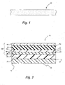
Figure 1 is a top view of an optical tape medium incorporating an embodiment of an imprint layer; -
Figure 2 is a cross sectional view of an optical tape medium incorporating an embodiment of an imprint layer; and -
Figure 3 is a schema illustration of a system for forming an optical tape medium. - Reference will now be made in detail to presently preferred compositions, embodiments and methods of the present invention, which constitute the best modes of practicing the invention presently known to the inventors. The Figures are not necessarily to scale. However, it is to be understood that the disclosed embodiments are merely exemplary of the invention that may be embodied in various and alternative forms. Therefore, specific details disclosed herein are not to be interpreted as limiting, but merely as a representative basis for any aspect of the invention and/or as a representative basis for teaching one skilled in the art to variously employ the present invention.
- Except in the examples, or where otherwise expressly indicated, all numerical quantities in this description indicating amounts of material or conditions of reaction and/or use are to be understood as modified by the word "about" in describing the broadest scope of the invention. Practice within the numerical limits stated is generally preferred. Also, unless expressly stated to the contrary: percent, "parts of," and ratio values are by weight; the description of a group or class of materials as suitable or preferred for a given purpose in connection with the invention implies that mixtures of any two or more of the members of the group or class are equally suitable or preferred; description of constituents in chemical terms refers to the constituents at the time of addition to any combination specified in the description, and does not necessarily preclude chemical interactions among the constituents of a mixture once mixed; the first definition of an acronym or other abbreviation applies to all subsequent uses herein of the same abbreviation; and, unless expressly stated to the contrary, measurement of a property is determined by the same technique as previously or later referenced for the same property.
- It is also to be understood that this invention is not limited to the specific embodiments and methods described below, as specific components and/or conditions may, of course, vary. Furthermore, the terminology used herein is used only for the purpose of describing particular embodiments of the present invention and is not intended to be limiting in any way.
- It must also be noted that, as used in the specification and the appended claims, the singular form "a," "an," and "the" comprise plural referents unless the context clearly indicates otherwise. For example, reference to a component in the singular is intended to comprise a plurality of components.
- Throughout this application, where publications are referenced, the disclosures of these publications in their entireties are hereby incorporated by reference into this application to more fully describe the state of the art to which this invention pertains.
- With reference to
Figures 1 and 2 , schematic illustrations of an optical tape medium for storing digital data are provided.Figure 1 is a top view of the optical tape medium.Figure 2 is a cross sectional view of the optical tape medium.Optical tape 10 includessubstrate film 12 havingsubstrate film sides substrate film 12 is formed from polyethylene naphthalate (PEN).Imprint layer 20 is disposed oversubstrate film side 16.Imprint layer 20 includesimprint layer side 22 andimprint layer side 24 withimprint layer side 22 being more proximate tosubstrate film 12. Advantageously,imprint layer 20 is made by the process set forth below. Multilayerdata recording assembly 28 is disposed overimprint layer 20. Multilayerdata recording assembly 28 typically includes one or more layers involved in the optical recording of data. - Still referring to
Figures 1 and 2 , an example of multilayerdata recording assembly 28 is provided. Multilayerdata recording assembly 28 includesmetal layer 30 disposed overimprint layer side 24.Metal layer 30 includesmetal layer side 32 andmetal layer side 34.Metal layer side 32 is more proximate toimprint layer 20 thanmetal layer side 34. Multilayerdata recording assembly 28 also includesdielectric layer 40 disposed overmetal layer side 34.Dielectric layer 40 includesdielectric layer side 42 anddielectric layer side 44 which is more proximate tometal layer 30. Multilayerdata recording assembly 28 further includesphase change layer 50 which is disposed overdielectric layer 40.Phase change layer 50 includes phasechange layer side 52 and phasechange layer side 54 which is more proximate tophase change layer 50. Finally, the present embodiment also includes multilayerdata recording assembly 28. Multilayerdata recording assembly 28 also includesdielectric layer 60 disposed overmetal layer side 54. - With reference to
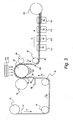
Figure 3 , a schematic diagram illustrating the fabrication of the optical storage medium set forth above is provided. Optical tape-forming system 70 includesspool 72 which suppliessubstrate film 16 which is of a tape-like configuration. During operation of optical tape-forming system 70,substrate film 12 moves in the directions indicated by d1-d5 and is guided by direction rollers 74-82.Substrate film side 16 ofsubstrate film 12 is coated with acurable liquid composition 86 fromdispenser 88. In a refinement,curable liquid composition 86 includes free radical photoinitiator and a polymerizable component that includes at least one acrylate. In the variation depicted inFigure 3 ,dispenser 88 is used to coatcurable liquid composition 86 ontosubstrate film 12. Coated substrate film 94 includescurable liquid layer 96 disposed onsubstrate film 12. Coated substrate film 94 proceeds to patterningroller 98. Patterningroller 98 includesprotrusions 100 that define the pattern to be imprinted upon coated substrate film 94. Curingenergy source 102 directs actinic radiation ontocurable liquid layer 96 to induce radical polymerization therein to formimprint layer 20. Typically, curingenergy source 102 is an ultraviolet ("UV") light source. Heatsource 104 is optionally present in order to provide heat to assist in the curing. After curing,imprint layer 20 haspattern 106 imprinted therein - Still referring to
Figure 3 , multilayerdata recording assembly 28 is fabricated along direction ds. In a variation,metal deposition station 110 is used to depositmetal layer 30 overimprint layer 20. Examples of deposition processes that may be used include sputtering and evaporation. Typically,metal deposition 110 is a sputtering reactor.Substrate film 12 proceeds next todielectric deposition station 112 to formdielectric layer 40.Phase change layer 50 is coated ontodielectric layer 40 at phasechange coating system 114. Typically,phase change layer 50 is a metal alloy, which has significant optical and electrical differences between the amorphous and crystalline states.Dielectric layer 60 is deposited ontophase change layer 50 viadielectric deposition station 116. It should be appreciated thatmetal layer 30, dielectric layers 40, 60 andphase change layer 50 can be single or multilayer structures. For example, some layers use two or three sub-layers to provide better reflection control and long term stability. Finally,optical tape 10 is rolled ontospool 120. Advantageously, the optical tape formed by the present method is observed to have superior mechanical and thermal properties. In particular, the method allows for the imprint layer to be formed with a thickness less than about 2 microns. In another refinement, the imprint layer has a thickness less than about 1.5 microns. In still another refinement, the imprint layer has a thickness greater than from about 0.1 to about 0.5 microns. In yet another variation, the imprint layer has a thickness greater than about 0.2 microns. In yet another variation, the imprint layer has a thickness between 0.3 and 0.4 microns. In still other variations, the imprint layer has a thickness from about 0.1 to about 0.25 microns. - In some variations, the optical tape processing is paused after formation of the imprint layer. In this variation, the coated substrate may be rolled onto a spool for later processing. In other variations, the optical tape may be subjected to a slitting process in order to fit in a cartridge.
- As set forth above, various embodiments of the present invention advantageously utilize a curable liquid composition that is radically polymerized. Advantageously, the curable, liquid composition has a viscosity less than about 50 cps at 25° C. In another refinement, the curable liquid composition has a viscosity less than about 30 cps at 25° C. In another refinement, the curable liquid composition has a viscosity less than about 20 cps at 25° C. In another refinement, the curable liquid composition has a viscosity less than about 10 cps at 25° C. Typically, the curable liquid composition has a viscosity greater than about 2 cps at 25° C. In another refinement, the curable liquid composition has a viscosity greater than about 5 cps at 25° C. The curable liquid composition includes one or more acrylates. Examples of suitable acrylates include monoacrylates, diacrylates, higher order functionality acrylates, and combinations thereof. In a refinement, the polymerizable comportent(s) are present in an amount from about 90 to about 99 weight percent of the total weight of the curable liquid composition. In another refinement, the polymerizable component(s) are present in an amount from about 93 to about 99 weight percent of the total weight of the curable liquid composition. In still another refinement, the polymerizable component(s) are present in an amount from about 95 to about 99 weight percent of the total weight of the curable liquid composition.
- In a variation, the curable liquid composition includes an acrylate having formula I:


- In a further refinement, the curable liquid composition also includes compounds having formula II:


- In a particularly useful variation, the curable liquid composition includes a combination of the compound having formula 1 and the acrylate having formula II. In a refinement of this variation, the acrylate having formula I is present in an amount from about 55 weight percent to about 75 weight percent of the total weight of the curable liquid composition and the acrylate having formula II is present in an amount from about 25 weight percent to about 45 weight percent of the total weight of the curable liquid composition.
- The curable liquid composition further includes a free radical photoinitiator. Suitable free radical photoinitiators include, but are not limited to, benzophenones, acetophenone derivatives, and combinations thereof. Specific examples include, alpha-hydroxyalkylphenylketones, benzoins (e.g., benzoin alkyl ethers and benzyl ketals), monoacylphosphine oxides, bisacylphosphine oxides, and combinations thereof. A particularly useful photoinitiator is Bis(2,4,6-trimethylbenzoyl)-phenylphosphineoxide. In a refinement, the free radical photoinitiatior is present in an amount from about 0.1 to about 10 weight percent of the total weight of the curable liquid composition. In another refinement, the free radical photoinitiatior is present in an amount from about 0.5 to about 8 weight percent of the total weight of the curable liquid composition. In still another refinement, the free radical photoinitiatior is present in an amount from about 1 to about 5 weight percent of the total weight of the curable liquid composition.
- The various methods of the present invention are used to form a polymeric imprint layer as set forth above. Therefore, the imprint layer is characterized by including residues of one or more of the acrylates set forth above. In particular, the imprint layer includes residues of the compounds describe by Formula I and II. The imprint layer also includes residues of the free radical photoinitiator(s)set forth above.
- A polymeric imprint layer is made by coating a mixture having about 66 weight percent Isobornyl acrylate, 30 weight percent 1,6-Hexanediol diacrylate, and 4 weight percent Bis(2,4,6-trimethylbenzoyl)-phenylphosphineoxide onto a substrate film. The coated substrate film to then cured with UV light while passing over a patterning roller to form the imprint layer.
- While embodiments of the invention have been illustrated and described, it is not intended that these embodiments illustrate and describe all possible forms of the invention. Rather, the words used in the specification are words of description rather than limitation, and it is understood that various changes may be made without departing from the spirit and scope of the invention.
- Further embodiments of the invention are defined in the following numbered clauses:
- 1. A method for forming an optical tape for data storage from a substrate film, the substrate film having a first substrate side and a second substrate side, the method comprising:
- a) patterning a curable liquid composition onto the second side of the substrate film, the curable liquid composition comprising a radical photoinitiator and a polymerizable component comprising at least one acrylate;
- b) illuminating the curable liquid composition to form a patterned imprint layer disposed over the substrate film, the imprint layer having a first imprint layer side and a second imprint layer side, the first imprint layer side being more proximate to the second substrate side than the second imprint layer side; and
- c) placing a multilayer data recording assembly over the second imprint layer side.
- 2. The method of clause 1 wherein the curable liquid composition includes an acrylate having formula I:

- 3. The method of clause 2 wherein R1 is hydrogen or methyl.
- 4. The method of clause 2 wherein R2 is n-butyl, t-butyl, isobornyl, phenyl, benzyl, dicylcopentenyl, dicyclopentenyl oxyethyl, ethylene glycol dicyclopentyl ether, cyclohexyl, and naphthyl.
- 5. The method of clause 1 wherein the curable liquid composition include a compound having the following formula:

- 6. The method of clause 1 wherein the curable liquid composition includes a compound having the following formula II:

- 7. The method of clause 3 wherein R3 is hydrogen or methyl.
- 8. The method of clause 3 wherein R4 is an alkylene group.
- 9. The method of clause 3 wherein R4 is described by -(CH2)n- and n is an integer from 1 to 10.
- 10. The method of cause 1 wherein the at least one acrylate has the following formule:

- 11. The method of clause 1 wherein step c) comprises
- d) depositing a metallic layer over the second imprint layer side;
- e) depositing a dielectric layer over the metallic layer;
- f) depositing a phase change layer over the first dielectric layer; and
- g) depositing a second dielectric-tajrer over the phase change layer.
- 12. The method of cause 1 wherein the curable liquid composition is illuminated with ultraviolet light.
- 13. The method of clause 1 wherein the curable liquid composition is patterned onto the second substrate side by:
- applying the curable liquid composition to the second substrate side to form a coated substrate; and
- contacting the curable liquid composition on the coated substrate with an imprinter such that a curable liquid composition is patterned.
- 14. A method for forming an optical tape for data storage from a substrate film, the substrate film having a first substrate side and a second substrate side, the method comprising:
- a) patterning a curable liquid composition onto the second side of the substrate film by:
- applying the curable liquid composition to the second substrate side to form a coated substrate; and
- contacting the curable liquid composition on the coated substrate with an
- imprinter such that a curable liquid composition is patterned;
the curable liquid composition including a free radical photoinitiator and a polymerizable component including a compound having formula I and a compounds having formula II:

- wherein:
- R1 is hydrogen or substituted or unsubstituted alkyl;
- R2 is a substituted or unsubstituted alkyl having more than 3 carbon atoms, cycloalkyl, cycloalkenyl, or substituted or unsubstituted aryl;
- R3 is hydrogen or substituted or unsubstituted alkyl; and
- R4 is a hydrocarbon moiety;
- b) illuminating the curable liquid composition to form a patterned imprint layer disposed over the substrate film, the imprint layer having a first imprint layer side and a second imprint layer side, the first imprint layer side being more proximate to the second substrate side than the second imprint layer side;
- c) placing a multilayer data recording assembly over the second imprint layer side;
- d) depositing a metallic layer over the second imprint layer side;
- e) depositing a dielectric layer over the metallic layer;
- f) depositing a phase change layer over the first dielectric layer; and
- g) depositing a second dielectric layer over the phase change layer.
- a) patterning a curable liquid composition onto the second side of the substrate film by:
- 15. The method of
clause 14 wherein the metallic layer is deposited by sputtering. - 16. The method of
clause 14 wherein:- R1 is hydrogen or methyl;
- R2 is Isobornyl, phenyl, benzyl, dicylcopentenyl, dicyclopentenyl oxyethyl, ethylene glycol dicyclopentyl ether, cyclohexyl, and naphthyl;
- R3 is hydrogen or methyl; and
- R4 is an alkylene group.
- 17. The method of
clause 14 wherein the curable liquid composition includes a compound having the following formula:
- 18. The method of clause 3 wherein R4 is described by -(CH2)n- and n is an integer from 1 to 10.
- 19. The method of clause 1 wherein the at least one acrylate has the following formula:

- 20. A polymeric imprint layer comprising residues of a free radical photoinitiator and a polymerizable component including a compound halving formula I and a compound having formula II:


- R1 is hydrogen or substituted or unsubstituted alkyl;
- R2 is a substituted or unsubstituted alkyl having more than 3 carbon atoms, cycloalkyl, cycloalkenyl, or substituted or unsubstituted aryl;
- R3 is hydrogen or substituted or unsubstituted alkyl; and
- R4 is a hydrocarbon moiety.
Claims (15)
- A method for forming an optical tape for data storage from a substrate film, the substrate film having a first substrate side and a second substrate side, the method comprising:a) patterning a curable liquid composition onto the second side of the substrate film, the curable liquid composition comprising a radical photoinitiator and a polymerizable component comprising at least one acrylate;b) illuminatirig the curable liquid composition to form a patterned imprint layer disposed over the substrate film, the imprint layer having a first imprint layer side and a second imprint layer side, the first imprint layer side being more proximate to the second substrate side than the second imprint layer side; andc) placing a multilayer data recording assembly over the second imprint layer side.
- The method of claim 1 wherein the curable liquid composition includes an acrylate having formula I:

- The method of claim 2 wherein R1 is hydrogen or methyl.
- The method of claim 2 wherein R2 is n-butyl, t-butyl, isobornyl, phenyl, benzyl, dicylcopentenyl, dicyclopentenyl oxyethyl, ethylene glycol dicyclopentyl ether, cyclohexyl, and naphthyl.
- The method of claim 1 wherein the curable liquid composition includes a compound having the following formula II:

- The method of claim 5 wherein R3 is hydrogen or Methyl.
- The method of claim 5 wherein R4 is an alkylene group.
- The method of claim 1 wherein step c) comprisesd) depositing a metallic layer over the second imprint layer side;e) depositing a dielectric layer over the metallic layer;f) depositing a phase change layer over the first dielectric layer; andg) depositing a second dielectric layer over the phase change layer.
- The method of claim 1 wherein the curable liquid composition is patterned onto the second substrate side by:applying the curable liquid composition to the second substrate side to form a coated substrate; andcontacting the curable liquid composition on the coated substrate with an imprinter such that a curable liquid composition is patterned.
- A method for forming an optical tape for data storage from a substrate film, the substrate film having a first substrate side and a second substrate side, the method comprising:a) patterning a curable liquid composition onto the second side of the substrate film by:applying the curable liquid composition to the second substrate side to form a coated substrate; andcontacting the curable liquid composition on the coated substrate with animprinter such that a curable liquid composition is patterned;
the curable liquid composition including a free radical photoinitiator and a polymerizable component including a compound having formula I and a compound having formula II:
 wherein:R1 is hydrogen or substituted or unsubstituted alkyl;- R2 is a substituted or unsubstituted alkyl having more than 3 carbon atoms, cycloalkyl, cycloaikenyl, or substituted or unsubstituted aryl;R3 is hydrogen or substituted or unsubstituted alkyl; andR4 is a hydrocarbon moiety;b) illuminating the curable liquid composition to form a patterned imprint layer disposed over the substrate film, the imprint layer having a frst imprint layer side and a second imprint layer side, the first imprint layer side being more proximate to the second substrate side than the second imprint layer side;c) placing a multilayer data recording assembly over the second imprint layer side;d) depositing a metallic layer over the second imprint layer side;e) depositing a dielectric layer over the metallic layer;f) depositing a phase change layer over the first dielectric layer; andg) depositing a second dielectric layer over the phase change layer.
 - The method of claim 10 wherein:R1 is hydrogen or methyl;R2 is isobornyl, phenyl, benzyl, dicylcopentenyl, dicyclopentenyl oxyethyl, ethylene glycol dicyclopentyl ether, cyclohexyl, and naphthyl;R3 is hydrogen or methyl; andR4 is an alkylene group.
- The method of claim 5 or 10 wherein the curable liquid composition includes a compound having the following formula:

- The method of claim 5 or 11 wherein R4 is described by -(CH2)n- and n is an integer from 1 to 10.
- The method of claim 1 our 10 wherein the at least one acrylate has the following formula:

- An optical tape for data storage comprising a substrate with a patterned polymeric imprint layer comprising residues of a free radical photoinitiator and a polymerizable component including a compound having formula I and a compound having formula II:

 R1 is hydrogen or substituted or unsubstituted alkyl;R2 is a substituted or unsubstituted alkyl having more than 3 carbon atoms, cycloalkyl, cycloalkenyl, or substituted or unsubstituted aryl;R3 is hydrogen or substituted or unsubstituted alkyl; andR4 is a hydrocarbon moiety.
Applications Claiming Priority (2)
| Application Number | Priority Date | Filing Date | Title |
|---|---|---|---|
| US12/822,592 US20110318534A1 (en) | 2010-06-24 | 2010-06-24 | Low Viscosity Monomer for Patterning Optical Tape |
| PCT/US2011/041737 WO2011163543A1 (en) | 2010-06-24 | 2011-06-24 | Low viscosity monomer for patterning optical tape |
Publications (2)
| Publication Number | Publication Date |
|---|---|
| EP2586027A1 EP2586027A1 (en) | 2013-05-01 |
| EP2586027B1 true EP2586027B1 (en) | 2015-07-22 |
Family
ID=44453889
Family Applications (1)
| Application Number | Title | Priority Date | Filing Date |
|---|---|---|---|
| EP11731590.3A Active EP2586027B1 (en) | 2010-06-24 | 2011-06-24 | Low viscosity monomers for patterning optical recording tapes |
Country Status (5)
| Country | Link |
|---|---|
| US (1) | US20110318534A1 (en) |
| EP (1) | EP2586027B1 (en) |
| JP (1) | JP5879341B2 (en) |
| CA (1) | CA2803281C (en) |
| WO (1) | WO2011163543A1 (en) |
Families Citing this family (2)
| Publication number | Priority date | Publication date | Assignee | Title |
|---|---|---|---|---|
| US9009745B2 (en) | 2012-11-15 | 2015-04-14 | Oracle International Corporation | Thin web optical media guiding method |
| US8869180B2 (en) * | 2012-11-27 | 2014-10-21 | Oracle America, Inc. | Rotary head multi-layer data storage and retrieval system and method |
Family Cites Families (8)
| Publication number | Priority date | Publication date | Assignee | Title |
|---|---|---|---|---|
| US4198446A (en) * | 1978-02-14 | 1980-04-15 | Ncr Corporation | Apparatus for the manufacture of a dual coated manifold sheet with pressure-rupturable materials |
| JP2708229B2 (en) * | 1989-05-31 | 1998-02-04 | ホーヤ株式会社 | Monomer composition for optical disk production |
| EP0519629A1 (en) * | 1991-06-11 | 1992-12-23 | Imperial Chemical Industries Plc | Recording media |
| US7106519B2 (en) * | 2003-07-31 | 2006-09-12 | Lucent Technologies Inc. | Tunable micro-lens arrays |
| JP2007287227A (en) * | 2006-04-14 | 2007-11-01 | Toshiba Corp | Write-once type information recording medium and disk unit |
| JP2008165845A (en) * | 2006-12-26 | 2008-07-17 | Hitachi Maxell Ltd | Tape-shaped optical recording medium, its manufacturing method and manufacturing device |
| JP2008198296A (en) * | 2007-02-14 | 2008-08-28 | Hitachi Maxell Ltd | Manufacturing method of servo pattern layer for information recording tape, its manufacture device, and information recording tape |
| JP2009032380A (en) * | 2007-03-05 | 2009-02-12 | Rohm & Haas Co | Curabile composition |
-
2010
- 2010-06-24 US US12/822,592 patent/US20110318534A1/en not_active Abandoned
-
2011
- 2011-06-24 WO PCT/US2011/041737 patent/WO2011163543A1/en active Application Filing
- 2011-06-24 JP JP2013516787A patent/JP5879341B2/en active Active
- 2011-06-24 EP EP11731590.3A patent/EP2586027B1/en active Active
- 2011-06-24 CA CA2803281A patent/CA2803281C/en active Active
Also Published As
| Publication number | Publication date |
|---|---|
| WO2011163543A1 (en) | 2011-12-29 |
| JP5879341B2 (en) | 2016-03-08 |
| JP2013529826A (en) | 2013-07-22 |
| EP2586027A1 (en) | 2013-05-01 |
| CA2803281A1 (en) | 2011-12-29 |
| US20110318534A1 (en) | 2011-12-29 |
| CA2803281C (en) | 2019-04-30 |
Similar Documents
| Publication | Publication Date | Title |
|---|---|---|
| KR100926858B1 (en) | Method of producing optical disk-use original and method of producing optical disk | |
| KR20040089444A (en) | Resist Material and Microfabrication Method | |
| US7741006B2 (en) | Laser patterning method for fabricating disc stamper | |
| KR20120031908A (en) | Method for producing curable composition for imprints | |
| EP2586027B1 (en) | Low viscosity monomers for patterning optical recording tapes | |
| DE69503835T2 (en) | Photopolymerizable compositions containing thioethers | |
| CN101427312B (en) | Ultraviolet-curable composition for optical disk and optical disk | |
| JP3879726B2 (en) | Manufacturing method of optical disc master and manufacturing method of optical disc | |
| WO2002023544A1 (en) | Optical recording medium | |
| JP2002092957A (en) | Material of surface protecting layer for optical recording medium | |
| JP4534417B2 (en) | Manufacturing method of sputter target | |
| US20110318506A1 (en) | Optical Tape Media Patterning Using Cationic Polymerizable Monomers | |
| JP2009117513A (en) | Photosetting or thermosetting type resin composition for nanoimprinting having resistance to dry etching | |
| JPS60121442A (en) | Photosensitive record memory medium and recording/ reproducing method | |
| CN100582936C (en) | Resist material and nanofabrication method | |
| US20120306124A1 (en) | UV Curing of Embossed Structures | |
| TW200903480A (en) | Ultraviolet-curing composition for optical disk and optical disk | |
| CN103262165B (en) | Form the compositions of hard disk tunicle | |
| CN104011797B (en) | Optical medium with transparent backsides coating | |
| JP2008226287A (en) | Stamper for optical disk and its manufacturing method | |
| US20070259150A1 (en) | Optical storage medium | |
| US5164290A (en) | Optical recording medium | |
| KR20140068201A (en) | Flattening film forming composition for hard disk | |
| CN100595832C (en) | Optical information recording medium and manufacturing method of optical information recording medium | |
| JP2007317347A (en) | Optical storage medium |
Legal Events
| Date | Code | Title | Description |
|---|---|---|---|
| PUAI | Public reference made under article 153(3) epc to a published international application that has entered the european phase |
Free format text: ORIGINAL CODE: 0009012 |
|
| 17P | Request for examination filed |
Effective date: 20130114 |
|
| AK | Designated contracting states |
Kind code of ref document: A1 Designated state(s): AL AT BE BG CH CY CZ DE DK EE ES FI FR GB GR HR HU IE IS IT LI LT LU LV MC MK MT NL NO PL PT RO RS SE SI SK SM TR |
|
| DAX | Request for extension of the european patent (deleted) | ||
| 17Q | First examination report despatched |
Effective date: 20140206 |
|
| GRAP | Despatch of communication of intention to grant a patent |
Free format text: ORIGINAL CODE: EPIDOSNIGR1 |
|
| INTG | Intention to grant announced |
Effective date: 20140930 |
|
| GRAP | Despatch of communication of intention to grant a patent |
Free format text: ORIGINAL CODE: EPIDOSNIGR1 |
|
| INTG | Intention to grant announced |
Effective date: 20150205 |
|
| GRAS | Grant fee paid |
Free format text: ORIGINAL CODE: EPIDOSNIGR3 |
|
| GRAA | (expected) grant |
Free format text: ORIGINAL CODE: 0009210 |
|
| AK | Designated contracting states |
Kind code of ref document: B1 Designated state(s): AL AT BE BG CH CY CZ DE DK EE ES FI FR GB GR HR HU IE IS IT LI LT LU LV MC MK MT NL NO PL PT RO RS SE SI SK SM TR |
|
| REG | Reference to a national code |
Ref country code: GB Ref legal event code: FG4D |
|
| REG | Reference to a national code |
Ref country code: CH Ref legal event code: EP |
|
| REG | Reference to a national code |
Ref country code: IE Ref legal event code: FG4D |
|
| REG | Reference to a national code |
Ref country code: AT Ref legal event code: REF Ref document number: 738297 Country of ref document: AT Kind code of ref document: T Effective date: 20150815 |
|
| REG | Reference to a national code |
Ref country code: DE Ref legal event code: R096 Ref document number: 602011018036 Country of ref document: DE |
|
| REG | Reference to a national code |
Ref country code: AT Ref legal event code: MK05 Ref document number: 738297 Country of ref document: AT Kind code of ref document: T Effective date: 20150722 |
|
| REG | Reference to a national code |
Ref country code: LT Ref legal event code: MG4D |
|
| REG | Reference to a national code |
Ref country code: NL Ref legal event code: MP Effective date: 20150722 |
|
| PG25 | Lapsed in a contracting state [announced via postgrant information from national office to epo] |
Ref country code: LV Free format text: LAPSE BECAUSE OF FAILURE TO SUBMIT A TRANSLATION OF THE DESCRIPTION OR TO PAY THE FEE WITHIN THE PRESCRIBED TIME-LIMIT Effective date: 20150722 Ref country code: FI Free format text: LAPSE BECAUSE OF FAILURE TO SUBMIT A TRANSLATION OF THE DESCRIPTION OR TO PAY THE FEE WITHIN THE PRESCRIBED TIME-LIMIT Effective date: 20150722 Ref country code: LT Free format text: LAPSE BECAUSE OF FAILURE TO SUBMIT A TRANSLATION OF THE DESCRIPTION OR TO PAY THE FEE WITHIN THE PRESCRIBED TIME-LIMIT Effective date: 20150722 Ref country code: NO Free format text: LAPSE BECAUSE OF FAILURE TO SUBMIT A TRANSLATION OF THE DESCRIPTION OR TO PAY THE FEE WITHIN THE PRESCRIBED TIME-LIMIT Effective date: 20151022 Ref country code: GR Free format text: LAPSE BECAUSE OF FAILURE TO SUBMIT A TRANSLATION OF THE DESCRIPTION OR TO PAY THE FEE WITHIN THE PRESCRIBED TIME-LIMIT Effective date: 20151023 |
|
| PG25 | Lapsed in a contracting state [announced via postgrant information from national office to epo] |
Ref country code: PT Free format text: LAPSE BECAUSE OF FAILURE TO SUBMIT A TRANSLATION OF THE DESCRIPTION OR TO PAY THE FEE WITHIN THE PRESCRIBED TIME-LIMIT Effective date: 20151123 Ref country code: ES Free format text: LAPSE BECAUSE OF FAILURE TO SUBMIT A TRANSLATION OF THE DESCRIPTION OR TO PAY THE FEE WITHIN THE PRESCRIBED TIME-LIMIT Effective date: 20150722 Ref country code: SE Free format text: LAPSE BECAUSE OF FAILURE TO SUBMIT A TRANSLATION OF THE DESCRIPTION OR TO PAY THE FEE WITHIN THE PRESCRIBED TIME-LIMIT Effective date: 20150722 Ref country code: IS Free format text: LAPSE BECAUSE OF FAILURE TO SUBMIT A TRANSLATION OF THE DESCRIPTION OR TO PAY THE FEE WITHIN THE PRESCRIBED TIME-LIMIT Effective date: 20151122 Ref country code: AT Free format text: LAPSE BECAUSE OF FAILURE TO SUBMIT A TRANSLATION OF THE DESCRIPTION OR TO PAY THE FEE WITHIN THE PRESCRIBED TIME-LIMIT Effective date: 20150722 Ref country code: RS Free format text: LAPSE BECAUSE OF FAILURE TO SUBMIT A TRANSLATION OF THE DESCRIPTION OR TO PAY THE FEE WITHIN THE PRESCRIBED TIME-LIMIT Effective date: 20150722 Ref country code: HR Free format text: LAPSE BECAUSE OF FAILURE TO SUBMIT A TRANSLATION OF THE DESCRIPTION OR TO PAY THE FEE WITHIN THE PRESCRIBED TIME-LIMIT Effective date: 20150722 Ref country code: PL Free format text: LAPSE BECAUSE OF FAILURE TO SUBMIT A TRANSLATION OF THE DESCRIPTION OR TO PAY THE FEE WITHIN THE PRESCRIBED TIME-LIMIT Effective date: 20150722 |
|
| REG | Reference to a national code |
Ref country code: DE Ref legal event code: R097 Ref document number: 602011018036 Country of ref document: DE |
|
| PG25 | Lapsed in a contracting state [announced via postgrant information from national office to epo] |
Ref country code: IT Free format text: LAPSE BECAUSE OF FAILURE TO SUBMIT A TRANSLATION OF THE DESCRIPTION OR TO PAY THE FEE WITHIN THE PRESCRIBED TIME-LIMIT Effective date: 20150722 Ref country code: CZ Free format text: LAPSE BECAUSE OF FAILURE TO SUBMIT A TRANSLATION OF THE DESCRIPTION OR TO PAY THE FEE WITHIN THE PRESCRIBED TIME-LIMIT Effective date: 20150722 Ref country code: SK Free format text: LAPSE BECAUSE OF FAILURE TO SUBMIT A TRANSLATION OF THE DESCRIPTION OR TO PAY THE FEE WITHIN THE PRESCRIBED TIME-LIMIT Effective date: 20150722 Ref country code: DK Free format text: LAPSE BECAUSE OF FAILURE TO SUBMIT A TRANSLATION OF THE DESCRIPTION OR TO PAY THE FEE WITHIN THE PRESCRIBED TIME-LIMIT Effective date: 20150722 Ref country code: EE Free format text: LAPSE BECAUSE OF FAILURE TO SUBMIT A TRANSLATION OF THE DESCRIPTION OR TO PAY THE FEE WITHIN THE PRESCRIBED TIME-LIMIT Effective date: 20150722 |
|
| PLBE | No opposition filed within time limit |
Free format text: ORIGINAL CODE: 0009261 |
|
| STAA | Information on the status of an ep patent application or granted ep patent |
Free format text: STATUS: NO OPPOSITION FILED WITHIN TIME LIMIT |
|
| PG25 | Lapsed in a contracting state [announced via postgrant information from national office to epo] |
Ref country code: RO Free format text: LAPSE BECAUSE OF FAILURE TO SUBMIT A TRANSLATION OF THE DESCRIPTION OR TO PAY THE FEE WITHIN THE PRESCRIBED TIME-LIMIT Effective date: 20150722 |
|
| 26N | No opposition filed |
Effective date: 20160425 |
|
| PG25 | Lapsed in a contracting state [announced via postgrant information from national office to epo] |
Ref country code: SI Free format text: LAPSE BECAUSE OF FAILURE TO SUBMIT A TRANSLATION OF THE DESCRIPTION OR TO PAY THE FEE WITHIN THE PRESCRIBED TIME-LIMIT Effective date: 20150722 |
|
| PG25 | Lapsed in a contracting state [announced via postgrant information from national office to epo] |
Ref country code: BE Free format text: LAPSE BECAUSE OF FAILURE TO SUBMIT A TRANSLATION OF THE DESCRIPTION OR TO PAY THE FEE WITHIN THE PRESCRIBED TIME-LIMIT Effective date: 20150722 |
|
| PG25 | Lapsed in a contracting state [announced via postgrant information from national office to epo] |
Ref country code: MC Free format text: LAPSE BECAUSE OF FAILURE TO SUBMIT A TRANSLATION OF THE DESCRIPTION OR TO PAY THE FEE WITHIN THE PRESCRIBED TIME-LIMIT Effective date: 20150722 |
|
| REG | Reference to a national code |
Ref country code: IE Ref legal event code: MM4A |
|
| REG | Reference to a national code |
Ref country code: FR Ref legal event code: ST Effective date: 20170228 |
|
| PG25 | Lapsed in a contracting state [announced via postgrant information from national office to epo] |
Ref country code: FR Free format text: LAPSE BECAUSE OF NON-PAYMENT OF DUE FEES Effective date: 20160630 |
|
| PG25 | Lapsed in a contracting state [announced via postgrant information from national office to epo] |
Ref country code: IE Free format text: LAPSE BECAUSE OF NON-PAYMENT OF DUE FEES Effective date: 20160624 |
|
| PG25 | Lapsed in a contracting state [announced via postgrant information from national office to epo] |
Ref country code: NL Free format text: LAPSE BECAUSE OF FAILURE TO SUBMIT A TRANSLATION OF THE DESCRIPTION OR TO PAY THE FEE WITHIN THE PRESCRIBED TIME-LIMIT Effective date: 20150722 |
|
| PG25 | Lapsed in a contracting state [announced via postgrant information from national office to epo] |
Ref country code: CY Free format text: LAPSE BECAUSE OF FAILURE TO SUBMIT A TRANSLATION OF THE DESCRIPTION OR TO PAY THE FEE WITHIN THE PRESCRIBED TIME-LIMIT Effective date: 20150722 Ref country code: SM Free format text: LAPSE BECAUSE OF FAILURE TO SUBMIT A TRANSLATION OF THE DESCRIPTION OR TO PAY THE FEE WITHIN THE PRESCRIBED TIME-LIMIT Effective date: 20150722 Ref country code: HU Free format text: LAPSE BECAUSE OF FAILURE TO SUBMIT A TRANSLATION OF THE DESCRIPTION OR TO PAY THE FEE WITHIN THE PRESCRIBED TIME-LIMIT; INVALID AB INITIO Effective date: 20110624 |
|
| PG25 | Lapsed in a contracting state [announced via postgrant information from national office to epo] |
Ref country code: TR Free format text: LAPSE BECAUSE OF FAILURE TO SUBMIT A TRANSLATION OF THE DESCRIPTION OR TO PAY THE FEE WITHIN THE PRESCRIBED TIME-LIMIT Effective date: 20150722 Ref country code: LU Free format text: LAPSE BECAUSE OF NON-PAYMENT OF DUE FEES Effective date: 20160624 Ref country code: MT Free format text: LAPSE BECAUSE OF NON-PAYMENT OF DUE FEES Effective date: 20160630 Ref country code: MK Free format text: LAPSE BECAUSE OF FAILURE TO SUBMIT A TRANSLATION OF THE DESCRIPTION OR TO PAY THE FEE WITHIN THE PRESCRIBED TIME-LIMIT Effective date: 20150722 |
|
| PG25 | Lapsed in a contracting state [announced via postgrant information from national office to epo] |
Ref country code: BG Free format text: LAPSE BECAUSE OF FAILURE TO SUBMIT A TRANSLATION OF THE DESCRIPTION OR TO PAY THE FEE WITHIN THE PRESCRIBED TIME-LIMIT Effective date: 20150722 |
|
| PG25 | Lapsed in a contracting state [announced via postgrant information from national office to epo] |
Ref country code: AL Free format text: LAPSE BECAUSE OF FAILURE TO SUBMIT A TRANSLATION OF THE DESCRIPTION OR TO PAY THE FEE WITHIN THE PRESCRIBED TIME-LIMIT Effective date: 20150722 |
|
| REG | Reference to a national code |
Ref country code: DE Ref legal event code: R082 Ref document number: 602011018036 Country of ref document: DE Representative=s name: D YOUNG & CO LLP, DE |
|
| P01 | Opt-out of the competence of the unified patent court (upc) registered |
Effective date: 20230522 |
|
| PGFP | Annual fee paid to national office [announced via postgrant information from national office to epo] |
Ref country code: CH Payment date: 20230702 Year of fee payment: 13 |
|
| PGFP | Annual fee paid to national office [announced via postgrant information from national office to epo] |
Ref country code: GB Payment date: 20240502 Year of fee payment: 14 |
|
| PGFP | Annual fee paid to national office [announced via postgrant information from national office to epo] |
Ref country code: DE Payment date: 20240502 Year of fee payment: 14 |