EP2579317A1 - Method of manufacturing a solar cell with local back contacts - Google Patents
Method of manufacturing a solar cell with local back contacts Download PDFInfo
- Publication number
- EP2579317A1 EP2579317A1 EP11290466.9A EP11290466A EP2579317A1 EP 2579317 A1 EP2579317 A1 EP 2579317A1 EP 11290466 A EP11290466 A EP 11290466A EP 2579317 A1 EP2579317 A1 EP 2579317A1
- Authority
- EP
- European Patent Office
- Prior art keywords
- dielectric layer
- dielectric
- manufacturing
- layer
- manufacturing according
- Prior art date
- Legal status (The legal status is an assumption and is not a legal conclusion. Google has not performed a legal analysis and makes no representation as to the accuracy of the status listed.)
- Withdrawn
Links
Images
Classifications
-
- H—ELECTRICITY
- H10—SEMICONDUCTOR DEVICES; ELECTRIC SOLID-STATE DEVICES NOT OTHERWISE PROVIDED FOR
- H10F—INORGANIC SEMICONDUCTOR DEVICES SENSITIVE TO INFRARED RADIATION, LIGHT, ELECTROMAGNETIC RADIATION OF SHORTER WAVELENGTH OR CORPUSCULAR RADIATION
- H10F77/00—Constructional details of devices covered by this subclass
- H10F77/20—Electrodes
- H10F77/206—Electrodes for devices having potential barriers
- H10F77/211—Electrodes for devices having potential barriers for photovoltaic cells
- H10F77/219—Arrangements for electrodes of back-contact photovoltaic cells
-
- B—PERFORMING OPERATIONS; TRANSPORTING
- B23—MACHINE TOOLS; METAL-WORKING NOT OTHERWISE PROVIDED FOR
- B23K—SOLDERING OR UNSOLDERING; WELDING; CLADDING OR PLATING BY SOLDERING OR WELDING; CUTTING BY APPLYING HEAT LOCALLY, e.g. FLAME CUTTING; WORKING BY LASER BEAM
- B23K26/00—Working by laser beam, e.g. welding, cutting or boring
- B23K26/36—Removing material
- B23K26/361—Removing material for deburring or mechanical trimming
-
- B—PERFORMING OPERATIONS; TRANSPORTING
- B23—MACHINE TOOLS; METAL-WORKING NOT OTHERWISE PROVIDED FOR
- B23K—SOLDERING OR UNSOLDERING; WELDING; CLADDING OR PLATING BY SOLDERING OR WELDING; CUTTING BY APPLYING HEAT LOCALLY, e.g. FLAME CUTTING; WORKING BY LASER BEAM
- B23K26/00—Working by laser beam, e.g. welding, cutting or boring
- B23K26/36—Removing material
- B23K26/362—Laser etching
-
- B—PERFORMING OPERATIONS; TRANSPORTING
- B23—MACHINE TOOLS; METAL-WORKING NOT OTHERWISE PROVIDED FOR
- B23K—SOLDERING OR UNSOLDERING; WELDING; CLADDING OR PLATING BY SOLDERING OR WELDING; CUTTING BY APPLYING HEAT LOCALLY, e.g. FLAME CUTTING; WORKING BY LASER BEAM
- B23K26/00—Working by laser beam, e.g. welding, cutting or boring
- B23K26/36—Removing material
- B23K26/40—Removing material taking account of the properties of the material involved
-
- H—ELECTRICITY
- H10—SEMICONDUCTOR DEVICES; ELECTRIC SOLID-STATE DEVICES NOT OTHERWISE PROVIDED FOR
- H10F—INORGANIC SEMICONDUCTOR DEVICES SENSITIVE TO INFRARED RADIATION, LIGHT, ELECTROMAGNETIC RADIATION OF SHORTER WAVELENGTH OR CORPUSCULAR RADIATION
- H10F10/00—Individual photovoltaic cells, e.g. solar cells
- H10F10/10—Individual photovoltaic cells, e.g. solar cells having potential barriers
- H10F10/11—Photovoltaic cells having point contact potential barriers
-
- H—ELECTRICITY
- H10—SEMICONDUCTOR DEVICES; ELECTRIC SOLID-STATE DEVICES NOT OTHERWISE PROVIDED FOR
- H10F—INORGANIC SEMICONDUCTOR DEVICES SENSITIVE TO INFRARED RADIATION, LIGHT, ELECTROMAGNETIC RADIATION OF SHORTER WAVELENGTH OR CORPUSCULAR RADIATION
- H10F71/00—Manufacture or treatment of devices covered by this subclass
-
- H—ELECTRICITY
- H10—SEMICONDUCTOR DEVICES; ELECTRIC SOLID-STATE DEVICES NOT OTHERWISE PROVIDED FOR
- H10F—INORGANIC SEMICONDUCTOR DEVICES SENSITIVE TO INFRARED RADIATION, LIGHT, ELECTROMAGNETIC RADIATION OF SHORTER WAVELENGTH OR CORPUSCULAR RADIATION
- H10F71/00—Manufacture or treatment of devices covered by this subclass
- H10F71/121—The active layers comprising only Group IV materials
-
- H—ELECTRICITY
- H10—SEMICONDUCTOR DEVICES; ELECTRIC SOLID-STATE DEVICES NOT OTHERWISE PROVIDED FOR
- H10F—INORGANIC SEMICONDUCTOR DEVICES SENSITIVE TO INFRARED RADIATION, LIGHT, ELECTROMAGNETIC RADIATION OF SHORTER WAVELENGTH OR CORPUSCULAR RADIATION
- H10F77/00—Constructional details of devices covered by this subclass
- H10F77/20—Electrodes
- H10F77/206—Electrodes for devices having potential barriers
- H10F77/211—Electrodes for devices having potential barriers for photovoltaic cells
-
- H—ELECTRICITY
- H10—SEMICONDUCTOR DEVICES; ELECTRIC SOLID-STATE DEVICES NOT OTHERWISE PROVIDED FOR
- H10F—INORGANIC SEMICONDUCTOR DEVICES SENSITIVE TO INFRARED RADIATION, LIGHT, ELECTROMAGNETIC RADIATION OF SHORTER WAVELENGTH OR CORPUSCULAR RADIATION
- H10F77/00—Constructional details of devices covered by this subclass
- H10F77/30—Coatings
- H10F77/306—Coatings for devices having potential barriers
- H10F77/311—Coatings for devices having potential barriers for photovoltaic cells
- H10F77/315—Coatings for devices having potential barriers for photovoltaic cells the coatings being antireflective or having enhancing optical properties
-
- B—PERFORMING OPERATIONS; TRANSPORTING
- B23—MACHINE TOOLS; METAL-WORKING NOT OTHERWISE PROVIDED FOR
- B23K—SOLDERING OR UNSOLDERING; WELDING; CLADDING OR PLATING BY SOLDERING OR WELDING; CUTTING BY APPLYING HEAT LOCALLY, e.g. FLAME CUTTING; WORKING BY LASER BEAM
- B23K2103/00—Materials to be soldered, welded or cut
- B23K2103/16—Composite materials
- B23K2103/166—Multilayered materials
- B23K2103/172—Multilayered materials wherein at least one of the layers is non-metallic
-
- Y—GENERAL TAGGING OF NEW TECHNOLOGICAL DEVELOPMENTS; GENERAL TAGGING OF CROSS-SECTIONAL TECHNOLOGIES SPANNING OVER SEVERAL SECTIONS OF THE IPC; TECHNICAL SUBJECTS COVERED BY FORMER USPC CROSS-REFERENCE ART COLLECTIONS [XRACs] AND DIGESTS
- Y02—TECHNOLOGIES OR APPLICATIONS FOR MITIGATION OR ADAPTATION AGAINST CLIMATE CHANGE
- Y02E—REDUCTION OF GREENHOUSE GAS [GHG] EMISSIONS, RELATED TO ENERGY GENERATION, TRANSMISSION OR DISTRIBUTION
- Y02E10/00—Energy generation through renewable energy sources
- Y02E10/50—Photovoltaic [PV] energy
- Y02E10/547—Monocrystalline silicon PV cells
-
- Y—GENERAL TAGGING OF NEW TECHNOLOGICAL DEVELOPMENTS; GENERAL TAGGING OF CROSS-SECTIONAL TECHNOLOGIES SPANNING OVER SEVERAL SECTIONS OF THE IPC; TECHNICAL SUBJECTS COVERED BY FORMER USPC CROSS-REFERENCE ART COLLECTIONS [XRACs] AND DIGESTS
- Y02—TECHNOLOGIES OR APPLICATIONS FOR MITIGATION OR ADAPTATION AGAINST CLIMATE CHANGE
- Y02P—CLIMATE CHANGE MITIGATION TECHNOLOGIES IN THE PRODUCTION OR PROCESSING OF GOODS
- Y02P70/00—Climate change mitigation technologies in the production process for final industrial or consumer products
- Y02P70/50—Manufacturing or production processes characterised by the final manufactured product
Definitions
- the invention relates to a method of manufacturing a solar cell with local back contacts.
- the method of this invention can be applied for several manufacturing designs, such as PERC (passivated emiller and rear ccll), PERL ( passivated emitter and rear locally-diffused) or IBC (Interdigitated Back Contact) type solar cells.
- PERC passivated emiller and rear ccll
- PERL passivated emitter and rear locally-diffused
- IBC Interdigitated Back Contact
- the back face of the solar cells comprises a reflective coating made of a dielectric layer and a metal layer.
- the dielectric layer provides the aforementioned passivation. This dielectric layer is opened locally in order to allow the contact between the bulk silicon and the metal layer deposited right after.
- the most commonly used dielectric layer is hydrogenated silicon nitride (SiNx: H).
- This layer shows intrinsically net positive charges, which create a parasitic emitter layer for the case of p-type substrates, also called inversion layer, which, after the creation of a metallic contact, is responsible for an increase in recombination.
- the standard passivation stack for the back side is made of silicon oxide (SiO2) and SiNx: H, in order to decrease this effect.
- AlOx aluminium oxide
- the present invention aims at mitigating, at least partially, the drawbacks described above.
- the invention proposes a method of manufacturing a solar cell with local back contacts comprising a dielectric stack of at least two layers presenting at least a first dielectric layer of AlOx or SiOx in contact with a layer of p-type silicon and a second dielectric layer deposited on the first dielectric layer, characterized in that it comprises a step of formation of at least one partial opening in the dielectric stack, leaving at least partially the aforementioned first dielectric layer at the location of the partial opening.
- the damages caused by the laser beam such as the local heating and the delamination, occur only in the second dielectric layer, the first dielectric layer being at least partially preserved and the underlying bulk silicon is totally preserved.
- the dielectric layers have passivation propertiesA good passivation quality is thus maintained around the openings, which contributes to an improvement in short-circuit current and (Jsc), open circuit voltage (Voc), and in particular in the output compared to cells where the dielectric layer is completely ablated.
- diagrams represent three steps (a), (b) and (c) of the manufacturing method of a solar cell with passivated back surface and local back contacts according to the invention.
- Figure 1 example consists of a PERC type solar cell ( passivaled emitter and rear cell).
- the photovoltaic cell 1 comprises a layer 3 substrate or p-type silicon wafer, a layer 5 of n-doped silicon on the front face 7.
- an anti-reflecting layer 9 for example, silicon nitride SiNx.
- the first dielectric layer 11 is aluminum oxide AlOx. According to another example this dielectric layer is made of SiOx.
- the second dielectric layer 13 is for example silicon nitride SiNx, in particular hydrogenated silicon nitride SINx: H. In other cases also, for example, SiOx can be used, or combination of both, or any other suitable stack.
- the first dielectric layer 11 is in contact with substrate 3 and the second dielectric layer 13 is deposited on the first dielectric layer 11.
- step (b) one can proceed with a formation step of at least one local opening 15 by laser ablation in passivation. stack 10, leaving at least partially the aforementioned first dielectric layer 11.
- step (b) one can proceed with a formation step of at least one local opening 15 by laser ablation in passivation. stack 10, leaving at least partially the aforementioned first dielectric layer 11.
- optimal laser conditions i.e. pulse duration, wavelength, power, etc
- pulse duration, wavelength, power, etc allowing a partial ablation as described above
- the first dielectric layer 11 preferably has a layer thickness thick enough (at least 1 nm) to exhibit negative charges and thin enough to allow a low temperature diffusion of A1 metal through AlOx to form the contact, for example a thickness of at least a few monolayers after ablation, meaning a thick ness between 1 nm and 30 nm after ablation.
- the silicon of substrate 3 is not damaged by laser ablation.
- any pattern suitable for good optical reflection properties and with optimal metalized contacted area For example, one can use a pattern composed of partial openings of about 40 ⁇ m separated by 600 ⁇ m.
- the damages caused by the laser beam such as for example the local heating and the delamination occur only on the level of the second dielectric layer 13, the first dielectric layer 11 being preserved.
- step (c) one proceeds to a step of a metallization layer 17 application on the rear face 19 of the photovoltaic cell.
- a metallization layer 17 application on the rear face 19 of the photovoltaic cell.
- Any Al-based metallization method can be applied. This can for example be carried out by Al-sputtering on the rear face 19 of the solar cell 1.
- step (d) one performs on the areas where at least one partial opening 15 is spared, a backsurface field (BSF) formation by firing in a furnace at a temperature T>740°C, for example at 815°C.
- BSF backsurface field
- Figure 3 shows the manufacturing process of a solar cell similar to that on figure 1 , but this time for a PERL type solar cell.
- p+ doped zones 21 were created beforehand as local BSF, for example with B diffusion. Apart from this, steps (a) to (c) are similar.
- the metallization step (c) one carries out an annealing step for the formation of the metal contacts on the back side region 19, for example at 400°C. In this case also, an increase in the performances of the cell was also observed.
Landscapes
- Engineering & Computer Science (AREA)
- Physics & Mathematics (AREA)
- Optics & Photonics (AREA)
- Plasma & Fusion (AREA)
- Mechanical Engineering (AREA)
- Photovoltaic Devices (AREA)
- Life Sciences & Earth Sciences (AREA)
- Sustainable Development (AREA)
- Sustainable Energy (AREA)
- Manufacturing & Machinery (AREA)
Abstract
The invention relates to the manufacturing process of a solar cell (1) with back contact and passivated emitter, comprising a dielectric stack (10) of at least two layers consisting of at least a first dielectric layer (11) made of AlOx or SiOx in contact with a p-type silicon layer (3), and a second dielectric layer (13) deposited on the first dielectric layer (11). Besides, the method of manufacturing comprising a formation step of at least one partial opening (15) preferably by laser ablation into the dielectric stack (10), sparing at least partially the aforementioned first dielectric layer.
Description
- The invention relates to a method of manufacturing a solar cell with local back contacts.
- The method of this invention can be applied for several manufacturing designs, such as PERC (passivated emiller and rear ccll), PERL (passivated emitter and rear locally-diffused) or IBC (Interdigitated Back Contact) type solar cells.
- For all of them, good passivation properties on the back face of the wafer surface are mandatory in order to reduce recombination losses.
- In PERC technology, for example, the back face of the solar cells comprises a reflective coating made of a dielectric layer and a metal layer. The dielectric layer provides the aforementioned passivation. This dielectric layer is opened locally in order to allow the contact between the bulk silicon and the metal layer deposited right after.
- In silicon solar cells, the most commonly used dielectric layer is hydrogenated silicon nitride (SiNx: H). This layer shows intrinsically net positive charges, which create a parasitic emitter layer for the case of p-type substrates, also called inversion layer, which, after the creation of a metallic contact, is responsible for an increase in recombination.
- Thus, in p-Lype silicon PERC solar cells, the standard passivation stack for the back side is made of silicon oxide (SiO2) and SiNx: H, in order to decrease this effect.
- Recently, works have been reported on the use of aluminium oxide (AlOx) layers for passivating the back side of p-type silicon solar cells. These AlOx layers have been shown to have intrinsic negative charges, which prevent the creation of a parasitic emitter on p-type silicon and facilitate the field-effect passivation.
- In addition, a common way to fabricate the local openings into the dielectric layers is by means of laser ablation, which goes completely through the passivation stack.
- However, it was shown that laser ablation of the SiO2 and SiNx passivation layers melts the underlying silicon surface, inducing damages. Various types of laser-induced damages can be created such as delamination or cracks in the dielectric layers around the openings, melting of the silicon, overheating of the dielectric layers around the openings. These damages induce a decrease in the passivation performance.
- Moreover, it was shown that the damages caused in AlOx/SiNx passivation layers could modify the charges in the AlOx layer, thus inducing a decrease in field-effect passivation and leading to the creation of a parasitic emitter layer detrimental to solar cell performance.
- The present invention aims at mitigating, at least partially, the drawbacks described above.
- For this purpose, the invention proposes a method of manufacturing a solar cell with local back contacts comprising a dielectric stack of at least two layers presenting at least a first dielectric layer of AlOx or SiOx in contact with a layer of p-type silicon and a second dielectric layer deposited on the first dielectric layer, characterized in that it comprises a step of formation of at least one partial opening in the dielectric stack, leaving at least partially the aforementioned first dielectric layer at the location of the partial opening.
- Thanks to this process, the damages caused by the laser beam, such as the local heating and the delamination, occur only in the second dielectric layer, the first dielectric layer being at least partially preserved and the underlying bulk silicon is totally preserved.
- In addition, the dielectric layers have passivation propertiesA good passivation quality is thus maintained around the openings, which contributes to an improvement in short-circuit current and (Jsc), open circuit voltage (Voc), and in particular in the output compared to cells where the dielectric layer is completely ablated.
- According to other characteristics taken alone or in combination:
- the step of formation of at least one partial opening in the dielectric stack comprises a laser ablation step,
- the ablation step is carried out using a pulse laser which pulse duration is less than a few nanoseconds,
- the first dielectric layer exhibits negative charges allowing field effect passivation,
- the first dielectric layer has a thickness of at least a few monolayers after ablation,
- the second dielectric layer is made of SiNx,.
- the ablation step is carried out using a laser which radiates in the UV region, more specifically around 355nm.
- Other advantages and characteristics will appear with the reading of the description of the following figures, among which:
-
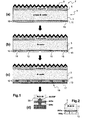
figure 1 shows diagrams of manufacturing of a PERC type solar cell. -
figure 2 shows a detail at the rear side after partial ablation of the dielectric stack. -
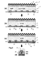
figure 3 shows diagrams of manufacturing of a PERI. type solar cell. - On all the figures the same references refer to the same elements.
- On
figure 1 , diagrams represent three steps (a), (b) and (c) of the manufacturing method of a solar cell with passivated back surface and local back contacts according to the invention. -
Figure 1 example, consists of a PERC type solar cell (passivaled emitter and rear cell). - Of course, these three steps do not represent the whole cell manufacturing method, but only the steps concerning the invention. The other manufacturing steps are known by the field specialists, and do not require a description within the framework of this invention.
- As can be seen on
figure 1(a) , at this step of manufacture, thephotovoltaic cell 1 comprises alayer 3 substrate or p-type silicon wafer, alayer 5 of n-doped silicon on thefront face 7. - On the
front face 7 is also deposited an anti-reflecting layer 9 (ARC for "antireflection coating"), for example, silicon nitride SiNx. - On the back face of
cell 1 is deposited astack 10 of at least twodielectric layers - In the present example, the first
dielectric layer 11 is aluminum oxide AlOx. According to another example this dielectric layer is made of SiOx. - The second
dielectric layer 13 is for example silicon nitride SiNx, in particular hydrogenated silicon nitride SINx: H. In other cases also, for example, SiOx can be used, or combination of both, or any other suitable stack. - The first
dielectric layer 11 is in contact withsubstrate 3 and the seconddielectric layer 13 is deposited on the firstdielectric layer 11. - According to step (b), one can proceed with a formation step of at least one
local opening 15 by laser ablation in passivation.stack 10, leaving at least partially the aforementioned firstdielectric layer 11. One thus can obtain the configuration shown according to a detail onfigure 2 . - For this ablation process, optimal laser conditions (i.e. pulse duration, wavelength, power, etc) allowing a partial ablation as described above can be determined experimentally and are specific to the dielectric stack to be ablated. For example, one can use a single pulse laser of less than a few nanoseconds, also picoseconds or femptoseconds pulses and in the UV range, in particular at 355nm wavelength.
- After ablation, the first
dielectric layer 11 preferably has a layer thickness thick enough (at least 1 nm) to exhibit negative charges and thin enough to allow a low temperature diffusion of A1 metal through AlOx to form the contact, for example a thickness of at least a few monolayers after ablation, meaning a thick ness between 1 nm and 30 nm after ablation. - Thus, the silicon of
substrate 3 is not damaged by laser ablation. - Typically, one carries out the aforementioned partial openings by laser ablation with any pattern suitable for good optical reflection properties and with optimal metalized contacted area. For example, one can use a pattern composed of partial openings of about 40 µm separated by 600µm.
- Thanks to this process, the damages caused by the laser beam such as for example the local heating and the delamination occur only on the level of the second
dielectric layer 13, the firstdielectric layer 11 being preserved. - Then, on step (c), one proceeds to a step of a
metallization layer 17 application on therear face 19 of the photovoltaic cell. Any Al-based metallization method can be applied. This can for example be carried out by Al-sputtering on therear face 19 of thesolar cell 1. - Finally, on step (d), one performs on the areas where at least one
partial opening 15 is spared, a backsurface field (BSF) formation by firing in a furnace at a temperature T>740°C, for example at 815°C. - Thanks to the method according to the invention, a good passivation quality around the metal contacts is maintained, which contributes to an improvement of the values of short circuit current (Jsc) by 1.6% and of open circuit voltage (Voc) by 1.156 compared experimentally with solar cells manufactured according to state of the art processes where the passivation stack is completely ablated. Similarly, the fill factor FF is improved by 0.35% and the efficiency itself by approximately 3%.
-
Figure 3 shows the manufacturing process of a solar cell similar to that onfigure 1 , but this time for a PERL type solar cell. - In this case and unlike PERC cells, in the regions of metal contacts to be fabricated, p+ doped
zones 21 were created beforehand as local BSF, for example with B diffusion. Apart from this, steps (a) to (c) are similar. - Then, after the metallization step (c), one carries out an annealing step for the formation of the metal contacts on the
back side region 19, for example at 400°C. In this case also, an increase in the performances of the cell was also observed.
Claims (7)
- Method of manufacturing a solar cell with local back contacts (1) comprising a dielectric stack (10) of at least two layers presenting at least a first dielectric layer of AlOx or SiOx (11) in contact with a layer (3) of p-type silicon and a second dielectric layer (13) deposited on the first dielectric layer (11), characterized in that it comprises a step of formation of at least one partial opening (15) in the dielectric stack (10), leaving at least partially the aforementioned first dielectric layer (11) at the location of the partial opening.
- Method of manufacturing according to claim 1, wherein the step of formation of at least one partial opening (15) in the dielectric stack (10) comprises a laser ablation step.
- Method of manufacturing according to claim 2, wherein the ablation step is carried out using a pulse laser which pulse duration is less than a few nanoseconds.
- Method of manufacturing according to any of the claims 1 to 3, wherein the first dielectric layer (11) exhibits negative charges allowing field effect passivation.
- Method of manufacturing according to any of the claims 1 to 4, wherein the first dielectric layer (11) has a thickness of at least a few monolayers after ablation.
- Method of manufacturing according to any of the claims 1 to 5, wherein the second dielectric layer (13) is made of SiNx.
- Method of manufacturing according to any of the claims 2 to 6, wherein the ablation step is carried out using a laser which radiates in the UV region, more specifically around 355nm.
Priority Applications (7)
| Application Number | Priority Date | Filing Date | Title |
|---|---|---|---|
| EP11290466.9A EP2579317A1 (en) | 2011-10-07 | 2011-10-07 | Method of manufacturing a solar cell with local back contacts |
| CN201280049697.0A CN104247033B (en) | 2011-10-07 | 2012-10-05 | Method of manufacturing solar cells with localized back contacts |
| EP12768863.8A EP2764553B1 (en) | 2011-10-07 | 2012-10-05 | Method of manufacturing a solar cell with local back contacts |
| PCT/EP2012/069764 WO2013050556A1 (en) | 2011-10-07 | 2012-10-05 | Method of manufacturing a solar cell with local back contacts |
| US14/349,111 US9722106B2 (en) | 2011-10-07 | 2012-10-05 | Method of manufacturing a solar cell with local back contacts |
| JP2014533926A JP2014531778A (en) | 2011-10-07 | 2012-10-05 | Method for manufacturing solar cell with local back contact |
| JP2018197111A JP2019050385A (en) | 2011-10-07 | 2018-10-19 | Method of manufacturing a solar cell having a local back contact |
Applications Claiming Priority (1)
| Application Number | Priority Date | Filing Date | Title |
|---|---|---|---|
| EP11290466.9A EP2579317A1 (en) | 2011-10-07 | 2011-10-07 | Method of manufacturing a solar cell with local back contacts |
Publications (1)
| Publication Number | Publication Date |
|---|---|
| EP2579317A1 true EP2579317A1 (en) | 2013-04-10 |
Family
ID=46970343
Family Applications (2)
| Application Number | Title | Priority Date | Filing Date |
|---|---|---|---|
| EP11290466.9A Withdrawn EP2579317A1 (en) | 2011-10-07 | 2011-10-07 | Method of manufacturing a solar cell with local back contacts |
| EP12768863.8A Active EP2764553B1 (en) | 2011-10-07 | 2012-10-05 | Method of manufacturing a solar cell with local back contacts |
Family Applications After (1)
| Application Number | Title | Priority Date | Filing Date |
|---|---|---|---|
| EP12768863.8A Active EP2764553B1 (en) | 2011-10-07 | 2012-10-05 | Method of manufacturing a solar cell with local back contacts |
Country Status (5)
| Country | Link |
|---|---|
| US (1) | US9722106B2 (en) |
| EP (2) | EP2579317A1 (en) |
| JP (2) | JP2014531778A (en) |
| CN (1) | CN104247033B (en) |
| WO (1) | WO2013050556A1 (en) |
Cited By (3)
| Publication number | Priority date | Publication date | Assignee | Title |
|---|---|---|---|---|
| JP2016058438A (en) * | 2014-09-05 | 2016-04-21 | 日立化成株式会社 | Passivation layer protective layer forming composition, solar cell element, method for producing the same, and solar cell |
| CN105940503A (en) * | 2013-12-02 | 2016-09-14 | 索莱克赛尔公司 | Passivated contacts for back contact back junction solar cells |
| CN110299418A (en) * | 2014-01-29 | 2019-10-01 | Lg电子株式会社 | Solar battery and its manufacturing method |
Families Citing this family (15)
| Publication number | Priority date | Publication date | Assignee | Title |
|---|---|---|---|---|
| US9929294B2 (en) * | 2012-05-14 | 2018-03-27 | Mitsubishi Electric Corporation | Photoelectric conversion device, manufacturing method thereof, and photoelectric conversion module |
| CN103594564B (en) * | 2013-12-03 | 2016-03-02 | 常州天合光能有限公司 | The manufacture method of all back-contact electrodes solar cell and all back-contact electrodes solar cell |
| KR101614190B1 (en) * | 2013-12-24 | 2016-04-20 | 엘지전자 주식회사 | Solar cell and manufacturing method thereof |
| CN104465885B (en) * | 2014-12-23 | 2017-01-25 | 常州天合光能有限公司 | Production method for achieving local metallization of all-back-contact electrode solar cell |
| TWI573284B (en) * | 2015-03-26 | 2017-03-01 | 茂迪股份有限公司 | Solar cell, module comprising the same, and method of manufacturing the same |
| CN105470349A (en) * | 2015-12-30 | 2016-04-06 | 无锡赛晶太阳能有限公司 | PERC solar cell and preparation method thereof |
| CN105470337A (en) * | 2015-12-30 | 2016-04-06 | 无锡赛晶太阳能有限公司 | PERC solar cell and preparation method thereof |
| CN105845775A (en) * | 2016-04-19 | 2016-08-10 | 晋能清洁能源科技有限公司 | Back multilayer coating method of PERC crystalline silicon solar cell |
| CN106784033A (en) * | 2016-12-13 | 2017-05-31 | 广东爱康太阳能科技有限公司 | A kind of crystal silicon solar energy battery and preparation method thereof |
| CN107068790A (en) * | 2017-03-03 | 2017-08-18 | 广东爱康太阳能科技有限公司 | Preparation method, battery, component and the system of p-type PERC solar cells |
| TWI705573B (en) * | 2019-07-05 | 2020-09-21 | 太極能源科技股份有限公司 | Solar cell having rear stacked back passivation layer and method for manufacturing the same |
| CN113707755A (en) * | 2020-05-22 | 2021-11-26 | 一道新能源科技(衢州)有限公司 | IBC crystalline silicon solar cell and manufacturing method thereof |
| CN114038921B (en) | 2021-11-05 | 2024-03-29 | 晶科能源(海宁)有限公司 | Solar cell and photovoltaic module |
| CN116851940A (en) * | 2022-03-28 | 2023-10-10 | 山东浪潮华光光电子股份有限公司 | A new method of opening holes in passivation layer |
| CN115207156A (en) * | 2022-06-27 | 2022-10-18 | 常州时创能源股份有限公司 | A kind of preparation method of P-type IBC battery |
Family Cites Families (5)
| Publication number | Priority date | Publication date | Assignee | Title |
|---|---|---|---|---|
| US7575999B2 (en) * | 2004-09-01 | 2009-08-18 | Micron Technology, Inc. | Method for creating conductive elements for semiconductor device structures using laser ablation processes and methods of fabricating semiconductor device assemblies |
| FR2906403B1 (en) * | 2006-09-21 | 2008-12-19 | Commissariat Energie Atomique | METHOD FOR RECLAIMING PHOTOVOLTAIC CELLS |
| US8324015B2 (en) * | 2009-12-01 | 2012-12-04 | Sunpower Corporation | Solar cell contact formation using laser ablation |
| US20120024336A1 (en) * | 2010-07-27 | 2012-02-02 | Jeong-Mo Hwang | Charge control of solar cell passivation layers |
| CN102064232A (en) * | 2010-10-28 | 2011-05-18 | 中山大学 | Process applied to single-surface corroded p-n junction or suede structure of crystalline silicon solar cell |
-
2011
- 2011-10-07 EP EP11290466.9A patent/EP2579317A1/en not_active Withdrawn
-
2012
- 2012-10-05 JP JP2014533926A patent/JP2014531778A/en active Pending
- 2012-10-05 US US14/349,111 patent/US9722106B2/en active Active
- 2012-10-05 EP EP12768863.8A patent/EP2764553B1/en active Active
- 2012-10-05 WO PCT/EP2012/069764 patent/WO2013050556A1/en not_active Ceased
- 2012-10-05 CN CN201280049697.0A patent/CN104247033B/en not_active Expired - Fee Related
-
2018
- 2018-10-19 JP JP2018197111A patent/JP2019050385A/en active Pending
Non-Patent Citations (6)
| Title |
|---|
| ANNEROSE KNORZ ET AL: "Selective laser ablation of SiN x layers on textured surfaces for low temperature front side metallizations", PROGRESS IN PHOTOVOLTAICS: RESEARCH AND APPLICATIONS, vol. 17, no. 2, 1 March 2009 (2009-03-01), pages 127 - 136, XP055021042, ISSN: 1062-7995, DOI: 10.1002/pip.856 * |
| DIMITRI ZIELKE ET AL: "Contact passivation in silicon solar cells using atomic-layer-deposited aluminum oxide layers", PHYSICA STATUS SOLIDI (RRL) - RAPID RESEARCH LETTERS, vol. 5, no. 8, 1 August 2011 (2011-08-01), pages 298 - 300, XP055021093, ISSN: 1862-6254, DOI: 10.1002/pssr.201105285 * |
| GERRIT HEINRICH ET AL: "Investigation of ablation mechanisms for selective laser ablation of silicon nitride layers", ENERGY PROCEDIA, vol. 8, 17 April 2011 (2011-04-17) - 20 April 2011 (2011-04-20), pages 592 - 597, XP007920356 * |
| JAFFRENNOU P ET AL: "Laser Ablation of SiO2/SiNx and AlOx/SiNx Back Side Passivation Stacks for Advanced Cell Architectures", 26TH EUROPEAN PHOTOVOLTAIC SOLAR ENERGY CONFERENCE AND EXHIBITION, 5 September 2011 (2011-09-05) - 9 September 2011 (2011-09-09), pages 2180 - 2183, XP007920354, ISBN: 3-936338-27-2, DOI: 10.4229/26THEUPVSEC2011-2CV4.4.14 * |
| M. BÄHR ET AL: "Ablation of Dielectrics without Substrate Damage Using Ultra-Short-Pulse Laser Systems", PROCEEDINGS OF THE 25TH EUROPEAN PHOTOVOLTAIC SOLAR ENERGY CONFERENCE, 6 September 2010 (2010-09-06) - 10 September 2010 (2010-09-10), pages 2490 - 2496, XP040531262, ISBN: 978-3-936338-26-3 * |
| PENAUD J ET AL: "Integration of AlOx Passivation Layer in PERC-Based Solar Cells", 26TH EUROPEAN PHOTOVOLTAIC SOLAR ENERGY CONFERENCE AND EXHIBITION,, 5 September 2011 (2011-09-05) - 9 September 2011 (2011-09-09), pages 2243 - 2246, XP007920355, ISBN: 3-936338-27-2, DOI: 10.4229/26THEUPVSEC2011-2CV.4.38 * |
Cited By (3)
| Publication number | Priority date | Publication date | Assignee | Title |
|---|---|---|---|---|
| CN105940503A (en) * | 2013-12-02 | 2016-09-14 | 索莱克赛尔公司 | Passivated contacts for back contact back junction solar cells |
| CN110299418A (en) * | 2014-01-29 | 2019-10-01 | Lg电子株式会社 | Solar battery and its manufacturing method |
| JP2016058438A (en) * | 2014-09-05 | 2016-04-21 | 日立化成株式会社 | Passivation layer protective layer forming composition, solar cell element, method for producing the same, and solar cell |
Also Published As
| Publication number | Publication date |
|---|---|
| EP2764553B1 (en) | 2019-07-24 |
| US20140311563A1 (en) | 2014-10-23 |
| JP2014531778A (en) | 2014-11-27 |
| JP2019050385A (en) | 2019-03-28 |
| WO2013050556A1 (en) | 2013-04-11 |
| EP2764553A1 (en) | 2014-08-13 |
| CN104247033B (en) | 2016-12-07 |
| CN104247033A (en) | 2014-12-24 |
| US9722106B2 (en) | 2017-08-01 |
Similar Documents
| Publication | Publication Date | Title |
|---|---|---|
| EP2764553B1 (en) | Method of manufacturing a solar cell with local back contacts | |
| Röder et al. | Add‐on laser tailored selective emitter solar cells | |
| JP6633709B2 (en) | Manufacturing method and structure of solar cell | |
| Metz et al. | Industrial high performance crystalline silicon solar cells and modules based on rear surface passivation technology | |
| EP2239788A1 (en) | Solar battery element and solar battery element manufacturing method | |
| CN114038922B (en) | A back-contact heterojunction solar cell with improved insulation performance and its fabrication method | |
| EP2740157B1 (en) | Interdigitated electrode formation | |
| US20150017747A1 (en) | Method for forming a solar cell with a selective emitter | |
| CN104810416A (en) | Solar cell and manufacturing method thereof | |
| CN111466033A (en) | Thin film solar modules with improved shunt resistance | |
| KR101396027B1 (en) | Ion implantation and annealing for high efficiency back-contact back-junction solar cells | |
| KR101954436B1 (en) | Method for forming metal silicide layers | |
| EP2362425A1 (en) | A method for forming a selective contact | |
| Tao et al. | 20.7% efficient ion‐implanted large area n‐type front junction silicon solar cells with rear point contacts formed by laser opening and physical vapor deposition | |
| TW200826310A (en) | Thin-film solar module | |
| JP5375414B2 (en) | Solar cell and manufacturing method thereof | |
| US8828790B2 (en) | Method for local contacting and local doping of a semiconductor layer | |
| CN111886698A (en) | Method for producing a thin-film solar module | |
| EP2645427A1 (en) | Extended laser ablation in solar cell manufacture | |
| Jäger et al. | Laser doping for high-efficiency silicon solar cells | |
| JP2001267613A (en) | Integrated thin-film solar cell and method of manufacturing the same | |
| Bay et al. | Benefits of different process routes for industrial direct front side plating | |
| Cho et al. | Effect of Rear Passivation and Local Back Contact for High Efficiency c-Si Solar Cell with Variable Laser Feed Speed | |
| EP4336569A1 (en) | Photovoltaic cell with double-sided passive contacts and comprising tco portions localized under the front metallization | |
| Janušonis et al. | Electroless copper contacts for low concentration silicon solar cells |
Legal Events
| Date | Code | Title | Description |
|---|---|---|---|
| PUAI | Public reference made under article 153(3) epc to a published international application that has entered the european phase |
Free format text: ORIGINAL CODE: 0009012 |
|
| AK | Designated contracting states |
Kind code of ref document: A1 Designated state(s): AL AT BE BG CH CY CZ DE DK EE ES FI FR GB GR HR HU IE IS IT LI LT LU LV MC MK MT NL NO PL PT RO RS SE SI SK SM TR |
|
| AX | Request for extension of the european patent |
Extension state: BA ME |
|
| STAA | Information on the status of an ep patent application or granted ep patent |
Free format text: STATUS: THE APPLICATION IS DEEMED TO BE WITHDRAWN |
|
| 18D | Application deemed to be withdrawn |
Effective date: 20131011 |