EP2575220A2 - Laser accordable avec référence de longueur d'onde intégrée - Google Patents
Laser accordable avec référence de longueur d'onde intégrée Download PDFInfo
- Publication number
- EP2575220A2 EP2575220A2 EP12006832A EP12006832A EP2575220A2 EP 2575220 A2 EP2575220 A2 EP 2575220A2 EP 12006832 A EP12006832 A EP 12006832A EP 12006832 A EP12006832 A EP 12006832A EP 2575220 A2 EP2575220 A2 EP 2575220A2
- Authority
- EP
- European Patent Office
- Prior art keywords
- wavelength
- tunable laser
- tunable
- silicon
- region
- Prior art date
- Legal status (The legal status is an assumption and is not a legal conclusion. Google has not performed a legal analysis and makes no representation as to the accuracy of the status listed.)
- Granted
Links
Images


Classifications
-
- H—ELECTRICITY
- H01—ELECTRIC ELEMENTS
- H01S—DEVICES USING THE PROCESS OF LIGHT AMPLIFICATION BY STIMULATED EMISSION OF RADIATION [LASER] TO AMPLIFY OR GENERATE LIGHT; DEVICES USING STIMULATED EMISSION OF ELECTROMAGNETIC RADIATION IN WAVE RANGES OTHER THAN OPTICAL
- H01S5/00—Semiconductor lasers
- H01S5/06—Arrangements for controlling the laser output parameters, e.g. by operating on the active medium
- H01S5/068—Stabilisation of laser output parameters
-
- H—ELECTRICITY
- H01—ELECTRIC ELEMENTS
- H01S—DEVICES USING THE PROCESS OF LIGHT AMPLIFICATION BY STIMULATED EMISSION OF RADIATION [LASER] TO AMPLIFY OR GENERATE LIGHT; DEVICES USING STIMULATED EMISSION OF ELECTROMAGNETIC RADIATION IN WAVE RANGES OTHER THAN OPTICAL
- H01S5/00—Semiconductor lasers
- H01S5/02—Structural details or components not essential to laser action
- H01S5/026—Monolithically integrated components, e.g. waveguides, monitoring photo-detectors, drivers
-
- H—ELECTRICITY
- H01—ELECTRIC ELEMENTS
- H01S—DEVICES USING THE PROCESS OF LIGHT AMPLIFICATION BY STIMULATED EMISSION OF RADIATION [LASER] TO AMPLIFY OR GENERATE LIGHT; DEVICES USING STIMULATED EMISSION OF ELECTROMAGNETIC RADIATION IN WAVE RANGES OTHER THAN OPTICAL
- H01S3/00—Lasers, i.e. devices using stimulated emission of electromagnetic radiation in the infrared, visible or ultraviolet wave range
- H01S3/0014—Monitoring arrangements not otherwise provided for
-
- H—ELECTRICITY
- H01—ELECTRIC ELEMENTS
- H01S—DEVICES USING THE PROCESS OF LIGHT AMPLIFICATION BY STIMULATED EMISSION OF RADIATION [LASER] TO AMPLIFY OR GENERATE LIGHT; DEVICES USING STIMULATED EMISSION OF ELECTROMAGNETIC RADIATION IN WAVE RANGES OTHER THAN OPTICAL
- H01S3/00—Lasers, i.e. devices using stimulated emission of electromagnetic radiation in the infrared, visible or ultraviolet wave range
- H01S3/05—Construction or shape of optical resonators; Accommodation of active medium therein; Shape of active medium
- H01S3/06—Construction or shape of active medium
- H01S3/063—Waveguide lasers, i.e. whereby the dimensions of the waveguide are of the order of the light wavelength
- H01S3/0632—Thin film lasers in which light propagates in the plane of the thin film
- H01S3/0637—Integrated lateral waveguide, e.g. the active waveguide is integrated on a substrate made by Si on insulator technology (Si/SiO2)
-
- H—ELECTRICITY
- H01—ELECTRIC ELEMENTS
- H01S—DEVICES USING THE PROCESS OF LIGHT AMPLIFICATION BY STIMULATED EMISSION OF RADIATION [LASER] TO AMPLIFY OR GENERATE LIGHT; DEVICES USING STIMULATED EMISSION OF ELECTROMAGNETIC RADIATION IN WAVE RANGES OTHER THAN OPTICAL
- H01S3/00—Lasers, i.e. devices using stimulated emission of electromagnetic radiation in the infrared, visible or ultraviolet wave range
- H01S3/05—Construction or shape of optical resonators; Accommodation of active medium therein; Shape of active medium
- H01S3/06—Construction or shape of active medium
- H01S3/063—Waveguide lasers, i.e. whereby the dimensions of the waveguide are of the order of the light wavelength
- H01S3/067—Fibre lasers
- H01S3/0675—Resonators including a grating structure, e.g. distributed Bragg reflectors [DBR] or distributed feedback [DFB] fibre lasers
-
- H—ELECTRICITY
- H01—ELECTRIC ELEMENTS
- H01S—DEVICES USING THE PROCESS OF LIGHT AMPLIFICATION BY STIMULATED EMISSION OF RADIATION [LASER] TO AMPLIFY OR GENERATE LIGHT; DEVICES USING STIMULATED EMISSION OF ELECTROMAGNETIC RADIATION IN WAVE RANGES OTHER THAN OPTICAL
- H01S3/00—Lasers, i.e. devices using stimulated emission of electromagnetic radiation in the infrared, visible or ultraviolet wave range
- H01S3/10—Controlling the intensity, frequency, phase, polarisation or direction of the emitted radiation, e.g. switching, gating, modulating or demodulating
- H01S3/10007—Controlling the intensity, frequency, phase, polarisation or direction of the emitted radiation, e.g. switching, gating, modulating or demodulating in optical amplifiers
- H01S3/10015—Controlling the intensity, frequency, phase, polarisation or direction of the emitted radiation, e.g. switching, gating, modulating or demodulating in optical amplifiers by monitoring or controlling, e.g. attenuating, the input signal
-
- H—ELECTRICITY
- H01—ELECTRIC ELEMENTS
- H01S—DEVICES USING THE PROCESS OF LIGHT AMPLIFICATION BY STIMULATED EMISSION OF RADIATION [LASER] TO AMPLIFY OR GENERATE LIGHT; DEVICES USING STIMULATED EMISSION OF ELECTROMAGNETIC RADIATION IN WAVE RANGES OTHER THAN OPTICAL
- H01S3/00—Lasers, i.e. devices using stimulated emission of electromagnetic radiation in the infrared, visible or ultraviolet wave range
- H01S3/10—Controlling the intensity, frequency, phase, polarisation or direction of the emitted radiation, e.g. switching, gating, modulating or demodulating
- H01S3/10007—Controlling the intensity, frequency, phase, polarisation or direction of the emitted radiation, e.g. switching, gating, modulating or demodulating in optical amplifiers
- H01S3/10023—Controlling the intensity, frequency, phase, polarisation or direction of the emitted radiation, e.g. switching, gating, modulating or demodulating in optical amplifiers by functional association of additional optical elements, e.g. filters, gratings, reflectors
-
- H—ELECTRICITY
- H01—ELECTRIC ELEMENTS
- H01S—DEVICES USING THE PROCESS OF LIGHT AMPLIFICATION BY STIMULATED EMISSION OF RADIATION [LASER] TO AMPLIFY OR GENERATE LIGHT; DEVICES USING STIMULATED EMISSION OF ELECTROMAGNETIC RADIATION IN WAVE RANGES OTHER THAN OPTICAL
- H01S3/00—Lasers, i.e. devices using stimulated emission of electromagnetic radiation in the infrared, visible or ultraviolet wave range
- H01S3/10—Controlling the intensity, frequency, phase, polarisation or direction of the emitted radiation, e.g. switching, gating, modulating or demodulating
- H01S3/10007—Controlling the intensity, frequency, phase, polarisation or direction of the emitted radiation, e.g. switching, gating, modulating or demodulating in optical amplifiers
- H01S3/10023—Controlling the intensity, frequency, phase, polarisation or direction of the emitted radiation, e.g. switching, gating, modulating or demodulating in optical amplifiers by functional association of additional optical elements, e.g. filters, gratings, reflectors
- H01S3/1003—Controlling the intensity, frequency, phase, polarisation or direction of the emitted radiation, e.g. switching, gating, modulating or demodulating in optical amplifiers by functional association of additional optical elements, e.g. filters, gratings, reflectors tunable optical elements, e.g. acousto-optic filters, tunable gratings
-
- H—ELECTRICITY
- H01—ELECTRIC ELEMENTS
- H01S—DEVICES USING THE PROCESS OF LIGHT AMPLIFICATION BY STIMULATED EMISSION OF RADIATION [LASER] TO AMPLIFY OR GENERATE LIGHT; DEVICES USING STIMULATED EMISSION OF ELECTROMAGNETIC RADIATION IN WAVE RANGES OTHER THAN OPTICAL
- H01S3/00—Lasers, i.e. devices using stimulated emission of electromagnetic radiation in the infrared, visible or ultraviolet wave range
- H01S3/10—Controlling the intensity, frequency, phase, polarisation or direction of the emitted radiation, e.g. switching, gating, modulating or demodulating
- H01S3/105—Controlling the intensity, frequency, phase, polarisation or direction of the emitted radiation, e.g. switching, gating, modulating or demodulating by controlling the mutual position or the reflecting properties of the reflectors of the cavity, e.g. by controlling the cavity length
- H01S3/1055—Controlling the intensity, frequency, phase, polarisation or direction of the emitted radiation, e.g. switching, gating, modulating or demodulating by controlling the mutual position or the reflecting properties of the reflectors of the cavity, e.g. by controlling the cavity length one of the reflectors being constituted by a diffraction grating
-
- H—ELECTRICITY
- H01—ELECTRIC ELEMENTS
- H01S—DEVICES USING THE PROCESS OF LIGHT AMPLIFICATION BY STIMULATED EMISSION OF RADIATION [LASER] TO AMPLIFY OR GENERATE LIGHT; DEVICES USING STIMULATED EMISSION OF ELECTROMAGNETIC RADIATION IN WAVE RANGES OTHER THAN OPTICAL
- H01S3/00—Lasers, i.e. devices using stimulated emission of electromagnetic radiation in the infrared, visible or ultraviolet wave range
- H01S3/10—Controlling the intensity, frequency, phase, polarisation or direction of the emitted radiation, e.g. switching, gating, modulating or demodulating
- H01S3/13—Stabilisation of laser output parameters, e.g. frequency or amplitude
- H01S3/1305—Feedback control systems
-
- H—ELECTRICITY
- H01—ELECTRIC ELEMENTS
- H01S—DEVICES USING THE PROCESS OF LIGHT AMPLIFICATION BY STIMULATED EMISSION OF RADIATION [LASER] TO AMPLIFY OR GENERATE LIGHT; DEVICES USING STIMULATED EMISSION OF ELECTROMAGNETIC RADIATION IN WAVE RANGES OTHER THAN OPTICAL
- H01S5/00—Semiconductor lasers
- H01S5/02—Structural details or components not essential to laser action
- H01S5/0206—Substrates, e.g. growth, shape, material, removal or bonding
- H01S5/021—Silicon based substrates
-
- H—ELECTRICITY
- H01—ELECTRIC ELEMENTS
- H01S—DEVICES USING THE PROCESS OF LIGHT AMPLIFICATION BY STIMULATED EMISSION OF RADIATION [LASER] TO AMPLIFY OR GENERATE LIGHT; DEVICES USING STIMULATED EMISSION OF ELECTROMAGNETIC RADIATION IN WAVE RANGES OTHER THAN OPTICAL
- H01S5/00—Semiconductor lasers
- H01S5/02—Structural details or components not essential to laser action
- H01S5/024—Arrangements for thermal management
- H01S5/02453—Heating, e.g. the laser is heated for stabilisation against temperature fluctuations of the environment
-
- H—ELECTRICITY
- H01—ELECTRIC ELEMENTS
- H01S—DEVICES USING THE PROCESS OF LIGHT AMPLIFICATION BY STIMULATED EMISSION OF RADIATION [LASER] TO AMPLIFY OR GENERATE LIGHT; DEVICES USING STIMULATED EMISSION OF ELECTROMAGNETIC RADIATION IN WAVE RANGES OTHER THAN OPTICAL
- H01S5/00—Semiconductor lasers
- H01S5/06—Arrangements for controlling the laser output parameters, e.g. by operating on the active medium
- H01S5/0607—Arrangements for controlling the laser output parameters, e.g. by operating on the active medium by varying physical parameters other than the potential of the electrodes, e.g. by an electric or magnetic field, mechanical deformation, pressure, light, temperature
- H01S5/0612—Arrangements for controlling the laser output parameters, e.g. by operating on the active medium by varying physical parameters other than the potential of the electrodes, e.g. by an electric or magnetic field, mechanical deformation, pressure, light, temperature controlled by temperature
-
- H—ELECTRICITY
- H01—ELECTRIC ELEMENTS
- H01S—DEVICES USING THE PROCESS OF LIGHT AMPLIFICATION BY STIMULATED EMISSION OF RADIATION [LASER] TO AMPLIFY OR GENERATE LIGHT; DEVICES USING STIMULATED EMISSION OF ELECTROMAGNETIC RADIATION IN WAVE RANGES OTHER THAN OPTICAL
- H01S5/00—Semiconductor lasers
- H01S5/10—Construction or shape of the optical resonator, e.g. extended or external cavity, coupled cavities, bent-guide, varying width, thickness or composition of the active region
- H01S5/1028—Coupling to elements in the cavity, e.g. coupling to waveguides adjacent the active region, e.g. forward coupled [DFC] structures
-
- H—ELECTRICITY
- H01—ELECTRIC ELEMENTS
- H01S—DEVICES USING THE PROCESS OF LIGHT AMPLIFICATION BY STIMULATED EMISSION OF RADIATION [LASER] TO AMPLIFY OR GENERATE LIGHT; DEVICES USING STIMULATED EMISSION OF ELECTROMAGNETIC RADIATION IN WAVE RANGES OTHER THAN OPTICAL
- H01S5/00—Semiconductor lasers
- H01S5/10—Construction or shape of the optical resonator, e.g. extended or external cavity, coupled cavities, bent-guide, varying width, thickness or composition of the active region
- H01S5/12—Construction or shape of the optical resonator, e.g. extended or external cavity, coupled cavities, bent-guide, varying width, thickness or composition of the active region the resonator having a periodic structure, e.g. in distributed feedback [DFB] lasers
- H01S5/1206—Construction or shape of the optical resonator, e.g. extended or external cavity, coupled cavities, bent-guide, varying width, thickness or composition of the active region the resonator having a periodic structure, e.g. in distributed feedback [DFB] lasers having a non constant or multiplicity of periods
- H01S5/1209—Sampled grating
-
- H—ELECTRICITY
- H01—ELECTRIC ELEMENTS
- H01S—DEVICES USING THE PROCESS OF LIGHT AMPLIFICATION BY STIMULATED EMISSION OF RADIATION [LASER] TO AMPLIFY OR GENERATE LIGHT; DEVICES USING STIMULATED EMISSION OF ELECTROMAGNETIC RADIATION IN WAVE RANGES OTHER THAN OPTICAL
- H01S5/00—Semiconductor lasers
- H01S5/10—Construction or shape of the optical resonator, e.g. extended or external cavity, coupled cavities, bent-guide, varying width, thickness or composition of the active region
- H01S5/14—External cavity lasers
- H01S5/141—External cavity lasers using a wavelength selective device, e.g. a grating or etalon
- H01S5/142—External cavity lasers using a wavelength selective device, e.g. a grating or etalon which comprises an additional resonator
-
- H—ELECTRICITY
- H01—ELECTRIC ELEMENTS
- H01S—DEVICES USING THE PROCESS OF LIGHT AMPLIFICATION BY STIMULATED EMISSION OF RADIATION [LASER] TO AMPLIFY OR GENERATE LIGHT; DEVICES USING STIMULATED EMISSION OF ELECTROMAGNETIC RADIATION IN WAVE RANGES OTHER THAN OPTICAL
- H01S5/00—Semiconductor lasers
- H01S5/02—Structural details or components not essential to laser action
- H01S5/026—Monolithically integrated components, e.g. waveguides, monitoring photo-detectors, drivers
- H01S5/0265—Intensity modulators
Definitions
- This disclosure relates generally to the field of photonics, and in particular but not exclusively, tunable semiconductor lasers.
- Wavelength tunable semiconductor laser devices supply optical power and signals used in applications where precise wavelength control must be maintained, such as optical wavelength division multiplexing (WDM) communication systems and fiber optic networks.
- the wavelength of the output of tunable laser devices varies based on a feedback control system. This control system will utilize some form of wavelength dependent optical filters to control the wavelength of the light input to the gain medium of the laser device. Wavelength references will further stabilize the laser output of the device.
- Existing tunable lasers may use a combination of independently fabricated silicon and III-V semiconductor based optical components.
- III-V semiconductor materials are not as effective compared to silicon materials for making low loss, compact, wavelength tunable filters, while silicon materials are not as optically efficient as III-V semiconductor materials for emitting light.
- utilizing silicon-based wavelength filters and having optically active regions with the optical efficiency of III-V semiconductor-based devices requires the combination of separately formed silicon and III-V semiconductor based optical elements. This combination of separately formed optical elements results in a larger optical devices requiring a complex manufacturing processes not on a wafer scale (e.g., hermetic packaging to couple the devices formed on different substrates, precise alignment for the elements, etc.).
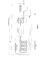
- FIG. 1 is a block diagram of a tunable laser according to an embodiment of the invention.
- FIG. 2 is a block diagram of a tunable laser having a thermal based wavelength reference according to an embodiment of the invention
- FIG. 3 is a block diagram of a tunable laser having a ring topography according to an embodiment of the invention.
- FIG. 4 is a block diagram of a tunable laser outputting lasing light via a drop port of a tunable ring filter according to an embodiment of the invention.
- FIG. 5 is a diagram of an optical system utilizing a plurality of cascaded tunable ring filters according to an embodiment of the invention.
- Embodiments of an apparatus, system and method to utilize a silicon substrate-based tunable laser having a wavelength dependent optical filter and a wavelength reference formed in the silicon substrate are described herein.
- Said silicon-based tunable laser will further have a gain region at least partially formed in the silicon substrate.
- FIG. 1 is a block diagram of a tunable laser according to an embodiment of the invention.
- laser 100 includes tunable ring filter (TRF) 110, gain region 120, phase control region 130, output coupler 140 and stabilized wavelength reference 150.
- TRF tunable ring filter
- the above components may be formed in passive regions of silicon substrate 190, except gain region 120, which may be partially formed in an active region of silicon substrate 190 (in one embodiment described below, gain region 120 further includes III-V semiconductor material).
- TRF 110 selects the wavelength for laser 100.
- TRF 110 includes a tuning region which, when a bias voltage is applied, determines the specific wavelength of the signal received by gain region 120.
- Phase control region 130 may perform fine control of the laser characteristics of light received from gain region 120. For example, phase control region 130 may adjust the resonant cavity modes associated with the tunable laser.
- Output coupler 140 extracts at least a portion of the laser light from phase control region 130, and outputs the laser light. Output coupler 140 may further direct a portion of the light to stabilized wavelength reference 150.
- wavelength reference 150 is used to provide wavelength stability for laser 100.
- Wavelength reference 150 receives a portion of the laser output for output coupler 140 to provide easy and accurate wavelength determination of the laser output.
- Wavelength reference 150 may comprise an etalon, interference filter, grating or any functionally equivalent means that passes light at a known wavelength.
- Wavelength reference 150 may be utilized to determine a difference between the light from the gain region to a known wavelength value. TRF 110 may then be adjusted based, at least in part, on this determined difference in order to tune the output of laser 100 (e.g., via an electrical signal sent from wavelength reference 150).
- gain region 120 comprises a first region of formed in silicon material of substrate 190 and a second region of non-silicon material with high electro-optic efficiency, such as III-V semiconductors. Said regions may be fabricated independently and subsequently bonded via any bonding process known in the art.
- the non-silicon semiconductor region of gain region 120 may at least partially overlap the silicon region to create a lateral overlap region; an optical waveguide of the gain region is included in this lateral overlap region, and the waveguide includes both the silicon and the non-silicon material.
- the refractive index of at least one of the silicon material and the non-silicon material within the optical waveguide may change based on an electrical difference applied to the gain region.
- the above described non-silicon material is a group III - V semiconductor material.
- III-V semiconductors have elements that are found in group III and group V of the periodic table (e.g., Indium Phosphide (InP), Indium Gallium Arsenide Phosphide (InGaAsP), Gallium Indium Arsenide Nitride (GaInAsN)).
- the carrier dispersion effects of III-V based materials may be significantly higher than in silicon based materials for bandgaps closer to the wavelength of the light traversing through gain region 120, as electron speed in III-V semiconductors is much faster than that in silicon.
- III-V semiconductor materials enable photonic operation with an increased efficiency at generating light from electricity and converting light back into electricity.
- the active waveguide of gain region 120 is at least partially formed in (or on) the silicon material of substrate 190, and TRF 110, phase control 130 and wavelength reference 150 are also formed in (or on) the silicon material of the substrate.
- wavelength reference 150 may be formed in or on the silicon material of the substrate by depositing resistive material in or on the silicon, doping the silicon material, or any other functionally equivalent means.
- the tuning efficiency of silicon-based TRFs is higher than III-V semiconductor-based TRFs, and silicon-based TRFs have narrower linewidths.
- III-V semiconductor materials are not as efficient compared to silicon for making low loss, efficient TRFs, while silicon semiconductor materials cannot produce an efficient optical gain without heterogeneous integration of III-V semiconductor material.
- utilizing silicon-based TRFs and having the optical efficiency of III-V semiconductor-based gain regions required packaging of silicon and III-V semiconductor based optical elements, resulting in large optical devices that require a complex manufacturing process. Therefore, embodiments of the invention such as the embodiment illustrated in FIG. 1 eliminate the need for bulk optical elements and hermetic packaging, thereby reducing the size and manufacturing complexity of tunable lasing devices.
- FIG. 2 is a block diagram of a tunable laser having a thermal based wavelength reference according to an embodiment of the invention.
- laser 200 includes TRF 210, gain region 220, phase control region 230 and output coupler 240.
- TRF 210 may include a heating element associated with an optical ring resonator.
- Said heating element may be adjusted, based on optical feedback received from output coupler 240, in order to alter the wavelength of laser light passed to gain region 220; said heating element may also be sized to ensure substantial transfer of heat to the respective optical waveguide, and to limit absorbance by the heating element of optical radiation propagating through the respective optical waveguide.
- TRF 210 includes wave stabilization functionality.
- highly stable thermal sensors are integrated to provide a stable wavelength reference for the wavelength of the laser light passed from TRF 210 to gain region 220.
- the wavelength reference is to be integrated within the laser cavity.
- Highly stable resistive temperature devices (RTDs) formed from silicon substrate 290 may be used to measure the temperature of the wavelength filtering elements.
- the cavity filter is arranged such that changes in the refractive index due to stress are minimized and the temperature is directly related to the laser wavelength and thus, determining the laser wavelength may be done by measuring the temperature of the wavelength filtering elements via the above described RTDs.
- FIG. 3 is a block diagram of a tunable laser having an alternative topography according to an embodiment of the invention.
- laser 300 includes TRF 310, gain 320 and output coupler 330 configured in a ring topography which could produce lower linewidth lasers due to the unidirectional light propogation in the laser (as opposed to the bidirectional light propagation illustrated in FIG. 2 ).
- each of these described elements are either partially or entirely formed in the silicon material of substrate 390.
- FIG. 4 is a block diagram of a tunable laser outputting lasing light via a drop port of a tunable ring filter according to an embodiment of the invention.
- laser 400 includes TRF 410 and gain region 420. As described above, each of these described elements are either partially or entirely formed in the silicon material of substrate 490.
- FIG. 5 is a diagram of an optical system utilizing a plurality of cascaded tunable ring filters according to an embodiment of the invention.
- optical system 500 includes tunable laser 501 and silicon evanescent electro-absorption modulator 502.
- the tunable laser further includes tunable ring feedback coupler 510, silicon evanescent gain 520 and laser output coupler 530.
- Tuning ring feedback coupler 510 may include cascaded ring filters 515.
- the ring filters each have slightly different radii and are laterally coupled to input/output waveguide 540 in a cascaded arrangement. It is understood that varying the radii of ring filters 515 slightly allows for a wide range of tuning for laser 501, due to the Vernier effect (i.e., a large tuning effect is accomplished by exploiting the Vernier effect, by which small relative refractive index changes may be used to yield large relative wavelength changes).
- hybridized III-V/silicon gain region hybrid silicon laser or hybrid ridge lasers
- cascaded Vernier ring filters formed from the silicon material of substrate 590 allow for efficient gain from the III-V region, while providing wide tunability, efficient tunability, and narrow linewidth due to the narrow linewidth nature of silicon rings.
- Modulator 502 may perform either amplitude or phase modulation of the light received from tunable laser 501.
- Modulator 502 may include a waveguide comprising silicon and III-V semiconductor material, similar to the gain regions described above.
- optical system 500 is included in a single device or chip, wherein silicon components of system 500 are included on a silicon portion of the chip, and III-V semiconductor components of system 500 are included on a III-V portion of the chip. Said portions may be fabricated independently and subsequently bonded via any bonding process known in the art.
Landscapes
- Physics & Mathematics (AREA)
- Electromagnetism (AREA)
- Optics & Photonics (AREA)
- Condensed Matter Physics & Semiconductors (AREA)
- General Physics & Mathematics (AREA)
- Engineering & Computer Science (AREA)
- Plasma & Fusion (AREA)
- Automation & Control Theory (AREA)
- Optical Integrated Circuits (AREA)
- Semiconductor Lasers (AREA)
Priority Applications (1)
| Application Number | Priority Date | Filing Date | Title |
|---|---|---|---|
| EP17180806.6A EP3267537B1 (fr) | 2011-09-30 | 2012-10-01 | Laser réglable avec référence de longueur d'onde intégrée |
Applications Claiming Priority (1)
| Application Number | Priority Date | Filing Date | Title |
|---|---|---|---|
| US13/249,753 US9692207B2 (en) | 2011-09-30 | 2011-09-30 | Tunable laser with integrated wavelength reference |
Related Child Applications (2)
| Application Number | Title | Priority Date | Filing Date |
|---|---|---|---|
| EP17180806.6A Division EP3267537B1 (fr) | 2011-09-30 | 2012-10-01 | Laser réglable avec référence de longueur d'onde intégrée |
| EP17180806.6A Division-Into EP3267537B1 (fr) | 2011-09-30 | 2012-10-01 | Laser réglable avec référence de longueur d'onde intégrée |
Publications (3)
| Publication Number | Publication Date |
|---|---|
| EP2575220A2 true EP2575220A2 (fr) | 2013-04-03 |
| EP2575220A3 EP2575220A3 (fr) | 2013-09-18 |
| EP2575220B1 EP2575220B1 (fr) | 2017-08-16 |
Family
ID=47010159
Family Applications (2)
| Application Number | Title | Priority Date | Filing Date |
|---|---|---|---|
| EP12006832.5A Active EP2575220B1 (fr) | 2011-09-30 | 2012-10-01 | Laser accordable avec référence de longueur d'onde intégrée |
| EP17180806.6A Active EP3267537B1 (fr) | 2011-09-30 | 2012-10-01 | Laser réglable avec référence de longueur d'onde intégrée |
Family Applications After (1)
| Application Number | Title | Priority Date | Filing Date |
|---|---|---|---|
| EP17180806.6A Active EP3267537B1 (fr) | 2011-09-30 | 2012-10-01 | Laser réglable avec référence de longueur d'onde intégrée |
Country Status (2)
| Country | Link |
|---|---|
| US (3) | US9692207B2 (fr) |
| EP (2) | EP2575220B1 (fr) |
Cited By (4)
| Publication number | Priority date | Publication date | Assignee | Title |
|---|---|---|---|---|
| FR3020188A1 (fr) * | 2014-04-18 | 2015-10-23 | Commissariat Energie Atomique | Source laser |
| WO2019060547A1 (fr) * | 2017-09-20 | 2019-03-28 | Macom Technology Solutions Holdings, Inc. | Laser accordable pour système de transmission cohérente |
| US11177630B2 (en) | 2018-02-02 | 2021-11-16 | Brolis Sensor Technology, Uab | Wavelength determination for widely tunable lasers and laser systems thereof |
| US11298057B2 (en) | 2017-05-22 | 2022-04-12 | Brolis Sensor Technology, Uab | Tunable hybrid III-V/IV laser sensor system-on-a-chip for real-time monitoring of a blood constituent concentration level |
Families Citing this family (18)
| Publication number | Priority date | Publication date | Assignee | Title |
|---|---|---|---|---|
| CA2872378C (fr) | 2011-07-20 | 2016-01-12 | University Of Washington Through Its Center For Commercialization | Typage de sang photonique |
| US9692207B2 (en) | 2011-09-30 | 2017-06-27 | Aurrion, Inc. | Tunable laser with integrated wavelength reference |
| US10031138B2 (en) | 2012-01-20 | 2018-07-24 | University Of Washington Through Its Center For Commercialization | Hierarchical films having ultra low fouling and high recognition element loading properties |
| US9419412B2 (en) * | 2013-11-13 | 2016-08-16 | Agency For Science, Technology And Research | Integrated laser and method of fabrication thereof |
| US10243328B2 (en) | 2013-11-20 | 2019-03-26 | Elenion Technologies, Llc | Semiconductor laser |
| US9450379B2 (en) | 2013-11-20 | 2016-09-20 | Coriant Advanced Technology, LLC | Quantum dot SOA-silicon external cavity multi-wavelength laser |
| WO2015077472A1 (fr) * | 2013-11-20 | 2015-05-28 | Coriant Advanced Technology, LLC | Cavité laser à miroir à boucle de sagnac sur plate-forme photonique au silicium |
| US9356419B1 (en) | 2015-04-09 | 2016-05-31 | International Business Machines Corporation | Temperature insensitive external cavity lasers on silicon |
| US10411430B1 (en) | 2015-04-20 | 2019-09-10 | Aurrion, Inc. | Optical system and method for locking a wavelength of a tunable laser |
| JP6973480B2 (ja) * | 2017-05-08 | 2021-12-01 | ソニーグループ株式会社 | レーザ装置組立体 |
| CN111819744B (zh) * | 2018-04-09 | 2023-02-03 | 华为技术有限公司 | 波长可调谐激光器 |
| US10527784B1 (en) * | 2018-11-15 | 2020-01-07 | General Electric Company | Systems and methods for providing a stable wavelength reference in an integrated photonic circuit |
| CN110838673A (zh) * | 2019-11-20 | 2020-02-25 | 中国科学院长春光学精密机械与物理研究所 | 一种可调谐窄线宽激光器 |
| US11381053B2 (en) * | 2019-12-18 | 2022-07-05 | Globalfoundries U.S. Inc. | Waveguide-confining layer with gain medium to emit subwavelength lasers, and method to form same |
| US11698308B2 (en) * | 2020-10-05 | 2023-07-11 | Openlight Photonics, Inc. | Optical temperature measurements in photonic circuits |
| CN114552378B (zh) | 2020-11-20 | 2023-03-31 | 中国科学院苏州纳米技术与纳米仿生研究所 | 窄线宽激光器 |
| US12063073B2 (en) | 2021-03-25 | 2024-08-13 | Freedom Photonics Llc | System and method for external wavelength control of optical modulators |
| US12278461B1 (en) * | 2022-02-21 | 2025-04-15 | Insight Photonic Solutions, Inc | System and methods for stable, fast, wide-tuning range hybrid lasers |
Family Cites Families (45)
| Publication number | Priority date | Publication date | Assignee | Title |
|---|---|---|---|---|
| US5267252A (en) * | 1991-08-30 | 1993-11-30 | Hoya Corporation | Solid-state laser device comprising a temperature-controlled thermal conductive support |
| US5349601A (en) * | 1993-09-20 | 1994-09-20 | The United States Of America As Represented By The United States Department Of Energy | Unidirectional ring lasers |
| US6349103B1 (en) | 1997-05-07 | 2002-02-19 | Samsung Electronics Co., Ltd. | Cold-start wavelength-division-multiplexed optical transmission system |
| US6434175B1 (en) | 1999-08-31 | 2002-08-13 | Corning Incorporated | Multiwavelength distributed bragg reflector phased array laser |
| US6633695B2 (en) | 2000-03-06 | 2003-10-14 | Cidra Corporation | Compression-tuned grating-based optical add/drop multiplexer |
| US6714556B1 (en) | 2000-07-17 | 2004-03-30 | Advanced Micro Devices, Inc. | In-band management of a stacked group of switches by a single CPU |
| US6665320B1 (en) | 2001-01-29 | 2003-12-16 | Lightwave Electronics | Wideband tunable laser sources with multiple gain elements |
| JP3929705B2 (ja) * | 2001-02-05 | 2007-06-13 | ユーディナデバイス株式会社 | 半導体装置及びチップキャリア |
| DE60234795D1 (de) | 2001-06-29 | 2010-02-04 | Sumitomo Electric Industries | Pumplichtquelleneinheit, Ramanverstärker und optisches Übertragungssystem |
| EP1291988A1 (fr) | 2001-09-10 | 2003-03-12 | Intune Technologies Limited | Asservissement en fréquence d'un laser à section multiples |
| DE60208416T2 (de) | 2001-10-09 | 2006-06-22 | Infinera Corp., Sunnyvale | Digitale optische netzwerkarchitektur |
| CA2463278C (fr) | 2001-10-09 | 2013-04-02 | Infinera Corporation | Circuits integres photoniques d'emetteurs (txpic) et reseaux de transport optique utilisant lesdits txpic |
| EP1324516B1 (fr) * | 2001-12-21 | 2005-12-14 | Agilent Technologies, Inc. (a Delaware corporation) | Procédé et dispositif de détection de diaphonie |
| KR100515259B1 (ko) | 2002-05-03 | 2005-09-15 | 한국과학기술원 | 파장 가변 광원 구현 방법 및 장치와 이 광원을 이용한 파장분할 다중방식 광전송 장치 |
| US6665321B1 (en) * | 2002-12-31 | 2003-12-16 | Intel Corporation | Tunable laser operation with locally commensurate condition |
| US7181105B2 (en) | 2003-03-25 | 2007-02-20 | Fuji Photo Film Co., Ltd. | Method for adjusting alignment of laser beams in combined-laser-light source where the laser beams are incident on restricted area of light-emission end face of optical fiber |
| EP1811619A3 (fr) | 2003-05-23 | 2007-08-08 | Rohm and Haas Electronic Materials, L.L.C. | Laser à semi-conducteur à cavité externe et son procédé de fabrication |
| TWI251393B (en) * | 2004-03-31 | 2006-03-11 | Nec Corp | Tunable laser |
| US7230963B2 (en) * | 2004-04-14 | 2007-06-12 | The Trustees Of Princeton University | Monolithic wavelength stabilized asymmetric laser |
| US7636522B2 (en) | 2004-04-15 | 2009-12-22 | Infinera Corporation | Coolerless photonic integrated circuits (PICs) for WDM transmission networks and PICs operable with a floating signal channel grid changing with temperature but with fixed channel spacing in the floating grid |
| US7424041B2 (en) * | 2004-04-29 | 2008-09-09 | Avago Technologies Fiber Ip Pte Ltd. | Wide tuneable laser sources |
| US20060039421A1 (en) * | 2004-08-11 | 2006-02-23 | Rong Huang | Thermally Tunable Laser with Single Solid Etalon Wavelength Locker |
| US7414779B2 (en) * | 2005-01-20 | 2008-08-19 | Massachusetts Institute Of Technology | Mode locking methods and apparatus |
| US20060239314A1 (en) * | 2005-04-20 | 2006-10-26 | Hosking Lucy G | Electro-optic transducer die mounted directly upon a temperature sensing device |
| WO2007107187A1 (fr) * | 2006-03-23 | 2007-09-27 | Pirelli & C. S.P.A. | Source optique laser intégrée |
| JP2007271704A (ja) * | 2006-03-30 | 2007-10-18 | Nec Corp | 可変光制御デバイス及び可変光制御方法 |
| WO2008080171A1 (fr) * | 2006-12-22 | 2008-07-03 | Finisar Corporation | Émetteur optique comportant un laser accordable à modulation directe et un élément de remise en forme de spectre optique périodique |
| US7468996B2 (en) | 2006-12-29 | 2008-12-23 | Intel Corporation | External cavity laser tuning element dither servo control |
| JP4892467B2 (ja) | 2007-12-11 | 2012-03-07 | 日本オプネクスト株式会社 | レーザ装置およびその制御方法 |
| US7941014B1 (en) * | 2008-04-09 | 2011-05-10 | Sandia Corporation | Optical waveguide device with an adiabatically-varying width |
| JP2009278015A (ja) | 2008-05-16 | 2009-11-26 | Nec Corp | 平面光波回路及びこれを備えた波長可変レーザ装置 |
| JP2011003591A (ja) * | 2009-06-16 | 2011-01-06 | Sumitomo Electric Ind Ltd | 波長ロッカー集積型半導体レーザ素子 |
| US20110008557A1 (en) * | 2009-07-07 | 2011-01-13 | Zeyfang Frederick W | "Compression-molded silicone rubber cap and plug" |
| US8630326B2 (en) | 2009-10-13 | 2014-01-14 | Skorpios Technologies, Inc. | Method and system of heterogeneous substrate bonding for photonic integration |
| US8615025B2 (en) | 2009-10-13 | 2013-12-24 | Skorpios Technologies, Inc. | Method and system for hybrid integration of a tunable laser |
| US8472805B2 (en) | 2010-05-26 | 2013-06-25 | Google Inc. | Tunable multi-wavelength optical transmitter and transceiver for optical communications based on wavelength division multiplexing |
| US8457165B2 (en) | 2010-05-26 | 2013-06-04 | Google Inc. | Tunable multi-wavelength semiconductor laser array for optical communications based on wavelength division multiplexing |
| KR101405419B1 (ko) * | 2010-06-18 | 2014-06-27 | 한국전자통신연구원 | 레이저 모듈 |
| US8559775B2 (en) | 2010-07-22 | 2013-10-15 | Dubravko Ivan Babic | Colorless optical network architecture and network components |
| US10720350B2 (en) * | 2010-09-28 | 2020-07-21 | Kla-Tencore Corporation | Etch-resistant coating on sensor wafers for in-situ measurement |
| US8467122B2 (en) * | 2011-07-13 | 2013-06-18 | Oracle America, Inc. | Hybrid laser source with ring-resonator reflector |
| US20130016744A1 (en) * | 2011-07-13 | 2013-01-17 | Oracle International Corporation | Laser source with tunable-grating-waveguide reflections |
| US8724667B2 (en) | 2011-07-22 | 2014-05-13 | Insight Photonic Solutions, Inc. | System and method for multiple laser sources using high semiconductor optical amplifier extinction |
| US9692207B2 (en) | 2011-09-30 | 2017-06-27 | Aurrion, Inc. | Tunable laser with integrated wavelength reference |
| US8457465B1 (en) | 2012-05-17 | 2013-06-04 | Google Inc. | Optical attenuation system |
-
2011
- 2011-09-30 US US13/249,753 patent/US9692207B2/en active Active
-
2012
- 2012-10-01 EP EP12006832.5A patent/EP2575220B1/fr active Active
- 2012-10-01 EP EP17180806.6A patent/EP3267537B1/fr active Active
-
2014
- 2014-04-25 US US14/262,502 patent/US9583913B1/en active Active
-
2017
- 2017-01-26 US US15/416,434 patent/US10224695B2/en active Active
Non-Patent Citations (1)
| Title |
|---|
| None |
Cited By (10)
| Publication number | Priority date | Publication date | Assignee | Title |
|---|---|---|---|---|
| FR3020188A1 (fr) * | 2014-04-18 | 2015-10-23 | Commissariat Energie Atomique | Source laser |
| US11298057B2 (en) | 2017-05-22 | 2022-04-12 | Brolis Sensor Technology, Uab | Tunable hybrid III-V/IV laser sensor system-on-a-chip for real-time monitoring of a blood constituent concentration level |
| US11696707B2 (en) | 2017-05-22 | 2023-07-11 | Brolis Sensor Technology, UAB et al. | Tunable hybrid III-V/IV laser sensor system-on-a chip for real-time monitoring of a blood constituent concentration level |
| US11896373B2 (en) | 2017-05-22 | 2024-02-13 | Brolis Sensor Technology, Uab | Tunable hybrid III-V/ IV laser sensor system-on-a chip for real-time monitoring of a blood constituent concentration level |
| WO2019060547A1 (fr) * | 2017-09-20 | 2019-03-28 | Macom Technology Solutions Holdings, Inc. | Laser accordable pour système de transmission cohérente |
| CN111095693A (zh) * | 2017-09-20 | 2020-05-01 | 镁可微波技术有限公司 | 用于相干传输系统的可调谐激光器 |
| US11018477B2 (en) | 2017-09-20 | 2021-05-25 | Macom Technology Solutions Holdings, Inc. | Tunable laser for coherent transmission system |
| CN111095693B (zh) * | 2017-09-20 | 2023-12-19 | 镁可微波技术有限公司 | 用于相干传输系统的可调谐激光器 |
| US11177630B2 (en) | 2018-02-02 | 2021-11-16 | Brolis Sensor Technology, Uab | Wavelength determination for widely tunable lasers and laser systems thereof |
| US11201453B2 (en) | 2018-02-02 | 2021-12-14 | Brolis Sensor Technology, Uab | Wavelength determination for widely tunable lasers and laser systems thereof |
Also Published As
| Publication number | Publication date |
|---|---|
| US9583913B1 (en) | 2017-02-28 |
| US20170141536A1 (en) | 2017-05-18 |
| EP3267537A1 (fr) | 2018-01-10 |
| EP2575220B1 (fr) | 2017-08-16 |
| EP3267537B1 (fr) | 2023-07-19 |
| US9692207B2 (en) | 2017-06-27 |
| US10224695B2 (en) | 2019-03-05 |
| EP2575220A3 (fr) | 2013-09-18 |
| US20130083815A1 (en) | 2013-04-04 |
Similar Documents
| Publication | Publication Date | Title |
|---|---|---|
| US10224695B2 (en) | Method and system for producing wavelength-stabilized light | |
| CN118763500B (zh) | 硅光子外腔可调谐激光器的波长控制方法 | |
| US9653882B1 (en) | Wavelength control of an external cavity laser | |
| US9887780B2 (en) | Chip-based advanced modulation format transmitter | |
| US9318868B2 (en) | Tunable hybrid laser with carrier-induced phase control | |
| US8605766B2 (en) | Method and system for hybrid integration of a tunable laser and a mach zehnder modulator | |
| US8368995B2 (en) | Method and system for hybrid integration of an opto-electronic integrated circuit | |
| US8559470B2 (en) | Method and system for hybrid integration of a tunable laser and a phase modulator | |
| US7257142B2 (en) | Semi-integrated designs for external cavity tunable lasers | |
| US8867578B2 (en) | Method and system for hybrid integration of a tunable laser for a cable TV transmitter | |
| US9436022B2 (en) | Modulated light source | |
| US10666016B2 (en) | Tunable lasers | |
| KR20150128718A (ko) | 결합 링 공진기 시스템 | |
| Porter et al. | Hybrid integrated chip-scale laser systems | |
| CN103904555A (zh) | 光学器件、可调激光器以及实现可调激光器的方法 | |
| US20230361532A1 (en) | Silicon photonic hybrid distributed feedback laser with built-in grating | |
| Kumar et al. | Fully integrated tunable III-V/Si laser with on-chip SOA | |
| US9343869B1 (en) | Mode-hop tolerant semiconductor laser design | |
| Santana et al. | Design of a 80-nm tunable hybrid III/V-on-silicon laser |
Legal Events
| Date | Code | Title | Description |
|---|---|---|---|
| PUAI | Public reference made under article 153(3) epc to a published international application that has entered the european phase |
Free format text: ORIGINAL CODE: 0009012 |
|
| AK | Designated contracting states |
Kind code of ref document: A2 Designated state(s): AL AT BE BG CH CY CZ DE DK EE ES FI FR GB GR HR HU IE IS IT LI LT LU LV MC MK MT NL NO PL PT RO RS SE SI SK SM TR |
|
| AX | Request for extension of the european patent |
Extension state: BA ME |
|
| PUAL | Search report despatched |
Free format text: ORIGINAL CODE: 0009013 |
|
| AK | Designated contracting states |
Kind code of ref document: A3 Designated state(s): AL AT BE BG CH CY CZ DE DK EE ES FI FR GB GR HR HU IE IS IT LI LT LU LV MC MK MT NL NO PL PT RO RS SE SI SK SM TR |
|
| AX | Request for extension of the european patent |
Extension state: BA ME |
|
| RIC1 | Information provided on ipc code assigned before grant |
Ipc: H01S 5/06 20060101AFI20130813BHEP Ipc: H01S 5/026 20060101ALI20130813BHEP |
|
| 17P | Request for examination filed |
Effective date: 20140318 |
|
| RBV | Designated contracting states (corrected) |
Designated state(s): AL AT BE BG CH CY CZ DE DK EE ES FI FR GB GR HR HU IE IS IT LI LT LU LV MC MK MT NL NO PL PT RO RS SE SI SK SM TR |
|
| 17Q | First examination report despatched |
Effective date: 20140924 |
|
| STAA | Information on the status of an ep patent application or granted ep patent |
Free format text: STATUS: EXAMINATION IS IN PROGRESS |
|
| GRAP | Despatch of communication of intention to grant a patent |
Free format text: ORIGINAL CODE: EPIDOSNIGR1 |
|
| STAA | Information on the status of an ep patent application or granted ep patent |
Free format text: STATUS: GRANT OF PATENT IS INTENDED |
|
| INTG | Intention to grant announced |
Effective date: 20170224 |
|
| GRAS | Grant fee paid |
Free format text: ORIGINAL CODE: EPIDOSNIGR3 |
|
| GRAA | (expected) grant |
Free format text: ORIGINAL CODE: 0009210 |
|
| STAA | Information on the status of an ep patent application or granted ep patent |
Free format text: STATUS: THE PATENT HAS BEEN GRANTED |
|
| AK | Designated contracting states |
Kind code of ref document: B1 Designated state(s): AL AT BE BG CH CY CZ DE DK EE ES FI FR GB GR HR HU IE IS IT LI LT LU LV MC MK MT NL NO PL PT RO RS SE SI SK SM TR |
|
| REG | Reference to a national code |
Ref country code: GB Ref legal event code: FG4D |
|
| REG | Reference to a national code |
Ref country code: CH Ref legal event code: EP |
|
| REG | Reference to a national code |
Ref country code: IE Ref legal event code: FG4D |
|
| REG | Reference to a national code |
Ref country code: AT Ref legal event code: REF Ref document number: 919938 Country of ref document: AT Kind code of ref document: T Effective date: 20170915 |
|
| REG | Reference to a national code |
Ref country code: DE Ref legal event code: R096 Ref document number: 602012035885 Country of ref document: DE |
|
| REG | Reference to a national code |
Ref country code: NL Ref legal event code: FP |
|
| REG | Reference to a national code |
Ref country code: FR Ref legal event code: PLFP Year of fee payment: 6 |
|
| REG | Reference to a national code |
Ref country code: LT Ref legal event code: MG4D |
|
| REG | Reference to a national code |
Ref country code: AT Ref legal event code: MK05 Ref document number: 919938 Country of ref document: AT Kind code of ref document: T Effective date: 20170816 |
|
| PG25 | Lapsed in a contracting state [announced via postgrant information from national office to epo] |
Ref country code: SE Free format text: LAPSE BECAUSE OF FAILURE TO SUBMIT A TRANSLATION OF THE DESCRIPTION OR TO PAY THE FEE WITHIN THE PRESCRIBED TIME-LIMIT Effective date: 20170816 Ref country code: AT Free format text: LAPSE BECAUSE OF FAILURE TO SUBMIT A TRANSLATION OF THE DESCRIPTION OR TO PAY THE FEE WITHIN THE PRESCRIBED TIME-LIMIT Effective date: 20170816 Ref country code: LT Free format text: LAPSE BECAUSE OF FAILURE TO SUBMIT A TRANSLATION OF THE DESCRIPTION OR TO PAY THE FEE WITHIN THE PRESCRIBED TIME-LIMIT Effective date: 20170816 Ref country code: NO Free format text: LAPSE BECAUSE OF FAILURE TO SUBMIT A TRANSLATION OF THE DESCRIPTION OR TO PAY THE FEE WITHIN THE PRESCRIBED TIME-LIMIT Effective date: 20171116 Ref country code: FI Free format text: LAPSE BECAUSE OF FAILURE TO SUBMIT A TRANSLATION OF THE DESCRIPTION OR TO PAY THE FEE WITHIN THE PRESCRIBED TIME-LIMIT Effective date: 20170816 |
|
| PG25 | Lapsed in a contracting state [announced via postgrant information from national office to epo] |
Ref country code: GR Free format text: LAPSE BECAUSE OF FAILURE TO SUBMIT A TRANSLATION OF THE DESCRIPTION OR TO PAY THE FEE WITHIN THE PRESCRIBED TIME-LIMIT Effective date: 20171117 Ref country code: LV Free format text: LAPSE BECAUSE OF FAILURE TO SUBMIT A TRANSLATION OF THE DESCRIPTION OR TO PAY THE FEE WITHIN THE PRESCRIBED TIME-LIMIT Effective date: 20170816 Ref country code: ES Free format text: LAPSE BECAUSE OF FAILURE TO SUBMIT A TRANSLATION OF THE DESCRIPTION OR TO PAY THE FEE WITHIN THE PRESCRIBED TIME-LIMIT Effective date: 20170816 Ref country code: BG Free format text: LAPSE BECAUSE OF FAILURE TO SUBMIT A TRANSLATION OF THE DESCRIPTION OR TO PAY THE FEE WITHIN THE PRESCRIBED TIME-LIMIT Effective date: 20171116 Ref country code: PL Free format text: LAPSE BECAUSE OF FAILURE TO SUBMIT A TRANSLATION OF THE DESCRIPTION OR TO PAY THE FEE WITHIN THE PRESCRIBED TIME-LIMIT Effective date: 20170816 Ref country code: IS Free format text: LAPSE BECAUSE OF FAILURE TO SUBMIT A TRANSLATION OF THE DESCRIPTION OR TO PAY THE FEE WITHIN THE PRESCRIBED TIME-LIMIT Effective date: 20171216 Ref country code: RS Free format text: LAPSE BECAUSE OF FAILURE TO SUBMIT A TRANSLATION OF THE DESCRIPTION OR TO PAY THE FEE WITHIN THE PRESCRIBED TIME-LIMIT Effective date: 20170816 |
|
| PGFP | Annual fee paid to national office [announced via postgrant information from national office to epo] |
Ref country code: NL Payment date: 20171026 Year of fee payment: 6 |
|
| PG25 | Lapsed in a contracting state [announced via postgrant information from national office to epo] |
Ref country code: DK Free format text: LAPSE BECAUSE OF FAILURE TO SUBMIT A TRANSLATION OF THE DESCRIPTION OR TO PAY THE FEE WITHIN THE PRESCRIBED TIME-LIMIT Effective date: 20170816 Ref country code: CZ Free format text: LAPSE BECAUSE OF FAILURE TO SUBMIT A TRANSLATION OF THE DESCRIPTION OR TO PAY THE FEE WITHIN THE PRESCRIBED TIME-LIMIT Effective date: 20170816 Ref country code: RO Free format text: LAPSE BECAUSE OF FAILURE TO SUBMIT A TRANSLATION OF THE DESCRIPTION OR TO PAY THE FEE WITHIN THE PRESCRIBED TIME-LIMIT Effective date: 20170816 |
|
| REG | Reference to a national code |
Ref country code: DE Ref legal event code: R097 Ref document number: 602012035885 Country of ref document: DE |
|
| PG25 | Lapsed in a contracting state [announced via postgrant information from national office to epo] |
Ref country code: SK Free format text: LAPSE BECAUSE OF FAILURE TO SUBMIT A TRANSLATION OF THE DESCRIPTION OR TO PAY THE FEE WITHIN THE PRESCRIBED TIME-LIMIT Effective date: 20170816 Ref country code: SM Free format text: LAPSE BECAUSE OF FAILURE TO SUBMIT A TRANSLATION OF THE DESCRIPTION OR TO PAY THE FEE WITHIN THE PRESCRIBED TIME-LIMIT Effective date: 20170816 Ref country code: MC Free format text: LAPSE BECAUSE OF FAILURE TO SUBMIT A TRANSLATION OF THE DESCRIPTION OR TO PAY THE FEE WITHIN THE PRESCRIBED TIME-LIMIT Effective date: 20170816 Ref country code: EE Free format text: LAPSE BECAUSE OF FAILURE TO SUBMIT A TRANSLATION OF THE DESCRIPTION OR TO PAY THE FEE WITHIN THE PRESCRIBED TIME-LIMIT Effective date: 20170816 Ref country code: IT Free format text: LAPSE BECAUSE OF FAILURE TO SUBMIT A TRANSLATION OF THE DESCRIPTION OR TO PAY THE FEE WITHIN THE PRESCRIBED TIME-LIMIT Effective date: 20170816 |
|
| REG | Reference to a national code |
Ref country code: CH Ref legal event code: PL |
|
| PLBE | No opposition filed within time limit |
Free format text: ORIGINAL CODE: 0009261 |
|
| STAA | Information on the status of an ep patent application or granted ep patent |
Free format text: STATUS: NO OPPOSITION FILED WITHIN TIME LIMIT |
|
| 26N | No opposition filed |
Effective date: 20180517 |
|
| REG | Reference to a national code |
Ref country code: IE Ref legal event code: MM4A |
|
| PG25 | Lapsed in a contracting state [announced via postgrant information from national office to epo] |
Ref country code: CH Free format text: LAPSE BECAUSE OF NON-PAYMENT OF DUE FEES Effective date: 20171031 Ref country code: LU Free format text: LAPSE BECAUSE OF NON-PAYMENT OF DUE FEES Effective date: 20171001 Ref country code: LI Free format text: LAPSE BECAUSE OF NON-PAYMENT OF DUE FEES Effective date: 20171031 |
|
| REG | Reference to a national code |
Ref country code: BE Ref legal event code: MM Effective date: 20171031 |
|
| PG25 | Lapsed in a contracting state [announced via postgrant information from national office to epo] |
Ref country code: SI Free format text: LAPSE BECAUSE OF FAILURE TO SUBMIT A TRANSLATION OF THE DESCRIPTION OR TO PAY THE FEE WITHIN THE PRESCRIBED TIME-LIMIT Effective date: 20170816 Ref country code: BE Free format text: LAPSE BECAUSE OF NON-PAYMENT OF DUE FEES Effective date: 20171031 |
|
| PG25 | Lapsed in a contracting state [announced via postgrant information from national office to epo] |
Ref country code: MT Free format text: LAPSE BECAUSE OF NON-PAYMENT OF DUE FEES Effective date: 20171001 |
|
| REG | Reference to a national code |
Ref country code: FR Ref legal event code: PLFP Year of fee payment: 7 |
|
| PG25 | Lapsed in a contracting state [announced via postgrant information from national office to epo] |
Ref country code: IE Free format text: LAPSE BECAUSE OF NON-PAYMENT OF DUE FEES Effective date: 20171001 |
|
| REG | Reference to a national code |
Ref country code: NL Ref legal event code: MM Effective date: 20181101 |
|
| PG25 | Lapsed in a contracting state [announced via postgrant information from national office to epo] |
Ref country code: HU Free format text: LAPSE BECAUSE OF FAILURE TO SUBMIT A TRANSLATION OF THE DESCRIPTION OR TO PAY THE FEE WITHIN THE PRESCRIBED TIME-LIMIT; INVALID AB INITIO Effective date: 20121001 |
|
| PG25 | Lapsed in a contracting state [announced via postgrant information from national office to epo] |
Ref country code: NL Free format text: LAPSE BECAUSE OF NON-PAYMENT OF DUE FEES Effective date: 20181101 |
|
| PG25 | Lapsed in a contracting state [announced via postgrant information from national office to epo] |
Ref country code: CY Free format text: LAPSE BECAUSE OF NON-PAYMENT OF DUE FEES Effective date: 20170816 |
|
| PG25 | Lapsed in a contracting state [announced via postgrant information from national office to epo] |
Ref country code: MK Free format text: LAPSE BECAUSE OF FAILURE TO SUBMIT A TRANSLATION OF THE DESCRIPTION OR TO PAY THE FEE WITHIN THE PRESCRIBED TIME-LIMIT Effective date: 20170816 |
|
| PG25 | Lapsed in a contracting state [announced via postgrant information from national office to epo] |
Ref country code: TR Free format text: LAPSE BECAUSE OF FAILURE TO SUBMIT A TRANSLATION OF THE DESCRIPTION OR TO PAY THE FEE WITHIN THE PRESCRIBED TIME-LIMIT Effective date: 20170816 |
|
| PG25 | Lapsed in a contracting state [announced via postgrant information from national office to epo] |
Ref country code: PT Free format text: LAPSE BECAUSE OF FAILURE TO SUBMIT A TRANSLATION OF THE DESCRIPTION OR TO PAY THE FEE WITHIN THE PRESCRIBED TIME-LIMIT Effective date: 20170816 |
|
| PG25 | Lapsed in a contracting state [announced via postgrant information from national office to epo] |
Ref country code: HR Free format text: LAPSE BECAUSE OF FAILURE TO SUBMIT A TRANSLATION OF THE DESCRIPTION OR TO PAY THE FEE WITHIN THE PRESCRIBED TIME-LIMIT Effective date: 20170816 |
|
| PG25 | Lapsed in a contracting state [announced via postgrant information from national office to epo] |
Ref country code: AL Free format text: LAPSE BECAUSE OF FAILURE TO SUBMIT A TRANSLATION OF THE DESCRIPTION OR TO PAY THE FEE WITHIN THE PRESCRIBED TIME-LIMIT Effective date: 20170816 |
|
| REG | Reference to a national code |
Ref country code: DE Ref legal event code: R081 Ref document number: 602012035885 Country of ref document: DE Owner name: OPENLIGHT PHOTONICS, INC., GOLETA, US Free format text: FORMER OWNER: AURRION, INC., GOLETA, CALIF., US |
|
| PGFP | Annual fee paid to national office [announced via postgrant information from national office to epo] |
Ref country code: DE Payment date: 20251010 Year of fee payment: 14 |
|
| PGFP | Annual fee paid to national office [announced via postgrant information from national office to epo] |
Ref country code: GB Payment date: 20251013 Year of fee payment: 14 |
|
| PGFP | Annual fee paid to national office [announced via postgrant information from national office to epo] |
Ref country code: FR Payment date: 20251014 Year of fee payment: 14 |