EP2575207A1 - Elektronisches Kommunikationsgerät und Antennenstruktur dafür - Google Patents
Elektronisches Kommunikationsgerät und Antennenstruktur dafür Download PDFInfo
- Publication number
- EP2575207A1 EP2575207A1 EP12156286A EP12156286A EP2575207A1 EP 2575207 A1 EP2575207 A1 EP 2575207A1 EP 12156286 A EP12156286 A EP 12156286A EP 12156286 A EP12156286 A EP 12156286A EP 2575207 A1 EP2575207 A1 EP 2575207A1
- Authority
- EP
- European Patent Office
- Prior art keywords
- notch
- antenna
- antenna structure
- electronic device
- grounding element
- Prior art date
- Legal status (The legal status is an assumption and is not a legal conclusion. Google has not performed a legal analysis and makes no representation as to the accuracy of the status listed.)
- Granted
Links
Images


Classifications
-
- H—ELECTRICITY
- H01—ELECTRIC ELEMENTS
- H01Q—ANTENNAS, i.e. RADIO AERIALS
- H01Q1/00—Details of, or arrangements associated with, antennas
- H01Q1/12—Supports; Mounting means
- H01Q1/22—Supports; Mounting means by structural association with other equipment or articles
- H01Q1/24—Supports; Mounting means by structural association with other equipment or articles with receiving set
- H01Q1/241—Supports; Mounting means by structural association with other equipment or articles with receiving set used in mobile communications, e.g. GSM
- H01Q1/242—Supports; Mounting means by structural association with other equipment or articles with receiving set used in mobile communications, e.g. GSM specially adapted for hand-held use
- H01Q1/243—Supports; Mounting means by structural association with other equipment or articles with receiving set used in mobile communications, e.g. GSM specially adapted for hand-held use with built-in antennas
-
- H—ELECTRICITY
- H01—ELECTRIC ELEMENTS
- H01Q—ANTENNAS, i.e. RADIO AERIALS
- H01Q1/00—Details of, or arrangements associated with, antennas
- H01Q1/48—Earthing means; Earth screens; Counterpoises
Definitions
- the present invention relates to an antenna structure according to the pre-characterizing clause of Claim 1.
- a communication electronic device with a multiband loop antenna wherein the loop antenna is disposed in an edge of the grounding element and occupies the overall edge in order to achieve a wide band operation.
- Such an antenna configuration cannot be tightly combined with peripheral electronic elements, which results in a waste of interior space of the device. Also, since the distance between the user's hand and the antenna element is smaller when the communication electronic device is in use, the radiation efficiency of the antenna may be easily affected by the user's hand.
- a communication electronic device having an antenna with two wide operating bands at least covering from 824 MHz to 960 MHz and from 1710 MHz to 2170 MHz to satisfy the five-band WWAN operation has become an important topic in this field.
- the invention aims at providing a communication electronic device and an antenna structure for reducing influences resulting from a user's hand when the communication electronic device is in use, and enabling the antenna element to be tightly integrated with peripheral electronic elements (such as data transfer ports).
- the antenna structure may include a grounding element and an antenna element. There is a first notch, a second notch and a first protruded portion disposed at an edge of the grounding element, wherein the first notch and the second notch are not located at corners of the edge of the grounding element, and the first protruded portion is located between the first notch and the second notch.
- the antenna element and the grounding element are disposed on different planes.
- the antenna element has a projection on the grounding element, and the projection covers a portion of the first protruded portion, a portion of the first notch, and a portion of the second notch.
- the antenna structure may be disposed in a communication electronic device.
- the antenna element of the present invention adopts a loop antenna having a closed loop, and having a first operating band and a second operating band.
- the loop antenna can be coupled to the grounding element through the shorting end in order to excite a resonant mode for forming a first operating band, wherein the resonant length is equal to a half-wavelength of a center frequency of the first operating band. Additionally, a full-wavelength resonant mode can be excited by the loop antenna so as to form the second operating band.
- the first operating band covers about 824MHz to 960MHz
- the second operating band covers about 1710MHz to 2170MHz.
- FIG. 1 is a diagram illustrating a communication electronic device 1 and an antenna structure disposed therein according to a first embodiment of the present invention
- FIG. 2 is a diagram illustrating the grounding element of the communication electronic device 1 according to a first embodiment of the present invention.
- the communication electronic device 1 may include a grounding element 10 and an antenna element 11.
- the first notch 102 and the second notch 103 are not located at corners of the edge 101 of the grounding element 10; and the first protruded portion 104 is located between the first notch 102 and the second notch 103.
- the grounding element 10 forms an inverted E shape.
- the antenna element 11 and the grounding element 10 are disposed on different planes, and thus the antenna element 11 has a projection 21 on the grounding element 10 (as is shown in FIG. 2 ), wherein the projection 21 covers a portion of the first protruded portion 104, a portion of the first notch 102, and a portion of the second notch 103.
- the first protruded portion 104 is used for accommodating an electronic element 16.
- the antenna element 11 may include a substrate 12, a shorted loop strip 13, and a feeding portion 14, but this in no way should be considered as a limitation of the present invention.
- the shorted loop strip 13 forms a closed loop and has a shorting end 131, and the shorted loop strip 13 is electronically connected to the grounding element 10 through the shorting end 131.
- the feeding portion 14 may include a feeding end 141 electronically connected to a signal source 15, wherein the feeding portion 14 is arranged for exciting the shorted loop strip 13.
- the shorted loop strip 13 at least partially surrounds the feeding portion 14.
- a coupling gap D exists between the shorted loop strip 13 and the feeding portion 14, and the coupling gap D is about 0.5 mm.
- the feeding portion 14 shown in the first embodiment forms a T shape.
- FIG. 3 is a diagram illustrating the return loss of the communication electronic device 1 and the antenna structure disposed therein according to a first embodiment of the present invention.
- the size of the communication electronic device 1 is as follows: the grounding element 10 has a length of 115 mm and a width of 60 mm; the first notch 102 has a width of 20 mm and a depth of 10 mm; the second notch 103 has a width of 20 mm and a depth of 10 mm, wherein both the first notch 102 and the second notch 103 are not located at corners of the edge 101 of the grounding element 10; the first protruded portion 104 has a width of 10 mm and a length of 10 mm; the shorted loop strip 13 has a length of 150 mm; and the projection 21 of the antenna element 11 on the grounding element 10 has a size of 10x42 mm 2 .
- the first operating band 31 of the communication electronic device 1 and its antenna structure may cover the two-band GSM850/900 operation (from about 824 MHz to 960 MHz), and the second operating band 32 may cover the three-band GSM1800/1900/UMTS operation (from about 1710 MHz to 2170 MHz), thereby the antenna structure can satisfy requirements of the five-band WWAN operation.
- the shorted loop strip 13 is excited through the feeding portion 14, such that a half-wavelength resonant mode is excited at the lower frequencies (around 860MHz) in order to form a wideband first operating band 31 at least covering 824MHz to 960MHz, and a higher-order resonant mode is excited at the higher frequencies (such as 1800MHz).
- a higher-frequency resonant mode can be excited by the feeding portion 14 at around 2000MHz, and these two higher-frequency resonant modes are combined to form a wideband second operating band 32 at least covering 1710MHz to 2170MHz.
- the shorted loop strip 13 forms a closed metal loop having a balanced characteristic for reducing the coupling effect between the antenna element 11 and the grounding element 10 or surroundings, such that the antenna element 11 can be tightly combined with the adjacent grounding element 10 and has a lower near-field radiation. Since the antenna element 11 is surrounded by the first notch 102 and the second notch 103 of the grounding element 10, the coupling effect resulting from the user's hand and the antenna element 11 can be reduced when the communication electronic device 1 is in use.
- the first protruded portion 104 can be further used for accommodating an electronic element 16 (such as a data transfer port), such that the antenna structure can be tightly integrated with peripheral electronic elements, has a simple structure and can be manufactured easily, which can satisfy requirements of practical applications.
- an electronic element 16 such as a data transfer port
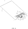
- FIG. 4 is a diagram illustrating a communication electronic device 4 and an antenna structure disposed therein according to a second embodiment of the present invention.
- the structure of the communication electronic device 4 shown in the second embodiment is similar to that of the communication electronic device 1 shown in the first embodiment, and the difference between them is that: an antenna element 41 (including a shorted loop strip 43 and a feeding portion 44) of the communication electronic device 4 shown in FIG. 4 does not to be disposed on the substrate.
- the antenna element 41 can be manufactured by cutting a metal sheet directly so as to increase its manufacture flexibility.
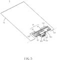
- FIG. 5 is a diagram illustrating a communication electronic device 5 and an antenna structure disposed therein according to a third embodiment of the present invention.
- the structure of the communication electronic device 5 shown in the third embodiment is similar to that of the communication electronic device 1 shown in the first embodiment, and the difference between them is that: an electronic element 56 shown in FIG. 5 is located between the antenna element 51 (including a shorted loop strip 53 and a feeding portion 54) and the first protruded portion 104 so as to reduce the whole thickness of the communication electronic device 5.
- the feeding portion 54 forms an L shape. In other words, the shape of the feeding portion 14/44/54 of the antenna element 11/41/51 is not limited.
- either the structure of the communication electronic device 4 of the second embodiment or the structure of the communication electronic device 5 of the third embodiment is similar to that of the communication electronic device 1 of the first embodiment, and forms two similar wideband operating bands covering the five-band WWAN operation.
- a communication electronic device and its antenna structure which include an antenna element capable of forming two wide operating bands.
- Such an antenna structure has a simple structure and a lower near-field radiation, such that the coupling effect resulting from the user's hand can be reduced when the communication electronic device is in use, and the antenna element can be tightly integrated with adjacent electronic elements.
- the two operating bands of the antenna structure may cover the two-band GSM850/900 operation (from about 824 MHz to 960 MHz) and the three-band GSM1800/1900/UMTS operation (from about 1710 MHz to 2170 MHz), respectively, thereby satisfying requirements of the five-band WWAN operation.
Landscapes
- Engineering & Computer Science (AREA)
- Computer Networks & Wireless Communication (AREA)
- Support Of Aerials (AREA)
- Details Of Aerials (AREA)
- Waveguide Aerials (AREA)
Applications Claiming Priority (1)
| Application Number | Priority Date | Filing Date | Title |
|---|---|---|---|
| TW100134786A TWI488357B (zh) | 2011-09-27 | 2011-09-27 | 通訊電子裝置及其天線結構 |
Publications (2)
| Publication Number | Publication Date |
|---|---|
| EP2575207A1 true EP2575207A1 (de) | 2013-04-03 |
| EP2575207B1 EP2575207B1 (de) | 2014-05-14 |
Family
ID=45656248
Family Applications (1)
| Application Number | Title | Priority Date | Filing Date |
|---|---|---|---|
| EP12156286.2A Active EP2575207B1 (de) | 2011-09-27 | 2012-02-21 | Elektronisches Kommunikationsgerät und Antennenstruktur dafür |
Country Status (5)
| Country | Link |
|---|---|
| US (1) | US8890762B2 (de) |
| EP (1) | EP2575207B1 (de) |
| JP (1) | JP2013074619A (de) |
| KR (1) | KR101331475B1 (de) |
| TW (1) | TWI488357B (de) |
Cited By (1)
| Publication number | Priority date | Publication date | Assignee | Title |
|---|---|---|---|---|
| US8922448B2 (en) | 2012-09-26 | 2014-12-30 | Mediatek Singapore Pte. Ltd. | Communication device and antennas with high isolation characteristics |
Families Citing this family (10)
| Publication number | Priority date | Publication date | Assignee | Title |
|---|---|---|---|---|
| KR101292482B1 (ko) * | 2012-03-08 | 2013-07-31 | 주식회사 팬택 | 안테나를 포함하는 단말기 |
| GB2532315B (en) * | 2014-09-05 | 2019-04-17 | Smart Antenna Tech Limited | Compact antenna array configured for signal isolation between the antenna element ports |
| GB2529884B (en) | 2014-09-05 | 2017-09-13 | Smart Antenna Tech Ltd | Reconfigurable multi-band antenna with independent control |
| TWI605635B (zh) * | 2015-03-16 | 2017-11-11 | 耀登科技股份有限公司 | 通訊裝置 |
| TWI563734B (en) * | 2015-07-07 | 2016-12-21 | Arcadyan Technology Corp | Printed multi-band antenna |
| JP6531544B2 (ja) * | 2015-07-27 | 2019-06-19 | 富士通株式会社 | アンテナ装置 |
| CN106374226B (zh) * | 2016-09-30 | 2024-04-16 | 深圳市信维通信股份有限公司 | 用于第五代无线通信的双频阵列天线 |
| DE102019205556A1 (de) * | 2019-04-17 | 2020-10-22 | BSH Hausgeräte GmbH | Leiterplatten-Antenne |
| CN110165377B (zh) * | 2019-06-03 | 2021-04-27 | Oppo广东移动通信有限公司 | 一种天线组件及电子设备 |
| TWI765743B (zh) * | 2021-06-11 | 2022-05-21 | 啓碁科技股份有限公司 | 天線結構 |
Citations (5)
| Publication number | Priority date | Publication date | Assignee | Title |
|---|---|---|---|---|
| WO2004001894A1 (en) * | 2002-06-25 | 2003-12-31 | Fractus, S.A. | Multiband antenna for handheld terminal |
| EP1401050A1 (de) * | 2002-09-19 | 2004-03-24 | Filtronic LK Oy | Interne Antenne |
| EP1562259A1 (de) * | 2004-02-06 | 2005-08-10 | Kabushiki Kaisha Toshiba | Funkkommunikationsvorrichtung |
| US7768466B2 (en) | 2008-04-09 | 2010-08-03 | Acer Incorporated | Multiband folded loop antenna |
| US20100225544A1 (en) * | 2007-05-16 | 2010-09-09 | Toru Taura | Slot antenna and portable wireless terminal |
Family Cites Families (7)
| Publication number | Priority date | Publication date | Assignee | Title |
|---|---|---|---|---|
| EP0954051B1 (de) | 1998-04-28 | 2003-07-09 | Asulab S.A. | Schlitzantenne, insbesondere für eine Uhr |
| US7138948B2 (en) | 2004-11-19 | 2006-11-21 | Alpha Networks Inc. | Antenna array of printed circuit board |
| US7385561B2 (en) * | 2005-02-17 | 2008-06-10 | Galtronics Ltd. | Multiple monopole antenna |
| US7450072B2 (en) | 2006-03-28 | 2008-11-11 | Qualcomm Incorporated | Modified inverted-F antenna for wireless communication |
| KR101442503B1 (ko) * | 2006-11-16 | 2014-09-24 | 갈트로닉스 코포레이션 리미티드 | 컴팩트 안테나 |
| TWI423526B (zh) * | 2009-06-29 | 2014-01-11 | Acer Inc | 一種多頻天線 |
| CN101997165B (zh) | 2010-10-27 | 2014-07-30 | 惠州Tcl移动通信有限公司 | 一种封闭型多频段天线及其无线通讯装置 |
-
2011
- 2011-09-27 TW TW100134786A patent/TWI488357B/zh active
- 2011-12-11 US US13/316,547 patent/US8890762B2/en active Active
-
2012
- 2012-01-11 KR KR1020120003358A patent/KR101331475B1/ko not_active Expired - Fee Related
- 2012-01-17 JP JP2012007052A patent/JP2013074619A/ja active Pending
- 2012-02-21 EP EP12156286.2A patent/EP2575207B1/de active Active
Patent Citations (5)
| Publication number | Priority date | Publication date | Assignee | Title |
|---|---|---|---|---|
| WO2004001894A1 (en) * | 2002-06-25 | 2003-12-31 | Fractus, S.A. | Multiband antenna for handheld terminal |
| EP1401050A1 (de) * | 2002-09-19 | 2004-03-24 | Filtronic LK Oy | Interne Antenne |
| EP1562259A1 (de) * | 2004-02-06 | 2005-08-10 | Kabushiki Kaisha Toshiba | Funkkommunikationsvorrichtung |
| US20100225544A1 (en) * | 2007-05-16 | 2010-09-09 | Toru Taura | Slot antenna and portable wireless terminal |
| US7768466B2 (en) | 2008-04-09 | 2010-08-03 | Acer Incorporated | Multiband folded loop antenna |
Cited By (2)
| Publication number | Priority date | Publication date | Assignee | Title |
|---|---|---|---|---|
| US8922448B2 (en) | 2012-09-26 | 2014-12-30 | Mediatek Singapore Pte. Ltd. | Communication device and antennas with high isolation characteristics |
| DE102013100731B4 (de) | 2012-09-26 | 2018-10-11 | Mediatek Singapore Pte. Ltd. | Kommunikationsgerät und Antennen mit hohen Isolationseigenschaften |
Also Published As
| Publication number | Publication date |
|---|---|
| EP2575207B1 (de) | 2014-05-14 |
| KR101331475B1 (ko) | 2013-11-20 |
| TWI488357B (zh) | 2015-06-11 |
| US8890762B2 (en) | 2014-11-18 |
| KR20130033930A (ko) | 2013-04-04 |
| US20130076587A1 (en) | 2013-03-28 |
| JP2013074619A (ja) | 2013-04-22 |
| TW201315015A (zh) | 2013-04-01 |
Similar Documents
| Publication | Publication Date | Title |
|---|---|---|
| EP2575207A1 (de) | Elektronisches Kommunikationsgerät und Antennenstruktur dafür | |
| US8933852B2 (en) | Mobile communication device and antenna structure therein | |
| EP2555320A1 (de) | Elektronische Kommunikationsvorrichtung und Antennenstruktur darin | |
| CN104795623B (zh) | 移动装置及其制造方法 | |
| US8723740B2 (en) | Portable electronic device | |
| US8836582B2 (en) | Mobile communication device and antenna structure therein | |
| CN101258641A (zh) | 带有平面带元件的内置多波段天线 | |
| AU2012200663A1 (en) | Mobile communication device and antenna structure thereof | |
| CN112448156A (zh) | 天线结构 | |
| US8947314B2 (en) | Mobile communication device and built-in antenna integrated with a ground portion thereof | |
| EP2648273A1 (de) | Kommunikationsvorrichtung mit leitendem Gehäuse und Antennenelement darin | |
| EP2728665B1 (de) | Kommunikationsvorrichtung und Breitbandantennenelement darin | |
| EP2157661B1 (de) | Dualbandantenne | |
| EP2755277B1 (de) | Kommunikationsvorrichtung und Antennenelement darin | |
| CN104577298A (zh) | 通信装置 | |
| CN112397888A (zh) | 移动装置 | |
| CN103811850B (zh) | 通信装置 | |
| CN103928755B (zh) | 通信装置 | |
| CN110931938B (zh) | 电子装置 | |
| EP2752939B1 (de) | Kommunikationsvorrichtung mit Antennenelementen | |
| CN112993542A (zh) | 天线系统 | |
| CN103036583A (zh) | 通信电子装置及其天线结构 | |
| US8816926B2 (en) | Antenna structure | |
| CN101536250A (zh) | 寄生天线 | |
| CN111564694A (zh) | 天线结构 |
Legal Events
| Date | Code | Title | Description |
|---|---|---|---|
| PUAI | Public reference made under article 153(3) epc to a published international application that has entered the european phase |
Free format text: ORIGINAL CODE: 0009012 |
|
| AK | Designated contracting states |
Kind code of ref document: A1 Designated state(s): AL AT BE BG CH CY CZ DE DK EE ES FI FR GB GR HR HU IE IS IT LI LT LU LV MC MK MT NL NO PL PT RO RS SE SI SK SM TR |
|
| AX | Request for extension of the european patent |
Extension state: BA ME |
|
| 17P | Request for examination filed |
Effective date: 20130425 |
|
| GRAP | Despatch of communication of intention to grant a patent |
Free format text: ORIGINAL CODE: EPIDOSNIGR1 |
|
| INTG | Intention to grant announced |
Effective date: 20131220 |
|
| GRAS | Grant fee paid |
Free format text: ORIGINAL CODE: EPIDOSNIGR3 |
|
| GRAA | (expected) grant |
Free format text: ORIGINAL CODE: 0009210 |
|
| AK | Designated contracting states |
Kind code of ref document: B1 Designated state(s): AL AT BE BG CH CY CZ DE DK EE ES FI FR GB GR HR HU IE IS IT LI LT LU LV MC MK MT NL NO PL PT RO RS SE SI SK SM TR |
|
| REG | Reference to a national code |
Ref country code: GB Ref legal event code: FG4D |
|
| REG | Reference to a national code |
Ref country code: AT Ref legal event code: REF Ref document number: 668891 Country of ref document: AT Kind code of ref document: T Effective date: 20140615 |
|
| REG | Reference to a national code |
Ref country code: IE Ref legal event code: FG4D |
|
| REG | Reference to a national code |
Ref country code: DE Ref legal event code: R096 Ref document number: 602012001624 Country of ref document: DE Effective date: 20140626 |
|
| REG | Reference to a national code |
Ref country code: NL Ref legal event code: VDEP Effective date: 20140514 Ref country code: AT Ref legal event code: MK05 Ref document number: 668891 Country of ref document: AT Kind code of ref document: T Effective date: 20140514 |
|
| REG | Reference to a national code |
Ref country code: LT Ref legal event code: MG4D |
|
| PG25 | Lapsed in a contracting state [announced via postgrant information from national office to epo] |
Ref country code: GR Free format text: LAPSE BECAUSE OF FAILURE TO SUBMIT A TRANSLATION OF THE DESCRIPTION OR TO PAY THE FEE WITHIN THE PRESCRIBED TIME-LIMIT Effective date: 20140815 Ref country code: IS Free format text: LAPSE BECAUSE OF FAILURE TO SUBMIT A TRANSLATION OF THE DESCRIPTION OR TO PAY THE FEE WITHIN THE PRESCRIBED TIME-LIMIT Effective date: 20140914 Ref country code: FI Free format text: LAPSE BECAUSE OF FAILURE TO SUBMIT A TRANSLATION OF THE DESCRIPTION OR TO PAY THE FEE WITHIN THE PRESCRIBED TIME-LIMIT Effective date: 20140514 Ref country code: CY Free format text: LAPSE BECAUSE OF FAILURE TO SUBMIT A TRANSLATION OF THE DESCRIPTION OR TO PAY THE FEE WITHIN THE PRESCRIBED TIME-LIMIT Effective date: 20140514 Ref country code: LT Free format text: LAPSE BECAUSE OF FAILURE TO SUBMIT A TRANSLATION OF THE DESCRIPTION OR TO PAY THE FEE WITHIN THE PRESCRIBED TIME-LIMIT Effective date: 20140514 Ref country code: NO Free format text: LAPSE BECAUSE OF FAILURE TO SUBMIT A TRANSLATION OF THE DESCRIPTION OR TO PAY THE FEE WITHIN THE PRESCRIBED TIME-LIMIT Effective date: 20140814 |
|
| PG25 | Lapsed in a contracting state [announced via postgrant information from national office to epo] |
Ref country code: ES Free format text: LAPSE BECAUSE OF FAILURE TO SUBMIT A TRANSLATION OF THE DESCRIPTION OR TO PAY THE FEE WITHIN THE PRESCRIBED TIME-LIMIT Effective date: 20140514 Ref country code: LV Free format text: LAPSE BECAUSE OF FAILURE TO SUBMIT A TRANSLATION OF THE DESCRIPTION OR TO PAY THE FEE WITHIN THE PRESCRIBED TIME-LIMIT Effective date: 20140514 Ref country code: SE Free format text: LAPSE BECAUSE OF FAILURE TO SUBMIT A TRANSLATION OF THE DESCRIPTION OR TO PAY THE FEE WITHIN THE PRESCRIBED TIME-LIMIT Effective date: 20140514 Ref country code: PL Free format text: LAPSE BECAUSE OF FAILURE TO SUBMIT A TRANSLATION OF THE DESCRIPTION OR TO PAY THE FEE WITHIN THE PRESCRIBED TIME-LIMIT Effective date: 20140514 Ref country code: RS Free format text: LAPSE BECAUSE OF FAILURE TO SUBMIT A TRANSLATION OF THE DESCRIPTION OR TO PAY THE FEE WITHIN THE PRESCRIBED TIME-LIMIT Effective date: 20140514 Ref country code: HR Free format text: LAPSE BECAUSE OF FAILURE TO SUBMIT A TRANSLATION OF THE DESCRIPTION OR TO PAY THE FEE WITHIN THE PRESCRIBED TIME-LIMIT Effective date: 20140514 Ref country code: AT Free format text: LAPSE BECAUSE OF FAILURE TO SUBMIT A TRANSLATION OF THE DESCRIPTION OR TO PAY THE FEE WITHIN THE PRESCRIBED TIME-LIMIT Effective date: 20140514 |
|
| PG25 | Lapsed in a contracting state [announced via postgrant information from national office to epo] |
Ref country code: PT Free format text: LAPSE BECAUSE OF FAILURE TO SUBMIT A TRANSLATION OF THE DESCRIPTION OR TO PAY THE FEE WITHIN THE PRESCRIBED TIME-LIMIT Effective date: 20140915 |
|
| PG25 | Lapsed in a contracting state [announced via postgrant information from national office to epo] |
Ref country code: DK Free format text: LAPSE BECAUSE OF FAILURE TO SUBMIT A TRANSLATION OF THE DESCRIPTION OR TO PAY THE FEE WITHIN THE PRESCRIBED TIME-LIMIT Effective date: 20140514 Ref country code: CZ Free format text: LAPSE BECAUSE OF FAILURE TO SUBMIT A TRANSLATION OF THE DESCRIPTION OR TO PAY THE FEE WITHIN THE PRESCRIBED TIME-LIMIT Effective date: 20140514 Ref country code: EE Free format text: LAPSE BECAUSE OF FAILURE TO SUBMIT A TRANSLATION OF THE DESCRIPTION OR TO PAY THE FEE WITHIN THE PRESCRIBED TIME-LIMIT Effective date: 20140514 Ref country code: BE Free format text: LAPSE BECAUSE OF FAILURE TO SUBMIT A TRANSLATION OF THE DESCRIPTION OR TO PAY THE FEE WITHIN THE PRESCRIBED TIME-LIMIT Effective date: 20140514 Ref country code: SK Free format text: LAPSE BECAUSE OF FAILURE TO SUBMIT A TRANSLATION OF THE DESCRIPTION OR TO PAY THE FEE WITHIN THE PRESCRIBED TIME-LIMIT Effective date: 20140514 Ref country code: RO Free format text: LAPSE BECAUSE OF FAILURE TO SUBMIT A TRANSLATION OF THE DESCRIPTION OR TO PAY THE FEE WITHIN THE PRESCRIBED TIME-LIMIT Effective date: 20140514 |
|
| REG | Reference to a national code |
Ref country code: DE Ref legal event code: R097 Ref document number: 602012001624 Country of ref document: DE |
|
| PG25 | Lapsed in a contracting state [announced via postgrant information from national office to epo] |
Ref country code: NL Free format text: LAPSE BECAUSE OF FAILURE TO SUBMIT A TRANSLATION OF THE DESCRIPTION OR TO PAY THE FEE WITHIN THE PRESCRIBED TIME-LIMIT Effective date: 20140514 |
|
| PLBE | No opposition filed within time limit |
Free format text: ORIGINAL CODE: 0009261 |
|
| STAA | Information on the status of an ep patent application or granted ep patent |
Free format text: STATUS: NO OPPOSITION FILED WITHIN TIME LIMIT |
|
| 26N | No opposition filed |
Effective date: 20150217 |
|
| PG25 | Lapsed in a contracting state [announced via postgrant information from national office to epo] |
Ref country code: IT Free format text: LAPSE BECAUSE OF FAILURE TO SUBMIT A TRANSLATION OF THE DESCRIPTION OR TO PAY THE FEE WITHIN THE PRESCRIBED TIME-LIMIT Effective date: 20140514 |
|
| REG | Reference to a national code |
Ref country code: DE Ref legal event code: R097 Ref document number: 602012001624 Country of ref document: DE Effective date: 20150217 |
|
| PG25 | Lapsed in a contracting state [announced via postgrant information from national office to epo] |
Ref country code: SI Free format text: LAPSE BECAUSE OF FAILURE TO SUBMIT A TRANSLATION OF THE DESCRIPTION OR TO PAY THE FEE WITHIN THE PRESCRIBED TIME-LIMIT Effective date: 20140514 |
|
| PG25 | Lapsed in a contracting state [announced via postgrant information from national office to epo] |
Ref country code: LU Free format text: LAPSE BECAUSE OF FAILURE TO SUBMIT A TRANSLATION OF THE DESCRIPTION OR TO PAY THE FEE WITHIN THE PRESCRIBED TIME-LIMIT Effective date: 20150221 |
|
| REG | Reference to a national code |
Ref country code: CH Ref legal event code: PL |
|
| PG25 | Lapsed in a contracting state [announced via postgrant information from national office to epo] |
Ref country code: CH Free format text: LAPSE BECAUSE OF NON-PAYMENT OF DUE FEES Effective date: 20150228 Ref country code: MC Free format text: LAPSE BECAUSE OF FAILURE TO SUBMIT A TRANSLATION OF THE DESCRIPTION OR TO PAY THE FEE WITHIN THE PRESCRIBED TIME-LIMIT Effective date: 20140514 Ref country code: LI Free format text: LAPSE BECAUSE OF NON-PAYMENT OF DUE FEES Effective date: 20150228 |
|
| REG | Reference to a national code |
Ref country code: IE Ref legal event code: MM4A |
|
| REG | Reference to a national code |
Ref country code: FR Ref legal event code: PLFP Year of fee payment: 5 |
|
| PG25 | Lapsed in a contracting state [announced via postgrant information from national office to epo] |
Ref country code: IE Free format text: LAPSE BECAUSE OF NON-PAYMENT OF DUE FEES Effective date: 20150221 |
|
| PG25 | Lapsed in a contracting state [announced via postgrant information from national office to epo] |
Ref country code: MT Free format text: LAPSE BECAUSE OF FAILURE TO SUBMIT A TRANSLATION OF THE DESCRIPTION OR TO PAY THE FEE WITHIN THE PRESCRIBED TIME-LIMIT Effective date: 20140514 |
|
| REG | Reference to a national code |
Ref country code: FR Ref legal event code: PLFP Year of fee payment: 6 |
|
| PG25 | Lapsed in a contracting state [announced via postgrant information from national office to epo] |
Ref country code: HU Free format text: LAPSE BECAUSE OF FAILURE TO SUBMIT A TRANSLATION OF THE DESCRIPTION OR TO PAY THE FEE WITHIN THE PRESCRIBED TIME-LIMIT; INVALID AB INITIO Effective date: 20120221 Ref country code: SM Free format text: LAPSE BECAUSE OF FAILURE TO SUBMIT A TRANSLATION OF THE DESCRIPTION OR TO PAY THE FEE WITHIN THE PRESCRIBED TIME-LIMIT Effective date: 20140514 Ref country code: BG Free format text: LAPSE BECAUSE OF FAILURE TO SUBMIT A TRANSLATION OF THE DESCRIPTION OR TO PAY THE FEE WITHIN THE PRESCRIBED TIME-LIMIT Effective date: 20140514 |
|
| PG25 | Lapsed in a contracting state [announced via postgrant information from national office to epo] |
Ref country code: TR Free format text: LAPSE BECAUSE OF FAILURE TO SUBMIT A TRANSLATION OF THE DESCRIPTION OR TO PAY THE FEE WITHIN THE PRESCRIBED TIME-LIMIT Effective date: 20140514 |
|
| REG | Reference to a national code |
Ref country code: FR Ref legal event code: PLFP Year of fee payment: 7 |
|
| PG25 | Lapsed in a contracting state [announced via postgrant information from national office to epo] |
Ref country code: MK Free format text: LAPSE BECAUSE OF FAILURE TO SUBMIT A TRANSLATION OF THE DESCRIPTION OR TO PAY THE FEE WITHIN THE PRESCRIBED TIME-LIMIT Effective date: 20140514 |
|
| PG25 | Lapsed in a contracting state [announced via postgrant information from national office to epo] |
Ref country code: AL Free format text: LAPSE BECAUSE OF FAILURE TO SUBMIT A TRANSLATION OF THE DESCRIPTION OR TO PAY THE FEE WITHIN THE PRESCRIBED TIME-LIMIT Effective date: 20140514 |
|
| REG | Reference to a national code |
Ref country code: DE Ref legal event code: R082 Ref document number: 602012001624 Country of ref document: DE Representative=s name: STRAUS, ALEXANDER, DIPL.-CHEM.UNIV. DR.PHIL., DE Ref country code: DE Ref legal event code: R082 Ref document number: 602012001624 Country of ref document: DE Representative=s name: 2K PATENT- UND RECHTSANWAELTE PARTNERSCHAFT MB, DE |
|
| REG | Reference to a national code |
Ref country code: DE Ref legal event code: R082 Ref document number: 602012001624 Country of ref document: DE Representative=s name: STRAUS, ALEXANDER, DIPL.-CHEM.UNIV. DR.PHIL., DE |
|
| PGFP | Annual fee paid to national office [announced via postgrant information from national office to epo] |
Ref country code: DE Payment date: 20250114 Year of fee payment: 14 |
|
| PGFP | Annual fee paid to national office [announced via postgrant information from national office to epo] |
Ref country code: FR Payment date: 20250121 Year of fee payment: 14 |
|
| PGFP | Annual fee paid to national office [announced via postgrant information from national office to epo] |
Ref country code: GB Payment date: 20250116 Year of fee payment: 14 |