EP2575162A2 - Method for manufacturing a semiconductor device with a step of selectively removing a layer of silicon-germanium - Google Patents
Method for manufacturing a semiconductor device with a step of selectively removing a layer of silicon-germanium Download PDFInfo
- Publication number
- EP2575162A2 EP2575162A2 EP12185100A EP12185100A EP2575162A2 EP 2575162 A2 EP2575162 A2 EP 2575162A2 EP 12185100 A EP12185100 A EP 12185100A EP 12185100 A EP12185100 A EP 12185100A EP 2575162 A2 EP2575162 A2 EP 2575162A2
- Authority
- EP
- European Patent Office
- Prior art keywords
- silicon
- layer
- germanium
- solution
- seconds
- Prior art date
- Legal status (The legal status is an assumption and is not a legal conclusion. Google has not performed a legal analysis and makes no representation as to the accuracy of the status listed.)
- Granted
Links
Images

Classifications
-
- H—ELECTRICITY
- H10—SEMICONDUCTOR DEVICES; ELECTRIC SOLID-STATE DEVICES NOT OTHERWISE PROVIDED FOR
- H10P—GENERIC PROCESSES OR APPARATUS FOR THE MANUFACTURE OR TREATMENT OF DEVICES COVERED BY CLASS H10
- H10P50/00—Etching of wafers, substrates or parts of devices
- H10P50/60—Wet etching
- H10P50/64—Wet etching of semiconductor materials
- H10P50/642—Chemical etching
-
- H—ELECTRICITY
- H10—SEMICONDUCTOR DEVICES; ELECTRIC SOLID-STATE DEVICES NOT OTHERWISE PROVIDED FOR
- H10D—INORGANIC ELECTRIC SEMICONDUCTOR DEVICES
- H10D84/00—Integrated devices formed in or on semiconductor substrates that comprise only semiconducting layers, e.g. on Si wafers or on GaAs-on-Si wafers
- H10D84/01—Manufacture or treatment
- H10D84/0123—Integrating together multiple components covered by H10D12/00 or H10D30/00, e.g. integrating multiple IGBTs
- H10D84/0126—Integrating together multiple components covered by H10D12/00 or H10D30/00, e.g. integrating multiple IGBTs the components including insulated gates, e.g. IGFETs
- H10D84/0165—Integrating together multiple components covered by H10D12/00 or H10D30/00, e.g. integrating multiple IGBTs the components including insulated gates, e.g. IGFETs the components including complementary IGFETs, e.g. CMOS devices
- H10D84/0167—Manufacturing their channels
-
- H—ELECTRICITY
- H10—SEMICONDUCTOR DEVICES; ELECTRIC SOLID-STATE DEVICES NOT OTHERWISE PROVIDED FOR
- H10D—INORGANIC ELECTRIC SEMICONDUCTOR DEVICES
- H10D84/00—Integrated devices formed in or on semiconductor substrates that comprise only semiconducting layers, e.g. on Si wafers or on GaAs-on-Si wafers
- H10D84/01—Manufacture or treatment
- H10D84/02—Manufacture or treatment characterised by using material-based technologies
- H10D84/03—Manufacture or treatment characterised by using material-based technologies using Group IV technology, e.g. silicon technology or silicon-carbide [SiC] technology
- H10D84/038—Manufacture or treatment characterised by using material-based technologies using Group IV technology, e.g. silicon technology or silicon-carbide [SiC] technology using silicon technology, e.g. SiGe
-
- H—ELECTRICITY
- H10—SEMICONDUCTOR DEVICES; ELECTRIC SOLID-STATE DEVICES NOT OTHERWISE PROVIDED FOR
- H10P—GENERIC PROCESSES OR APPARATUS FOR THE MANUFACTURE OR TREATMENT OF DEVICES COVERED BY CLASS H10
- H10P50/00—Etching of wafers, substrates or parts of devices
- H10P50/60—Wet etching
- H10P50/66—Wet etching of conductive or resistive materials
- H10P50/663—Wet etching of conductive or resistive materials by chemical means only
- H10P50/667—Wet etching of conductive or resistive materials by chemical means only by liquid etching only
-
- H—ELECTRICITY
- H10—SEMICONDUCTOR DEVICES; ELECTRIC SOLID-STATE DEVICES NOT OTHERWISE PROVIDED FOR
- H10P—GENERIC PROCESSES OR APPARATUS FOR THE MANUFACTURE OR TREATMENT OF DEVICES COVERED BY CLASS H10
- H10P70/00—Cleaning of wafers, substrates or parts of devices
- H10P70/20—Cleaning during device manufacture
-
- C—CHEMISTRY; METALLURGY
- C09—DYES; PAINTS; POLISHES; NATURAL RESINS; ADHESIVES; COMPOSITIONS NOT OTHERWISE PROVIDED FOR; APPLICATIONS OF MATERIALS NOT OTHERWISE PROVIDED FOR
- C09K—MATERIALS FOR MISCELLANEOUS APPLICATIONS, NOT PROVIDED FOR ELSEWHERE
- C09K13/00—Etching, surface-brightening or pickling compositions
-
- H—ELECTRICITY
- H10—SEMICONDUCTOR DEVICES; ELECTRIC SOLID-STATE DEVICES NOT OTHERWISE PROVIDED FOR
- H10P—GENERIC PROCESSES OR APPARATUS FOR THE MANUFACTURE OR TREATMENT OF DEVICES COVERED BY CLASS H10
- H10P50/00—Etching of wafers, substrates or parts of devices
- H10P50/20—Dry etching; Plasma etching; Reactive-ion etching
- H10P50/28—Dry etching; Plasma etching; Reactive-ion etching of insulating materials
- H10P50/282—Dry etching; Plasma etching; Reactive-ion etching of insulating materials of inorganic materials
- H10P50/283—Dry etching; Plasma etching; Reactive-ion etching of insulating materials of inorganic materials by chemical means
Definitions
- the present invention relates to a method of manufacturing a semiconductor device with a step of selective removal of a silicon-germanium layer.
- the invention will find its application for the manufacture of integrated circuits and more specifically of transistors.
- CMOS transistors complementary metal oxide semiconductor or Complementary Metal Oxide Semiconductor
- SiGe silicon-germanium
- PMOS part Si Positive Metal Oxide Semiconductor or Positive Metal Oxide Semiconductor
- NMOS transistor Negative Metal Oxide Semiconductor or Negative Metal Oxide semiconductor
- a PMOS transistor is first made on a silicon-germanium layer and then the NMOS is prepared.
- the PMOS is masked by a layer of resin so as to be protected. Then, silicon-germanium must be removed locally, through the resin mask in the areas to receive an NMOS. This removal of the silicon-germanium must be selective with respect to the lower layers and the resin.
- a treatment based on gaseous hydrochloric acid (HCl) can also be carried out in a reactor. This technique is not applicable to all transistors because the selectivity varies greatly depending on the percentage of germanium in the silicon-germanium layer to be removed.
- the present invention relates to a method of manufacturing a semiconductor device by wet chemical etching, the device comprising at least one silicon layer (Si) and at least one silicon-germanium layer (SiGe) and at least one layer of photosensitive resin forming a mask partially covering the layer of silicon germanium (SiGe) and leaving free the layer of silicon germanium in certain zones characterized in that it comprises a step of removing the silicon-germanium (SiGe) layer at least at said zones by exposure to an etching solution.
- the etching solution having a pH of between 3 and 6 is advantageously formed by a manufacturing step from hydrofluoric acid (HF), hydrogen peroxide (H 2 O 2 ), acetic acid (CH 3 COOH) and ammonia (NH 4 OH).
- the combination of these four components in the etching solution makes it possible to obtain a preferentially selective removal step of the germanium silicon layer.
- the pH of the etching solution is studied both to be compatible with a resin mask and both to allow selective removal of the silicon germanium layer. Indeed, for a man of the art these objectives seem, a priori, opposite; the pH not to damage a resin, is advantageously around 3 to 6 while to obtain a selective shrinkage, the amount of etching species must be maximum or around a pH of 1 to 2.
- ammonia NH 4 OH
- HF hydrofluoric acid
- the etching solution according to the invention is diluted between 5 and 500 times.
- This dilution brings many benefits including control of etching speed and better etching.
- the dilution factor is calculated based on the total volume of the etching solution before dilution.
- the method according to the invention allows a removal of the silicon-germanium zones with a very good selectivity vis-à-vis the other layers of the transistor and without damaging, or little, the resin mask.
- the method comprises at least one pre-treatment step and / or one post-treatment step respectively before and after the withdrawal step.
- the post-treatment step advantageously improves the surface state of the layer beneath the shrinkage zones by removing any contaminants, more particularly silicon oxide, in the case of a total withdrawal of the layer. silicon-germanium on a zone, or silicon-germanium oxide in the case of a partial withdrawal. This post-treatment step facilitates the possible subsequent steps of layer removal and / or growth.
- the solutions used for the pre-treatment stage and the post-treatment stage are manufactured by mixing hydrofluoric acid (HCl) and ammonia (NH 4 OH).
- This preparation method leads to a buffered solution having a pH in accordance with use with a resin mask, preferably from 3 to 6 and advantageously to selectivity towards silicon-germanium.
- the invention also relates to a composition in which hydrofluoric acid (HF), hydrogen peroxide (H 2 O 2 ), acetic acid (CH 3 COOH) and ammonia (NH 4 OH) are mixed in. proportions of 1/2/3/4.
- HF hydrofluoric acid
- H 2 O 2 hydrogen peroxide
- CH 3 COOH acetic acid
- NH 4 OH ammonia
- composition according to the invention comprises a pH of between 3 and 6.
- composition according to the invention is diluted in deionized water 5 to 500 times.
- the semiconductor device manufactured by the present method comprises at least one transistor.
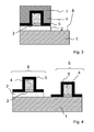
- the Figures 1 to 4 represent the various manufacturing steps of a CMOS comprising at least one PMOS transistor and at least one NMOS transistor.
- the figure 1 illustrates a PMOS transistor 6 on a silicon-germanium layer 2.
- the figure 2 illustrates the protection of PMOS transistors 6 of the figure 1 by a resin layer 7 for the manufacture of at least one NMOS transistor 9.
- the spacer 5 and the resin 7 having been removed on the zones 8 where the germanium silicon layer 2 will be withdrawn in order to form the transistor NMOS 9.
- the figure 3 illustrates a PMOS transistor 6 in which the germanium silicon layer 2 has been removed on the zones 8 intended to receive an NMOS transistor 9.
- the figure 4 illustrates a PMOS transistor 6 and an NMOS transistor 9 formed on the same substrate 1.
- the device preferably comprises a silicon 1 or silicon on insulator (Silicon On Insulator) substrate plate.
- a germanium silicon layer 2 is deposited on the silicon substrate 1.
- the silicon-germanium 2 preferentially forms the channel of the PMOS transistor 6.
- the PMOS transistor 6 comprises a gate 4, for example made of poly silicon or metal, surrounded by and others of spacers 5, for example silicon oxide or silicon nitride. Between the gate 4 and the silicon-germanium layer 2 is a layer of silicon oxide 3 or a high permittivity material called "high k" such as HfO2, HfSiO, HfZrO2, Al2O3.
- the resin 2 is then removed at the zones 8 between the PMOS transistors 6.
- the silicon-germanium layer 2 at the zones 8 is exposed so as to allow its partial or total removal.
- NMOS transistor 9 It is in these areas 8 that the NMOS transistor 9 will be formed.
- the total removal of the silicon-germanium layer 2 at the zones 8 is preferred.
- an etching solution is used to remove the silicon-germanium layer 2.
- a pre-treatment solution can be applied before the removal of this silicon-germanium layer 2.
- a post-treatment solution can be applied after the removal of this silicon-germanium layer 2.
- the NMOS transistor 9 is formed on a silicon 1 or silicon on insulator (silicon on insulator) substrate and comprises a grid 4, for example made of poly silicon or metal, surrounded by and others of spacers. 5, for example in silicon oxide or silicon nitride. Between the gate 4 and the silicon-germanium layer 2 is a layer of silicon oxide 3 or a high permittivity material called "high k" such as HfO2, HfSiO, HfZrO2, Al2O3.
- high k high permittivity material
- the removal in at least some zones 8 of the silicon-germanium layer 2 in a transistor must have a high selectivity.
- the evolution of microelectronics tends in particular to reduce the size of the nodes between the transistors, current research aims to obtain nodes smaller than 30 nanometers.
- the SOI substrate 1 is generalized and in this case the upper silicon thickness is critical, the etching of the silicon-germanium layer 2 must be highly selective so as not to etch the silicon of the substrate 1. It is then essential that the sharpness of the shrinkage is maximal without damaging or weakly the resin 7.
- the etching solution is prepared by mixing hydrofluoric acid (HF), hydrogen peroxide (H 2 O 2 ), acetic acid (CH 3 COOH) and ammonia (NH 4). 4 OH).
- the etching solution has a pH greater than 3 and advantageously less than 6, advantageously between 3.5 and 4. In this pH range, it has been found that the resin mask 7 is not damaged by the etching solution and that the etching selectivity of the silicon-germanium layer 2 is satisfactory, especially with respect to the silicon substrate 1.
- the resin 7 used according to the invention is a photosensitive resin, for example a polymer of the PolyHydroStryréne (PHS) type.
- the resin 7 is deposited in a layer with a thickness of 100 to 200 nm.
- the etching solution is prepared with a ratio between the four initial components being 1/2/3/4 respectively of HF / H 2 O 2 / CH 3 COOH / NH 4 OH.
- Ammonia (NH 4 OH) in a larger quantity makes it possible to neutralize the acids namely hydrofluoric acid (HF) and acetic acid (CH 3 COOH).
- HF hydrofluoric acid
- CH 3 COOH acetic acid
- the solution thus formed is a buffered solution, it has the property of keeping its pH stable over a certain dilution range.
- the hydrofluoric acid (HF) used is 49% by mass percentage
- the ammonia comprises 28% of NH 4 OH in weight percent
- the acetic acid is 100% pure.
- the dilution is advantageously carried out with deionized water.
- the dilution of the solution is preferably between 5 and 500 times, preferably 20 to 100 times.
- Dilution of the solution helps to reduce exothermicity when mixing the four components (see Examples 3 and 4).
- the decrease in temperature makes it possible in particular to control the etching rate and to improve the homogeneity of the etching on the entire plate by limiting the differences between the edge zones and the central zones.
- the low exothermicity of the etching solution during its manufacture allows almost simultaneous use. It is not necessary to provide a waiting period between the preparation of the etching solution and its use.
- the etching solution can be manufactured dynamically by directly injecting the four components and the deionized water simultaneously and independently unmixed or in advance where the mixture of the four components is prepared beforehand and then injected .
- the method according to the invention allows a selectivity of the step of removing the silicon-germanium layer 2 from the silicon layer 1 of between 4/1 and 50/1 for germanium silicon layers ranging from 5 to 60% germanium, preferably 10 to 60%.
- Selectivity refers to the ratio of the thicknesses of the different layers measured by the etching solution or the ratio of the etching rates of the different materials by the etching solution.
- An etching solution is prepared according to the following information without dilution: HF / H2O2 / CH3COOH / NH4O in 1/2/3/4 ratios without the addition of deionized water for dilution.
- V (H20) cc V (H202) cc V (dilution) cc 0 20 20 % HF V (HF) cc d (HF) n (HF) mol 49 10 1.19 0.2916 % NH40H V (NH40H) cc d (NH40H) n (NH40H) mol 28 40 0.895 .2860 % CH3COOH V (CH3COOH) cc d (CH 3 COOH) n (CH3COOH) mol 100 30 1,045 .5221
- An etching solution is prepared according to the information below with dilution: HF / H2O2 / CH3COOH / NH4OH in ratios of 1/2/3/4 with a dilution in 400cc of deionized water.
- the dilution is 5 times for a ratio that can be defined as 1/2/3/4/40.
- the etching solution is a buffered solution. Dilutions make it possible to adapt the etching rates without substantially modifying the pH of the solution, the latter being buffered.
- etching solution is prepared according to the amounts below. The concentrations of the various components are close to those of Example 1. v (HF) V (H2O2) v (CH3COOH) v (NH4OH) v (DI) Vtotal pH 10 20 30 40 100 200 4.03
- the etching solution thus prepared is used on: a layer of 28 nm of silicon-germanium (SiGe) at 30%, a layer of 74 nm of silicon-germanium (SiGe) at 20%, a layer of 45 nm of silicon (Si). Exposure time T ° C Thickness removed 2 min 50 All layers are removed
- the etching solution has a high exothermicity. Since the etching rate is too high, the selectivity of the solution can not be calculated.
- the thickness measurements of the layers are made by ellipsometry.
- etching solution is prepared according to the amounts below.
- concentrations of the different components are close to those of the example v (HF) V (H2O2) v (CH3COOH) v (NH4OH) v (DI) Vtotal pH 10 20 30 40 400 500 3.95
- the etching solution thus prepared is used on: a layer of 28 nm of silicon-germanium (SiGe) at 30%, a layer of 74 nm of silicon-germanium (SiGe) at 20%, a layer of 45 nm of silicon (Si). Exposure time T ° C Thickness removed 1 min 35 2.9nm of Si for 12nm of SiGe at 20%
- the thickness removed from the silicon and silicon-germanium layers is controlled.
- the etching solution contains components forming oxidizing species namely hydrogen peroxide (H2O2) and acetic acid (CH3COOH) which form per acetic acid (CH3CO3H) with high oxidizing power.
- H2O2 hydrogen peroxide
- CH3COOH acetic acid
- the etching solution also contains components forming etching species, namely hydrofluoric acid (HF) and ammonia (NH4OH), which form species with a high etching power.
- etching species namely hydrofluoric acid (HF) and ammonia (NH4OH), which form species with a high etching power.
- ammonia increases the pH of the etching solution and removes it from an efficient etching but ammonia (NH4OH) reacts notably with hydrofluoric acid (HF) to form ammonium fluoride (NH4F) in the ammonium ion / fluoride ion (NH4 + / F-) form which contributes to the etching of the silicon germanium by the formation of hydrogen difluoride (HF2-) between the hydrofluoric acid (HF) and the fluoride ion (F- ).
- HF2- hydrogen difluoride
- the oxidation and etching phenomena succeed one another in a repetitive manner.
- the removal step has a duration of between 20 and 600 seconds depending on the etching rate of the solution and the thickness of the layer that is to be removed. Preferably, it lasts from 30 to 120 seconds, advantageously of the order of 60 seconds.
- the method of manufacturing the semiconductor device also comprises at least one pre-treatment step.
- This pre-treatment step is performed before the withdrawal step. It consists in exposing the zones 8 of the silicon-germanium layer 2 (SiGe) to be removed to a pretreatment solution.
- the resin layer 7 is preferably already in place.
- the pretreatment solution is therefore advantageously compatible with the resin layer 7.
- This pretreatment step advantageously makes it possible to eliminate any contaminants on the surface of the layer of silicon germanium 2 to remove. Among the contaminants, traces of silicon oxides are removed by the pretreatment solution. Indeed, it is preferred that the silicon-germanium layer 2 (SiGe) is not contaminated or oxidized before the removal step. Otherwise, during the removal step, the etching does not begin simultaneously over the entire surface of the areas to be removed, so a non-homogeneous shrinkage is obtained.
- the duration of the exposure of the pretreatment stage is from 20 to 300 seconds, preferably from 30 to 120 seconds, advantageously of the order of 40 seconds.
- the pretreatment solution has a pH of preferably between 3 and 5, advantageously of the order of 3. It advantageously contains hydrofluoric acid (HF).
- the pretreatment solution advantageously has a ratio of NH4F / HF ranging from 2/1 to 500/1, preferentially from 2/1 to 30/1, more preferably from 2/1 to 6/1.
- the pretreatment solution is formed from hydrofluoric acid (HF) and ammonia (NH4OH).
- the solvent is typically deionized water.
- the reaction is almost complete between these two species to form an ammonium fluoride salt (NH4F).
- the hydrofluoric acid (HF) is in excess, the reaction is limited by the amount of ammonia (NH 4 OH) initially introduced so that the final equilibrium solution corresponds to a mixture of hydrofluoric acid (HF) and fluoride ammonium (NH4F).
- the solution is buffered. This manufacturing method makes it possible to obtain a solution with a pH compatible with a resin mask as well as to allow large dilutions while maintaining a suitable pH.
- the solution is diluted 5 and 100 times, preferably about 50 times.
- the ammonium fluoride salt (NH4F) is advantageously in a dissolved form (NH4 + / F-).
- the method comprises at least one post-processing step.
- This post-processing step is performed after the removal step. It consists of exposing the zones 8 of the silicon-germanium layer 2 (SiGe) which have been totally or partially removed during the removal step to a post-treatment solution. This step helps to remove any contaminants left on the surface of said zones at the end of the withdrawal step. Among these contaminants, there are oxides of silicon, silicon-germanium and / or the remaining components of the etching solution.
- This step consists of cleaning said zones 8 of sorts to allow a new withdrawal step, as described above, or a layer growth step.
- the duration of the exposure of the post-treatment step is between 10 and 180 seconds, preferably from 20 to 60 seconds and advantageously of the order of 20 seconds.
- the post-treatment solution is preferably identical to the pretreatment solution described above.
- the method comprises in the order a pretreatment step, a withdrawal step and a post-processing step. It may be advantageous to provide for several of these steps.
- the method comprises in the order a pretreatment step, a withdrawal step, a post-processing step, a withdrawal step and a post-processing step.
- the number of withdrawal steps and therefore pre and post-treatment steps depends on the thickness and the number of layers to be removed.
- the method comprises a pretreatment step of a duration of the order of 30 to 90 seconds, preferably of the order of 60 seconds, a step of withdrawal of a duration of the order of 30 to 180 seconds. seconds preferably of the order of 60 to 120 seconds and a post-processing step of a duration of the order of 20 to 90 seconds preferably of the order of 20 to 60 seconds.
- the ratio of ammonia fluoride (NH4F) / hydrofluoric acid (HF) is 3/1 for a pH of 3.48.
- the pretreatment, withdrawal and post-treatment steps are carried out successively with respective durations of 60 seconds on the following samples: either silicon or layers of silicon germanium at different concentrations: 28 nm SiGe 30% - 53 nmSiGe 10% - 75nm SiGe 20% - 40nm SiGe 40% - 26nm SiGe 50%.
- the removal of the silicon layer is of the order of 0.9 nm while the removal of the silicon-germanium layer at 10% is of the order of 1.2 nm. A 30% silicon-germanium layer is completely removed, ie 28 nm.
- a selectivity of the order of 30/1 is obtained for the 30% germanium silicon layer.
- the etching rate is 120 Angstrom / minute or 12 nm for 30% silicon germanium.
- the etching rate can be decreased if it is desired not to remove the entire silicon germanium layer. Otherwise, the burn time is reduced to limit the shrinkage.
Landscapes
- Weting (AREA)
- Chemical & Material Sciences (AREA)
- Chemical Kinetics & Catalysis (AREA)
- General Chemical & Material Sciences (AREA)
- Cleaning Or Drying Semiconductors (AREA)
Abstract
La présente invention concerne un procédé de fabrication d'un dispositif semi conducteur par gravure chimique par voie humide le dispositif comprenant au moins une couche de silicium (Si) et au moins une couche de silicium-germanium (SiGe) et au moins une couche de résine photosensible formant un masque recouvrant en partie la couche de silicium germanium (SiGe) et laissant libre la couche de silicium germanium en certaines zones caractérisé en ce qu'il comprend une étape de fabrication d'une solution de gravure, ayant un pH compris entre 3 et 6, à partir d'acide hydrofluorique (HF), de peroxyde d'hydrogène (H 2 O 2 ), d'acide acétique (CH 3 COOH) et d'ammoniaque (NH 4 OH) et une étape de retrait de la couche de silicium-germanium (SiGe) au moins niveau desdites zones par exposition à ladite solution de gravure. L'invention trouvera son application pour la fabrication de circuits intégrés et plus précisément de transistors. Notamment, pour l'optimisation des transistors CMOS de dernière génération.The present invention relates to a method for manufacturing a semiconductor device by wet chemical etching the device comprising at least one silicon layer (Si) and at least one layer of silicon-germanium (SiGe) and at least one layer of photoresist forming a mask partially covering the layer of silicon germanium (SiGe) and leaving free the layer of silicon germanium in certain areas characterized in that it comprises a step of manufacturing an etching solution, having a pH between 3 and 6, from hydrofluoric acid (HF), hydrogen peroxide (H 2 O 2), acetic acid (CH 3 COOH) and ammonia (NH 4 OH) and a step of removing the silicon-germanium (SiGe) layer at least one of said zones by exposure to said etching solution. The invention will find its application for the manufacture of integrated circuits and more specifically of transistors. In particular, for the optimization of the latest-generation CMOS transistors.
Description
La présente invention concerne un procédé de fabrication d'un dispositif semi-conducteur avec une étape de retrait sélective d'une couche de silicium-germanium.The present invention relates to a method of manufacturing a semiconductor device with a step of selective removal of a silicon-germanium layer.
L'invention trouvera son application pour la fabrication de circuits intégrés et plus précisément de transistors. Notamment, pour l'optimisation des transistors CMOS (Semi-conducteur à oxyde de métal complémentaire ou Complementary Metal Oxide Semiconductor en anglais) de dernière génération, il est intéressant de prévoir un canal en silicium-germanium (SiGe) pour la partie PMOS (Semi-conducteur à oxyde de métal à canal positif ou Positive Metal Oxide Semiconductor en anglais). Toutefois, cette couche n'a pas d'intérêt pour un transistor NMOS (Semi-conducteur à oxyde de métal à canal négatif ou Negative Metal Oxide Semi-conductor en anglais). La fabrication de ces deux types de transistor PMOS et NMOS, peut être associée. Un transistor PMOS est dans un premier temps réalisé sur une couche de silicium-germanium puis le NMOS est préparé. Pour cela, le PMOS est masqué par une couche de résine de sorte à être protégé. Puis, il faut éliminer localement le silicium-germanium, à travers le masque de résine dans les zones destinées à recevoir un NMOS. Ce retrait du silicium-germanium doit être sélectif vis-à-vis des couches inferieures et de la résine.The invention will find its application for the manufacture of integrated circuits and more specifically of transistors. In particular, for the optimization of CMOS transistors (complementary metal oxide semiconductor or Complementary Metal Oxide Semiconductor), it is interesting to provide a silicon-germanium (SiGe) channel for the PMOS part (Semi Positive Metal Oxide Semiconductor or Positive Metal Oxide Semiconductor). However, this layer is not of interest for an NMOS transistor (Negative Metal Oxide Semiconductor or Negative Metal Oxide semiconductor). The manufacture of these two types of PMOS and NMOS transistor can be associated. A PMOS transistor is first made on a silicon-germanium layer and then the NMOS is prepared. For this, the PMOS is masked by a layer of resin so as to be protected. Then, silicon-germanium must be removed locally, through the resin mask in the areas to receive an NMOS. This removal of the silicon-germanium must be selective with respect to the lower layers and the resin.
On connaît pour cela de la gravure sèche au plasma. Malgré une sélectivité intéressante, le coût de cette technologie ne permet pas son utilisation à grande échelle.This is known for dry plasma etching. Despite an interesting selectivity, the cost of this technology does not allow its use on a large scale.
Un traitement à base d'acide chlorhydrique gazeux (HCl) peut également être réalisé dans un réacteur. Cette technique n'est pas applicable à tous les transistors car la sélectivité varie grandement en fonction du pourcentage de germanium dans la couche de silicium-germanium à éliminer.A treatment based on gaseous hydrochloric acid (HCl) can also be carried out in a reactor. This technique is not applicable to all transistors because the selectivity varies greatly depending on the percentage of germanium in the silicon-germanium layer to be removed.
Des essais de gravure par voie humide ont été faits avec des solutions d'acide fluorhydrique (HF), de peroxyde d'hydrogène (H2O2) et d'acide acétique (CH3COOH).Wet etching tests were made with solutions of hydrofluoric acid (HF), hydrogen peroxide (H 2 O 2 ) and acetic acid (CH 3 COOH).
La gravure par voie humide n'est pas satisfaisante pour éliminer une couche de silicium-germanium, notamment en présence d'un masque de résine.Wet etching is not satisfactory for removing a layer of silicon-germanium, especially in the presence of a resin mask.
En effet, il s'est avéré que ce type de solution attaque une partie de la résine. Les flancs des motifs formés dans la résine sont notamment endommagés. La dimension des motifs est par conséquent peu maitrisée.Indeed, it turned out that this type of solution attacks part of the resin. The flanks of the patterns formed in the resin are particularly damaged. The size of the patterns is therefore little controlled.
Il existe donc le besoin de proposer un procédé pour éliminer une couche de silicium-germanium par voie humide et préférentiellement avec une sélectivité satisfaisante et sans endommager significativement un masque de résine.There is therefore the need to provide a method for removing a silicon-germanium layer wet and preferably with a satisfactory selectivity and without significantly damaging a resin mask.
A cet effet, la présente invention concerne un procédé de fabrication d'un dispositif semi conducteur par gravure chimique par voie humide, le dispositif comprenant au moins une couche de silicium (Si) et au moins une couche de silicium-germanium (SiGe) et au moins une couche de résine photosensible formant un masque recouvrant en partie la couche de silicium germanium (SiGe) et laissant libre la couche de silicium germanium en certaines zones caractérisé en ce qu'il comprend une étape de retrait de la couche de silicium-germanium (SiGe) au moins au niveau desdites zones par exposition à une solution de gravure. La solution de gravure ayant un pH compris entre 3 et 6, est avantageusement formée par une étape de fabrication à partir d'acide hydrofluorique (HF), de peroxyde d'hydrogène (H2O2), d'acide acétique (CH3COOH) et d'ammoniaque (NH4OH).For this purpose, the present invention relates to a method of manufacturing a semiconductor device by wet chemical etching, the device comprising at least one silicon layer (Si) and at least one silicon-germanium layer (SiGe) and at least one layer of photosensitive resin forming a mask partially covering the layer of silicon germanium (SiGe) and leaving free the layer of silicon germanium in certain zones characterized in that it comprises a step of removing the silicon-germanium (SiGe) layer at least at said zones by exposure to an etching solution. The etching solution having a pH of between 3 and 6 is advantageously formed by a manufacturing step from hydrofluoric acid (HF), hydrogen peroxide (H 2 O 2 ), acetic acid (CH 3 COOH) and ammonia (NH 4 OH).
La combinaison de ces quatre composants dans la solution de gravure permet d'obtenir une étape de retrait préférentiellement sélective de la couche de silicium germanium. Le pH de la solution de gravure est étudié à la fois pour être compatible avec un masque de résine et à la fois pour permettre un retrait sélectif de la couche de silicium germanium. En effet, pour un homme de l'art ces objectifs semblent, a priori, opposés ; le pH pour ne pas endommager une résine, se situe avantageusement aux alentours de 3 à 6 alors que pour obtenir un retrait sélectif, la quantité d'espèces gravantes doit être maximale soit autour d'un pH de 1 à 2.The combination of these four components in the etching solution makes it possible to obtain a preferentially selective removal step of the germanium silicon layer. The pH of the etching solution is studied both to be compatible with a resin mask and both to allow selective removal of the silicon germanium layer. Indeed, for a man of the art these objectives seem, a priori, opposite; the pH not to damage a resin, is advantageously around 3 to 6 while to obtain a selective shrinkage, the amount of etching species must be maximum or around a pH of 1 to 2.
Selon l'invention, l'ajout d'ammoniaque (NH4OH) à une solution contenant de l'acide hydrofluorique (HF) n'est habituellement pas envisagé puisque ce mélange entraine facilement la formation d'un sel de fluorure d'ammonium (NH4F). La présence de ce sel entraine une défectivité sur la plaque de semi-conducteur, mais aussi des endommagements dans l'équipement en bloquant des conduits...According to the invention, the addition of ammonia (NH 4 OH) to a solution containing hydrofluoric acid (HF) is not usually envisaged since this mixture easily leads to the formation of an ammonium fluoride salt (NH 4 F). The presence of this salt causes a defect on the semiconductor plate, but also damages in the equipment by blocking conduits.
De plus, le mélange d'acide-base dans une telle solution de gravure génère couramment une forte exothermicité qui crée des problèmes de non uniformité de la gravure. En outre, plus une solution de gravure comporte de composés, plus les problèmes liés à l'uniformité de la gravure sont amplifiés.In addition, the mixture of acid-base in such an etching solution commonly generates a strong exothermicity which creates problems of nonuniformity of etching. In addition, the more compounding a solution of etching, the more the problems related to the uniformity of the etching are amplified.
Selon l'invention ces inconvénients sont au moins en partie levés par le présent procédé et sa solution de gravure.According to the invention these disadvantages are at least partially overcome by the present method and its etching solution.
Préférentiellement, la solution de gravure selon l'invention est diluée entre 5 et 500 fois. Cette dilution apporte de nombreux avantages dont un contrôle de la vitesse de gravure et une meilleure gravure. Le facteur de dilution est calculé par rapport au volume total de la solution de gravure avant dilution.Preferably, the etching solution according to the invention is diluted between 5 and 500 times. This dilution brings many benefits including control of etching speed and better etching. The dilution factor is calculated based on the total volume of the etching solution before dilution.
Le procédé selon l'invention permet un retrait des zones de silicium-germanium avec une très bonne sélectivité vis-à-vis des autres couches du transistor et sans endommager, ou peu, le masque de résine.The method according to the invention allows a removal of the silicon-germanium zones with a very good selectivity vis-à-vis the other layers of the transistor and without damaging, or little, the resin mask.
Selon une possibilité préférée, le procédé comprend au moins une étape de pré traitement et/ou une étape de post traitement respectivement avant et après l'étape de retrait.According to a preferred possibility, the method comprises at least one pre-treatment step and / or one post-treatment step respectively before and after the withdrawal step.
Il est très avantageux de prévoir au moins une étape préliminaire de traitement, étape de pré traitement, facilitant ensuite le démarrage de l'étape de retrait. De même, l'étape de post traitement améliore avantageusement l'état de surface de la couche située sous les zones de retrait en retirant des éventuels contaminants, plus particulièrement de l'oxyde de silicium dans le cas d'un retrait total de la couche de silicium-germanium sur une zone, ou d'oxyde de silicium-germanium dans le cas d'un retrait partiel. Cette étape post traitement facilite les étapes suivantes éventuelles de retrait de couches et/ou de croissance.It is very advantageous to provide at least one preliminary stage of treatment, pre-treatment step, then facilitating the start of the withdrawal step. Likewise, the post-treatment step advantageously improves the surface state of the layer beneath the shrinkage zones by removing any contaminants, more particularly silicon oxide, in the case of a total withdrawal of the layer. silicon-germanium on a zone, or silicon-germanium oxide in the case of a partial withdrawal. This post-treatment step facilitates the possible subsequent steps of layer removal and / or growth.
Préférentiellement, les solutions utilisées pour l'étape de pré traitement et l'étape de post traitement sont fabriquées par mélange d'acide fluorhydrique (HCl) et d'ammoniaque (NH4OH).Preferentially, the solutions used for the pre-treatment stage and the post-treatment stage are manufactured by mixing hydrofluoric acid (HCl) and ammonia (NH 4 OH).
Ce procédé de préparation amène à une solution tamponnée ayant un pH conforme à une utilisation avec un masque de résine, soit préférentiellement de 3 à 6 et avantageusement à une sélectivité envers le silicium-germanium.This preparation method leads to a buffered solution having a pH in accordance with use with a resin mask, preferably from 3 to 6 and advantageously to selectivity towards silicon-germanium.
Suivant des variantes préférées cumulatives ou alternatives de l'invention, le procédé est tel que :
- le pH de la solution de gravure est compris entre 3 et 6 préférentiellement 3.5 et 4,
- la fabrication de la solution de gravure est réalisée à partir d'acide hydrofluorique (HF), de peroxyde d'hydrogène (H2O2), d'acide acétique (CH3COOH) et d'ammoniaque (NH4OH) dans des ratios respectifs de 1/2/3/4,
- la solution de gravure est diluée dans de l'eau déionisée entre 5 et 500 fois,
- la durée de l'exposition à la solution de gravure est comprise entre 20 secondes à 600 secondes,
- la durée de l'exposition à la solution de gravure est comprise entre 30 secondes à 120 secondes,
- il comprend avant l'étape de retrait une étape de prétraitement comprenant une exposition au moins desdites zones de la couche de silicium-germanium (SiGe) à une solution de prétraitement,
- il comprend une étape de fabrication d'une solution de prétraitement à partir d'acide hydrofluorique (HF) et d'ammoniaque (NH4OH), préférentiellement dans un ratio NH4F/HF de 2/1 à 6/1,
- la durée de l'exposition à la solution de prétraitement est comprise entre 20 secondes et 300 secondes,
- la durée de l'exposition à la solution de pré traitement est comprise entre 30 secondes et 120 secondes,
- il comprend après l'étape de retrait une étape de post traitement par exposition au moins desdites zones de la couche de silicium-germanium (SiGe) à une solution de post-traitement,
- il comprend une étape de fabrication d'une solution de post-traitement à partir d'acide hydrofluorique (HF) et d'ammoniaque (NH4OH), préférentiellement dans un ratio NH4F/HF de 2/1 à 6/1,
- la durée de l'exposition à la solution de post-traitement est comprise entre 10 secondes et 180 secondes,
- la durée de l'exposition à la solution de post traitement est comprise entre 20 secondes à 60 secondes,
- la couche de silicium-germanium (SiGe) contient un pourcentage de germanium allant de 5 à 60%,
- la couche de silicium-germanium (SiGe) forme un canal d'un transistor,
- l'étape de retrait de la couche de silicium-germanium (SiGe) est opérée de sorte à complètement retirer ladite couche de silicium-germanium (SiGe) sur lesdites zones, la couche de silicium (Si) étant mise à nu dans ces zones,
- the pH of the etching solution is between 3 and 6, preferably 3.5 and 4,
- the etching solution is manufactured from hydrofluoric acid (HF), hydrogen peroxide (H 2 O 2 ), acetic acid (CH 3 COOH) and ammonia (NH 4 OH) in respective ratios of 1/2/3/4,
- the etching solution is diluted in deionized water between 5 and 500 times,
- the duration of exposure to the etching solution is between 20 seconds to 600 seconds,
- the duration of exposure to the etching solution is between 30 seconds to 120 seconds,
- it comprises before the removal step a pretreatment step comprising exposing at least said zones of the silicon-germanium (SiGe) layer to a pretreatment solution,
- it comprises a step of manufacturing a pretreatment solution from hydrofluoric acid (HF) and ammonia (NH 4 OH), preferably in an NH 4 F / HF ratio of 2/1 to 6/1,
- the duration of the exposure to the pretreatment solution is between 20 seconds and 300 seconds,
- the duration of the exposure to the pre-treatment solution is between 30 seconds and 120 seconds,
- it comprises after the removal step a post-treatment step by exposing at least said zones of the silicon-germanium (SiGe) layer to a post-treatment solution,
- it comprises a step of manufacturing a post-treatment solution from hydrofluoric acid (HF) and ammonia (NH 4 OH), preferably in an NH 4 F / HF ratio of 2/1 to 6/1,
- the duration of exposure to the post-treatment solution is between 10 seconds and 180 seconds,
- the duration of exposure to the post-treatment solution is between 20 seconds to 60 seconds,
- the silicon-germanium (SiGe) layer contains a percentage of germanium ranging from 5 to 60%,
- the silicon-germanium (SiGe) layer forms a channel of a transistor,
- the step of removing the silicon-germanium (SiGe) layer is carried out so as to completely remove said silicon-germanium (SiGe) layer on said zones, the silicon layer (Si) being exposed in these zones,
L'invention concerne également une composition dans laquelle l'acide hydrofluorique (HF), le peroxyde d'hydrogène (H2O2), l'acide acétique (CH3COOH) et l'ammoniaque (NH4OH) sont mélangés dans des proportions de 1/2/3/4.The invention also relates to a composition in which hydrofluoric acid (HF), hydrogen peroxide (H 2 O 2 ), acetic acid (CH 3 COOH) and ammonia (NH 4 OH) are mixed in. proportions of 1/2/3/4.
Avantageusement, la composition selon l'invention comprend un pH compris entre 3 à 6.Advantageously, the composition according to the invention comprises a pH of between 3 and 6.
Avantageusement, la composition selon l'invention est diluée dans de l'eau déionisée de 5 à 500 fois.Advantageously, the composition according to the invention is diluted in
Le dispositif semi conducteur fabriqué par le présent procédé comprend au moins un transistor.The semiconductor device manufactured by the present method comprises at least one transistor.
Les dessins ci-joints sont donnés à titre d'exemple et ne sont pas limitatifs de l'invention. Ils représentent seulement un mode de réalisation de l'invention et permettront de la comprendre aisément.The accompanying drawings are given by way of example and are not limiting of the invention. They represent only one embodiment of the invention and will make it easy to understand.
Les
La
La
La
La
Le dispositif comprend préférentiellement une plaque de substrat en silicium 1 ou silicium sur isolant (Silicium On Insulator en anglais - SOI).The device preferably comprises a
Pour former un transistor PMOS 6, une couche de silicium germanium 2 est déposée sur le substrat en silicium 1. Le silicium-germanium 2 forme préférentiellement le canal du transistor PMOS 6.To form a
Le transistor PMOS 6 comprend une grille 4, par exemple en poly silicium ou en métal, entourée de par et d'autres d'espaceurs 5, par exemple en oxyde de silicium ou en nitrure de silicium. Entre la grille 4 et la couche de silicium-germanium 2, se trouve une couche d'oxyde de silicium 3 ou un matériau à forte permittivité appelé «high k» comme par exemple HfO2, HfSiO, HfZr02, Al2O3.The
Une fois, le (ou les) transistor PMOS 6 formé sur la couche de silicium-germanium 2, une couche de résine 7, préférentiellement photosensible, est disposée pour recouvrir totalement le transistor PMOS. La résine 2 est ensuite retirée au niveau des zones 8 entre les transistors PMOS 6. La couche de silicium-germanium 2 au niveau des zones 8 est mise à nu de sorte à permettre son retrait partiel ou total.Once, the (or)
C'est dans ces zones 8 que le transistor NMOS 9 va être formé. Pour la formation d'un transistor NMOS 6, le retrait total de la couche de silicium-germanium 2 au niveau des zones 8 est préféré.It is in these
Selon l'invention, une solution de gravure est utilisée pour retirer la couche de silicium-germanium 2. Préférentiellement, avant le retrait de cette couche de silicium-germanium 2, une solution de pré traitement peut être appliquée. Préférentiellement, après le retrait de cette couche de silicium-germanium 2, une solution de post traitement peut être appliquée.According to the invention, an etching solution is used to remove the silicon-
Le transistor NMOS 9 est formé sur un substrat en silicium 1 ou silicium sur isolant (Silicium On Insulator en anglais - SOI) et comprend une grille 4, par exemple en poly silicium ou en métal, entourée de par et d'autres d'espaceurs 5, par exemple en oxyde de silicium ou en nitrure de silicium. Entre la grille 4 et la couche de silicium-germanium 2, se trouve une couche d'oxyde de silicium 3 ou un matériau à forte permittivité appelé «high k» comme par exemple HfO2, HfSiO, HfZr02, Al2O3..The
On entend par « sur » que les couches sont directement en contact mais aussi que la couche recouvre, avec éventuellement une couche intermédiaire.By "on" is meant that the layers are directly in contact but also that the layer covers, possibly with an intermediate layer.
Le retrait en au moins certaines zones 8 de la couche de silicium-germanium 2 dans un transistor doit présenter une sélectivité importante. L'évolution de la microélectronique tend notamment à réduire les dimensions des noeuds entre les transistors, les recherches actuelles visent à obtenir des noeuds inférieurs à 30 nanomètres. De plus, le substrat 1 en SOI se généralise et dans ce cas là l'épaisseur supérieure de silicium est critique, la gravure de la couche de silicium germanium 2 doit être hautement sélective pour ne pas graver le silicium du substrat 1. Il est alors essentiel que la netteté du retrait soit maximale sans endommager ou très faiblement la résine 7.The removal in at least some
Selon l'invention la solution de gravure est préparée en mélangeant de l'acide fluorhydrique (HF), du peroxyde d'hydrogène (H2O2), de l'acide acétique (CH3COOH) et de l'ammoniaque (NH4OH).According to the invention, the etching solution is prepared by mixing hydrofluoric acid (HF), hydrogen peroxide (H 2 O 2 ), acetic acid (CH 3 COOH) and ammonia (NH 4). 4 OH).
Préférentiellement, la solution de gravure possède un pH supérieur à 3 et avantageusement inférieur à 6, avantageusement entre 3,5 et 4. Dans cette gamme de pH, il a pu être constaté que le masque de résine 7 n'est pas endommagé par la solution de gravure et que la sélectivité de gravure de la couche de silicium germanium 2 est satisfaisante, notamment vis-à-vis du substrat en silicium 1.Preferably, the etching solution has a pH greater than 3 and advantageously less than 6, advantageously between 3.5 and 4. In this pH range, it has been found that the
A titre préféré, la résine 7 mise en oeuvre selon l'invention est une résine photosensitive, par exemple en polymère de type PolyHydroStryréne (PHS). Avantageusement, la résine 7 est déposée en une couche d'une épaisseur de 100 à 200nm.By way of preference, the
Les proportions des quatre composants initiaux de la solution de gravure sont étudiées. Préférentiellement, la solution de gravure est préparée avec un rapport entre les quatre composants initiaux étant 1/2/3/4 respectivement de HF/H2O2/CH3COOH/NH4OH. L'ammoniaque (NH4OH) en quantité plus importante permet de neutraliser les acides à savoir l'acide fluorhydrique (HF) et l'acide acétique (CH3COOH). Il y a une augmentation de pH. La solution ainsi formée est une solution tamponnée, elle a la propriété de conserver son pH stable sur une certaine gamme de dilution.The proportions of the four initial components of the etching solution are studied. Preferably, the etching solution is prepared with a ratio between the four initial components being 1/2/3/4 respectively of HF / H 2 O 2 / CH 3 COOH / NH 4 OH. Ammonia (NH 4 OH) in a larger quantity makes it possible to neutralize the acids namely hydrofluoric acid (HF) and acetic acid (CH 3 COOH). There is an increase in pH. The solution thus formed is a buffered solution, it has the property of keeping its pH stable over a certain dilution range.
Préférentiellement, l'acide hydrofluorique (HF) utilisé est à 49% en pourcentage massique, l'ammoniaque comprend 28% de NH4OH en pourcentage massique et l'acide acétique est pur à 100%.Preferably, the hydrofluoric acid (HF) used is 49% by mass percentage, the ammonia comprises 28% of NH 4 OH in weight percent and the acetic acid is 100% pure.
Il est préféré de diluer la solution de gravure. La dilution est avantageusement réalisée par de l'eau déionisée. La dilution de la solution est préférentiellement comprise entre 5 et 500 fois, préférentiellement de 20 à 100 fois.It is preferred to dilute the etching solution. The dilution is advantageously carried out with deionized water. The dilution of the solution is preferably between 5 and 500 times, preferably 20 to 100 times.
La dilution de la solution contribue à atténuer l'exothermicité lors du mélange des quatre composants (confère exemples 3 et 4). La diminution de la température permet notamment de contrôler la vitesse de gravure et d'améliorer l'homogénéité de la gravure sur l'ensemble de la plaque en limitant les différences entre les zones de bordures et les zones centrales.Dilution of the solution helps to reduce exothermicity when mixing the four components (see Examples 3 and 4). The decrease in temperature makes it possible in particular to control the etching rate and to improve the homogeneity of the etching on the entire plate by limiting the differences between the edge zones and the central zones.
La faible exothermicité de la solution de gravure lors de sa fabrication permet une utilisation quasi simultanée. Il n'est pas nécessaire de prévoir un délai d'attente entre la préparation de la solution de gravure et son utilisation.The low exothermicity of the etching solution during its manufacture allows almost simultaneous use. It is not necessary to provide a waiting period between the preparation of the etching solution and its use.
Selon l'invention, la solution de gravure peut être fabriquée de manière dynamique en injectant directement les quatre composants et l'eau déionisée simultanément et de manière indépendante non mélangé ou bien de manière anticipée où le mélange des quatre composants est préparé au préalable puis injecté.According to the invention, the etching solution can be manufactured dynamically by directly injecting the four components and the deionized water simultaneously and independently unmixed or in advance where the mixture of the four components is prepared beforehand and then injected .
Le procédé selon l'invention permet une sélectivité de l'étape de retrait de la couche de silicium germanium 2 vis-à-vis de la couche de silicium 1 comprise entre 4/1 et 50/1 pour des couches de silicium germanium allant de 5 à 60% de germanium, préférentiellement de 10 à 60%.The method according to the invention allows a selectivity of the step of removing the silicon-
La sélectivité s'entend du rapport des épaisseurs relevées des différentes couches par la solution de gravure ou bien le rapport des vitesses de gravure des différents matériaux par la solution de gravure.Selectivity refers to the ratio of the thicknesses of the different layers measured by the etching solution or the ratio of the etching rates of the different materials by the etching solution.
Une solution de gravure est préparée suivant les informations ci-dessous sans dilution : HF/H2O2/CH3COOH/NH4O dans des rapports de 1/2/3/4 sans addition d'eau déionisée pour la dilution.
Par simulation, les concentrations théoriques en moles/litre des différentes espèces chimiques présentes dans la solution de gravure sont les suivantes.
Une solution de gravure est préparée suivant les informations ci-dessous avec dilution : HF/H2O2/CH3COOH/NH4OH dans des rapports de 1/2/3/4 avec une dilution dans 400cc d'eau déionisée. La dilution est de 5 fois pour un ratio pouvant être défini comme 1/2/3/4/40.
Le pH et les concentrations théoriques des différentes espèces présentes dans la solution de gravure sont présentées dans le tableau ci-dessous.
Grâce au procédé de fabrication de la solution de gravure selon l'invention, la solution de gravure est une solution tamponnée. Les dilutions, permettent d'adapter les vitesses de gravure sans modification notable du pH de la solution, celle-ci étant tamponnée.Thanks to the method of manufacturing the etching solution according to the invention, the etching solution is a buffered solution. Dilutions make it possible to adapt the etching rates without substantially modifying the pH of the solution, the latter being buffered.
Une solution de gravure est préparée suivant les quantités ci-dessous. Les concentrations des différents composants sont proches de celles de l'exemple 1.
La solution de gravure ainsi préparée est utilisée sur :
- une couche de 28nm de silicium-germanium (SiGe) à 30%,
- une couche de 74nm de silicium-germanium (SiGe) à 20%,
- une couche de 45nm de silicium (Si).
a layer of 28 nm of silicon-germanium (SiGe) at 30%,
a layer of 74 nm of silicon-germanium (SiGe) at 20%,
a layer of 45 nm of silicon (Si).
La solution de gravure présente une exothermicité importante. La vitesse de gravure étant trop élevée la sélectivité de la solution ne peut pas être calculée.The etching solution has a high exothermicity. Since the etching rate is too high, the selectivity of the solution can not be calculated.
Les mesures d'épaisseurs des couches sont réalisées par ellipsométrie.The thickness measurements of the layers are made by ellipsometry.
Une solution de gravure est préparée suivant les quantités ci-dessous. Les concentrations des différents composants sont proches de celles de l'exemple
La solution de gravure ainsi préparée est utilisée sur :
- une couche de 28nm de silicium-germanium (SiGe) à 30%,
- une couche de 74nm de silicium-germanium (SiGe) à 20%,
- une couche de 45nm de silicium (Si).
a layer of 28 nm of silicon-germanium (SiGe) at 30%,
a layer of 74 nm of silicon-germanium (SiGe) at 20%,
a layer of 45 nm of silicon (Si).
On arrive avec cette solution à graver sélectivement la couche de silicium-germanium (SiGe) à 20% avec une sélectivité de l'ordre de 1/4 vis-à-vis du silicium (Si).With this solution, it is possible to selectively etch the silicon-germanium (SiGe) layer at 20% with a selectivity of about 1/4 with respect to silicon (Si).
En diminuant également la durée de l'exposition, on contrôle l'épaisseur retirée des couches de silicium et silicium-germanium.By also reducing the duration of the exposure, the thickness removed from the silicon and silicon-germanium layers is controlled.
Sans être liée à une théorie, cette sélectivité pourrait s'expliquer par le fait que la solution de gravure contient des composants formant des espèces oxydantes à savoir le peroxyde d'hydrogène (H2O2) et l'acide acétique (CH3COOH) qui forment de l'acide per acétique (CH3CO3H) à fort pouvoir oxydant.Without being linked to a theory, this selectivity could be explained by the fact that the etching solution contains components forming oxidizing species namely hydrogen peroxide (H2O2) and acetic acid (CH3COOH) which form per acetic acid (CH3CO3H) with high oxidizing power.
Une fois les quatre composants mélangés et à l'équilibre de la réaction, on retrouve dans la solution de gravure les espèces suivantes : ion hydronium (H3O+), acide hydrofluorique (HF), ion fluorure (F-), ion hydrogène difluoride (HF2-), ion ammonium (NH4+), ion hydroxyde (OH-).Once the four components are mixed and equilibrium of the reaction, we find in the etching solution the following species: hydronium ion (H3O +), hydrofluoric acid (HF), fluoride ion (F-), hydrogen ion difluoride (HF2) -), ammonium ion (NH4 +), hydroxide ion (OH-).
La solution de gravure contient également des composants formant des espèces gravantes à savoir l'acide fluorhydrique (HF) et l'ammoniaque (NH4OH) qui forment des espèces présentant un haut pouvoir gravant.The etching solution also contains components forming etching species, namely hydrofluoric acid (HF) and ammonia (NH4OH), which form species with a high etching power.
L'ajout d'ammoniaque (NH4OH) augmente le pH de la solution de gravure et l'éloigne d'une gravure efficace mais l'ammoniaque (NH4OH) réagit notamment avec l'acide fluorhydrique (HF) pour former du fluorure d'ammonium (NH4F) sous forme ion ammonium/ ion fluorure (NH4+/F-) qui contribue à la gravure du silicium germanium par formation d'hydrogène difluoride (HF2-) entre l'acide fluorhydrique (HF) et l'ion fluorure (F-).The addition of ammonia (NH4OH) increases the pH of the etching solution and removes it from an efficient etching but ammonia (NH4OH) reacts notably with hydrofluoric acid (HF) to form ammonium fluoride (NH4F) in the ammonium ion / fluoride ion (NH4 + / F-) form which contributes to the etching of the silicon germanium by the formation of hydrogen difluoride (HF2-) between the hydrofluoric acid (HF) and the fluoride ion (F- ).
Lors de l'étape de retrait, les phénomènes d'oxydation et de gravure se succèdent de manière répétitive.During the removal step, the oxidation and etching phenomena succeed one another in a repetitive manner.
L'étape de retrait a une durée comprise entre 20 et 600 secondes en fonction de la vitesse de gravure de la solution et de l'épaisseur de la couche que l'on souhaite retirer. Préférentiellement, elle dure de 30 à 120 secondes, avantageusement de l'ordre de 60 secondes.The removal step has a duration of between 20 and 600 seconds depending on the etching rate of the solution and the thickness of the layer that is to be removed. Preferably, it lasts from 30 to 120 seconds, advantageously of the order of 60 seconds.
Selon un mode de réalisation préféré de l'invention, le procédé de fabrication du dispositif semi-conducteur comprend également au moins une étape de pré traitement. Cette étape de pré traitement est effectuée avant l'étape de retrait. Elle consiste à exposer les zones 8 de la couche de silicium-germanium 2 (SiGe) à retirer à une solution de prétraitement. Lors de cette étape de prétraitement, la couche de résine 7 est préférentiellement déjà en place. La solution de prétraitement est donc avantageusement compatible avec la couche de résine 7. Cette étape de prétraitement permet avantageusement de supprimer les contaminants éventuels à la surface de la couche de silicium germanium 2 à retirer. Parmi les contaminants, des traces d'oxydes de silicium sont retirées par la solution de prétraitement. En effet, il est préféré que la couche de silicium-germanium 2 (SiGe) ne soit pas contaminée ni oxydée avant l'étape de retrait. A défaut, lors de l'étape de retrait, la gravure ne débute pas simultanément sur toute la surface des zones à retirer, on obtient alors un retrait non homogène.According to a preferred embodiment of the invention, the method of manufacturing the semiconductor device also comprises at least one pre-treatment step. This pre-treatment step is performed before the withdrawal step. It consists in exposing the
La durée de l'exposition de l'étape de prétraitement est de 20 à 300 secondes préférentiellement de 30 à 120 secondes, avantageusement de l'ordre de 40 secondes.The duration of the exposure of the pretreatment stage is from 20 to 300 seconds, preferably from 30 to 120 seconds, advantageously of the order of 40 seconds.
La solution de prétraitement a un pH préférentiellement compris entre 3 et 5, avantageusement de l'ordre de 3. Elle contient avantageusement de l'acide fluorhydrique (HF). La solution de prétraitement possède avantageusement un ratio de NH4F / HF allant de 2/1 à 500/1, préférentiellement de 2/1 à 30/1, encore préférentiellement de 2/1 à 6/1.The pretreatment solution has a pH of preferably between 3 and 5, advantageously of the order of 3. It advantageously contains hydrofluoric acid (HF). The pretreatment solution advantageously has a ratio of NH4F / HF ranging from 2/1 to 500/1, preferentially from 2/1 to 30/1, more preferably from 2/1 to 6/1.
A titre préféré, la solution de prétraitement est formée à partir d'acide fluorhydrique (HF) et d'ammoniaque (NH4OH). Le solvant est typiquement de l'eau déionisée. La réaction est quasiment totale entre ces deux espèces pour former un sel de fluorure d'ammonium (NH4F). Si l'acide fluorhydrique (HF) est en excès, la réaction est limitée par la quantité d'ammoniaque (NH4OH) initialement introduite de sorte que la solution finale à l'équilibre correspond à un mélange d'acide fluorhydrique (HF) et fluorure d'ammonium (NH4F). La solution est tamponnée. Ce procédé de fabrication permet d'obtenir une solution avec un pH compatible avec un masque de résine ainsi que de permettre de grandes dilutions en conservant un pH convenable. La solution est diluée de 5 et 100 fois préférentiellement environ 50 fois. Le sel de fluorure d'ammonium (NH4F) se trouve avantageusement sous une forme dissoute (NH4+/F-).Preferably, the pretreatment solution is formed from hydrofluoric acid (HF) and ammonia (NH4OH). The solvent is typically deionized water. The reaction is almost complete between these two species to form an ammonium fluoride salt (NH4F). If the hydrofluoric acid (HF) is in excess, the reaction is limited by the amount of ammonia (
Selon un mode de réalisation cumulatif ou alternatif du précédent, le procédé comprend au moins une étape de post-traitement. Cette étape de post traitement est effectuée après l'étape de retrait. Elle consiste à exposer les zones 8 de la couche de silicium-germanium 2 (SiGe) qui ont été totalement ou partiellement retirées lors de l'étape de retrait à une solution de post traitement. Cette étape contribue à supprimer les contaminants éventuels laissés à la surface desdites zones à l'issue de l'étape de retrait. Parmi ces contaminants, on retrouve des oxydes de silicium, silicium-germanium et/ou des composants restants de la solution de gravure. Cette étape consiste à un nettoyage desdites zones 8 de sortes à permettre une nouvelle étape de retrait, telle que décrite ci-dessus, ou bien une étape de croissance de couche.According to a cumulative or alternative embodiment of the above, the method comprises at least one post-processing step. This post-processing step is performed after the removal step. It consists of exposing the
La durée de l'exposition de l'étape de post-traitement est comprise entre 10 et 180 secondes préférentiellement de 20 à 60 secondes et avantageusement de l'ordre de 20 secondes.The duration of the exposure of the post-treatment step is between 10 and 180 seconds, preferably from 20 to 60 seconds and advantageously of the order of 20 seconds.
La solution de post traitement est préférentiellement identique à la solution de prétraitement décrite ci-dessus.The post-treatment solution is preferably identical to the pretreatment solution described above.
Selon une possibilité avantageuse, le procédé comprend dans l'ordre une étape de prétraitement, une étape de retrait et une étape de post-traitement. Il peut être avantageux de prévoir plusieurs de ces étapes. A titre d'exemple, le procédé comprend dans l'ordre une étape de prétraitement, une étape de retrait, une étape de post-traitement, une étape de retrait et une étape de post-traitement. Le nombre d'étapes de retrait et donc d'étapes de pré et post-traitement dépend de l'épaisseur et du nombre de couches à retirer.According to an advantageous possibility, the method comprises in the order a pretreatment step, a withdrawal step and a post-processing step. It may be advantageous to provide for several of these steps. By way of example, the method comprises in the order a pretreatment step, a withdrawal step, a post-processing step, a withdrawal step and a post-processing step. The number of withdrawal steps and therefore pre and post-treatment steps depends on the thickness and the number of layers to be removed.
Dans un exemple préféré, le procédé comprend une étape de prétraitement d'une durée de l'ordre de 30 à 90 secondes préférentiellement de l'ordre de 60 secondes, une étape de retrait d'une durée de l'ordre de 30 à 180 secondes préférentiellement de l'ordre de 60 à 120 secondes et une étape de post-traitement d'une durée de l'ordre de 20 à 90 secondes préférentiellement de l'ordre de 20 à 60 secondes.In a preferred example, the method comprises a pretreatment step of a duration of the order of 30 to 90 seconds, preferably of the order of 60 seconds, a step of withdrawal of a duration of the order of 30 to 180 seconds. seconds preferably of the order of 60 to 120 seconds and a post-processing step of a duration of the order of 20 to 90 seconds preferably of the order of 20 to 60 seconds.
Une solution de gravure est fabriquée selon l'exemple 2.An etching solution is manufactured according to Example 2.
Une solution de prétraitement et une solution de post-traitement sont respectivement préparées en mélangeant 30 cc d'acide hydrofluorique (HF) à 48%, d=1.15g/cm3, 30 cc d'ammoniac (NH4OH) à 29% dans 1600cc d'eau déionisée. Le ratio de fluorure d'ammoniaque (NH4F)/ acide hydrofluorique (HF) est de 3/1 pour un pH de 3,48.A pretreatment solution and a post-treatment solution are respectively prepared by mixing 30 cc of 48% hydrofluoric acid (HF), d = 1.15g / cm3, 30 cc of ammonia (NH4OH) at 29% in 1600cc. deionized water. The ratio of ammonia fluoride (NH4F) / hydrofluoric acid (HF) is 3/1 for a pH of 3.48.
Les étapes de prétraitement, de retrait et de post traitement sont réalisées successivement avec des durées respectives de 60 secondes sur les échantillons suivants : soit du Silicium, soit des couches de silicium germanium à des concentrations différentes : 28nm SiGe 30% - 53nmSiGe 10% -75nm SiGe 20% - 40nm SiGe 40% - 26nm SiGe 50%.
Le retrait de la couche de silicium est de l'ordre de 0,9nm alors que le retrait de la couche de silicium-germanium à 10 % est de l'ordre de 1,2nm. Une couche de silicium-germanium à 30% est complètement retirée soit 28nm.The removal of the silicon layer is of the order of 0.9 nm while the removal of the silicon-germanium layer at 10% is of the order of 1.2 nm. A 30% silicon-germanium layer is completely removed, ie 28 nm.
On obtient une sélectivité de l'ordre de 30/1 pour la couche de silicium germanium à 30%. La vitesse de gravure est de 120 Angstrom/minutes ou 12nmmin pour le silicium germanium à 30%.A selectivity of the order of 30/1 is obtained for the 30% germanium silicon layer. The etching rate is 120 Angstrom / minute or 12 nm for 30% silicon germanium.
En diluant d'avantage, la vitesse de gravure peut être diminuée si on souhaite ne pas retirer l'ensemble de la couche de silicium germanium. A défaut, le temps de gravure est réduit pour limiter le retrait.By further diluting, the etching rate can be decreased if it is desired not to remove the entire silicon germanium layer. Otherwise, the burn time is reduced to limit the shrinkage.
- 1. Substrat en silicium1. Silicon substrate
- 2. Silicium-germanium2. Silicon-germanium
- 3. Oxyde de silicium3. Silicon oxide
- 4. Grille4. Grid
- 5. Espaceur5. Spacer
- 6. Transistor PMOS6. PMOS transistor
- 7. Résine7. Resin
- 8. Zone de gravure8. Engraving area
- 9. Transistor NMOS9. NMOS transistor
Claims (17)
Applications Claiming Priority (1)
| Application Number | Priority Date | Filing Date | Title |
|---|---|---|---|
| FR1158674A FR2980637B1 (en) | 2011-09-28 | 2011-09-28 | METHOD OF MANUFACTURING A SEMICONDUCTOR DEVICE WITH A SELECTIVE REMOVAL STEP FROM A SILICON GERMANIUM LAYER |
Publications (3)
| Publication Number | Publication Date |
|---|---|
| EP2575162A2 true EP2575162A2 (en) | 2013-04-03 |
| EP2575162A3 EP2575162A3 (en) | 2014-04-02 |
| EP2575162B1 EP2575162B1 (en) | 2018-05-23 |
Family
ID=46829677
Family Applications (1)
| Application Number | Title | Priority Date | Filing Date |
|---|---|---|---|
| EP12185100.0A Active EP2575162B1 (en) | 2011-09-28 | 2012-09-19 | Method for manufacturing a semiconductor device with a step of selectively removing a layer of silicon-germanium |
Country Status (3)
| Country | Link |
|---|---|
| US (1) | US9076732B2 (en) |
| EP (1) | EP2575162B1 (en) |
| FR (1) | FR2980637B1 (en) |
Cited By (1)
| Publication number | Priority date | Publication date | Assignee | Title |
|---|---|---|---|---|
| EP3046143A1 (en) * | 2015-01-16 | 2016-07-20 | Commissariat à l'Énergie Atomique et aux Énergies Alternatives | Method for producing a three-dimensional integrated electronic circuit |
Families Citing this family (9)
| Publication number | Priority date | Publication date | Assignee | Title |
|---|---|---|---|---|
| WO2014178426A1 (en) * | 2013-05-02 | 2014-11-06 | 富士フイルム株式会社 | Etching method, etching liquid and etching liquid kit to be used in said method, and semiconductor substrate product manufacturing method |
| CN107851660B (en) * | 2015-07-09 | 2022-02-01 | 恩特格里斯公司 | Formulations for selective etching of silicon germanium relative to germanium |
| CR20180165A (en) * | 2015-08-21 | 2018-06-14 | Ecolab Usa Inc | COMPLETION AND ELIMINATION OF THE COMBUSTION GAS DESULFURATION SYSTEM MERCURY |
| US10043672B2 (en) * | 2016-03-29 | 2018-08-07 | Lam Research Corporation | Selective self-aligned patterning of silicon germanium, germanium and type III/V materials using a sulfur-containing mask |
| KR102710507B1 (en) * | 2016-12-14 | 2024-09-25 | 삼성전자주식회사 | Etching composition and method for fabricating semiconductor device by using the same |
| KR102880474B1 (en) | 2019-07-08 | 2025-11-03 | 바스프 에스이 | Composition for selectively etching silicon-germanium materials, use thereof and method thereof |
| KR20230065325A (en) * | 2020-09-11 | 2023-05-11 | 후지필름 일렉트로닉 머티리얼스 유.에스.에이., 아이엔씨. | etching composition |
| EP4257658A3 (en) * | 2022-04-04 | 2024-02-28 | Samsung Electronics Co., Ltd. | Etching composition, method of etching metal-containing film by using the same, and method of manufacturing semiconductor device by using the same |
| CN115763546B (en) * | 2022-11-01 | 2025-10-10 | 长鑫存储技术有限公司 | Semiconductor structure and preparation method thereof |
Family Cites Families (4)
| Publication number | Priority date | Publication date | Assignee | Title |
|---|---|---|---|---|
| WO2005013375A1 (en) * | 2003-08-05 | 2005-02-10 | Fujitsu Limited | Semiconductor device and its manufacturing method |
| KR100607176B1 (en) * | 2004-03-25 | 2006-08-01 | 삼성전자주식회사 | Manufacturing Methods of Semiconductor Devices Using Dilute A.P.M Aqueous Solutions |
| KR100585148B1 (en) * | 2004-06-22 | 2006-05-30 | 삼성전자주식회사 | A method of forming a fine pattern of a semiconductor device using a silicon low maenyum sacrificial layer and a method of forming a self-aligned contact using the pattern forming method |
| US7132322B1 (en) * | 2005-05-11 | 2006-11-07 | International Business Machines Corporation | Method for forming a SiGe or SiGeC gate selectively in a complementary MIS/MOS FET device |
-
2011
- 2011-09-28 FR FR1158674A patent/FR2980637B1/en not_active Expired - Fee Related
-
2012
- 2012-09-19 EP EP12185100.0A patent/EP2575162B1/en active Active
- 2012-09-27 US US13/628,318 patent/US9076732B2/en active Active
Non-Patent Citations (1)
| Title |
|---|
| None |
Cited By (3)
| Publication number | Priority date | Publication date | Assignee | Title |
|---|---|---|---|---|
| EP3046143A1 (en) * | 2015-01-16 | 2016-07-20 | Commissariat à l'Énergie Atomique et aux Énergies Alternatives | Method for producing a three-dimensional integrated electronic circuit |
| FR3031835A1 (en) * | 2015-01-16 | 2016-07-22 | Commissariat Energie Atomique | METHOD FOR MAKING A THREE DIMENSIONAL INTEGRATED ELECTRONIC CIRCUIT |
| US9721850B2 (en) | 2015-01-16 | 2017-08-01 | Commissariat à l'énergie atomique et aux énergies alternatives | Method for making a three dimensional integrated electronic circuit |
Also Published As
| Publication number | Publication date |
|---|---|
| EP2575162B1 (en) | 2018-05-23 |
| FR2980637B1 (en) | 2014-05-16 |
| US20130109191A1 (en) | 2013-05-02 |
| EP2575162A3 (en) | 2014-04-02 |
| US9076732B2 (en) | 2015-07-07 |
| FR2980637A1 (en) | 2013-03-29 |
Similar Documents
| Publication | Publication Date | Title |
|---|---|---|
| EP2575162B1 (en) | Method for manufacturing a semiconductor device with a step of selectively removing a layer of silicon-germanium | |
| EP3072149B1 (en) | Method for the selective etching of a mask disposed on a silicon substrate | |
| EP1051744B1 (en) | Method of forming a semiconductor device | |
| CN101379597B (en) | Semiconductor device manufacturing method and method for reducing microroughness of semiconductor surface | |
| EP3144973B1 (en) | Method for forming spacers of a transistor gate | |
| US20050260830A1 (en) | Methods of fabricating a semiconductor device using a dilute aqueous solution of an ammonia and peroxide mixture | |
| EP1550517A1 (en) | Method for wet cleaning a surface, particularly a surface made of a material like silicon-germanium | |
| JP2007123903A (en) | Plasma composition for selectively etching high-k materials | |
| EP3261124B1 (en) | Method for forming spacers of a transistor gate | |
| TWI463535B (en) | Method of forming a semiconductor layer | |
| EP0780889A2 (en) | Method for selective depositing of refractory metal silicide on silicon and silicon wafer metallized by this process | |
| KR100195355B1 (en) | Semiconductor device manufacturing method including dry oxidation | |
| CN1317743C (en) | Method for manufacturing semiconductor device | |
| EP0976148A1 (en) | Method for nitriding the gate oxide layer of a semiconductor device and resulting device | |
| CN103000520A (en) | Method for etching sidewall layer of MOS (metal oxide semiconductor) surface gate | |
| US6908805B2 (en) | Method of manufacturing dual gate oxide film | |
| CN1577753A (en) | Method for manufacturing gate electrode for use in semiconductor device | |
| US20060024970A1 (en) | Method for preparing a semiconductor substrate surface for semiconductor device fabrication | |
| US8076219B2 (en) | Reduction of watermarks in HF treatments of semiconducting substrates | |
| CN1287424C (en) | Method of manufacturing optical devices and related improvements | |
| CN104009037A (en) | Semiconductor device and manufacturing method thereof | |
| JP4471986B2 (en) | Manufacturing method of semiconductor device | |
| US8603586B2 (en) | Method of reducing surface residual defect | |
| FR3164834A1 (en) | Method for making a CFET transistor device | |
| KR100543016B1 (en) | Manufacturing Method of Thin Film Transistor |
Legal Events
| Date | Code | Title | Description |
|---|---|---|---|
| PUAI | Public reference made under article 153(3) epc to a published international application that has entered the european phase |
Free format text: ORIGINAL CODE: 0009012 |
|
| AK | Designated contracting states |
Kind code of ref document: A2 Designated state(s): AL AT BE BG CH CY CZ DE DK EE ES FI FR GB GR HR HU IE IS IT LI LT LU LV MC MK MT NL NO PL PT RO RS SE SI SK SM TR |
|
| AX | Request for extension of the european patent |
Extension state: BA ME |
|
| PUAL | Search report despatched |
Free format text: ORIGINAL CODE: 0009013 |
|
| AK | Designated contracting states |
Kind code of ref document: A3 Designated state(s): AL AT BE BG CH CY CZ DE DK EE ES FI FR GB GR HR HU IE IS IT LI LT LU LV MC MK MT NL NO PL PT RO RS SE SI SK SM TR |
|
| AX | Request for extension of the european patent |
Extension state: BA ME |
|
| RIC1 | Information provided on ipc code assigned before grant |
Ipc: H01L 21/306 20060101AFI20140221BHEP Ipc: H01L 21/8238 20060101ALI20140221BHEP |
|
| 17P | Request for examination filed |
Effective date: 20140925 |
|
| RBV | Designated contracting states (corrected) |
Designated state(s): AL AT BE BG CH CY CZ DE DK EE ES FI FR GB GR HR HU IE IS IT LI LT LU LV MC MK MT NL NO PL PT RO RS SE SI SK SM TR |
|
| GRAP | Despatch of communication of intention to grant a patent |
Free format text: ORIGINAL CODE: EPIDOSNIGR1 |
|
| STAA | Information on the status of an ep patent application or granted ep patent |
Free format text: STATUS: GRANT OF PATENT IS INTENDED |
|
| INTG | Intention to grant announced |
Effective date: 20171220 |
|
| GRAS | Grant fee paid |
Free format text: ORIGINAL CODE: EPIDOSNIGR3 |
|
| GRAA | (expected) grant |
Free format text: ORIGINAL CODE: 0009210 |
|
| STAA | Information on the status of an ep patent application or granted ep patent |
Free format text: STATUS: THE PATENT HAS BEEN GRANTED |
|
| AK | Designated contracting states |
Kind code of ref document: B1 Designated state(s): AL AT BE BG CH CY CZ DE DK EE ES FI FR GB GR HR HU IE IS IT LI LT LU LV MC MK MT NL NO PL PT RO RS SE SI SK SM TR |
|
| REG | Reference to a national code |
Ref country code: GB Ref legal event code: FG4D Free format text: NOT ENGLISH |
|
| REG | Reference to a national code |
Ref country code: CH Ref legal event code: EP |
|
| REG | Reference to a national code |
Ref country code: IE Ref legal event code: FG4D Free format text: LANGUAGE OF EP DOCUMENT: FRENCH |
|
| REG | Reference to a national code |
Ref country code: DE Ref legal event code: R096 Ref document number: 602012046558 Country of ref document: DE |
|
| REG | Reference to a national code |
Ref country code: AT Ref legal event code: REF Ref document number: 1002183 Country of ref document: AT Kind code of ref document: T Effective date: 20180615 |
|
| REG | Reference to a national code |
Ref country code: NL Ref legal event code: MP Effective date: 20180523 |
|
| REG | Reference to a national code |
Ref country code: FR Ref legal event code: PLFP Year of fee payment: 7 |
|
| REG | Reference to a national code |
Ref country code: LT Ref legal event code: MG4D |
|
| PG25 | Lapsed in a contracting state [announced via postgrant information from national office to epo] |
Ref country code: NO Free format text: LAPSE BECAUSE OF FAILURE TO SUBMIT A TRANSLATION OF THE DESCRIPTION OR TO PAY THE FEE WITHIN THE PRESCRIBED TIME-LIMIT Effective date: 20180823 Ref country code: FI Free format text: LAPSE BECAUSE OF FAILURE TO SUBMIT A TRANSLATION OF THE DESCRIPTION OR TO PAY THE FEE WITHIN THE PRESCRIBED TIME-LIMIT Effective date: 20180523 Ref country code: BG Free format text: LAPSE BECAUSE OF FAILURE TO SUBMIT A TRANSLATION OF THE DESCRIPTION OR TO PAY THE FEE WITHIN THE PRESCRIBED TIME-LIMIT Effective date: 20180823 Ref country code: SE Free format text: LAPSE BECAUSE OF FAILURE TO SUBMIT A TRANSLATION OF THE DESCRIPTION OR TO PAY THE FEE WITHIN THE PRESCRIBED TIME-LIMIT Effective date: 20180523 Ref country code: LT Free format text: LAPSE BECAUSE OF FAILURE TO SUBMIT A TRANSLATION OF THE DESCRIPTION OR TO PAY THE FEE WITHIN THE PRESCRIBED TIME-LIMIT Effective date: 20180523 Ref country code: ES Free format text: LAPSE BECAUSE OF FAILURE TO SUBMIT A TRANSLATION OF THE DESCRIPTION OR TO PAY THE FEE WITHIN THE PRESCRIBED TIME-LIMIT Effective date: 20180523 |
|
| PG25 | Lapsed in a contracting state [announced via postgrant information from national office to epo] |
Ref country code: NL Free format text: LAPSE BECAUSE OF FAILURE TO SUBMIT A TRANSLATION OF THE DESCRIPTION OR TO PAY THE FEE WITHIN THE PRESCRIBED TIME-LIMIT Effective date: 20180523 Ref country code: RS Free format text: LAPSE BECAUSE OF FAILURE TO SUBMIT A TRANSLATION OF THE DESCRIPTION OR TO PAY THE FEE WITHIN THE PRESCRIBED TIME-LIMIT Effective date: 20180523 Ref country code: HR Free format text: LAPSE BECAUSE OF FAILURE TO SUBMIT A TRANSLATION OF THE DESCRIPTION OR TO PAY THE FEE WITHIN THE PRESCRIBED TIME-LIMIT Effective date: 20180523 Ref country code: LV Free format text: LAPSE BECAUSE OF FAILURE TO SUBMIT A TRANSLATION OF THE DESCRIPTION OR TO PAY THE FEE WITHIN THE PRESCRIBED TIME-LIMIT Effective date: 20180523 Ref country code: GR Free format text: LAPSE BECAUSE OF FAILURE TO SUBMIT A TRANSLATION OF THE DESCRIPTION OR TO PAY THE FEE WITHIN THE PRESCRIBED TIME-LIMIT Effective date: 20180824 |
|
| REG | Reference to a national code |
Ref country code: AT Ref legal event code: MK05 Ref document number: 1002183 Country of ref document: AT Kind code of ref document: T Effective date: 20180523 |
|
| PG25 | Lapsed in a contracting state [announced via postgrant information from national office to epo] |
Ref country code: EE Free format text: LAPSE BECAUSE OF FAILURE TO SUBMIT A TRANSLATION OF THE DESCRIPTION OR TO PAY THE FEE WITHIN THE PRESCRIBED TIME-LIMIT Effective date: 20180523 Ref country code: PL Free format text: LAPSE BECAUSE OF FAILURE TO SUBMIT A TRANSLATION OF THE DESCRIPTION OR TO PAY THE FEE WITHIN THE PRESCRIBED TIME-LIMIT Effective date: 20180523 Ref country code: AT Free format text: LAPSE BECAUSE OF FAILURE TO SUBMIT A TRANSLATION OF THE DESCRIPTION OR TO PAY THE FEE WITHIN THE PRESCRIBED TIME-LIMIT Effective date: 20180523 Ref country code: CZ Free format text: LAPSE BECAUSE OF FAILURE TO SUBMIT A TRANSLATION OF THE DESCRIPTION OR TO PAY THE FEE WITHIN THE PRESCRIBED TIME-LIMIT Effective date: 20180523 Ref country code: RO Free format text: LAPSE BECAUSE OF FAILURE TO SUBMIT A TRANSLATION OF THE DESCRIPTION OR TO PAY THE FEE WITHIN THE PRESCRIBED TIME-LIMIT Effective date: 20180523 Ref country code: DK Free format text: LAPSE BECAUSE OF FAILURE TO SUBMIT A TRANSLATION OF THE DESCRIPTION OR TO PAY THE FEE WITHIN THE PRESCRIBED TIME-LIMIT Effective date: 20180523 Ref country code: SK Free format text: LAPSE BECAUSE OF FAILURE TO SUBMIT A TRANSLATION OF THE DESCRIPTION OR TO PAY THE FEE WITHIN THE PRESCRIBED TIME-LIMIT Effective date: 20180523 |
|
| REG | Reference to a national code |
Ref country code: DE Ref legal event code: R097 Ref document number: 602012046558 Country of ref document: DE |
|
| PG25 | Lapsed in a contracting state [announced via postgrant information from national office to epo] |
Ref country code: SM Free format text: LAPSE BECAUSE OF FAILURE TO SUBMIT A TRANSLATION OF THE DESCRIPTION OR TO PAY THE FEE WITHIN THE PRESCRIBED TIME-LIMIT Effective date: 20180523 Ref country code: IT Free format text: LAPSE BECAUSE OF FAILURE TO SUBMIT A TRANSLATION OF THE DESCRIPTION OR TO PAY THE FEE WITHIN THE PRESCRIBED TIME-LIMIT Effective date: 20180523 |
|
| PLBE | No opposition filed within time limit |
Free format text: ORIGINAL CODE: 0009261 |
|
| STAA | Information on the status of an ep patent application or granted ep patent |
Free format text: STATUS: NO OPPOSITION FILED WITHIN TIME LIMIT |
|
| PG25 | Lapsed in a contracting state [announced via postgrant information from national office to epo] |
Ref country code: MC Free format text: LAPSE BECAUSE OF FAILURE TO SUBMIT A TRANSLATION OF THE DESCRIPTION OR TO PAY THE FEE WITHIN THE PRESCRIBED TIME-LIMIT Effective date: 20180523 |
|
| REG | Reference to a national code |
Ref country code: CH Ref legal event code: PL |
|
| 26N | No opposition filed |
Effective date: 20190226 |
|
| GBPC | Gb: european patent ceased through non-payment of renewal fee |
Effective date: 20180919 |
|
| PG25 | Lapsed in a contracting state [announced via postgrant information from national office to epo] |
Ref country code: SI Free format text: LAPSE BECAUSE OF FAILURE TO SUBMIT A TRANSLATION OF THE DESCRIPTION OR TO PAY THE FEE WITHIN THE PRESCRIBED TIME-LIMIT Effective date: 20180523 |
|
| REG | Reference to a national code |
Ref country code: BE Ref legal event code: MM Effective date: 20180930 |
|
| REG | Reference to a national code |
Ref country code: IE Ref legal event code: MM4A |
|
| PG25 | Lapsed in a contracting state [announced via postgrant information from national office to epo] |
Ref country code: LU Free format text: LAPSE BECAUSE OF NON-PAYMENT OF DUE FEES Effective date: 20180919 |
|
| PG25 | Lapsed in a contracting state [announced via postgrant information from national office to epo] |
Ref country code: IE Free format text: LAPSE BECAUSE OF NON-PAYMENT OF DUE FEES Effective date: 20180919 |
|
| PG25 | Lapsed in a contracting state [announced via postgrant information from national office to epo] |
Ref country code: BE Free format text: LAPSE BECAUSE OF NON-PAYMENT OF DUE FEES Effective date: 20180930 Ref country code: LI Free format text: LAPSE BECAUSE OF NON-PAYMENT OF DUE FEES Effective date: 20180930 Ref country code: CH Free format text: LAPSE BECAUSE OF NON-PAYMENT OF DUE FEES Effective date: 20180930 |
|
| PG25 | Lapsed in a contracting state [announced via postgrant information from national office to epo] |
Ref country code: GB Free format text: LAPSE BECAUSE OF NON-PAYMENT OF DUE FEES Effective date: 20180919 |
|
| PG25 | Lapsed in a contracting state [announced via postgrant information from national office to epo] |
Ref country code: AL Free format text: LAPSE BECAUSE OF FAILURE TO SUBMIT A TRANSLATION OF THE DESCRIPTION OR TO PAY THE FEE WITHIN THE PRESCRIBED TIME-LIMIT Effective date: 20180523 |
|
| PG25 | Lapsed in a contracting state [announced via postgrant information from national office to epo] |
Ref country code: MT Free format text: LAPSE BECAUSE OF FAILURE TO SUBMIT A TRANSLATION OF THE DESCRIPTION OR TO PAY THE FEE WITHIN THE PRESCRIBED TIME-LIMIT Effective date: 20180523 |
|
| PG25 | Lapsed in a contracting state [announced via postgrant information from national office to epo] |
Ref country code: TR Free format text: LAPSE BECAUSE OF FAILURE TO SUBMIT A TRANSLATION OF THE DESCRIPTION OR TO PAY THE FEE WITHIN THE PRESCRIBED TIME-LIMIT Effective date: 20180523 |
|
| PG25 | Lapsed in a contracting state [announced via postgrant information from national office to epo] |
Ref country code: PT Free format text: LAPSE BECAUSE OF FAILURE TO SUBMIT A TRANSLATION OF THE DESCRIPTION OR TO PAY THE FEE WITHIN THE PRESCRIBED TIME-LIMIT Effective date: 20180523 Ref country code: HU Free format text: LAPSE BECAUSE OF FAILURE TO SUBMIT A TRANSLATION OF THE DESCRIPTION OR TO PAY THE FEE WITHIN THE PRESCRIBED TIME-LIMIT; INVALID AB INITIO Effective date: 20120919 |
|
| PG25 | Lapsed in a contracting state [announced via postgrant information from national office to epo] |
Ref country code: MK Free format text: LAPSE BECAUSE OF NON-PAYMENT OF DUE FEES Effective date: 20180523 Ref country code: CY Free format text: LAPSE BECAUSE OF FAILURE TO SUBMIT A TRANSLATION OF THE DESCRIPTION OR TO PAY THE FEE WITHIN THE PRESCRIBED TIME-LIMIT Effective date: 20180523 |
|
| PG25 | Lapsed in a contracting state [announced via postgrant information from national office to epo] |
Ref country code: IS Free format text: LAPSE BECAUSE OF FAILURE TO SUBMIT A TRANSLATION OF THE DESCRIPTION OR TO PAY THE FEE WITHIN THE PRESCRIBED TIME-LIMIT Effective date: 20180923 |
|
| PGFP | Annual fee paid to national office [announced via postgrant information from national office to epo] |
Ref country code: DE Payment date: 20250919 Year of fee payment: 14 |
|
| PGFP | Annual fee paid to national office [announced via postgrant information from national office to epo] |
Ref country code: FR Payment date: 20250924 Year of fee payment: 14 |
|
| REG | Reference to a national code |
Ref country code: DE Ref legal event code: R079 Ref document number: 602012046558 Country of ref document: DE Free format text: PREVIOUS MAIN CLASS: H01L0021306000 Ipc: H10P0050000000 |