EP2573922B1 - Power supply controller with minimum-sum multi-cycle modulation - Google Patents
Power supply controller with minimum-sum multi-cycle modulation Download PDFInfo
- Publication number
- EP2573922B1 EP2573922B1 EP12185147.1A EP12185147A EP2573922B1 EP 2573922 B1 EP2573922 B1 EP 2573922B1 EP 12185147 A EP12185147 A EP 12185147A EP 2573922 B1 EP2573922 B1 EP 2573922B1
- Authority
- EP
- European Patent Office
- Prior art keywords
- signal
- skip
- coupled
- power supply
- switching
- Prior art date
- Legal status (The legal status is an assumption and is not a legal conclusion. Google has not performed a legal analysis and makes no representation as to the accuracy of the status listed.)
- Not-in-force
Links
Images


Classifications
-
- H—ELECTRICITY
- H02—GENERATION; CONVERSION OR DISTRIBUTION OF ELECTRIC POWER
- H02M—APPARATUS FOR CONVERSION BETWEEN AC AND AC, BETWEEN AC AND DC, OR BETWEEN DC AND DC, AND FOR USE WITH MAINS OR SIMILAR POWER SUPPLY SYSTEMS; CONVERSION OF DC OR AC INPUT POWER INTO SURGE OUTPUT POWER; CONTROL OR REGULATION THEREOF
- H02M3/00—Conversion of dc power input into dc power output
- H02M3/22—Conversion of dc power input into dc power output with intermediate conversion into ac
- H02M3/24—Conversion of dc power input into dc power output with intermediate conversion into ac by static converters
- H02M3/28—Conversion of dc power input into dc power output with intermediate conversion into ac by static converters using discharge tubes with control electrode or semiconductor devices with control electrode to produce the intermediate ac
- H02M3/325—Conversion of dc power input into dc power output with intermediate conversion into ac by static converters using discharge tubes with control electrode or semiconductor devices with control electrode to produce the intermediate ac using devices of a triode or a transistor type requiring continuous application of a control signal
- H02M3/335—Conversion of dc power input into dc power output with intermediate conversion into ac by static converters using discharge tubes with control electrode or semiconductor devices with control electrode to produce the intermediate ac using devices of a triode or a transistor type requiring continuous application of a control signal using semiconductor devices only
- H02M3/33507—Conversion of dc power input into dc power output with intermediate conversion into ac by static converters using discharge tubes with control electrode or semiconductor devices with control electrode to produce the intermediate ac using devices of a triode or a transistor type requiring continuous application of a control signal using semiconductor devices only with automatic control of the output voltage or current, e.g. flyback converters
- H02M3/33523—Conversion of dc power input into dc power output with intermediate conversion into ac by static converters using discharge tubes with control electrode or semiconductor devices with control electrode to produce the intermediate ac using devices of a triode or a transistor type requiring continuous application of a control signal using semiconductor devices only with automatic control of the output voltage or current, e.g. flyback converters with galvanic isolation between input and output of both the power stage and the feedback loop
-
- H—ELECTRICITY
- H02—GENERATION; CONVERSION OR DISTRIBUTION OF ELECTRIC POWER
- H02M—APPARATUS FOR CONVERSION BETWEEN AC AND AC, BETWEEN AC AND DC, OR BETWEEN DC AND DC, AND FOR USE WITH MAINS OR SIMILAR POWER SUPPLY SYSTEMS; CONVERSION OF DC OR AC INPUT POWER INTO SURGE OUTPUT POWER; CONTROL OR REGULATION THEREOF
- H02M1/00—Details of apparatus for conversion
- H02M1/0003—Details of control, feedback or regulation circuits
- H02M1/0032—Control circuits allowing low power mode operation, e.g. in standby mode
- H02M1/0035—Control circuits allowing low power mode operation, e.g. in standby mode using burst mode control
-
- Y—GENERAL TAGGING OF NEW TECHNOLOGICAL DEVELOPMENTS; GENERAL TAGGING OF CROSS-SECTIONAL TECHNOLOGIES SPANNING OVER SEVERAL SECTIONS OF THE IPC; TECHNICAL SUBJECTS COVERED BY FORMER USPC CROSS-REFERENCE ART COLLECTIONS [XRACs] AND DIGESTS
- Y02—TECHNOLOGIES OR APPLICATIONS FOR MITIGATION OR ADAPTATION AGAINST CLIMATE CHANGE
- Y02B—CLIMATE CHANGE MITIGATION TECHNOLOGIES RELATED TO BUILDINGS, e.g. HOUSING, HOUSE APPLIANCES OR RELATED END-USER APPLICATIONS
- Y02B70/00—Technologies for an efficient end-user side electric power management and consumption
- Y02B70/10—Technologies improving the efficiency by using switched-mode power supplies [SMPS], i.e. efficient power electronics conversion e.g. power factor correction or reduction of losses in power supplies or efficient standby modes
Definitions
- This invention is related to power supplies.
- the invention is related to controllers for switching power supplies.
- an ac-dc power supply receives an input that is between 100 and 240 volts rms at a relatively low frequency that is nominally either 50 Hz or 60 Hz from an ordinary ac electrical outlet.
- the ac input voltage is usually rectified within the power supply to become a source of unregulated dc voltage for use by a dc-dc switching power converter.
- Switches in the power converter are typically switched on and off at a relatively high frequency (tens or hundreds of kilohertz) by a control circuit to provide a regulated output that may be suitable for operating an electronic device, or for charging a battery that provides power to an electronic device.
- the design of a switching power supply is usually a compromise among conflicting requirements of efficiency, size, weight, and cost.
- the optimal solution that delivers the rated output power usually sets the switching frequency much higher than 20 kHz, outside the range of human hearing.
- the optimal switching frequency at low power often falls within the band of audio frequencies below 20 kHz. Switching within the band of audio frequencies can produce undesirable audio noise that results from mechanical excitation of electrical and magnetic components in the power supply. It is difficult to adjust the frequency of an oscillator in a continuous way to avoid the undesirable audio frequencies while meeting requirements for the power supply to be stable and to respond adequately to changes in load.
- controllers for power supplies typically set an oscillator at a fixed frequency, and they regulate the output by allowing and preventing switching during the switching periods defined by the oscillator.
- the switching periods of the oscillator are sometimes referred to as switching cycles.
- the resulting groups of consecutive switching and non-switching periods produce an effective switching frequency that may be substantially less than the frequency of the oscillator.
- the effective switching frequency may be thought of as an average switching frequency that is substantially the fixed oscillator frequency multiplied by the ratio of the number of times switching occurs in a large number of consecutive switching periods divided by the large number of consecutive switching periods.
- the switching periods where switching occurs are sometimes called enabled switching periods and the periods where switching is prevented are sometimes called disabled switching periods or skipped switching periods. It is important to distribute the enabled periods and the skipped periods in a way that avoids the generation of audio noise while allowing the power supply to switch often enough for it to respond adequately to changes in load.
- the requirement for galvanic isolation can place restrictions on the grouping of enabled periods and skipped periods.
- Galvanic isolation prevents dc current between the input and the output of the power supply. In other words, a high dc voltage applied between an input terminal and an output terminal of the power supply will produce no dc current between the input terminal and the output terminal of the power supply.
- the requirement for galvanic isolation is a complication that contributes to the cost of the power supply and to the difficulty of avoiding switching at undesirable audio frequencies.
- a power supply with galvanic isolation must maintain an isolation barrier that electrically separates the input from the output such that circuits on the input side of the isolation barrier are galvanically isolated from the circuits on the output side of the isolation barrier.
- Energy must be transferred across the isolation barrier to provide power to the output, and information in the form of signals must be transferred across the isolation barrier to regulate the output.
- Galvanic isolation is typically achieved with electromagnetic and electro-optical devices. Electromagnetic devices such as transformers and coupled inductors are generally used to transfer energy between input and output to provide output power, whereas electro-optical devices are generally used to transfer signals between output and input to control the transfer of energy between input and output.
- the controller obtains information about the output indirectly from observation of a voltage at either a winding of the energy transfer element or a winding of another switched electromagnetic element.
- the winding that provides the information is on the input side of the isolation barrier.
- the controller can also use the same winding of the energy transfer element to obtain information about the input to the power supply.
- a difficulty with the use of a switched magnetic element to obtain the information necessary to control the power supply is that the controller receives no information during periods where there is no switching. Therefore, the controller must force the switch to switch often enough for it to respond adequately to changes in the load.
- the input side of the isolation barrier is sometimes referred to as the primary side, and the output side of the isolation barrier is sometimes referred to as the secondary side.
- Windings of the energy transfer element that are not galvanically isolated from the primary side are also primary side windings, sometimes called primary referenced windings.
- a winding on the primary side that is coupled to an input voltage and receives energy from the input voltage is sometimes referred to simply as the primary winding.
- Other primary referenced windings that deliver energy to circuits on the primary side may have names that describe their principal function, such as for example a bias winding, or for example a sense winding.
- Windings that are galvanically isolated from the primary side windings are secondary side windings, sometimes called output windings.
- Power supply controllers that obtain information about an output on the secondary side from a winding on the primary side, especially when the information is in the form of a pulsating signal, are sometimes referred to as having primary side controllers, and the power supplies are said to operate with primary side control.
- European published patent application No. 1 909 382 A2 discloses and apparatus and a method of switching a switch of a power supply are disclosed.
- the method includes controlling a switch of a switching power supply to switch on and off within a switching cycle.
- the switch cycle has a substantially fixed period.
- One group of consecutive switching cycles (N Periods) is separated from a next group of consecutive switching cycles (N Periods) by a time of no switching (M TSG).
- Each group of consecutive switching cycles (N Periods) has at least a predetermined minumum of two of more switching cycles (TSG).
- TSG time of no switching
- the time of no switching (M TSG) is adjusted in a closed loop to regulate an output of the switching power supply.
- U.S. patent No. 5,745,352 describes the reduction of switching losses in a DC-to-DC converter idling in a pulse-skipping mode by inhibiting any intervening turn-off command by a PWM control loop of the converter for as long as the current through the inductor of the converter remains below a minimum threshold value set by a dedicated comparator.
- the method is implemented by employing a comparator with a certain hysteresis and by logically masking the switching to a logic "0" of a high frequency clock (switching) signal of the converter for the entire period of time the current in the inductor remains below the minimum threshold.
- FIG. 1 shows salient features of one example of a dc-dc power supply 100 with galvanic isolation that receives an input voltage V IN 102 to produce an output voltage V o 120 and an output current I o 118 to a load (not shown in FIG. 1 ) in accordance with the teachings of the present invention.
- the dc input voltage V IN 102 may be a rectified and filtered ac input voltage.
- Input voltage V IN 102 is positive with respect to an input return 104.
- Output voltage V o 120 is positive with respect to an output return 122.
- the power supply may have more than one output.
- the dc-dc power supply 100 in the example of FIG. 1 includes an energy transfer element T1 124 and a switch S1 156.
- the switch S1 156 represents the operation of a controlled semiconductor device such as for example a metal oxide semiconductor field effect transistor (MOSFET) or for example a bipolar junction transistor (BJT).
- the dc-dc power supply 100 in the example of FIG. 1 also includes a controller 138 that receives a current sense signal 136 and a voltage sense signal 152.
- a voltage sense circuit 130 produces a pulsating voltage V B 128 that may be positive and negative with respect to the input return 104.
- energy transfer element T1 124 is a coupled inductor, sometimes referred to as a transformer, with three windings.
- Winding 110 is a primary winding that has one end coupled to the input voltage V IN 102 and the opposite end coupled to the switch S1 156.
- Winding 112 is a secondary winding that has one end coupled to the output return 122 and the opposite end coupled to an output rectifier D1 114.
- Winding 126 is a sense winding, sometimes referred to as a bias winding, with one end coupled to the input return 104.
- the polarities of the windings indicated by the dots at one end of each winding (dotted ends have the same polarity), show that the example of FIG. 1 is configured to be a flyback power supply.
- controller 138 produces a drive signal U D ) 154 that may open and close switch S1156 within repetitive switching periods of duration T S .
- switch S 1 156 When switch S 1 156 is closed (also referred to as being ON or being in an ON state), the switch S1 156 may conduct current I P 134 in the primary winding 110 of energy transfer element 124.
- switch S1 156 When switch S1 156 is open (also referred to as being OFF or being in an OFF state), the switch S1 156 cannot conduct current.
- switch S1 156 When switch S1 156 is ON, the voltage V P 108 across the primary winding 110 of the energy transfer element 124 is the input voltage V IN 102. While switch S1 is ON in the example of FIG. 1 , primary current I P 134 increases until it reaches a value of a variable current limit I PK 132. In the example of FIG. 1 , there is substantially no current in secondary winding 112 and substantially no current in sense winding 126 while switch S1 156 is ON.
- Controller 138 senses a pulsating primary current I P 134 that is also the current in the switch S1 156 as a current sense signal 136.
- Any of the many known ways to sense current such as for example receiving the voltage across a resistor conducting the current, or for example receiving a scaled current from a current transformer, or for example receiving the voltage across the on-resistance of a metal oxide semiconductor field-effect transistor (MOSFET) that conducts the current, may be used to sense the primary current I P 134 and to provide current signal 136 to controller 138.
- MOSFET metal oxide semiconductor field-effect transistor
- the waveforms of current and voltage illustrated in the example of FIG. 1 show that the power supply 100 is operating in the discontinuous conduction mode (DCM), which is typical for operation at light loads.
- DCM discontinuous conduction mode
- a distinguishing characteristic of operation in DCM is that the primary current I P 134 is zero immediately after the switch S1 156 turns ON.
- the power supply typically operates in the continuous conduction mode (CCM), which is distinguished by a jump in primary current I P 134 from zero to a finite positive value immediately after the switch S1 156 turns ON, not shown in FIG. 1 .
- controller 138 opens switch S1 156 and current I P 134 falls to zero.
- a clamp circuit 106 is typically coupled across primary winding 110 to limit the voltage on switch S1 156 when switch S1 156 opens.
- controller 138 opens the switch S1 156, energy stored in coupled inductor T1 124 while the switch S1 156 was conducting produces a current in secondary winding 112.
- the pulsating current in secondary winding 112 is rectified by diode D1 114 and filtered by capacitor C1 116 to produce a substantially dc output voltage V o 120.
- switch S1 156 produces a voltage V B 128 on bias winding 126 that is related by transformer action to the voltages on primary winding 110 and secondary winding 112.
- the voltage V B 128 is negative with respect to the output return 104 with a magnitude that is substantially the input voltage V IN 102 scaled by the turns ratio that is the number of turns on winding 126 divided by the number of turns on winding 110.
- Controller 138 in the example of FIG. 1 includes a signal separator 150 to extract the sensed input voltage V INSENSE and the sensed output voltage V OSENSE from voltage sense signal V SENSE 152.
- signal separator 150 may be a rectifier followed by a sample and hold circuit that provides a substantially dc feedback signal U FB 144 that is representative of the output voltage V o 120.
- Controller 138 in the example of FIG. 1 also includes an error amplifier 146 that produces an error signal U ERROR 148 from the difference between the feedback signal U FB 144 and a reference signal U REF 142.
- the reference signal U REF 142 is representative of the desired value of the output V o 120
- the feedback signal U FB 144 is representative of the actual value of the output voltage V o 120.
- error amplifier 146 includes an integrator that integrates the difference between the reference signal U REF 142 and the feedback signal U FB 144.
- error amplifier 146 may include a differentiator as well as an integrator to provide desired characteristics for the stability and the behavior of the power supply in response changes in input voltage V IN 102 and output current I O 118 as is well known in the art.
- Controller 138 in the example of FIG. 1 also includes a control circuit 140 that receives the error signal U ERROR 148 and produces the drive signal U D 154 that switches the switch S1 156.
- Control circuit 140 in the example of FIG. 1 may include various analog and digital circuits such as for example counters 158, logic gates160, and oscillators 158, to provide the desired relationships among the error signal U ERROR 148, the current sense signal 136, and the drive signal U D 154.
- the control circuit 140 may filter the current sense signal 136 and the error signal 148 U ERROR in various ways to provide the desired behavior of the power supply under a variety of conditions such as for example, startup, shutdown, overload, light load, and no-load.
- control circuit 140 adjusts the value of the variable current limit I PK 132 in response to the error signal U ERROR 148 so that the output voltage V o 120 is regulated at a desired value.
- adjustment of the variable current limit I PK 132 changes the duration that the switch S1 156 is ON, sometimes referred to as the on-time.
- the duration that the switch S1 156 is ON is also sometimes referred to as the on-time interval of the cycle.
- This type of control may be described as peak current pulse width modulation (PWM) with fixed frequency. It is sometimes referred to as fixed frequency peak current mode control or just current mode control.
- PWM peak current pulse width modulation
- control circuit 140 may directly adjust the time that the switch S1 156 is ON within a fixed switching period when the primary current 134 is less than a fixed current limit. This type of control sometimes referred to as fixed frequency voltage mode PWM, or fixed frequency duty ratio control.
- control circuit 140 may fix the on-time of the switch when the primary current 134 is less than a fixed current limit and it may adjust a variable switching period to regulate the output.
- control circuit 140 may set a fixed current limit to turn the switch OFF, and it may adjust a variable switching period to regulate the output.
- the control circuit may vary the length of time the switch is ON and OFF in many different ways to regulate the output of the power supply at moderate to heavy loads.
- the controller 138 may use a circuit to control the power supply such that switching events are gathered into groups of consecutive periods where switching occurs, separated by groups of consecutive periods where switching does not occur, and the sum of the number of periods in a group where switching occurs plus the number of periods in a group where switching does not occur is always greater than or equal to a minimum value.
- This type of control may be described as minimum-sum multi-cycle modulation.
- the sum of the number of enabled periods plus the number of skipped periods is a constant.
- Minimum-sum multi-cycle modulation restricts the grouping of enabled periods and skipped periods to avoid effective switching frequencies that fall within the range of undesirable audio frequencies while allowing adequate control of the output.
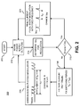
- FIG. 2 is an example flow diagram that describes generally a method to control a power supply according to the teachings of the present invention.
- sensing of power supply output(s) occurs at block 210.
- the outputs are sensed from a winding on the input side of the power supply.
- the controller uses information sensed about the power supply output(s) to determine the peak current I PK 132 required to regulate the output with a fixed switching period T S .
- the value of peak current I PK 132 is compared to a minimum peak current I PKMIN at a decision block 220.
- the minimum peak current I PKMIN corresponds to a minimum time that output rectifier D1 114 must conduct for reliable sensing of the output voltage V o 120.
- the minimum peak current I PKMIN is 25% of the maximum peak current allowed by the design of the power supply.
- the peak current I PK 132 is determined from the magnitude of an error signal such for example U ERROR 148 in FIG. 1 .
- a small error signal typically implies a light load that demands a reduced effective switching frequency to meet the requirements of high efficiency.
- decision block 220 finds that I PK ⁇ I PKMIN , and the flow is directed to block 230.
- Peak current I PK 132 is fixed at the value I PKMIN and the period of the switching cycle T S is fixed at the value T SG in block 230. Regulation is then accomplished with minimum-sum multi-cycle modulation in a block 235.
- minimum-sum multi-cycle modulation accomplishes regulation of the output by enabling N periods of switching in the switch signal, each having period T SG , followed by no switching for M periods of T SG .
- the sum of N and M is restricted to be greater than or equal to a minimum value K, where the value of K is chosen to meet the performance requirements of the intended application.
- Minimum-sum multi-cycle modulation places a minimum value on the group period T G .
- minimum-sum multi-cycle modulation in accordance with the teachings of the present invention avoids the generation of undesirable audio frequencies while allowing the power supply to meet requirements of cost, efficiency, and output regulation.
- I PKMIN is set at approximately 25% of the peak current at maximum output power of the power supply.
- the fixed switching frequency is 30 kHz and the value of K is 6 to establish a maximum effective switching frequency of 5 kHz.
- the maximum effective switching frequency although in the range of human hearing, may be outside the range of audio frequencies that excite mechanical resonances in the components of the power supply.
- minimum-sum multi-cycle modulation may be used to regulate the delivery of low output power
- fixed frequency peak current PWM also known as fixed frequency peak current mode control
- the switch may be controlled to conduct according to a first or a second operating mode.
- a switch In the first operating mode, a switch is controlled to conduct during a fixed time within the switching period and the peak switch current within the fixed switching period is adjusted to regulate the output of a power supply.
- the switch in a second operating mode, may be controlled to conduct within a fixed switching period, one group of consecutive switching periods separated from a next group of consecutive switching periods by a time of no switching, the time of no switching is adjusted to regulate the output of the power supply.
- the time of no switching may be adjusted so that the effective switching frequency either falls outside an audible frequency range or falls below a frequency within an audible frequency range, the adjustment restricted such that the sum of the number of periods in a group where switching occurs plus the number of periods in the next group where switching does not occur is greater than or equal to a minimum value.
- period modulation also known as frequency modulation
- frequency modulation could be used instead of peak current mode PWM to regulate delivery of higher power in accordance with the teachings of the present invention.
- the decision to use period modulation versus minimum-sum multi-cycle modulation would consider the equivalent switching frequency rather than the peak current that is needed to keep the output in regulation. For example, when the switching period increases in response to the feedback signal and crosses a threshold that would indicate a light load, the operation is changed from period modulation to minimum-sum multi-cycle modulation.
- fixed frequency voltage mode PWM could be used instead of peak current mode PWM to regulate delivery of higher power in accordance with the teachings of the present invention.
- the decision to use PWM versus minimum-sum multi-cycle modulation would consider the on-time of the switch rather than peak current that is needed to keep the output in regulation. For example, when the on-time decreases in response to the feedback signal and crosses a threshold that would indicate a light load, the operation is changed from fixed frequency voltage mode PWM to minimum-sum multi-cycle modulation.
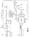
- FIG. 3 is a schematic diagram 300 that shows one example of a circuit for minimum-sum multi-cycle modulation in accordance with the teachings of the present invention.
- the schematic diagram 300 of FIG. 3 is a portion of a control circuit 140 included in an example controller 138 for an example power supply, such as for example power supply 100 of FIG. 1 .
- the minimum-sum multi-cycle modulation circuit example of FIG. 3 includes inverter 306, AND gates 308 and 334, latches 310 and 338, monostable multivibrator 312, oscillator 316 and counter 322.
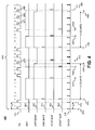
- FIG. 4 is a timing diagram 400 that shows the relationships among signals in the schematic diagram of FIG. 3 .
- oscillator 316 in FIG. 3 provides a clock signal 318 that establishes the switching frequency and marks the switching periods for the power supply.
- clock signal 318 is also distributed throughout various circuits in the controller not shown in FIG. 3 .
- FIG. 4 shows clock signal 318 marking the start of 16 consecutive switching periods 405, each with duration T S .
- the drive signal U D 154 is synchronized with the clock signal 318. The rising edge of the drive signal U D 154 in the first switching period in the sequence of switching periods 405 is coincident with the rising edge of the clock signal 318 at time to 410.
- the circuit in FIG. 3 receives a START SKIP signal 302 and a STOP SKIP signal 304 to produce a SKIP signal 342.
- the START SKIP signal 302 and the STOP SKIP signal 304 may be considered inputs, and the SKIP signal 342 may be considered the output.
- the SKIP signal 342 inhibits the drive signal U D 154 so that switching cannot occur when the SKIP signal 342 is at a high logic level.
- a simple logic circuit such as an AND gate (not shown) receiving the complement of SKIP signal 342 at one input and receiving a drive command at another input may be inhibit the drive signal U D 154 when SKIP signal 342 is high.
- a logic circuit (not shown) generates the START SKIP signal 302 and the STOP SKIP signal 304 in response to the error signal U ERROR 148.
- a logic circuit When the error signal U ERROR 148 falls below a skip threshold, a logic circuit produces a pulse that is the START SKIP signal 302.
- a logic circuit When the error signal U ERROR 148 rises above the skip threshold, a logic circuit produces a pulse that is the STOP SKIP signal 304.
- the START SKIP signal 302 would begin a sequence of switching periods where switching is prevented, and the STOP SKIP signal 304 would begin a sequence of switching periods where switching is allowed.
- the minimum-sum multi-cycle modulation circuit monitors the SKIP signal 342 and masks the START SKIP signal 302 when necessary to restrict the number of skipped periods such that the sum of the number of switching periods N in a group where switching is allowed plus the number of switching periods M in the following group where switching is prevented is greater than or equal to a minimum number K.
- switching events 470, 475, 480, and 485 of the drive signal U D 154 are marked by an asterisk to indicate that those events would have been skipped if the minimum-sum multi-cycle circuit had not masked the START SKIP signal 302 from latch 310.
- START SKIP signal 302, STOP SKIP signal 304, ONE-SHOT signal 314, SKIP MASK signal 340, and SKIP signal 342 are at a logic low level. Since SKIP signal 342 is low at time to 410, the pulse from CLOCK signal 318 at time to 410 begins an enabled switching period where the drive signal U D 154 goes high.
- Drive signal U D 154 stays high until current sense signal 136 in FIG. 1 reaches the current limit value I PK 132 also shown in FIG. 1 .
- the next switching period that begins at time t 1 415 is also an enabled switching period in which drive signal U D 154 goes high again.
- SKIP signal 342 and SKIP MASK signal 340 remain low until the START SKIP signal 302 goes high at time t 2 420.
- latch 310 sets SKIP signal 342 to a high logic level.
- a high level on SKIP signal 342 disables switching (prevents the switch S1 156 from turning on). Therefore, drive signal U D 154 stays low while SKIP signal 342 is high.
- SKIP signal 342 remains high until STOP SKIP signal 304 goes high at time t 3 425.
- monostable multivibrator 312 also called a one-shot, produces an output signal 314 that sets SKIP MASK signal 340 that is an output of latch 338 to a high logic level.
- Output signal 314 from one-shot 312 is received at a RESET input 320 of counter 322 to set outputs 326, 328, 330, and 332 to zero (low logic levels).
- Outputs 326, 328, 330, and 332 of counter 322 represent respectively the least significant to the most significant binary digits of the value of the count of counter 322.
- SKIP MASK signal 340 is also received at an ENABLE input 324 of counter 322.
- counter 322 When SKIP MASK signal 340 goes high, counter 322 begins to count pulses of the CLOCK signal 318.
- ENABLE input 324 of counter 322 may be fixed at a high logic level instead of receiving SKIP MASK signal 340 so that counter 322 counts continuously.
- a counter enabled by SKIP MASK signal 340 has reduced switching loss, whereas a counter operating continuously may provide a continuous clock signal at a reduced frequency for use by other circuits not shown in FIG. 3 .
- SKIP MASK signal 340 stays high until one or more outputs of counter 322 reaches a value that causes the output of AND gate 334 to reset latch 338.
- the value of the output of counter 322 that resets latch 338 is 6, or a binary value of 0110, because the two inputs of AND gate 334 receive outputs 328 and 330 from counter 322. Outputs 328 and 330 from counter 322 are both high when the counter reaches a value of 6.
- outputs from counter 322 may be received by an AND gate with two more inputs to reset latch 338 at a different value from counter 322.
- a more elaborate logic circuit may receive outputs from counter 322 and be logically combined with either control signals or programming signals so that the count that resets latch 322 may be changed dynamically according to the needs of the power supply.
- START SKIP signal 302 goes high at time t 4 430, but SKIP signal 342 does not go high at time t 4 430 because it is masked by SKIP MASK signal 340.
- a high logic level on SKIP MASK signal 340 is inverted by inverter 306 to apply a low logic level at an input of AND gate 308, thereby preventing START SKIP signal 302 from setting latch 310.
- FIG. 4 shows that the START SKIP signal 302 goes high at time t 4 430, but SKIP signal 342 does not go high at time t 4 430 because SKIP MASK signal 340 is high at time t 4 430, causing AND gate 308 to prevent START SKIP signal 302 from setting latch 310.
- FIG. 4 shows that START SKIP signal 302 goes high again at time t 7 445 when SKIP MASK signal 340 is low. Therefore, START SKIP signal 302 sets latch 310 to raise SKIP signal 342 to a high logic level. The transition of SKIP signal 342 produces a pulse of ONE-SHOT signal 314 from monostable multivibrator 312 that sets latch 338 and resets counter 322.
- FIG. 4 shows that SKIP signal 342 goes low at time t 8 450 in response to STOP SKIP signal 304, but SKIP signal 342 does not go high at time t 9 455 in response to START SKIP signal 302 because SKIP MASK signal 340 is still high at time t 9 455. SKIP MASK signal 340 remains high until time t 10 460, when counter 322 reaches the sixth count of CLOCK signal 318 after counter 322 was reset and enabled at time t 7 445.
- Counter 322 and AND gate 334 may be considered a filter circuit that resets SKIP MASK signal 340 in response to SKIP signal 342 and CLOCK signal 318.
- SKIP MASK signal 340 allows switching events 475, 498, and 485 to occur after START SKIP signal 302 goes high at time t 9 455.
- STOP SKIP signal 304 goes high at time t 11 465, but it has no effect because SKIP signal 342 did not go high when START SKIP signal 302 went high at time t 9 455.
- SKIP signal 342 would go high at time t 9 455 as indicated by the broken lines on SKIP signal 342 between times t 9 455 and t 11 465.
- minimum-sum multi-cycle modulation puts a lower bound on the number of enabled and disabled switching periods.
- Minimum-sum multi-cycle modulation does not impose an upper bound on either the number of enabled switching periods or the number of disabled switching periods. Therefore, under conditions of no load, switching could be disabled indefinitely by an unlimited number of skipped periods.
- controllers for power supplies that use primary side control typically have a timer that puts an upper bound on the time between switching events. In one example, a timer (not shown in controller 138) forces switch S1 156 to close at least every 4 milliseconds.
- FIG. 5 is another example flow diagram that describes generally another method to control a power supply according to the teachings of the present invention. Starting in block 505, sensing of power supply output(s) occurs at block 510.
- the controller uses information sensed about the power supply output(s) to determine an equivalent switching frequency f EQ required to regulate the power supply output with period modulation that varies the switching period T S .
- the value of the equivalent switching frequency f EQ is compared to a reference value f REF at a decision block 520.
- the reference frequency f REF is greater than or equal to the highest audio frequency of interest. In one embodiment, the reference frequency is approximately 30 kHz.
- switching frequency f EQ is estimated to be higher or lower than reference frequency f EQ on the basis of a feedback signal.
- An estimate of f EQ lower than f REF implies a light load that demands a switching frequency within the range of audio frequencies.
- decision block 520 finds that f REF > f EQ and the flow is directed to block 530. Regulation is then accomplished with minimum-sum multi-cycle regulation in block 535.
- minimum-sum multi-cycle modulation accomplishes regulation of the output by enabling N periods of switching in the switch signal, each having period T SG , followed by no switching for M periods of T SG .
- the sum of N and M is restricted to be greater than or equal to a minimum value K, where the value of K is chosen to meet the performance requirements of the intended application.
- minimum-sum multi-cycle modulation in accordance with the teachings of the present invention avoids the generation of undesirable audio frequencies while allowing the power supply to meet requirements of cost, efficiency, and output regulation.
- minimum-sum multi-cycle modulation may be used to regulate the delivery of low output power
- period modulation also known as frequency modulation
- FIG. 6 is yet another example flow diagram that describes generally yet another method to control a power supply according to the teachings of the present invention. Starting in block 605, sensing of power supply output(s) occurs at block 610.
- the controller uses information sensed about the power supply output(s) to determine an on-time T ON of a switch within a fixed switching period T S required to regulate the power supply output with pulse width modulation at a fixed switching frequency.
- the value of the on-time T ON is compared to a reference minimum value T ONMIN at a decision block 620.
- the minimum on-time is the smallest on-time that can be controlled by the control circuit.
- minimum on-time T ONMIN is approximately 600 nanoseconds. Under conditions where the control circuit cannot reduce the on-time further, a different parameter must be varied to regulate the output.
- on-time T ON is estimated to be higher or lower than the minimum value T ONMIN on the basis of a feedback signal.
- An estimate of T ON lower than T ONMIN implies a light load that demands a switching frequency within the range of audio frequencies.
- decision block 620 finds that T ONMIN > T ON and the flow is directed to block 630. Regulation is then accomplished with minimum-sum multi-cycle regulation in block 635.
- minimum-sum multi-cycle modulation accomplishes regulation of the output by enabling N periods of switching in the switch signal, each having period T SG , followed by no switching for M periods of T SG .
- the sum of N and M is restricted to be greater than or equal to a minimum value K, where the value of K is chosen to meet the performance requirements of the intended application.
- minimum-sum multi-cycle modulation in accordance with the teachings of the present invention avoids the generation of undesirable audio frequencies while allowing the power supply to meet requirements of cost, efficiency, and output regulation.
- the flow is directed to a block 625 so that regulation is accomplished with fixed frequency pulse width modulation.
- minimum-sum multi-cycle modulation may be used to regulate the delivery of low output power
- fixed frequency pulse width modulation may be used to regulate the delivery of higher output power in accordance with the teachings of the present invention.
Landscapes
- Engineering & Computer Science (AREA)
- Power Engineering (AREA)
- Dc-Dc Converters (AREA)
Description
- This invention is related to power supplies. In particular, the invention is related to controllers for switching power supplies.
- In a typical application, an ac-dc power supply receives an input that is between 100 and 240 volts rms at a relatively low frequency that is nominally either 50 Hz or 60 Hz from an ordinary ac electrical outlet. The ac input voltage is usually rectified within the power supply to become a source of unregulated dc voltage for use by a dc-dc switching power converter. Switches in the power converter are typically switched on and off at a relatively high frequency (tens or hundreds of kilohertz) by a control circuit to provide a regulated output that may be suitable for operating an electronic device, or for charging a battery that provides power to an electronic device.
- The design of a switching power supply is usually a compromise among conflicting requirements of efficiency, size, weight, and cost. The optimal solution that delivers the rated output power usually sets the switching frequency much higher than 20 kHz, outside the range of human hearing.
- Regulatory requirements limit the amount of energy power supplies can consume when they operate at low loads, such as standby loads and at no load. When a switching power supply delivers much less than its rated power, the energy lost within the power supply is dominated by losses from the action of switching. Therefore, it is beneficial for the power supply to operate at lower switching frequencies when the output power is low to reduce the dominant losses.
- The optimal switching frequency at low power often falls within the band of audio frequencies below 20 kHz. Switching within the band of audio frequencies can produce undesirable audio noise that results from mechanical excitation of electrical and magnetic components in the power supply. It is difficult to adjust the frequency of an oscillator in a continuous way to avoid the undesirable audio frequencies while meeting requirements for the power supply to be stable and to respond adequately to changes in load.
- To overcome this difficulty, controllers for power supplies typically set an oscillator at a fixed frequency, and they regulate the output by allowing and preventing switching during the switching periods defined by the oscillator. The switching periods of the oscillator are sometimes referred to as switching cycles. The resulting groups of consecutive switching and non-switching periods produce an effective switching frequency that may be substantially less than the frequency of the oscillator. The effective switching frequency may be thought of as an average switching frequency that is substantially the fixed oscillator frequency multiplied by the ratio of the number of times switching occurs in a large number of consecutive switching periods divided by the large number of consecutive switching periods.
- The switching periods where switching occurs are sometimes called enabled switching periods and the periods where switching is prevented are sometimes called disabled switching periods or skipped switching periods. It is important to distribute the enabled periods and the skipped periods in a way that avoids the generation of audio noise while allowing the power supply to switch often enough for it to respond adequately to changes in load. The requirement for galvanic isolation can place restrictions on the grouping of enabled periods and skipped periods.
- Safety agencies generally require galvanic isolation between the input and the output of an ac to dc power supply. Galvanic isolation prevents dc current between the input and the output of the power supply. In other words, a high dc voltage applied between an input terminal and an output terminal of the power supply will produce no dc current between the input terminal and the output terminal of the power supply. The requirement for galvanic isolation is a complication that contributes to the cost of the power supply and to the difficulty of avoiding switching at undesirable audio frequencies.
- A power supply with galvanic isolation must maintain an isolation barrier that electrically separates the input from the output such that circuits on the input side of the isolation barrier are galvanically isolated from the circuits on the output side of the isolation barrier. Energy must be transferred across the isolation barrier to provide power to the output, and information in the form of signals must be transferred across the isolation barrier to regulate the output. Galvanic isolation is typically achieved with electromagnetic and electro-optical devices. Electromagnetic devices such as transformers and coupled inductors are generally used to transfer energy between input and output to provide output power, whereas electro-optical devices are generally used to transfer signals between output and input to control the transfer of energy between input and output.
- Efforts to reduce the cost of the power supply have focused on the elimination of electro-optical devices and their associated circuits. Alternative solutions generally use a single energy transfer element such as a transformer or coupled inductor to provide energy to the output and also to obtain the information necessary to control the output. The lowest cost configuration typically places the control circuit and a high voltage switch on the input side of the isolation barrier.
- The controller obtains information about the output indirectly from observation of a voltage at either a winding of the energy transfer element or a winding of another switched electromagnetic element. The winding that provides the information is on the input side of the isolation barrier. To reduce cost and complexity further, the controller can also use the same winding of the energy transfer element to obtain information about the input to the power supply. A difficulty with the use of a switched magnetic element to obtain the information necessary to control the power supply is that the controller receives no information during periods where there is no switching. Therefore, the controller must force the switch to switch often enough for it to respond adequately to changes in the load.
- The input side of the isolation barrier is sometimes referred to as the primary side, and the output side of the isolation barrier is sometimes referred to as the secondary side. Windings of the energy transfer element that are not galvanically isolated from the primary side are also primary side windings, sometimes called primary referenced windings. A winding on the primary side that is coupled to an input voltage and receives energy from the input voltage is sometimes referred to simply as the primary winding. Other primary referenced windings that deliver energy to circuits on the primary side may have names that describe their principal function, such as for example a bias winding, or for example a sense winding. Windings that are galvanically isolated from the primary side windings are secondary side windings, sometimes called output windings.
- Power supply controllers that obtain information about an output on the secondary side from a winding on the primary side, especially when the information is in the form of a pulsating signal, are sometimes referred to as having primary side controllers, and the power supplies are said to operate with primary side control.
- Existing controllers for power supplies that reduce the effective switching frequency by either allowing or preventing switching during groups of switching periods have difficulty meeting cost and performance requirements in galvanically isolated applications. A low-cost solution is needed for primary side controllers to avoid effective switching frequencies that fall within the range of undesirable audio frequencies while allowing adequate control of the output.
-
European published patent application No. 1 909 382 A2 discloses and apparatus and a method of switching a switch of a power supply are disclosed. The method includes controlling a switch of a switching power supply to switch on and off within a switching cycle. The switch cycle has a substantially fixed period. One group of consecutive switching cycles (N Periods) is separated from a next group of consecutive switching cycles (N Periods) by a time of no switching (M TSG). Each group of consecutive switching cycles (N Periods) has at least a predetermined minumum of two of more switching cycles (TSG). The time of no switching (M TSG) is adjusted in a closed loop to regulate an output of the switching power supply. -
U.S. patent No. 5,745,352 describes the reduction of switching losses in a DC-to-DC converter idling in a pulse-skipping mode by inhibiting any intervening turn-off command by a PWM control loop of the converter for as long as the current through the inductor of the converter remains below a minimum threshold value set by a dedicated comparator. The method is implemented by employing a comparator with a certain hysteresis and by logically masking the switching to a logic "0" of a high frequency clock (switching) signal of the converter for the entire period of time the current in the inductor remains below the minimum threshold. - Non-limiting and non-exhaustive embodiments of the present invention are described with reference to the following figures, wherein like reference numerals refer to like parts throughout the various views unless otherwise specified.
-
FIG. 1 is a functional block diagram that shows an example of a power supply with a primary side controller in accordance with the teachings of the present invention. -
FIG. 2 is an example flow diagram illustrating generally a sample flow of operations of an example switching power supply providing power to a load in accordance with the teachings of the present invention. -
FIG. 3 is schematic diagram showing a portion of an example controller for a power supply that illustrates an example circuit for minimum-sum multi-cycle modulation in accordance with the teachings of the present invention. -
FIG. 4 is a timing diagram that shows signals in the example minimum-sum multi-cycle modulation circuit example shown inFIG. 3 . -
FIG. 5 is another example flow diagram illustrating generally a sample flow of operations of another example switching power supply providing power to a load in accordance with the teachings of the present invention. -
FIG. 6 is yet another example flow diagram illustrating generally a sample flow of operations of another example switching power supply providing power to a load in accordance with the teachings of the present invention. - Methods and apparatuses for controlling a power supply with minimum-sum muti-cycle modulation are disclosed. In the following description, numerous specific details are set forth in order to provide a thorough understanding of the present invention. It will be apparent, however, to one having ordinary skill in the art that the specific detail need not be employed to practice the present invention. In other instances, well-known materials or methods have not been described in detail in order to avoid obscuring the present invention.
- Reference throughout this specification to "one embodiment", "an embodiment", "one example" or "an example" means that a particular feature, structure or characteristic described in connection with the embodiment or example is included in at least one embodiment of the present invention. Thus, appearances of the phrases "in one embodiment", "in an embodiment", "one example" or "an example" in various places throughout this specification are not necessarily all referring to the same embodiment or example. Furthermore, the particular features, structures or characteristics may be combined in any suitable combinations and/or subcombinations in one or more embodiments or examples. Particular features, structures or characteristics may be included in an integrated circuit, an electronic circuit, a combinational logic circuit, or other suitable components that provide the described functionality. In addition, it is appreciated that the figures provided herewith are for explanation purposes to persons ordinarily skilled in the art and that the drawings are not necessarily drawn to scale.
- To illustrate, the schematic diagram of
FIG. 1 shows salient features of one example of a dc-dc power supply 100 with galvanic isolation that receives aninput voltage V IN 102 to produce anoutput voltage V o 120 and an output current Io 118 to a load (not shown inFIG. 1 ) in accordance with the teachings of the present invention. In an example of an ac-dc power supply, the dcinput voltage V IN 102 may be a rectified and filtered ac input voltage.Input voltage V IN 102 is positive with respect to aninput return 104.Output voltage V o 120 is positive with respect to anoutput return 122. In other examples, the power supply may have more than one output. - The dc-
dc power supply 100 in the example ofFIG. 1 includes an energytransfer element T1 124 and aswitch S1 156. Theswitch S1 156 represents the operation of a controlled semiconductor device such as for example a metal oxide semiconductor field effect transistor (MOSFET) or for example a bipolar junction transistor (BJT). The dc-dc power supply 100 in the example ofFIG. 1 also includes acontroller 138 that receives acurrent sense signal 136 and avoltage sense signal 152. In the example ofFIG. 1 , avoltage sense circuit 130 produces a pulsatingvoltage V B 128 that may be positive and negative with respect to theinput return 104. - In the example illustrated in
FIG. 1 , energytransfer element T1 124 is a coupled inductor, sometimes referred to as a transformer, with three windings. Winding 110 is a primary winding that has one end coupled to theinput voltage V IN 102 and the opposite end coupled to theswitch S1 156. Winding 112 is a secondary winding that has one end coupled to theoutput return 122 and the opposite end coupled to anoutput rectifier D1 114. Winding 126 is a sense winding, sometimes referred to as a bias winding, with one end coupled to theinput return 104. The polarities of the windings, indicated by the dots at one end of each winding (dotted ends have the same polarity), show that the example ofFIG. 1 is configured to be a flyback power supply. - In the operation of the flyback power supply example of
FIG. 1 ,controller 138 produces a drive signal UD) 154 that may open and close switch S1156 within repetitive switching periods of duration TS. Whenswitch S 1 156 is closed (also referred to as being ON or being in an ON state), theswitch S1 156 may conduct current IP 134 in the primary winding 110 ofenergy transfer element 124. Whenswitch S1 156 is open (also referred to as being OFF or being in an OFF state), theswitch S1 156 cannot conduct current. - When
switch S1 156 is ON, thevoltage V P 108 across the primary winding 110 of theenergy transfer element 124 is theinput voltage V IN 102. While switch S1 is ON in the example ofFIG. 1 , primary current IP 134 increases until it reaches a value of a variablecurrent limit I PK 132. In the example ofFIG. 1 , there is substantially no current in secondary winding 112 and substantially no current in sense winding 126 whileswitch S1 156 is ON. -
Controller 138 senses a pulsating primary current IP 134 that is also the current in theswitch S1 156 as acurrent sense signal 136. Any of the many known ways to sense current, such as for example receiving the voltage across a resistor conducting the current, or for example receiving a scaled current from a current transformer, or for example receiving the voltage across the on-resistance of a metal oxide semiconductor field-effect transistor (MOSFET) that conducts the current, may be used to sense the primary current IP 134 and to providecurrent signal 136 tocontroller 138. - The waveforms of current and voltage illustrated in the example of
FIG. 1 show that thepower supply 100 is operating in the discontinuous conduction mode (DCM), which is typical for operation at light loads. A distinguishing characteristic of operation in DCM is that the primary current IP 134 is zero immediately after theswitch S1 156 turns ON. At higher loads, the power supply typically operates in the continuous conduction mode (CCM), which is distinguished by a jump in primary current IP 134 from zero to a finite positive value immediately after theswitch S1 156 turns ON, not shown inFIG. 1 . - When primary current IP 134 reaches the value of a variable current limit IPK 132,
controller 138 opensswitch S1 156 andcurrent I P 134 falls to zero. Aclamp circuit 106 is typically coupled across primary winding 110 to limit the voltage onswitch S1 156 whenswitch S1 156 opens. - When
controller 138 opens theswitch S1 156, energy stored in coupledinductor T1 124 while theswitch S1 156 was conducting produces a current in secondary winding 112. The pulsating current in secondary winding 112 is rectified bydiode D1 114 and filtered bycapacitor C1 116 to produce a substantially dcoutput voltage V o 120. - The switching of
switch S1 156 produces avoltage V B 128 on bias winding 126 that is related by transformer action to the voltages on primary winding 110 and secondary winding 112. Whenswitch S1 156 is ON, thevoltage V B 128 is negative with respect to theoutput return 104 with a magnitude that is substantially theinput voltage V IN 102 scaled by the turns ratio that is the number of turns on winding 126 divided by the number of turns on winding 110. Whenswitch S1 156 turns OFF anddiode D1 114 is conducting, thevoltage V B 128 is positive with respect to theoutput return 104 with a value that is substantially theoutput voltage V O 120 plus the voltage acrossdiode D1 114 when the diode is conducting, the sum scaled by the turns ratio, which is the number of turns on winding 126 divided by the number of turns on winding 112. -
Controller 138 in the example ofFIG. 1 includes asignal separator 150 to extract the sensed input voltage VINSENSE and the sensed output voltage VOSENSE from voltagesense signal V SENSE 152. In one example,signal separator 150 may be a rectifier followed by a sample and hold circuit that provides a substantially dcfeedback signal U FB 144 that is representative of theoutput voltage V o 120. -
Controller 138 in the example ofFIG. 1 also includes anerror amplifier 146 that produces anerror signal U ERROR 148 from the difference between thefeedback signal U FB 144 and areference signal U REF 142. Thereference signal U REF 142 is representative of the desired value of theoutput V o 120, whereas thefeedback signal U FB 144 is representative of the actual value of theoutput voltage V o 120. In one example,error amplifier 146 includes an integrator that integrates the difference between thereference signal U REF 142 and thefeedback signal U FB 144. In other examples,error amplifier 146 may include a differentiator as well as an integrator to provide desired characteristics for the stability and the behavior of the power supply in response changes ininput voltage V IN 102 and output current IO 118 as is well known in the art. -
Controller 138 in the example ofFIG. 1 also includes acontrol circuit 140 that receives theerror signal U ERROR 148 and produces thedrive signal U D 154 that switches theswitch S1 156.Control circuit 140 in the example ofFIG. 1 may include various analog and digital circuits such as for example counters 158, logic gates160, andoscillators 158, to provide the desired relationships among theerror signal U ERROR 148, thecurrent sense signal 136, and thedrive signal U D 154. - The
control circuit 140 may filter thecurrent sense signal 136 and the error signal 148 UERROR in various ways to provide the desired behavior of the power supply under a variety of conditions such as for example, startup, shutdown, overload, light load, and no-load. - In one example,
control circuit 140 adjusts the value of the variable current limit IPK 132 in response to theerror signal U ERROR 148 so that theoutput voltage V o 120 is regulated at a desired value. When the switching period TS is fixed, adjustment of the variable current limit IPK 132 changes the duration that theswitch S1 156 is ON, sometimes referred to as the on-time. The duration that theswitch S1 156 is ON is also sometimes referred to as the on-time interval of the cycle. This type of control may be described as peak current pulse width modulation (PWM) with fixed frequency. It is sometimes referred to as fixed frequency peak current mode control or just current mode control. - In other examples, the
control circuit 140 may directly adjust the time that theswitch S1 156 is ON within a fixed switching period when the primary current 134 is less than a fixed current limit. This type of control sometimes referred to as fixed frequency voltage mode PWM, or fixed frequency duty ratio control. - In yet other examples, the
control circuit 140 may fix the on-time of the switch when the primary current 134 is less than a fixed current limit and it may adjust a variable switching period to regulate the output. Alternatively, thecontrol circuit 140 may set a fixed current limit to turn the switch OFF, and it may adjust a variable switching period to regulate the output. The control circuit may vary the length of time the switch is ON and OFF in many different ways to regulate the output of the power supply at moderate to heavy loads. - At light loads the
controller 138 may use a circuit to control the power supply such that switching events are gathered into groups of consecutive periods where switching occurs, separated by groups of consecutive periods where switching does not occur, and the sum of the number of periods in a group where switching occurs plus the number of periods in a group where switching does not occur is always greater than or equal to a minimum value. This type of control may be described as minimum-sum multi-cycle modulation. In one example, the sum of the number of enabled periods plus the number of skipped periods is a constant. Minimum-sum multi-cycle modulation restricts the grouping of enabled periods and skipped periods to avoid effective switching frequencies that fall within the range of undesirable audio frequencies while allowing adequate control of the output. -
FIG. 2 is an example flow diagram that describes generally a method to control a power supply according to the teachings of the present invention. Starting inblock 205, sensing of power supply output(s) occurs atblock 210. In a power supply with primary side control, the outputs are sensed from a winding on the input side of the power supply. - Next, in
block 215, the controller uses information sensed about the power supply output(s) to determine the peak current IPK 132 required to regulate the output with a fixed switching period TS. Next, the value of peak current IPK 132 is compared to a minimum peak current IPKMIN at adecision block 220. In one example, the minimum peak current IPKMIN corresponds to a minimum time thatoutput rectifier D1 114 must conduct for reliable sensing of theoutput voltage V o 120. In one example, the minimum peak current IPKMIN is 25% of the maximum peak current allowed by the design of the power supply. - In one example, the peak current IPK 132 is determined from the magnitude of an error signal such for
example U ERROR 148 inFIG. 1 . A small error signal typically implies a light load that demands a reduced effective switching frequency to meet the requirements of high efficiency. Under those conditions,decision block 220 finds that IPK < IPKMIN, and the flow is directed to block 230. Peakcurrent I PK 132 is fixed at the value IPKMIN and the period of the switching cycle TS is fixed at the value TSG inblock 230. Regulation is then accomplished with minimum-sum multi-cycle modulation in ablock 235. - As shown in
block 235, minimum-sum multi-cycle modulation accomplishes regulation of the output by enabling N periods of switching in the switch signal, each having period TSG, followed by no switching for M periods of TSG. In the example, the sum of N and M is restricted to be greater than or equal to a minimum value K, where the value of K is chosen to meet the performance requirements of the intended application. Minimum-sum multi-cycle modulation places a minimum value on the group period TG. In the example, minimum-sum multi-cycle modulation in accordance with the teachings of the present invention avoids the generation of undesirable audio frequencies while allowing the power supply to meet requirements of cost, efficiency, and output regulation. - In one example, IPKMIN is set at approximately 25% of the peak current at maximum output power of the power supply. In one embodiment, the fixed switching frequency is 30 kHz and the value of K is 6 to establish a maximum effective switching frequency of 5 kHz. The maximum effective switching frequency, although in the range of human hearing, may be outside the range of audio frequencies that excite mechanical resonances in the components of the power supply.
- If the
decision block 220 finds that IPKMIN ≤ IPK, then the flow is directed to ablock 225 so that regulation is accomplished with peak current PWM at fixed switching frequency instead of minimum-sum multi-cycle modulation. In one example, minimum-sum multi-cycle modulation may be used to regulate the delivery of low output power, and fixed frequency peak current PWM (also known as fixed frequency peak current mode control) may be used to regulate the delivery of higher output power in accordance with the teachings of the present invention. - Thus, in one example, dependent upon the relationship between peak switch current IPK and minimum peak switch current IPKMIN, the switch may be controlled to conduct according to a first or a second operating mode. In the first operating mode, a switch is controlled to conduct during a fixed time within the switching period and the peak switch current within the fixed switching period is adjusted to regulate the output of a power supply. Alternatively, in a second operating mode, the switch may be controlled to conduct within a fixed switching period, one group of consecutive switching periods separated from a next group of consecutive switching periods by a time of no switching, the time of no switching is adjusted to regulate the output of the power supply. In the example, the time of no switching may be adjusted so that the effective switching frequency either falls outside an audible frequency range or falls below a frequency within an audible frequency range, the adjustment restricted such that the sum of the number of periods in a group where switching occurs plus the number of periods in the next group where switching does not occur is greater than or equal to a minimum value.
- In one example, period modulation, also known as frequency modulation, could be used instead of peak current mode PWM to regulate delivery of higher power in accordance with the teachings of the present invention. In that example, the decision to use period modulation versus minimum-sum multi-cycle modulation would consider the equivalent switching frequency rather than the peak current that is needed to keep the output in regulation. For example, when the switching period increases in response to the feedback signal and crosses a threshold that would indicate a light load, the operation is changed from period modulation to minimum-sum multi-cycle modulation.
- In another example, fixed frequency voltage mode PWM could be used instead of peak current mode PWM to regulate delivery of higher power in accordance with the teachings of the present invention. In that example, the decision to use PWM versus minimum-sum multi-cycle modulation would consider the on-time of the switch rather than peak current that is needed to keep the output in regulation. For example, when the on-time decreases in response to the feedback signal and crosses a threshold that would indicate a light load, the operation is changed from fixed frequency voltage mode PWM to minimum-sum multi-cycle modulation.
-
FIG. 3 is a schematic diagram 300 that shows one example of a circuit for minimum-sum multi-cycle modulation in accordance with the teachings of the present invention. The schematic diagram 300 ofFIG. 3 is a portion of acontrol circuit 140 included in anexample controller 138 for an example power supply, such as forexample power supply 100 ofFIG. 1 . As shown, the minimum-sum multi-cycle modulation circuit example ofFIG. 3 includesinverter 306, ANDgates monostable multivibrator 312,oscillator 316 andcounter 322.FIG. 4 is a timing diagram 400 that shows the relationships among signals in the schematic diagram ofFIG. 3 . - In the depicted example,
oscillator 316 inFIG. 3 provides aclock signal 318 that establishes the switching frequency and marks the switching periods for the power supply. In one example,clock signal 318 is also distributed throughout various circuits in the controller not shown inFIG. 3 .FIG. 4 showsclock signal 318 marking the start of 16consecutive switching periods 405, each with duration TS. In the example ofFIG. 4 , thedrive signal U D 154 is synchronized with theclock signal 318. The rising edge of thedrive signal U D 154 in the first switching period in the sequence of switchingperiods 405 is coincident with the rising edge of theclock signal 318 at time to 410. - When the power supply operates with minimum-sum multi-cycle modulation, the circuit in
FIG. 3 receives aSTART SKIP signal 302 and aSTOP SKIP signal 304 to produce aSKIP signal 342. In the minimum-sum multi-cycle modulation circuit ofFIG. 3 , the START SKIP signal 302 and theSTOP SKIP signal 304 may be considered inputs, and theSKIP signal 342 may be considered the output. In one example, theSKIP signal 342 inhibits thedrive signal U D 154 so that switching cannot occur when theSKIP signal 342 is at a high logic level. In one example, a simple logic circuit such as an AND gate (not shown) receiving the complement ofSKIP signal 342 at one input and receiving a drive command at another input may be inhibit thedrive signal U D 154 whenSKIP signal 342 is high. - In one example, a logic circuit (not shown) generates the
START SKIP signal 302 and theSTOP SKIP signal 304 in response to theerror signal U ERROR 148. When theerror signal U ERROR 148 falls below a skip threshold, a logic circuit produces a pulse that is theSTART SKIP signal 302. When theerror signal U ERROR 148 rises above the skip threshold, a logic circuit produces a pulse that is theSTOP SKIP signal 304. - In the absence of the minimum-sum multi-cycle modulation circuit explained below, the START SKIP signal 302 would begin a sequence of switching periods where switching is prevented, and the
STOP SKIP signal 304 would begin a sequence of switching periods where switching is allowed. In the example ofFIG. 3 , the minimum-sum multi-cycle modulation circuit monitors theSKIP signal 342 and masks the START SKIP signal 302 when necessary to restrict the number of skipped periods such that the sum of the number of switching periods N in a group where switching is allowed plus the number of switching periods M in the following group where switching is prevented is greater than or equal to a minimum number K. - In the timing diagram of
FIG. 4 , switchingevents drive signal U D 154 are marked by an asterisk to indicate that those events would have been skipped if the minimum-sum multi-cycle circuit had not masked the START SKIP signal 302 fromlatch 310. At time to 410,START SKIP signal 302,STOP SKIP signal 304, ONE-SHOT signal 314,SKIP MASK signal 340, andSKIP signal 342 are at a logic low level. SinceSKIP signal 342 is low at time to 410, the pulse fromCLOCK signal 318 at time to 410 begins an enabled switching period where thedrive signal U D 154 goes high.Drive signal U D 154 stays high untilcurrent sense signal 136 inFIG. 1 reaches the current limit value IPK 132 also shown inFIG. 1 . The next switching period that begins attime t 1 415 is also an enabled switching period in which drivesignal U D 154 goes high again. -
SKIP signal 342 and SKIP MASK signal 340 remain low until the START SKIP signal 302 goes high attime t 2 420. When START SKIP signal 302 goes high attime t 2 420, latch 310sets SKIP signal 342 to a high logic level. A high level onSKIP signal 342 disables switching (prevents theswitch S1 156 from turning on). Therefore,drive signal U D 154 stays low whileSKIP signal 342 is high.SKIP signal 342 remains high untilSTOP SKIP signal 304 goes high attime t 3 425. - When SKIP signal 342 goes to a high logic level at
time t 2 420,monostable multivibrator 312, also called a one-shot, produces anoutput signal 314 that setsSKIP MASK signal 340 that is an output oflatch 338 to a high logic level.Output signal 314 from one-shot 312 is received at aRESET input 320 ofcounter 322 to setoutputs Outputs counter 322 represent respectively the least significant to the most significant binary digits of the value of the count ofcounter 322.SKIP MASK signal 340 is also received at anENABLE input 324 ofcounter 322. When SKIP MASK signal 340 goes high,counter 322 begins to count pulses of theCLOCK signal 318. In other examples, ENABLEinput 324 ofcounter 322 may be fixed at a high logic level instead of receivingSKIP MASK signal 340 so that counter 322 counts continuously. A counter enabled by SKIP MASK signal 340 has reduced switching loss, whereas a counter operating continuously may provide a continuous clock signal at a reduced frequency for use by other circuits not shown inFIG. 3 . - SKIP MASK signal 340 stays high until one or more outputs of
counter 322 reaches a value that causes the output of ANDgate 334 to resetlatch 338. In the example ofFIG. 3 , the value of the output ofcounter 322 that resetslatch 338 is 6, or a binary value of 0110, because the two inputs of ANDgate 334 receiveoutputs counter 322.Outputs counter 322 are both high when the counter reaches a value of 6. - In another example, other outputs from
counter 322 may be received by an AND gate with two more inputs to resetlatch 338 at a different value fromcounter 322. In yet another example, a more elaborate logic circuit may receive outputs fromcounter 322 and be logically combined with either control signals or programming signals so that the count that resetslatch 322 may be changed dynamically according to the needs of the power supply. - In the example timing diagram of
FIG. 4 , START SKIP signal 302 goes high attime t 4 430, butSKIP signal 342 does not go high attime t 4 430 because it is masked bySKIP MASK signal 340. A high logic level onSKIP MASK signal 340 is inverted byinverter 306 to apply a low logic level at an input of ANDgate 308, thereby preventing START SKIP signal 302 from settinglatch 310. In the absence of the minimum-sum multi-cycle modulation circuit ofFIG. 3 ,SKIP signal 342 inFIG. 4 would go high attime t 4 430 and would go low attime t 6 440 in response to START SKIP signal 302 and STOP SKIP signal 304 respectively, as indicated by the dashed lines onSKIP signal 342 inFIG. 4 betweentimes t 4 430 andt 6 440. - In the example of
FIG. 4 ,SKIP MASK signal 340 goes high attime t 2 420 and stays high for K counts ofCLOCK signal 318, going low attime t 5 435. SinceFIG. 4 shows the operation of the example circuit ofFIG. 3 , K = 6 and theSKIP MASK signal 340 goes low on the sixth pulse ofCLOCK signal 318 afterSKIP MASK signal 340 enables counter 322 attime t 2 420. -
FIG. 4 shows that the START SKIP signal 302 goes high attime t 4 430, butSKIP signal 342 does not go high attime t 4 430 becauseSKIP MASK signal 340 is high attime t 4 430, causing ANDgate 308 to prevent START SKIP signal 302 from settinglatch 310. - The example of
FIG. 4 shows that START SKIP signal 302 goes high again attime t 7 445 when SKIP MASK signal 340 is low. Therefore, START SKIP signal 302 sets latch 310 to raise SKIP signal 342 to a high logic level. The transition ofSKIP signal 342 produces a pulse of ONE-SHOT signal 314 frommonostable multivibrator 312 that setslatch 338 and resets counter 322. - The example of
FIG. 4 shows thatSKIP signal 342 goes low attime t 8 450 in response to STOPSKIP signal 304, butSKIP signal 342 does not go high attime t 9 455 in response to START SKIP signal 302 becauseSKIP MASK signal 340 is still high attime t 9 455. SKIP MASK signal 340 remains high untiltime t 10 460, whencounter 322 reaches the sixth count ofCLOCK signal 318 aftercounter 322 was reset and enabled attime t 7 445.Counter 322 and ANDgate 334 may be considered a filter circuit that resetsSKIP MASK signal 340 in response to SKIP signal 342 andCLOCK signal 318. - In the example of
FIG. 4 ,SKIP MASK signal 340 allows switchingevents time t 9 455.STOP SKIP signal 304 goes high attime t 11 465, but it has no effect becauseSKIP signal 342 did not go high when START SKIP signal 302 went high attime t 9 455. In the absence of the minimum-sum multi-cycle modulation circuit,SKIP signal 342 would go high attime t 9 455 as indicated by the broken lines onSKIP signal 342 betweentimes t 9 455 andt 11 465. - As illustrated by the examples of
FIG. 3 andFIG. 4 , minimum-sum multi-cycle modulation puts a lower bound on the number of enabled and disabled switching periods. Minimum-sum multi-cycle modulation does not impose an upper bound on either the number of enabled switching periods or the number of disabled switching periods. Therefore, under conditions of no load, switching could be disabled indefinitely by an unlimited number of skipped periods. To avoid problems with extended times of no switching, controllers for power supplies that use primary side control typically have a timer that puts an upper bound on the time between switching events. In one example, a timer (not shown in controller 138) forces switchS1 156 to close at least every 4 milliseconds. -
FIG. 5 is another example flow diagram that describes generally another method to control a power supply according to the teachings of the present invention. Starting inblock 505, sensing of power supply output(s) occurs atblock 510. - Next, in
block 515, the controller uses information sensed about the power supply output(s) to determine an equivalent switching frequency fEQ required to regulate the power supply output with period modulation that varies the switching period TS. Next, the value of the equivalent switching frequency fEQ is compared to a reference value fREF at adecision block 520. In one example, the reference frequency fREF is greater than or equal to the highest audio frequency of interest. In one embodiment, the reference frequency is approximately 30 kHz. - In one example, switching frequency fEQ is estimated to be higher or lower than reference frequency fEQ on the basis of a feedback signal. An estimate of fEQ lower than fREF implies a light load that demands a switching frequency within the range of audio frequencies. Under these conditions,
decision block 520 finds that fREF > fEQ and the flow is directed to block 530. Regulation is then accomplished with minimum-sum multi-cycle regulation inblock 535. - As shown in
block 535, minimum-sum multi-cycle modulation accomplishes regulation of the output by enabling N periods of switching in the switch signal, each having period TSG, followed by no switching for M periods of TSG. In the example, the sum of N and M is restricted to be greater than or equal to a minimum value K, where the value of K is chosen to meet the performance requirements of the intended application. In the example, minimum-sum multi-cycle modulation in accordance with the teachings of the present invention avoids the generation of undesirable audio frequencies while allowing the power supply to meet requirements of cost, efficiency, and output regulation. - If the
decision block 520 finds that fREF ≤ fEQ, then the flow is directed to ablock 525 so that regulation is accomplished with period modulation instead of minimum-sum multi-cycle modulation. In one example, minimum-sum multi-cycle modulation may be used to regulate the delivery of low output power, and period modulation (also known as frequency modulation) may be used to regulate the delivery of higher output power in accordance with the teachings of the present invention. -
FIG. 6 is yet another example flow diagram that describes generally yet another method to control a power supply according to the teachings of the present invention. Starting inblock 605, sensing of power supply output(s) occurs atblock 610. - Next, in
block 615, the controller uses information sensed about the power supply output(s) to determine an on-time TON of a switch within a fixed switching period TS required to regulate the power supply output with pulse width modulation at a fixed switching frequency. Next, the value of the on-time TON is compared to a reference minimum value TONMIN at adecision block 620. In one example, the minimum on-time is the smallest on-time that can be controlled by the control circuit. In one embodiment, minimum on-time TONMIN is approximately 600 nanoseconds. Under conditions where the control circuit cannot reduce the on-time further, a different parameter must be varied to regulate the output. - In one example, on-time TON is estimated to be higher or lower than the minimum value TONMIN on the basis of a feedback signal. An estimate of TON lower than TONMIN implies a light load that demands a switching frequency within the range of audio frequencies. Under these conditions,
decision block 620 finds that TONMIN > TON and the flow is directed to block 630. Regulation is then accomplished with minimum-sum multi-cycle regulation inblock 635. - As shown in
block 635, minimum-sum multi-cycle modulation accomplishes regulation of the output by enabling N periods of switching in the switch signal, each having period TSG, followed by no switching for M periods of TSG. In the example, the sum of N and M is restricted to be greater than or equal to a minimum value K, where the value of K is chosen to meet the performance requirements of the intended application. In the example, minimum-sum multi-cycle modulation in accordance with the teachings of the present invention avoids the generation of undesirable audio frequencies while allowing the power supply to meet requirements of cost, efficiency, and output regulation. - If the
decision block 620 finds that TONMIN ≤ TON, then the flow is directed to ablock 625 so that regulation is accomplished with fixed frequency pulse width modulation. In one example, minimum-sum multi-cycle modulation may be used to regulate the delivery of low output power, and fixed frequency pulse width modulation may be used to regulate the delivery of higher output power in accordance with the teachings of the present invention. - The above description of illustrated examples of the present invention, including what is described in the Abstract, are not intended to be exhaustive or to be limitation to the precise forms disclosed. While specific embodiments of, and examples for, the invention are described herein for illustrative purposes, various equivalent modifications are possible without departing from the broader spirit and scope of the present invention. Indeed, it is appreciated that the specific example voltages, currents, frequencies, power range values, times, etc., are provided for explanation purposes and that other values may also be employed in other embodiments and examples in accordance with the teachings of the present invention.
- These modifications can be made to examples of the invention in light of the above detailed description. The terms used in the following claims should not be construed to limit the invention to the specific embodiments disclosed in the specification and the claims. Rather, the scope is to be determined entirely by the following claims, which are to be construed in accordance with established doctrines of claim interpretation. The present specification and figures are accordingly to be regarded as illustrative rather than restrictive.
Claims (12)
- A power supply controller (138), comprising:a signal separator circuit (150) coupled to generate a feedback signal (144) in response to a sense signal representative of an output of a power supply (152);an error signal generator (146) coupled to generate an error signal (148) in response to the feedback signal (144) and a reference signal (142);anda control circuit (140) coupled to generate a drive signal (154) in response to the error signal (148) and a current sense signal (136), wherein the drive signal (154) is coupled to control switching of a switch (156) of the power supply, wherein the current sense signal (136) is representative of a current through the switch (156);an oscillator (162; 316) included in the control circuit (140) configured to provide a clock signal that establishes a switching frequency and marks switching periods for the power supply;characterized bya minimum-sum multi-cycle modulation circuit (300) included in the control circuit (140) and coupled to generate a skip signal (342) in response to a start skip signal (302), a stop skip signal (304) and a skip mask signal (340), wherein the skip mask signal (340) is generated in response to the skip signal (342), wherein the start skip signal (302) is coupled to cause the drive signal (154) to start skipping on-time intervals of cycles, wherein the stop skip signal (304) is coupled to cause the drive signal (156) to stop skipping the on-time intervals of cycles, and wherein the skip mask signal (340) is coupled to mask a start skip (302) signal for K consecutive clock cycles of the oscillator (162; 316) to restrict a number of skipped periods such that a sum of the number of skipped switching periods M in a group where switching is prevented plus the number of switching periods N in the following group where switching is allowed is equal to or greater than K.
- A power supply controller (138), comprising:a signal separator (150) circuit coupled to generate a feedback signal (144) in response to a sense signal representative of an output of a power supply (152);an error signal generator (146) coupled to generate an error signal (148) in response to the feedback signal (144) and a reference signal (142);anda control circuit (140) coupled to generate a drive signal (154) in response to the error signal (148) to control switching of a switch (156) of the power supply to regulate the output of the power supply, wherein the control circuit (140) further comprises:a frequency variation circuit coupled to vary a switching frequency of the drive signal (154) in response to the error signal (148) to regulate the output of the power supply or a pulse width modulation circuit coupled to vary a pulse width of an on-time interval of each cycle of the drive signal (154) in response to the error signal (148) to regulate the output of the power supply; andan oscillator (162; 316) included in the control circuit (140) configured to provide a clock signal that establishes a switching frequency and marks switching periods for the power supply;characterized bya minimum-sum multi-cycle modulation (300) circuit coupled to generate a skip signal (342) in response to a start skip signal (302), a stop skip signal (304) and a skip mask signal (340) when the switching frequency of the drive signal (154) is greater than a threshold switching frequency value if the control circuit (140) comprises a frequency variation circuit or when the on-time interval of cycles of the drive signal (154) is less than a threshold on-time value if the control circuit (140) comprises a pulse width modulation circuit, wherein the skip mask signal (340) is generated in response to the skip signal (342), wherein the start skip signal (302) is coupled to cause the drive signal (154) to start skipping on-time intervals of cycles, wherein the stop skip signal (304) is coupled to cause the drive signal (154) to stop skipping the on-time intervals of cycles, and wherein the skip mask signal (340) is coupled to mask a start skip (302) signal for K consecutive clock cycles of the oscillator (162; 316) to restrict a number of skipped periods such that a sum of the number of skipped switching periods M in a group where switching is prevented plus the number of switching periods N in the following group where switching is allowed is equal to or greater than K.
- The power supply controller of claims 1 or 2, wherein the multi-cycle modulation circuit (300) is configured to put a lower bound on a number of skipped and non-skipped cycles.
- The power supply controller of anyone of claims I to 3 wherein the multi-cycle modulation circuit (300) further comprises a filter circuit (322, 334) coupled to reset the skip mask signal (340) in response to skip signal (342) and a clock signal (318).
- The power supply controller of claim 4 wherein the multi-cycle modulation circuit (300) further comprises a first latch (338) coupled to generate the skip mask signal (340), wherein the first latch (338) is coupled to be set in response to the skip signal (342) and wherein the first latch (338) is coupled to be reset in response to the filter circuit (322, 334).
- The power supply controller of claim 5 wherein the multi-cycle modulation circuit (300) further comprises a one-shot circuit (312) coupled to set the first latch (338) in response to the skip signal (342).
- The power supply controller of claim 4 wherein the multi-cycle modulation circuit (300) further comprises the oscillator (316) coupled to generate the clock signal (318).
- The power supply controller of claim 4 wherein the filter circuit (322, 334) comprises a counter (322) coupled to be clocked in response to the clock signal (318), wherein the counter (322) is further coupled to be reset in response to the skip signal (342).
- The power supply controller of claim 8 wherein the filter circuit (322, 334) further comprises a first logical AND gate (334) coupled to reset the skip mask signal (340) in response to one or more outputs of the counter (322).
- The power supply controller of anyone of claims 1 to 3 wherein the multi-cycle modulation circuit (300) further comprises a second latch (310) coupled to generate the skip signal (342), wherein the second latch (310) is coupled to be set in response to the start skip signal (302) and the skip mask signal (340) and wherein the second latch (310) is coupled to be reset in respond to the stop skip signal (304).
- The power supply controller of anyone of claims 1 to 3 wherein the start skip signal (302) and the stop skip signal (304) are generated in response to the error signal (148).
- The power supply controller of claim 1 wherein the control circuit (140) further comprises a current limit circuit coupled to generate a variable current limit signal to regulate the output of the power supply, the current limit circuit coupled to terminate an on-time interval of each cycle of the drive signal (154) in response to current sense signal (136) and a variable current limit signal, wherein the multi-cycle modulation circuit (300) is coupled to generate the skip signal (342) in response to the start skip signal (302), the stop skip signal (304) and the skip mask signal (340) when the variable current limit signal is less than a threshold current limit value.
Applications Claiming Priority (1)
| Application Number | Priority Date | Filing Date | Title |
|---|---|---|---|
| US13/242,947 US8693217B2 (en) | 2011-09-23 | 2011-09-23 | Power supply controller with minimum-sum multi-cycle modulation |
Publications (3)
| Publication Number | Publication Date |
|---|---|
| EP2573922A2 EP2573922A2 (en) | 2013-03-27 |
| EP2573922A3 EP2573922A3 (en) | 2014-04-09 |
| EP2573922B1 true EP2573922B1 (en) | 2016-07-27 |
Family
ID=47040539
Family Applications (1)
| Application Number | Title | Priority Date | Filing Date |
|---|---|---|---|
| EP12185147.1A Not-in-force EP2573922B1 (en) | 2011-09-23 | 2012-09-20 | Power supply controller with minimum-sum multi-cycle modulation |
Country Status (4)
| Country | Link |
|---|---|
| US (2) | US8693217B2 (en) |
| EP (1) | EP2573922B1 (en) |
| JP (1) | JP6170659B2 (en) |
| CN (1) | CN103023333B (en) |
Families Citing this family (26)
| Publication number | Priority date | Publication date | Assignee | Title |
|---|---|---|---|---|
| US7471530B2 (en) | 2006-10-04 | 2008-12-30 | Power Integrations, Inc. | Method and apparatus to reduce audio frequencies in a switching power supply |
| CN102916586B (en) | 2011-08-04 | 2014-04-02 | 昂宝电子(上海)有限公司 | System and method for switching on and off power converter |
| US8693217B2 (en) | 2011-09-23 | 2014-04-08 | Power Integrations, Inc. | Power supply controller with minimum-sum multi-cycle modulation |
| US9368269B2 (en) * | 2012-10-24 | 2016-06-14 | Schumacher Electric Corporation | Hybrid battery charger |
| CN103414350B (en) * | 2013-08-29 | 2016-08-17 | 昂宝电子(上海)有限公司 | Based on loading condition regulating frequency and the system and method for electric current |
| EP3075069A1 (en) * | 2013-11-26 | 2016-10-05 | Telefonaktiebolaget LM Ericsson (publ) | A control circuit and a method for an energy based pulse skipping mode in a dc/dc converter |
| US9531284B2 (en) * | 2014-01-30 | 2016-12-27 | Silicon Laboratories Inc. | Pseudo-constant frequency control for voltage converter |
| US9531253B2 (en) | 2014-01-30 | 2016-12-27 | Silicon Laboratories Inc. | Soft-start for isolated power converter |
| US9520769B2 (en) | 2014-04-30 | 2016-12-13 | Stmicroelectronics S.R.L. | Wake up management circuit for a switching converter and related wake up method |
| US9742288B2 (en) | 2014-10-21 | 2017-08-22 | Power Integrations, Inc. | Output-side controller with switching request at relaxation ring extremum |
| US9621019B2 (en) * | 2014-11-07 | 2017-04-11 | Power Intergrations, Inc. | Indirect regulation of output current in power converter |
| US9513319B1 (en) * | 2014-11-25 | 2016-12-06 | Cypress Semiconductor Corporation | Systems, methods, and devices for energy and power metering |
| US9705412B2 (en) * | 2015-02-26 | 2017-07-11 | Stmicroelectronics S.R.L. | Pulsed feedback switching converter |
| US9577527B2 (en) * | 2015-03-20 | 2017-02-21 | Active-Semi, Inc. | Current metering for transitioning between operating modes in switching regulators |
| JP6726737B2 (en) * | 2015-09-03 | 2020-07-22 | エアロジェット ロケットダイン インコーポレイテッド | Short circuit protection for switching power converters |
| US10003269B2 (en) | 2016-01-26 | 2018-06-19 | Dialog Semiconductor Inc. | Smart Grouping control method for power converter switching noise management |
| US9893630B2 (en) * | 2016-02-26 | 2018-02-13 | Power Integrations, Inc. | Reduction of audible noise in a power converter |
| US10535394B2 (en) * | 2017-07-20 | 2020-01-14 | Samsung Electronics Co., Ltd. | Memory device including dynamic voltage and frequency scaling switch and method of operating the same |
| US11398767B2 (en) | 2017-12-06 | 2022-07-26 | Nxp B.V. | Power converter for delaying entering burst mode and method thereof |
| US10122272B1 (en) * | 2017-12-30 | 2018-11-06 | Active-Semi, Inc. | Cycle skipping prevent circuit in a regulator of a DC-to-DC converter |
| JP7066538B2 (en) * | 2018-06-07 | 2022-05-13 | キヤノン株式会社 | Power supply and image forming equipment |
| EP3959807B1 (en) | 2019-04-24 | 2023-06-07 | Power Integrations, Inc. | Power converter comprising an active non-dissipative clamp circuit, and respective controller. |
| US11632054B2 (en) | 2019-04-24 | 2023-04-18 | Power Integrations, Inc. | Mode operation detection for control of a power converter with an active clamp switch |
| US11283343B2 (en) | 2019-12-12 | 2022-03-22 | Power Integrations, Inc. | Extremum locator with measurement enable circuit |
| US11356010B2 (en) | 2020-05-11 | 2022-06-07 | Power Integrations, Inc. | Controller with frequency request circuit |
| RU2762043C1 (en) * | 2021-03-31 | 2021-12-15 | Юрий Николаевич Шуваев | Multi-tact voltage converter |
Family Cites Families (28)
| Publication number | Priority date | Publication date | Assignee | Title |
|---|---|---|---|---|
| FR2577360B1 (en) | 1985-02-08 | 1987-03-06 | Thomson Csf | AUTOMATIC STARTING CUT-OFF POWER CONTROL CIRCUIT |
| US4941078A (en) | 1989-03-07 | 1990-07-10 | Rca Licensing Corporation | Synchronized switch-mode power supply |
| US5745352A (en) * | 1994-10-27 | 1998-04-28 | Sgs-Thomson Microelectronics S.R.L. | DC-to-DC converter functioning in a pulse-skipping mode with low power consumption and PWM inhibit |
| US5751565A (en) | 1996-09-04 | 1998-05-12 | Compaq Computer Corporation | Controlling pulse skip modulation in power conversion |
| US5914865A (en) * | 1997-10-23 | 1999-06-22 | Hewlett-Packard Company | Simplified AC-DC switching converter with output isolation |
| US6456511B1 (en) | 2000-02-17 | 2002-09-24 | Tyco Electronics Corporation | Start-up circuit for flyback converter having secondary pulse width modulation |
| US6525514B1 (en) | 2000-08-08 | 2003-02-25 | Power Integrations, Inc. | Method and apparatus for reducing audio noise in a switching regulator |
| JP2002218749A (en) * | 2001-01-19 | 2002-08-02 | Sony Corp | Switching power supply unit |
| JP2003299356A (en) | 2002-04-01 | 2003-10-17 | Nanao Corp | Dc-dc converter control method |
| JP4096201B2 (en) | 2002-09-04 | 2008-06-04 | サンケン電気株式会社 | DC-DC converter |
| KR100750906B1 (en) | 2002-10-21 | 2007-08-22 | 페어차일드코리아반도체 주식회사 | Switching Mode Power Supply For Low Power Operating |
| JP2004153983A (en) | 2002-11-01 | 2004-05-27 | Sharp Corp | Switching power supply |
| KR100986762B1 (en) | 2003-09-08 | 2010-10-08 | 페어차일드코리아반도체 주식회사 | Switching power supply apparatus and power supply method thereof |
| US6998828B2 (en) | 2004-03-29 | 2006-02-14 | Semiconductor Components Industries, L.L.C. | Low audible noise power supply controller and method therefor |
| JP4033850B2 (en) * | 2004-03-31 | 2008-01-16 | 松下電器産業株式会社 | Switching power supply control semiconductor device |
| KR101020243B1 (en) | 2004-06-16 | 2011-03-07 | 페어차일드코리아반도체 주식회사 | Switching mode power supply |
| JP2005354801A (en) | 2004-07-02 | 2005-12-22 | Giga-Byte Technology Co Ltd | Replaceable power supply system for electric circuit work frequency automatic regulation, and electric circuit work frequency automatic regulating method |
| US20060049811A1 (en) | 2004-08-27 | 2006-03-09 | Thomas Farkas | Output voltage ripple reduction technique for burst mode operation of power converter |
| US7084799B1 (en) | 2005-05-09 | 2006-08-01 | Sls International, Inc. | Sigma-delta modulated amplifier |
| US7593245B2 (en) * | 2005-07-08 | 2009-09-22 | Power Integrations, Inc. | Method and apparatus to limit maximum switch current in a switching power supply |
| CN1937383A (en) * | 2005-09-22 | 2007-03-28 | 松下电器产业株式会社 | Switch power supply, semiconductor appatatus and controlling method |
| US7471530B2 (en) | 2006-10-04 | 2008-12-30 | Power Integrations, Inc. | Method and apparatus to reduce audio frequencies in a switching power supply |
| KR101274214B1 (en) * | 2006-11-30 | 2013-06-14 | 페어차일드코리아반도체 주식회사 | Switch mode power supply and the driving method thereof |
| TWI390378B (en) * | 2008-05-14 | 2013-03-21 | Richtek Technology Corp | Control circuit and method of Chi - back power converter |
| US8159843B2 (en) * | 2009-01-30 | 2012-04-17 | Power Integrations, Inc. | Method and apparatus to regulate an output voltage of a power converter at light/no load conditions |
| JP2011004550A (en) * | 2009-06-19 | 2011-01-06 | Panasonic Corp | Switching power supply apparatus and semiconductor device |
| US8379420B2 (en) * | 2010-10-13 | 2013-02-19 | Power Integrations, Inc. | Controller with punctuated switching control circuit |
| US8693217B2 (en) | 2011-09-23 | 2014-04-08 | Power Integrations, Inc. | Power supply controller with minimum-sum multi-cycle modulation |
-
2011
- 2011-09-23 US US13/242,947 patent/US8693217B2/en not_active Expired - Fee Related
-
2012
- 2012-09-20 EP EP12185147.1A patent/EP2573922B1/en not_active Not-in-force
- 2012-09-21 JP JP2012208291A patent/JP6170659B2/en not_active Expired - Fee Related
- 2012-09-24 CN CN201210359988.1A patent/CN103023333B/en not_active Expired - Fee Related
-
2014
- 2014-05-05 US US14/220,513 patent/US9531279B2/en not_active Expired - Fee Related
Also Published As
| Publication number | Publication date |
|---|---|
| CN103023333B (en) | 2015-08-19 |
| US9531279B2 (en) | 2016-12-27 |
| JP6170659B2 (en) | 2017-07-26 |
| JP2013070604A (en) | 2013-04-18 |
| EP2573922A3 (en) | 2014-04-09 |
| US8693217B2 (en) | 2014-04-08 |
| EP2573922A2 (en) | 2013-03-27 |
| CN103023333A (en) | 2013-04-03 |
| US20130077350A1 (en) | 2013-03-28 |
| US20140233274A1 (en) | 2014-08-21 |
Similar Documents
| Publication | Publication Date | Title |
|---|---|---|
| EP2573922B1 (en) | Power supply controller with minimum-sum multi-cycle modulation | |
| US10658934B2 (en) | Quasi-resonant converter with efficient light-load operation and method therefor | |
| US11848603B2 (en) | Auxiliary power supply apparatus and method for isolated power converters | |
| US10277130B2 (en) | Primary-side start-up method and circuit arrangement for a series-parallel resonant power converter | |
| JP6338867B2 (en) | Secondary controller for use in a synchronous flyback converter, power converter, and method of controlling a synchronous flyback converter | |
| EP2621069B1 (en) | Flyback converter with primary side voltage sensing and overvoltage protection during low load operation | |
| US8994351B2 (en) | Smooth mode transition plateau for a power supply controller | |
| US9780673B2 (en) | Control method and device for switching power supplies having more than one control mode | |
| CN102013807B (en) | Method and apparatus for increasing the power capability of a power supply | |
| US20150244276A1 (en) | Switching power converter, clock module, control circuit and associated control method | |
| CN106169871B (en) | Switched mode power supply | |
| WO2016077226A1 (en) | Power converter controller with stability compensation | |
| KR101542645B1 (en) | On time sampling prevention | |
| WO2008132501A2 (en) | Switching power converters | |
| CN113472211B (en) | Flyback switching power supply and synchronous rectification controller thereof | |
| US9401634B2 (en) | Saturation prevention in an energy transfer element of a power converter | |
| US10742125B1 (en) | Direct feedback for isolated switching converters | |
| EP1499004B1 (en) | Method for controlling a synchronous rectifier and synchronous rectifier controller | |
| EP4005079A1 (en) | A prestart control circuit for a switching power converter comprising a synchronous rectifier switch on the secondary side of an energy storage section | |
| GB2456599A (en) | Resonant discontinuous forward power converter | |
| RU139333U1 (en) | QUASI-RESONANT DC CONVERTER WITH SWITCHING AT ZERO VOLTAGE |
Legal Events
| Date | Code | Title | Description |
|---|---|---|---|
| PUAI | Public reference made under article 153(3) epc to a published international application that has entered the european phase |
Free format text: ORIGINAL CODE: 0009012 |
|
| 17P | Request for examination filed |
Effective date: 20120920 |
|
| AK | Designated contracting states |
Kind code of ref document: A2 Designated state(s): AL AT BE BG CH CY CZ DE DK EE ES FI FR GB GR HR HU IE IS IT LI LT LU LV MC MK MT NL NO PL PT RO RS SE SI SK SM TR |
|
| AX | Request for extension of the european patent |
Extension state: BA ME |
|
| PUAL | Search report despatched |
Free format text: ORIGINAL CODE: 0009013 |
|
| AK | Designated contracting states |
Kind code of ref document: A3 Designated state(s): AL AT BE BG CH CY CZ DE DK EE ES FI FR GB GR HR HU IE IS IT LI LT LU LV MC MK MT NL NO PL PT RO RS SE SI SK SM TR |
|
| AX | Request for extension of the european patent |
Extension state: BA ME |
|
| RIC1 | Information provided on ipc code assigned before grant |
Ipc: H02M 3/335 20060101AFI20140303BHEP |
|
| GRAP | Despatch of communication of intention to grant a patent |
Free format text: ORIGINAL CODE: EPIDOSNIGR1 |
|
| INTG | Intention to grant announced |
Effective date: 20160211 |
|
| RIN1 | Information on inventor provided before grant (corrected) |
Inventor name: MAO, MINGMING |
|
| GRAS | Grant fee paid |
Free format text: ORIGINAL CODE: EPIDOSNIGR3 |
|
| GRAA | (expected) grant |
Free format text: ORIGINAL CODE: 0009210 |
|
| AK | Designated contracting states |
Kind code of ref document: B1 Designated state(s): AL AT BE BG CH CY CZ DE DK EE ES FI FR GB GR HR HU IE IS IT LI LT LU LV MC MK MT NL NO PL PT RO RS SE SI SK SM TR |
|
| REG | Reference to a national code |
Ref country code: GB Ref legal event code: FG4D |
|
| REG | Reference to a national code |
Ref country code: CH Ref legal event code: EP |
|
| REG | Reference to a national code |
Ref country code: AT Ref legal event code: REF Ref document number: 816508 Country of ref document: AT Kind code of ref document: T Effective date: 20160815 |
|
| REG | Reference to a national code |
Ref country code: IE Ref legal event code: FG4D |
|
| REG | Reference to a national code |
Ref country code: DE Ref legal event code: R096 Ref document number: 602012020935 Country of ref document: DE |
|
| REG | Reference to a national code |
Ref country code: NL Ref legal event code: FP |
|
| PGFP | Annual fee paid to national office [announced via postgrant information from national office to epo] |
Ref country code: NL Payment date: 20160926 Year of fee payment: 5 |
|
| REG | Reference to a national code |
Ref country code: LT Ref legal event code: MG4D |
|
| REG | Reference to a national code |
Ref country code: AT Ref legal event code: MK05 Ref document number: 816508 Country of ref document: AT Kind code of ref document: T Effective date: 20160727 |
|
| PG25 | Lapsed in a contracting state [announced via postgrant information from national office to epo] |
Ref country code: FI Free format text: LAPSE BECAUSE OF FAILURE TO SUBMIT A TRANSLATION OF THE DESCRIPTION OR TO PAY THE FEE WITHIN THE PRESCRIBED TIME-LIMIT Effective date: 20160727 Ref country code: NO Free format text: LAPSE BECAUSE OF FAILURE TO SUBMIT A TRANSLATION OF THE DESCRIPTION OR TO PAY THE FEE WITHIN THE PRESCRIBED TIME-LIMIT Effective date: 20161027 Ref country code: RS Free format text: LAPSE BECAUSE OF FAILURE TO SUBMIT A TRANSLATION OF THE DESCRIPTION OR TO PAY THE FEE WITHIN THE PRESCRIBED TIME-LIMIT Effective date: 20160727 Ref country code: LT Free format text: LAPSE BECAUSE OF FAILURE TO SUBMIT A TRANSLATION OF THE DESCRIPTION OR TO PAY THE FEE WITHIN THE PRESCRIBED TIME-LIMIT Effective date: 20160727 Ref country code: HR Free format text: LAPSE BECAUSE OF FAILURE TO SUBMIT A TRANSLATION OF THE DESCRIPTION OR TO PAY THE FEE WITHIN THE PRESCRIBED TIME-LIMIT Effective date: 20160727 Ref country code: IS Free format text: LAPSE BECAUSE OF FAILURE TO SUBMIT A TRANSLATION OF THE DESCRIPTION OR TO PAY THE FEE WITHIN THE PRESCRIBED TIME-LIMIT Effective date: 20161127 |
|
| PG25 | Lapsed in a contracting state [announced via postgrant information from national office to epo] |
Ref country code: BE Free format text: LAPSE BECAUSE OF NON-PAYMENT OF DUE FEES Effective date: 20160727 Ref country code: PL Free format text: LAPSE BECAUSE OF FAILURE TO SUBMIT A TRANSLATION OF THE DESCRIPTION OR TO PAY THE FEE WITHIN THE PRESCRIBED TIME-LIMIT Effective date: 20160727 Ref country code: ES Free format text: LAPSE BECAUSE OF FAILURE TO SUBMIT A TRANSLATION OF THE DESCRIPTION OR TO PAY THE FEE WITHIN THE PRESCRIBED TIME-LIMIT Effective date: 20160727 Ref country code: GR Free format text: LAPSE BECAUSE OF FAILURE TO SUBMIT A TRANSLATION OF THE DESCRIPTION OR TO PAY THE FEE WITHIN THE PRESCRIBED TIME-LIMIT Effective date: 20161028 Ref country code: PT Free format text: LAPSE BECAUSE OF FAILURE TO SUBMIT A TRANSLATION OF THE DESCRIPTION OR TO PAY THE FEE WITHIN THE PRESCRIBED TIME-LIMIT Effective date: 20161128 Ref country code: SE Free format text: LAPSE BECAUSE OF FAILURE TO SUBMIT A TRANSLATION OF THE DESCRIPTION OR TO PAY THE FEE WITHIN THE PRESCRIBED TIME-LIMIT Effective date: 20160727 Ref country code: AT Free format text: LAPSE BECAUSE OF FAILURE TO SUBMIT A TRANSLATION OF THE DESCRIPTION OR TO PAY THE FEE WITHIN THE PRESCRIBED TIME-LIMIT Effective date: 20160727 Ref country code: LV Free format text: LAPSE BECAUSE OF FAILURE TO SUBMIT A TRANSLATION OF THE DESCRIPTION OR TO PAY THE FEE WITHIN THE PRESCRIBED TIME-LIMIT Effective date: 20160727 |
|
| PG25 | Lapsed in a contracting state [announced via postgrant information from national office to epo] |
Ref country code: EE Free format text: LAPSE BECAUSE OF FAILURE TO SUBMIT A TRANSLATION OF THE DESCRIPTION OR TO PAY THE FEE WITHIN THE PRESCRIBED TIME-LIMIT Effective date: 20160727 Ref country code: MC Free format text: LAPSE BECAUSE OF FAILURE TO SUBMIT A TRANSLATION OF THE DESCRIPTION OR TO PAY THE FEE WITHIN THE PRESCRIBED TIME-LIMIT Effective date: 20160727 Ref country code: RO Free format text: LAPSE BECAUSE OF FAILURE TO SUBMIT A TRANSLATION OF THE DESCRIPTION OR TO PAY THE FEE WITHIN THE PRESCRIBED TIME-LIMIT Effective date: 20160727 |
|
| REG | Reference to a national code |
Ref country code: CH Ref legal event code: PL |
|
| REG | Reference to a national code |
Ref country code: DE Ref legal event code: R097 Ref document number: 602012020935 Country of ref document: DE |
|
| PG25 | Lapsed in a contracting state [announced via postgrant information from national office to epo] |
Ref country code: SM Free format text: LAPSE BECAUSE OF FAILURE TO SUBMIT A TRANSLATION OF THE DESCRIPTION OR TO PAY THE FEE WITHIN THE PRESCRIBED TIME-LIMIT Effective date: 20160727 Ref country code: SK Free format text: LAPSE BECAUSE OF FAILURE TO SUBMIT A TRANSLATION OF THE DESCRIPTION OR TO PAY THE FEE WITHIN THE PRESCRIBED TIME-LIMIT Effective date: 20160727 Ref country code: BG Free format text: LAPSE BECAUSE OF FAILURE TO SUBMIT A TRANSLATION OF THE DESCRIPTION OR TO PAY THE FEE WITHIN THE PRESCRIBED TIME-LIMIT Effective date: 20161027 Ref country code: DK Free format text: LAPSE BECAUSE OF FAILURE TO SUBMIT A TRANSLATION OF THE DESCRIPTION OR TO PAY THE FEE WITHIN THE PRESCRIBED TIME-LIMIT Effective date: 20160727 Ref country code: CZ Free format text: LAPSE BECAUSE OF FAILURE TO SUBMIT A TRANSLATION OF THE DESCRIPTION OR TO PAY THE FEE WITHIN THE PRESCRIBED TIME-LIMIT Effective date: 20160727 |
|
| PLBE | No opposition filed within time limit |
Free format text: ORIGINAL CODE: 0009261 |
|
| STAA | Information on the status of an ep patent application or granted ep patent |
Free format text: STATUS: NO OPPOSITION FILED WITHIN TIME LIMIT |
|
| GBPC | Gb: european patent ceased through non-payment of renewal fee |
Effective date: 20161027 |
|
| REG | Reference to a national code |
Ref country code: IE Ref legal event code: MM4A |
|
| REG | Reference to a national code |
Ref country code: FR Ref legal event code: ST Effective date: 20170531 |
|
| 26N | No opposition filed |
Effective date: 20170502 |
|
| PG25 | Lapsed in a contracting state [announced via postgrant information from national office to epo] |
Ref country code: CH Free format text: LAPSE BECAUSE OF NON-PAYMENT OF DUE FEES Effective date: 20160930 Ref country code: FR Free format text: LAPSE BECAUSE OF NON-PAYMENT OF DUE FEES Effective date: 20160930 Ref country code: GB Free format text: LAPSE BECAUSE OF NON-PAYMENT OF DUE FEES Effective date: 20161027 Ref country code: LI Free format text: LAPSE BECAUSE OF NON-PAYMENT OF DUE FEES Effective date: 20160930 Ref country code: IE Free format text: LAPSE BECAUSE OF NON-PAYMENT OF DUE FEES Effective date: 20160920 |
|
| PG25 | Lapsed in a contracting state [announced via postgrant information from national office to epo] |
Ref country code: LU Free format text: LAPSE BECAUSE OF NON-PAYMENT OF DUE FEES Effective date: 20160920 Ref country code: SI Free format text: LAPSE BECAUSE OF FAILURE TO SUBMIT A TRANSLATION OF THE DESCRIPTION OR TO PAY THE FEE WITHIN THE PRESCRIBED TIME-LIMIT Effective date: 20160727 |
|
| PGFP | Annual fee paid to national office [announced via postgrant information from national office to epo] |
Ref country code: IT Payment date: 20170925 Year of fee payment: 6 |
|
| REG | Reference to a national code |
Ref country code: NL Ref legal event code: MM Effective date: 20171001 |
|
| PG25 | Lapsed in a contracting state [announced via postgrant information from national office to epo] |
Ref country code: CY Free format text: LAPSE BECAUSE OF FAILURE TO SUBMIT A TRANSLATION OF THE DESCRIPTION OR TO PAY THE FEE WITHIN THE PRESCRIBED TIME-LIMIT Effective date: 20160727 Ref country code: HU Free format text: LAPSE BECAUSE OF FAILURE TO SUBMIT A TRANSLATION OF THE DESCRIPTION OR TO PAY THE FEE WITHIN THE PRESCRIBED TIME-LIMIT; INVALID AB INITIO Effective date: 20120920 |
|
| PG25 | Lapsed in a contracting state [announced via postgrant information from national office to epo] |
Ref country code: NL Free format text: LAPSE BECAUSE OF NON-PAYMENT OF DUE FEES Effective date: 20171001 Ref country code: MK Free format text: LAPSE BECAUSE OF FAILURE TO SUBMIT A TRANSLATION OF THE DESCRIPTION OR TO PAY THE FEE WITHIN THE PRESCRIBED TIME-LIMIT Effective date: 20160727 Ref country code: TR Free format text: LAPSE BECAUSE OF FAILURE TO SUBMIT A TRANSLATION OF THE DESCRIPTION OR TO PAY THE FEE WITHIN THE PRESCRIBED TIME-LIMIT Effective date: 20160727 Ref country code: MT Free format text: LAPSE BECAUSE OF NON-PAYMENT OF DUE FEES Effective date: 20160930 |
|
| PG25 | Lapsed in a contracting state [announced via postgrant information from national office to epo] |
Ref country code: AL Free format text: LAPSE BECAUSE OF FAILURE TO SUBMIT A TRANSLATION OF THE DESCRIPTION OR TO PAY THE FEE WITHIN THE PRESCRIBED TIME-LIMIT Effective date: 20160727 |
|
| PG25 | Lapsed in a contracting state [announced via postgrant information from national office to epo] |
Ref country code: IT Free format text: LAPSE BECAUSE OF NON-PAYMENT OF DUE FEES Effective date: 20180920 |
|
| PGFP | Annual fee paid to national office [announced via postgrant information from national office to epo] |
Ref country code: DE Payment date: 20210929 Year of fee payment: 10 |
|
| REG | Reference to a national code |
Ref country code: DE Ref legal event code: R119 Ref document number: 602012020935 Country of ref document: DE |
|
| PG25 | Lapsed in a contracting state [announced via postgrant information from national office to epo] |
Ref country code: DE Free format text: LAPSE BECAUSE OF NON-PAYMENT OF DUE FEES Effective date: 20230401 |