EP2573816A2 - Depleted charge-multiplying CCD image sensor - Google Patents
Depleted charge-multiplying CCD image sensor Download PDFInfo
- Publication number
- EP2573816A2 EP2573816A2 EP20120186073 EP12186073A EP2573816A2 EP 2573816 A2 EP2573816 A2 EP 2573816A2 EP 20120186073 EP20120186073 EP 20120186073 EP 12186073 A EP12186073 A EP 12186073A EP 2573816 A2 EP2573816 A2 EP 2573816A2
- Authority
- EP
- European Patent Office
- Prior art keywords
- channel
- ccd
- charge
- conductivity type
- gate electrodes
- Prior art date
- Legal status (The legal status is an assumption and is not a legal conclusion. Google has not performed a legal analysis and makes no representation as to the accuracy of the status listed.)
- Granted
Links
Images



Classifications
-
- H—ELECTRICITY
- H10—SEMICONDUCTOR DEVICES; ELECTRIC SOLID-STATE DEVICES NOT OTHERWISE PROVIDED FOR
- H10F—INORGANIC SEMICONDUCTOR DEVICES SENSITIVE TO INFRARED RADIATION, LIGHT, ELECTROMAGNETIC RADIATION OF SHORTER WAVELENGTH OR CORPUSCULAR RADIATION
- H10F39/00—Integrated devices, or assemblies of multiple devices, comprising at least one element covered by group H10F30/00, e.g. radiation detectors comprising photodiode arrays
- H10F39/10—Integrated devices
- H10F39/12—Image sensors
- H10F39/15—Charge-coupled device [CCD] image sensors
- H10F39/153—Two-dimensional or three-dimensional array CCD image sensors
-
- H—ELECTRICITY
- H10—SEMICONDUCTOR DEVICES; ELECTRIC SOLID-STATE DEVICES NOT OTHERWISE PROVIDED FOR
- H10F—INORGANIC SEMICONDUCTOR DEVICES SENSITIVE TO INFRARED RADIATION, LIGHT, ELECTROMAGNETIC RADIATION OF SHORTER WAVELENGTH OR CORPUSCULAR RADIATION
- H10F39/00—Integrated devices, or assemblies of multiple devices, comprising at least one element covered by group H10F30/00, e.g. radiation detectors comprising photodiode arrays
- H10F39/011—Manufacture or treatment of image sensors covered by group H10F39/12
- H10F39/014—Manufacture or treatment of image sensors covered by group H10F39/12 of CMOS image sensors
-
- H—ELECTRICITY
- H10—SEMICONDUCTOR DEVICES; ELECTRIC SOLID-STATE DEVICES NOT OTHERWISE PROVIDED FOR
- H10F—INORGANIC SEMICONDUCTOR DEVICES SENSITIVE TO INFRARED RADIATION, LIGHT, ELECTROMAGNETIC RADIATION OF SHORTER WAVELENGTH OR CORPUSCULAR RADIATION
- H10F39/00—Integrated devices, or assemblies of multiple devices, comprising at least one element covered by group H10F30/00, e.g. radiation detectors comprising photodiode arrays
- H10F39/10—Integrated devices
- H10F39/12—Image sensors
- H10F39/15—Charge-coupled device [CCD] image sensors
- H10F39/151—Geometry or disposition of pixel elements, address lines or gate electrodes
-
- H—ELECTRICITY
- H10—SEMICONDUCTOR DEVICES; ELECTRIC SOLID-STATE DEVICES NOT OTHERWISE PROVIDED FOR
- H10F—INORGANIC SEMICONDUCTOR DEVICES SENSITIVE TO INFRARED RADIATION, LIGHT, ELECTROMAGNETIC RADIATION OF SHORTER WAVELENGTH OR CORPUSCULAR RADIATION
- H10F39/00—Integrated devices, or assemblies of multiple devices, comprising at least one element covered by group H10F30/00, e.g. radiation detectors comprising photodiode arrays
- H10F39/80—Constructional details of image sensors
- H10F39/807—Pixel isolation structures
Definitions
- the present invention relates, in various embodiments, to the construction, fabrication, and use of charge-coupled-device (CCD) image sensors.
- CCD charge-coupled-device
- Charge-coupled device (CCD) image sensors typically include an array of photosensitive areas that collect charge carriers in response to illumination. The collected charge is subsequently transferred from the array of photosensitive areas and converted to a voltage from which an image may be reconstructed by associated circuitry.
- Figure 1 depicts a conventional interline CCD image sensor 100 that contains an array of photosensitive areas 102 (each of which may include or consist essentially of a photodiode, photodetector, photocapacitor, or photoconductor) arranged in columns to form an imaging area 104.
- a vertical CCD (VCCD) 106 is disposed next to each column of photosensitive areas 102.
- the charge packets 108 are transferred from the photosensitive areas 102 into respective shift-register elements 110 in the VCCDs 106, which subsequently shift the charge, row-by-row in parallel, into a horizontal CCD (HCCD) 112.
- the HCCD 112 then transfers the charge packets 108 serially to output circuitry 114, which may include, e.g., an output charge-sensing amplifier.
- the resulting data is then typically digitized, and the digitized image is displayed on a display or stored in a storage unit.
- the HCCD 112 may multiply charges therewithin by applying larger voltage levels to a portion of the transfer gate electrodes (not shown in Figure 1 ) overlying the shift elements 116 in HCCD 112.
- FIG 2 is an expanded plan view along line A-A in Figure 1 .
- HCCD 112 is configured as a four-phase HCCD shift register, i.e., HCCD 112 features four transfer gate electrodes H1S, H1B, H2S, H2B overlying each shift element 116.
- Figure 3A is a cross-sectional view along line B-B in Figure 2 and Figures 3A-3C illustrate a charge-multiplying operation within HCCD 112.
- Transfer gate electrodes H1S, H1B, H2S, H2B are disposed over a thin gate dielectric 300.
- CCD charge-transfer channel 302 is typically an n-type buried channel in a p-type substrate 304.
- the charge-multiplying process begins at time T1 when transfer gate electrodes H1B, H2S, and H2B are held at low voltage levels and a large positive voltage level is applied to transfer gate electrode H1S.
- Threshold adjust barrier implants 306 formed under transfer gate electrodes H1B and H2B confine a charge packet 308 when transfer gate electrodes H1B, H2S, and H2B are all held at an equal low voltage.
- the voltage level on transfer gate electrode H1B is increased to allow charge to flow into the deep potential well under transfer gate electrode H1S.
- the deep potential well imparts a sufficient amount of energy to the electrons to liberate secondary electrons from the buried channel material through impact ionization, as described in U.S. Patent No. 5,337,340 , the entire disclosure of which is incorporated by reference herein.
- the impact ionization process multiplies (i.e., amplifies) the number of electrons in the original charge packet 308.
- the larger multiplied charge packet (or the signal corresponding thereto) is easier to detect than the original charge packet, enhancing performance of the image sensor.
- Figure 4 is a cross-sectional view along line C-C in Figure 2 and illustrates the structure and location of p-type channel stop implants 400 (also depicted in Figure 2 ) relative to transfer gate electrode H1S.
- Positively-charged holes 402 are pushed to the heavily doped channel stops 400 when a large voltage is applied to transfer gate electrode H1S. Just as electrons are multiplied by impact ionization, so are the holes 402. The multiplication of holes results in excess electrons left in CCD charge transfer channel 302 (also see Figure 3 ). Spurious noise is generated when these excess electrons combine with a charge packet 308.
- FIG. 5 is a cross-sectional view of one phase of another conventional charge-multiplying HCCD that utilizes additional gate electrodes to prevent spurious charge generation.
- additional gate electrodes 500 are utilized to shield the edges of a CCD channel transfer channel 502 from a high-voltage transfer gate electrode 504.
- Such designs are complex and expensive to manufacture because of the additional gate electrodes 500 and gate dielectrics 506 and 508 within the HCCD structure.
- Figure 6 is a top view of two shift elements of another conventional four-phase charge-multiplying HCCD, in which spurious charge generation is avoided by surrounding transfer gate electrodes 600 (to which a high voltage is applied) with low-voltage gates 602 and 604.
- the high-voltage gate 600 is thus separated from channel stops 606, and this spatial separation suppresses spurious charge generation.
- the manufacturing process for fabricating gates 600, 602, 604 tends to be complex and expensive.
- the necessarily smaller area of gate 600 limits the amount of charge that may be held in the CCD.
- there is a need for designs for charge-multiplying HCCDs that are easily manufactured (i.e., that do not require utilization of additional or specially shaped gate electrodes) and that reduce or eliminate spurious charge generation due to impact ionization.
- Embodiments of the present invention greatly reduce or substantially eliminate spurious charge generation in a charge-multiplying CCD channel via impact ionization by spacing one or more oppositely doped (compared with the channel doping) channel stops away from the channel.
- channel stops are regions, oppositely doped relative to the channel, that help define the lateral extent of the channel and/or prevent the formation of parasitic channels parallel to the channel.
- the channel stops and the channel are preferably separated from each other by regions that are substantially fully depleted of charge carriers (i.e., electrons and/or holes).
- the channel stops are preferably not disposed beneath the CCD gate electrodes that control the flow of charge within the CCD.
- CCDs in accordance with embodiments of the invention have multiple (e.g., four) phases (i.e., multiple independently actuated control gates for the movement of charge within the CCD) and only one control gate per phase of the CCD.
- all of the CCD gate electrodes span at least the entire width of the CCD channel therebelow, and may even extend beyond the lateral (i.e., perpendicular to the direction of charge flow) edges of the channel, thereby enabling the CCD to hold and manipulate as much charge as possible.
- embodiments of the invention feature a charge-coupled device (CCD) including or consisting essentially of a channel for transfer of charge carriers therein, a plurality of gate electrodes for controlling transfer of charge carriers within the channel, first and second channel stops, and fully depleted regions.
- the channel has a first conductivity type and the first and second channel stops have a second conductivity type opposite the first conductivity type.
- the plurality of gate electrodes are disposed over the channel, and the first and second channel stops are laterally spaced away from opposite sides of the channel.
- a fully depleted region is disposed between the channel and each of the first and second channel stops.
- Embodiments of the invention may include one or more of the following in any of a variety of combinations. At least one (e.g., both) of the fully depleted regions may extend beneath the channel.
- the CCD may transfer charge carriers in multiple phases, and the plurality of gate electrodes may include only one independently controllable gate electrode for each phase. At least one of the plurality of gate electrodes may be configured to multiply charge within the channel via application of a voltage larger than a voltage applied by at least one other gate electrode.
- the first and/or second channel stop may be a continuous doped region extending substantially along an entire length of the channel.
- the first and/or second channel stop may include or consist essentially of a plurality of discrete and separated doped regions.
- a plurality of control wires may each be electrically connected to a gate electrode.
- the horizontal distance between the channel and the second channel stop may be less than the horizontal distance between the channel and at least one of the control wires.
- the horizontal distance between the channel and the second channel stop may be greater than the horizontal distance between the channel and the control wire disposed farthest from the channel.
- the channel may be disposed within a doped well of the second conductivity type.
- Each of the gate electrodes may have a width larger than the width of the channel.
- embodiments of the invention feature a method of forming a charge-coupled device (CCD).
- a channel having a first conductivity type is formed within a substrate.
- a plurality of gate electrodes for controlling transfer of charge carriers within the channel is formed over the channel.
- First and second channel stops having a second conductivity type opposite the first conductivity type are formed laterally spaced away from opposite sides of the channel. The first and second channel stops are each spaced away from the channel by a fully depleted region.
- Embodiments of the invention may include one or more of the following in any of a variety of combinations.
- Forming the channel may include or consist essentially of ion implantation of dopants of the first conductivity type.
- Forming the first and second channel stops may include or consist essentially of ion implantation of dopants of the second conductivity type.
- At least one of the plurality of gate electrodes may be configured to multiply charge within the channel via application of a voltage larger than a voltage applied by at least one other gate electrode.
- FIG. 7 is a simplified block diagram of an image capture device 700 in accordance with various embodiments of the invention.
- Image capture device 700 is implemented as a digital camera in Figure 7 .
- a digital camera is only one example of an image capture device that can utilize image sensors incorporating embodiments of the present invention.
- Other types of image capture devices such as, for example, cell phone cameras and digital video camcorders, may also be utilized in accordance with embodiments of the invention.
- Imaging stage 704 may include conventional elements such as a lens, a neutral density filter, an iris, and a shutter.
- Light 702 is focused by imaging stage 704 to form an image on image sensor 706.
- Image sensor 706 captures one or more images by converting the incident light into electrical signals.
- Image sensor 706 is implemented as a CCD image sensor.
- Clock driver 708 produces clock signals that are used by image sensor 706. With respect to various embodiments of the present invention, clock driver 708 produces clock signals that are used by image sensor 706 for reading out an image and for one or more charge-multiplying operations.
- Digital camera 700 further includes processor 710, memory 712, display 714, and one or more additional input/output (I/O) elements 716. Although shown as separate elements in the embodiment of Figure 7 , imaging stage 704 may be integrated with image sensor 706, and possibly one or more additional elements of digital camera 700, to form a compact camera module.
- processor 710 processor 710
- memory 712 memory 712
- display 714 display 714
- I/O input/output
- Processor 710 may be implemented, for example, as a microprocessor, a central processing unit (CPU), an application-specific integrated circuit (ASIC), a digital signal processor (DSP), or other processing device, or combinations of multiple such devices.
- Various elements of imaging stage 704 and image sensor 706 may be controlled by timing signals or other signals supplied from processor 710.
- the function of clock driver 708 is performed by processor 710 in some embodiments in accordance with the invention. In other embodiments in accordance with the invention, clock driver 708 or a processor performing the function of clock driver 708 are integrated with image sensor 706.
- Memory 712 may include or consist essentially of any type of memory, such as, for example, random access memory (RAM), read-only memory (ROM), Flash memory, disk-based memory, removable memory, or other types of storage elements, in any combination.
- RAM random access memory
- ROM read-only memory
- Flash memory disk-based memory
- removable memory or other types of storage elements, in any combination.
- a given image captured by image sensor 706 may be stored by processor 710 in memory 712 and presented on a display 714. Additionally, the function of clock driver 708 is performed by memory 712 and processor 710 in another embodiment in accordance with the invention.
- the clock signals for the charge-multiplying operation may be stored in memory 712 and read out by processor 710.
- Memory 712, processor 710, or both memory 712 and processor 710 may be integrated with image sensor 706 in embodiments in accordance with the invention.
- Display 714 is typically an active matrix color liquid crystal display (LCD), although other types of displays may be used.
- the additional I/O elements 716 may include, for example, various on-screen controls, buttons or other user interfaces, network interfaces, or memory card interfaces.
- the digital camera shown in Figure 7 may feature additional or alternative elements known to those skilled in the art. Elements not specifically shown or described herein may be selected from those known in the art. As noted previously, embodiments of the present invention may be implemented in a wide variety of image capture devices. Also, certain aspects of the embodiments described herein may be implemented at least in part in the form of software executed by one or more processing elements of an image capture device. Such software may be implemented in a straightforward manner given the teachings provided herein, as will be appreciated by those skilled in the art.
- a CCD 800 in accordance with an embodiment of the present invention includes gate electrodes H1S, H1B, H2S, and H2B disposed over a buried channel 802 (which in an embodiment is doped n-type).
- the H1S and H2S gate electrodes are high-voltage charge-multiplying electrodes in an embodiment in accordance with the invention.
- the channel 802 may be formed via, e.g., ion implantation.
- the heavily doped channel stops 804 (which are p-type for an n-type buried channel 802) are spaced away from the CCD gate electrodes and preferably also spaced away from wires 806, 808, 810, 812 that conduct the controlling clocking signals to the CCD gate electrodes.
- all wires and gate electrodes that may carry a high voltage are disposed at a distance from channel stops 804 sufficient to prevent the channel stops from generating spurious charge.
- the channel stops 804 themselves do not directly confine charge within the CCD 800; rather, the buried channel 802 confines such charge within the CCD 800.
- neither the CCD gate electrodes H1S, H1B, H2S, and H2B, nor any other gate electrodes, are disposed directly over the channel stops 804.
- the lateral distance between the channel stops 804 and the channel 802 may be approximately 1 ⁇ m or greater, in order to substantially prevent generation of spurious charge within the channel 802.
- the channel stops 804 are spaced away from the channel 802 by charge-depleted regions 814, which are fully depleted of charge carriers, at least during operation of CCD 800.
- “fully depleted” means substantially free of charge carriers (holes in the above exemplary embodiment) and/or including or consisting essentially of an electrically insulating material (e.g., a dielectric), at least during typical operation.
- a fully depleted region may have a relatively low doping level (and thus low level of charge carriers) when not in operation, but such carriers are easily removed from the region via, e.g., application of a moderate voltage.
- channel stops 804 may be formed via, e.g., ion implantation.
- a "channel stop" is a region doped with a conductivity type opposite that of the channel and that is not fully depleted.
- a channel stop may include or consist essentially of a well-defined region containing implanted dopants or a portion of a doped, non-depleted well having a conductivity type opposite that of the channel (e.g., a non-depleted p-well).
- channel stops may also be utilized as voltage references for the ground voltage (e.g., 0 V GND) against which other operating voltages are measured and defined.
- Figure 9 is a cross-sectional view along line B-B in Figure 8 .
- the p-type channel stops 804 and the n-type CCD buried channel 802 are disposed in a p-type well 900, which is formed over an n-type substrate 902.
- the p-type well 900 doping level is sufficiently low such that well 900 (at least charge-depleted regions 814 thereof) is fully depleted, at least when well 900 is held at 0 V and a positive voltage is applied to the n-type substrate 902.
- the lack of charge carriers substantially eliminates spurious charge generation in the CCD channel 802 when high voltages are applied to gate H1S.
- the charge in the CCD channel 802 is confined under the gate H1S by the n-type doping of the CCD channel 802, i.e., the channel 802 is defined by the doping therein.
- the channel stops 804 are not in contact with the n-type CCD channel 802.
- the wiring is arranged such that wires 806 and 808 carry the high-voltage signals (e.g., clock amplitudes greater than approximately 13 V) and wires 810 and 812 carry low-voltage signals lower than the high-voltage signals (e.g., clock amplitudes less than approximately 10 V).
- the low-voltage signals are insufficient to generate spurious charge via impact ionization, and thus a channel stop 804 may be disposed underneath the wires 810 and/or 812.
- the channel stops 804 are not continuous doped regions; rather, the channel stops may be formed as multiple doped islands 816 separated by undoped or fully depleted regions 818, as illustrated for the lower channel stop 804 in Figure 8 .
Landscapes
- Solid State Image Pick-Up Elements (AREA)
- Transforming Light Signals Into Electric Signals (AREA)
Abstract
Description
- This application claims the benefit of and priority to
U.S. Provisional Patent Application No. 61/539,123, filed September 26, 2011 - The present invention relates, in various embodiments, to the construction, fabrication, and use of charge-coupled-device (CCD) image sensors.
- Charge-coupled device (CCD) image sensors typically include an array of photosensitive areas that collect charge carriers in response to illumination. The collected charge is subsequently transferred from the array of photosensitive areas and converted to a voltage from which an image may be reconstructed by associated circuitry.
Figure 1 depicts a conventional interlineCCD image sensor 100 that contains an array of photosensitive areas 102 (each of which may include or consist essentially of a photodiode, photodetector, photocapacitor, or photoconductor) arranged in columns to form animaging area 104. A vertical CCD (VCCD) 106 is disposed next to each column ofphotosensitive areas 102. As shown schematically inFigure 1 (for only one column ofphotosensitive areas 102, for clarity), following an exposure period (during whichcharge packets 108 accumulate in the photosensitive areas 102), thecharge packets 108 are transferred from thephotosensitive areas 102 into respective shift-register elements 110 in theVCCDs 106, which subsequently shift the charge, row-by-row in parallel, into a horizontal CCD (HCCD) 112. TheHCCD 112 then transfers thecharge packets 108 serially to outputcircuitry 114, which may include, e.g., an output charge-sensing amplifier. The resulting data is then typically digitized, and the digitized image is displayed on a display or stored in a storage unit. As detailed below, theHCCD 112 may multiply charges therewithin by applying larger voltage levels to a portion of the transfer gate electrodes (not shown inFigure 1 ) overlying theshift elements 116 inHCCD 112. -
Figure 2 is an expanded plan view along line A-A inFigure 1 . As shown,HCCD 112 is configured as a four-phase HCCD shift register, i.e.,HCCD 112 features four transfer gate electrodes H1S, H1B, H2S, H2B overlying eachshift element 116.Figure 3A is a cross-sectional view along line B-B inFigure 2 andFigures 3A-3C illustrate a charge-multiplying operation withinHCCD 112. Transfer gate electrodes H1S, H1B, H2S, H2B are disposed over a thin gate dielectric 300. CCD charge-transfer channel 302 is typically an n-type buried channel in a p-type substrate 304. As shown inFigure 3B , the charge-multiplying process begins at time T1 when transfer gate electrodes H1B, H2S, and H2B are held at low voltage levels and a large positive voltage level is applied to transfer gate electrode H1S. Threshold adjustbarrier implants 306 formed under transfer gate electrodes H1B and H2B confine acharge packet 308 when transfer gate electrodes H1B, H2S, and H2B are all held at an equal low voltage. As shown inFigure 3C , at a subsequent time T2, the voltage level on transfer gate electrode H1B is increased to allow charge to flow into the deep potential well under transfer gate electrode H1S. The deep potential well imparts a sufficient amount of energy to the electrons to liberate secondary electrons from the buried channel material through impact ionization, as described inU.S. Patent No. 5,337,340 , the entire disclosure of which is incorporated by reference herein. The impact ionization process multiplies (i.e., amplifies) the number of electrons in theoriginal charge packet 308. The larger multiplied charge packet (or the signal corresponding thereto) is easier to detect than the original charge packet, enhancing performance of the image sensor. -
Figure 4 is a cross-sectional view along line C-C inFigure 2 and illustrates the structure and location of p-type channel stop implants 400 (also depicted inFigure 2 ) relative to transfer gate electrode H1S. Positively-chargedholes 402 are pushed to the heavily doped channel stops 400 when a large voltage is applied to transfer gate electrode H1S. Just as electrons are multiplied by impact ionization, so are theholes 402. The multiplication of holes results in excess electrons left in CCD charge transfer channel 302 (also seeFigure 3 ). Spurious noise is generated when these excess electrons combine with acharge packet 308. -
Figure 5 is a cross-sectional view of one phase of another conventional charge-multiplying HCCD that utilizes additional gate electrodes to prevent spurious charge generation. As shown,additional gate electrodes 500 are utilized to shield the edges of a CCDchannel transfer channel 502 from a high-voltagetransfer gate electrode 504. Such designs are complex and expensive to manufacture because of theadditional gate electrodes 500 andgate dielectrics -
Figure 6 is a top view of two shift elements of another conventional four-phase charge-multiplying HCCD, in which spurious charge generation is avoided by surrounding transfer gate electrodes 600 (to which a high voltage is applied) with low-voltage gates voltage gate 600 is thus separated fromchannel stops 606, and this spatial separation suppresses spurious charge generation. However, as with the structure ofFigure 5 , the manufacturing process for fabricatinggates gate 600 limits the amount of charge that may be held in the CCD. Thus, there is a need for designs for charge-multiplying HCCDs that are easily manufactured (i.e., that do not require utilization of additional or specially shaped gate electrodes) and that reduce or eliminate spurious charge generation due to impact ionization. - Embodiments of the present invention greatly reduce or substantially eliminate spurious charge generation in a charge-multiplying CCD channel via impact ionization by spacing one or more oppositely doped (compared with the channel doping) channel stops away from the channel. (As known in the art, channel stops are regions, oppositely doped relative to the channel, that help define the lateral extent of the channel and/or prevent the formation of parasitic channels parallel to the channel.) The channel stops and the channel are preferably separated from each other by regions that are substantially fully depleted of charge carriers (i.e., electrons and/or holes). The channel stops are preferably not disposed beneath the CCD gate electrodes that control the flow of charge within the CCD. Such a configuration obviates the need for complicated schemes that implement additional gate electrodes for charge multiplication, thus enabling easier and less expensive manufacturing; rather, CCDs in accordance with embodiments of the invention have multiple (e.g., four) phases (i.e., multiple independently actuated control gates for the movement of charge within the CCD) and only one control gate per phase of the CCD. In various embodiments, all of the CCD gate electrodes span at least the entire width of the CCD channel therebelow, and may even extend beyond the lateral (i.e., perpendicular to the direction of charge flow) edges of the channel, thereby enabling the CCD to hold and manipulate as much charge as possible.
- In an aspect, embodiments of the invention feature a charge-coupled device (CCD) including or consisting essentially of a channel for transfer of charge carriers therein, a plurality of gate electrodes for controlling transfer of charge carriers within the channel, first and second channel stops, and fully depleted regions. The channel has a first conductivity type and the first and second channel stops have a second conductivity type opposite the first conductivity type. The plurality of gate electrodes are disposed over the channel, and the first and second channel stops are laterally spaced away from opposite sides of the channel. A fully depleted region is disposed between the channel and each of the first and second channel stops.
- Embodiments of the invention may include one or more of the following in any of a variety of combinations. At least one (e.g., both) of the fully depleted regions may extend beneath the channel. The CCD may transfer charge carriers in multiple phases, and the plurality of gate electrodes may include only one independently controllable gate electrode for each phase. At least one of the plurality of gate electrodes may be configured to multiply charge within the channel via application of a voltage larger than a voltage applied by at least one other gate electrode. The first and/or second channel stop may be a continuous doped region extending substantially along an entire length of the channel. The first and/or second channel stop may include or consist essentially of a plurality of discrete and separated doped regions. A plurality of control wires may each be electrically connected to a gate electrode. The horizontal distance between the channel and the second channel stop may be less than the horizontal distance between the channel and at least one of the control wires. The horizontal distance between the channel and the second channel stop may be greater than the horizontal distance between the channel and the control wire disposed farthest from the channel. The channel may be disposed within a doped well of the second conductivity type. Each of the gate electrodes may have a width larger than the width of the channel.
- In another aspect, embodiments of the invention feature a method of forming a charge-coupled device (CCD). A channel having a first conductivity type is formed within a substrate. A plurality of gate electrodes for controlling transfer of charge carriers within the channel is formed over the channel. First and second channel stops having a second conductivity type opposite the first conductivity type are formed laterally spaced away from opposite sides of the channel. The first and second channel stops are each spaced away from the channel by a fully depleted region.
- Embodiments of the invention may include one or more of the following in any of a variety of combinations. Forming the channel may include or consist essentially of ion implantation of dopants of the first conductivity type. Forming the first and second channel stops may include or consist essentially of ion implantation of dopants of the second conductivity type. At least one of the plurality of gate electrodes may be configured to multiply charge within the channel via application of a voltage larger than a voltage applied by at least one other gate electrode.
- These and other objects, along with advantages and features of the present invention herein disclosed, will become more apparent through reference to the following description, the accompanying drawings, and the claims. Furthermore, it is to be understood that the features of the various embodiments described herein are not mutually exclusive and may exist in various combinations and permutations. As used herein, the terms "approximately" and "substantially" mean ±10%, and in some embodiments, ±5%. The term "consists essentially of" means excluding other materials that contribute to function, unless otherwise defined herein.
- In the drawings, like reference characters generally refer to the same parts throughout the different views. Also, the drawings are not necessarily to scale, emphasis instead generally being placed upon illustrating the principles of the invention. In the following description, various embodiments of the present invention are described with reference to the following drawings, in which:
-
Figure 1 is a block diagram of a conventional interline CCD image sensor; -
Figure 2 is an expanded plan view of a portion of the image sensor along line A--A ofFigure 1 ; -
Figure 3A is a schematic cross-section along line B-B inFigure 2 ; -
Figures 3B and 3C are exemplary potential diagrams at different times during the operation of the portion of the image sensor depicted inFigure 3A ; -
Figure 4 is a schematic cross-section along line C-C inFigure 2 ; -
Figure 5 is a schematic cross-section of a portion of a conventional charge-multiplying HCCD; -
Figure 6 is a schematic plan view of shift elements of a conventional charge-multiplying HCCD; -
Figure 7 is a block diagram of an image capture device in accordance with various embodiments of the invention; -
Figure 8 is a schematic plan view of a charge-multiplying HCCD in accordance with various embodiments of the invention; and -
Figure 9 is a schematic cross-section along line B-B inFigure 8 . -
Figure 7 is a simplified block diagram of animage capture device 700 in accordance with various embodiments of the invention.Image capture device 700 is implemented as a digital camera inFigure 7 . Those skilled in the art will recognize that a digital camera is only one example of an image capture device that can utilize image sensors incorporating embodiments of the present invention. Other types of image capture devices, such as, for example, cell phone cameras and digital video camcorders, may also be utilized in accordance with embodiments of the invention. - In
digital camera 700, light 702 from a subject scene is input to animaging stage 704.Imaging stage 704 may include conventional elements such as a lens, a neutral density filter, an iris, and a shutter.Light 702 is focused byimaging stage 704 to form an image onimage sensor 706.Image sensor 706 captures one or more images by converting the incident light into electrical signals.Image sensor 706 is implemented as a CCD image sensor.Clock driver 708 produces clock signals that are used byimage sensor 706. With respect to various embodiments of the present invention,clock driver 708 produces clock signals that are used byimage sensor 706 for reading out an image and for one or more charge-multiplying operations. -
Digital camera 700 further includesprocessor 710,memory 712,display 714, and one or more additional input/output (I/O)elements 716. Although shown as separate elements in the embodiment ofFigure 7 ,imaging stage 704 may be integrated withimage sensor 706, and possibly one or more additional elements ofdigital camera 700, to form a compact camera module. -
Processor 710 may be implemented, for example, as a microprocessor, a central processing unit (CPU), an application-specific integrated circuit (ASIC), a digital signal processor (DSP), or other processing device, or combinations of multiple such devices. Various elements ofimaging stage 704 andimage sensor 706 may be controlled by timing signals or other signals supplied fromprocessor 710. The function ofclock driver 708 is performed byprocessor 710 in some embodiments in accordance with the invention. In other embodiments in accordance with the invention,clock driver 708 or a processor performing the function ofclock driver 708 are integrated withimage sensor 706. -
Memory 712 may include or consist essentially of any type of memory, such as, for example, random access memory (RAM), read-only memory (ROM), Flash memory, disk-based memory, removable memory, or other types of storage elements, in any combination. A given image captured byimage sensor 706 may be stored byprocessor 710 inmemory 712 and presented on adisplay 714. Additionally, the function ofclock driver 708 is performed bymemory 712 andprocessor 710 in another embodiment in accordance with the invention. The clock signals for the charge-multiplying operation may be stored inmemory 712 and read out byprocessor 710.Memory 712,processor 710, or bothmemory 712 andprocessor 710 may be integrated withimage sensor 706 in embodiments in accordance with the invention. -
Display 714 is typically an active matrix color liquid crystal display (LCD), although other types of displays may be used. The additional I/O elements 716 may include, for example, various on-screen controls, buttons or other user interfaces, network interfaces, or memory card interfaces. - It is to be appreciated that the digital camera shown in
Figure 7 may feature additional or alternative elements known to those skilled in the art. Elements not specifically shown or described herein may be selected from those known in the art. As noted previously, embodiments of the present invention may be implemented in a wide variety of image capture devices. Also, certain aspects of the embodiments described herein may be implemented at least in part in the form of software executed by one or more processing elements of an image capture device. Such software may be implemented in a straightforward manner given the teachings provided herein, as will be appreciated by those skilled in the art. - Referring now to
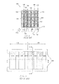
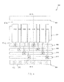
Figure 8 , aCCD 800 in accordance with an embodiment of the present invention includes gate electrodes H1S, H1B, H2S, and H2B disposed over a buried channel 802 (which in an embodiment is doped n-type). The H1S and H2S gate electrodes are high-voltage charge-multiplying electrodes in an embodiment in accordance with the invention. Thechannel 802 may be formed via, e.g., ion implantation. The heavily doped channel stops 804 (which are p-type for an n-type buried channel 802) are spaced away from the CCD gate electrodes and preferably also spaced away fromwires CCD 800; rather, the buriedchannel 802 confines such charge within theCCD 800. Furthermore, neither the CCD gate electrodes H1S, H1B, H2S, and H2B, nor any other gate electrodes, are disposed directly over the channel stops 804. The lateral distance between the channel stops 804 and thechannel 802 may be approximately 1 µm or greater, in order to substantially prevent generation of spurious charge within thechannel 802. - As shown in
Figure 8 , the channel stops 804 are spaced away from thechannel 802 by charge-depletedregions 814, which are fully depleted of charge carriers, at least during operation ofCCD 800. As utilized herein, "fully depleted" means substantially free of charge carriers (holes in the above exemplary embodiment) and/or including or consisting essentially of an electrically insulating material (e.g., a dielectric), at least during typical operation. A fully depleted region may have a relatively low doping level (and thus low level of charge carriers) when not in operation, but such carriers are easily removed from the region via, e.g., application of a moderate voltage. Since charge-depletedregions 814 are fully depleted, spurious charge generation via impact ionization at the interfaces ofchannel 802 therewith is substantially eliminated. The fully depleted regions may also extend below thechannel 802. The channel stops 804 may be formed via, e.g., ion implantation. As utilized herein, a "channel stop" is a region doped with a conductivity type opposite that of the channel and that is not fully depleted. For example, a channel stop may include or consist essentially of a well-defined region containing implanted dopants or a portion of a doped, non-depleted well having a conductivity type opposite that of the channel (e.g., a non-depleted p-well). In accordance with embodiments of the invention, channel stops may also be utilized as voltage references for the ground voltage (e.g., 0 V GND) against which other operating voltages are measured and defined. -
Figure 9 is a cross-sectional view along line B-B inFigure 8 . The p-type channel stops 804 and the n-type CCD buriedchannel 802 are disposed in a p-type well 900, which is formed over an n-type substrate 902. The p-type well 900 doping level is sufficiently low such that well 900 (at least charge-depletedregions 814 thereof) is fully depleted, at least when well 900 is held at 0 V and a positive voltage is applied to the n-type substrate 902. As mentioned above, the lack of charge carriers (holes in this example) substantially eliminates spurious charge generation in theCCD channel 802 when high voltages are applied to gate H1S. The charge in theCCD channel 802 is confined under the gate H1S by the n-type doping of theCCD channel 802, i.e., thechannel 802 is defined by the doping therein. In preferred embodiments of the invention, the channel stops 804 are not in contact with the n-type CCD channel 802. - In an embodiment of the invention, the wiring is arranged such that
wires wires channel stop 804 may be disposed underneath thewires 810 and/or 812. In various embodiments of the invention, the channel stops 804 are not continuous doped regions; rather, the channel stops may be formed as multiple dopedislands 816 separated by undoped or fully depletedregions 818, as illustrated for thelower channel stop 804 inFigure 8 . - The terms and expressions employed herein are used as terms and expressions of description and not of limitation, and there is no intention, in the use of such terms and expressions, of excluding any equivalents of the features shown and described or portions thereof. In addition, having described certain embodiments of the invention, it will be apparent to those of ordinary skill in the art that other embodiments incorporating the concepts disclosed herein may be used without departing from the spirit and scope of the invention. Accordingly, the described embodiments are to be considered in all respects as only illustrative and not restrictive.
Claims (14)
- A charge-coupled device (CCD) comprising:a channel for transfer of charge carriers therein, the channel having a first conductivity type;disposed over the channel, a plurality of gate electrodes for controlling transfer of charge carriers within the channel;laterally spaced away from opposite sides of the channel, first and second channel stops having a second conductivity type opposite the first conductivity type; anddisposed between the channel and each of the first and second channel stops, a fully depleted region.
- The CCD of claim 1, wherein at least one of the fully depleted regions extends beneath the channel.
- The CCD of claim 1, wherein (i) the CCD transfers charge carriers in multiple phases, and (ii) the plurality of gate electrodes comprises only one independently controllable gate electrode for each phase.
- The CCD of claim 1, wherein at least one of the plurality of gate electrodes is configured to multiply charge within the channel via application of a voltage larger than a voltage applied by at least one other gate electrode.
- The CCD of claim 1, wherein at least one of the first or second channel stops is a continuous doped region extending substantially along an entire length of the channel.
- The CCD of claim 1, wherein at least one of the first or second channel stops comprises a plurality of discrete and separated doped regions.
- The CCD of claim 1, further comprising a plurality of control wires each electrically connected to a gate electrode, wherein a horizontal distance between the channel and the second channel stop is less than a horizontal distance between the channel and at least one of the control wires.
- The CCD of claim 1, further comprising a plurality of control wires each electrically connected to a gate electrode, wherein a horizontal distance between the channel and the second channel stop is greater than a horizontal distance between the channel and the control wire disposed farthest from the channel.
- The CCD of claim 1, wherein the channel is disposed within a doped well of the second conductivity type.
- The CCD of claim 1, wherein each of the plurality of gate electrodes has a width larger than a width of the channel.
- A method of forming a charge-coupled device (CCD), the method comprising:forming a channel disposed within a substrate, the channel having a first conductivity type;forming, over the channel, a plurality of gate electrodes for controlling transfer of charge carriers within the channel; andforming, laterally spaced away from opposite sides of the channel, first and second channel stops having a second conductivity type opposite the first conductivity type,wherein the first and second channel stops are each spaced away from the channel by a fully depleted region.
- The method of claim 11, wherein forming the channel comprises ion implantation of dopants of the first conductivity type.
- The method of claim 11, wherein forming the first and second channel stops comprises ion implantation of dopants of the second conductivity type.
- The method of claim 11, wherein at least one of the plurality of gate electrodes is configured to multiply charge within the channel via application of a voltage larger than a voltage applied by at least one other gate electrode.
Applications Claiming Priority (2)
| Application Number | Priority Date | Filing Date | Title |
|---|---|---|---|
| US201161539123P | 2011-09-26 | 2011-09-26 | |
| US13/623,316 US8847285B2 (en) | 2011-09-26 | 2012-09-20 | Depleted charge-multiplying CCD image sensor |
Publications (3)
| Publication Number | Publication Date |
|---|---|
| EP2573816A2 true EP2573816A2 (en) | 2013-03-27 |
| EP2573816A3 EP2573816A3 (en) | 2014-05-07 |
| EP2573816B1 EP2573816B1 (en) | 2018-02-28 |
Family
ID=47143521
Family Applications (1)
| Application Number | Title | Priority Date | Filing Date |
|---|---|---|---|
| EP12186073.8A Not-in-force EP2573816B1 (en) | 2011-09-26 | 2012-09-26 | Depleted charge-multiplying CCD image sensor |
Country Status (3)
| Country | Link |
|---|---|
| US (2) | US8847285B2 (en) |
| EP (1) | EP2573816B1 (en) |
| JP (1) | JP6130639B2 (en) |
Cited By (1)
| Publication number | Priority date | Publication date | Assignee | Title |
|---|---|---|---|---|
| WO2017191475A1 (en) * | 2016-05-06 | 2017-11-09 | Teledyne E2V (Uk) Limited | Image sensor |
Families Citing this family (6)
| Publication number | Priority date | Publication date | Assignee | Title |
|---|---|---|---|---|
| US8847285B2 (en) * | 2011-09-26 | 2014-09-30 | Semiconductor Components Industries, Llc | Depleted charge-multiplying CCD image sensor |
| US11595595B2 (en) | 2016-09-27 | 2023-02-28 | Rxsafe Llc | Verification system for a pharmacy packaging system |
| US10187593B2 (en) | 2016-09-27 | 2019-01-22 | Rxsafe Llc | Verification system for a pharmacy packaging system |
| US10003688B1 (en) | 2018-02-08 | 2018-06-19 | Capital One Services, Llc | Systems and methods for cluster-based voice verification |
| CN111405210B (en) * | 2020-03-20 | 2022-01-28 | 中国电子科技集团公司第四十四研究所 | Pixel-level multiplication internal line frame transfer CCD pixel structure |
| US12134494B2 (en) | 2022-01-03 | 2024-11-05 | Rxsafe, Llc | Verification system for a pharmacy packaging system |
Citations (1)
| Publication number | Priority date | Publication date | Assignee | Title |
|---|---|---|---|---|
| US5337340A (en) | 1991-07-11 | 1994-08-09 | Texas Instruments Incorporated | Charge multiplying detector (CMD) suitable for small pixel CCD image sensors |
Family Cites Families (54)
| Publication number | Priority date | Publication date | Assignee | Title |
|---|---|---|---|---|
| JPS60244068A (en) * | 1984-05-18 | 1985-12-03 | Nec Corp | embedded channel charge coupled device |
| US4679212A (en) | 1984-07-31 | 1987-07-07 | Texas Instruments Incorporated | Method and apparatus for using surface trap recombination in solid state imaging devices |
| US5043819A (en) | 1989-12-05 | 1991-08-27 | Samsung Electronics Co., Ltd. | CCD solid state image sensor with two horizontal transfer CCDs corresponding to both odd and even columns of elements |
| JP2940034B2 (en) * | 1989-12-09 | 1999-08-25 | 日本電気株式会社 | Charge transfer device and method of manufacturing the same |
| US5250824A (en) | 1990-08-29 | 1993-10-05 | California Institute Of Technology | Ultra low-noise charge coupled device |
| JPH04260370A (en) * | 1991-02-14 | 1992-09-16 | Sony Corp | Solid-state image sensing device |
| KR100259063B1 (en) | 1992-06-12 | 2000-06-15 | 김영환 | CCD image device |
| US6288744B1 (en) * | 1994-11-11 | 2001-09-11 | Sanyo Electric Co., Ltd. | Solid-state image pickup device with a shared shift register and method of driving the same |
| KR0172854B1 (en) | 1995-08-02 | 1999-02-01 | 문정환 | CD solid state image pickup device and signal processing method thereof |
| US5708282A (en) | 1995-08-07 | 1998-01-13 | Q-Dot, Inc. | CCD charge splitter |
| US5693968A (en) | 1996-07-10 | 1997-12-02 | Board Of Supervisors Of Louisiana State University And Agricultural And Mechanical College | Bi-directional, fast-timing, charge coupled device |
| US6259085B1 (en) | 1996-11-01 | 2001-07-10 | The Regents Of The University Of California | Fully depleted back illuminated CCD |
| US5965910A (en) | 1997-04-29 | 1999-10-12 | Ohmeda Inc. | Large cell charge coupled device for spectroscopy |
| EP1099405B1 (en) | 1999-05-18 | 2005-08-03 | Olympus Corporation | Endoscope |
| US6278142B1 (en) | 1999-08-30 | 2001-08-21 | Isetex, Inc | Semiconductor image intensifier |
| US6680222B2 (en) | 1999-11-05 | 2004-01-20 | Isetex, Inc | Split-gate virtual-phase CCD image sensor with a diffused lateral overflow anti-blooming drain structure and process of making |
| JP4515617B2 (en) | 2000-10-23 | 2010-08-04 | 富士フイルム株式会社 | Solid-state imaging device and driving method thereof |
| US7139023B2 (en) | 2001-03-12 | 2006-11-21 | Texas Instruments Incorporated | High dynamic range charge readout system |
| US6784412B2 (en) | 2001-08-29 | 2004-08-31 | Texas Instruments Incorporated | Compact image sensor layout with charge multiplying register |
| US6624453B2 (en) | 2001-08-31 | 2003-09-23 | Eastman Kodak Company | Lateral overflow drain, anti-blooming structure for CCD devices having improved breakdown voltage |
| JP3689866B2 (en) | 2002-05-30 | 2005-08-31 | 日本テキサス・インスツルメンツ株式会社 | CMD and CCD device with CMD |
| ATE401666T1 (en) | 2002-09-19 | 2008-08-15 | Quantum Semiconductor Llc | LIGHT DETECTING DEVICE |
| JP2003333605A (en) * | 2003-04-25 | 2003-11-21 | Olympus Optical Co Ltd | Image pickup device |
| JP4343594B2 (en) | 2003-06-23 | 2009-10-14 | オリンパス株式会社 | Endoscope device |
| US20050029553A1 (en) | 2003-08-04 | 2005-02-10 | Jaroslav Hynecek | Clocked barrier virtual phase charge coupled device image sensor |
| US7078670B2 (en) | 2003-09-15 | 2006-07-18 | Imagerlabs, Inc. | Low noise charge gain circuit and CCD using same |
| US7233393B2 (en) | 2004-08-05 | 2007-06-19 | Applera Corporation | Signal noise reduction for imaging in biological analysis |
| GB2413007A (en) | 2004-04-07 | 2005-10-12 | E2V Tech Uk Ltd | Multiplication register for amplifying signal charge |
| EP1759526A2 (en) | 2004-05-28 | 2007-03-07 | Transoma Medical, Inc. | Method and device using ccd-based low noise parametric amplifier |
| US7352840B1 (en) | 2004-06-21 | 2008-04-01 | Radiation Monitoring Devices, Inc. | Micro CT scanners incorporating internal gain charge-coupled devices |
| US7692707B2 (en) | 2004-07-20 | 2010-04-06 | Shimadzu Corporation | Solid-state image pickup apparatus, image pickup apparatus, and image sensor |
| US7522205B2 (en) | 2004-09-10 | 2009-04-21 | Eastman Kodak Company | Image sensor with charge multiplication |
| WO2006038583A1 (en) | 2004-10-07 | 2006-04-13 | Shimadzu Corporation | Image pickup device, imaging apparatus using the same, and method for making image pickup device |
| CA2584186A1 (en) | 2004-10-18 | 2006-08-31 | Macquarie University | Fluorescence detection |
| GB0501149D0 (en) | 2005-01-20 | 2005-02-23 | Andor Technology Plc | Automatic calibration of electron multiplying CCds |
| US7271468B2 (en) * | 2005-02-16 | 2007-09-18 | The Regents Of The University Of California | High-voltage compatible, full-depleted CCD |
| JP2006261638A (en) | 2005-02-21 | 2006-09-28 | Sony Corp | Solid-state imaging device and driving method of solid-state imaging device |
| GB2431538B (en) | 2005-10-24 | 2010-12-22 | E2V Tech | CCD device |
| JP4358182B2 (en) | 2005-11-29 | 2009-11-04 | 株式会社日立国際電気 | Imaging apparatus and noise reduction method thereof |
| WO2008011617A2 (en) | 2006-07-21 | 2008-01-24 | The Regents Of The University Of California | Shallow-trench-isolation (sti)-bounded single-photon avalanche photodetectors |
| JP2008060550A (en) | 2006-07-31 | 2008-03-13 | Sanyo Electric Co Ltd | Imaging device |
| JP5037078B2 (en) | 2006-09-15 | 2012-09-26 | 富士フイルム株式会社 | Solid-state imaging device and driving method thereof |
| US7485840B2 (en) | 2007-02-08 | 2009-02-03 | Dalsa Corporation | Semiconductor charge multiplication amplifier device and semiconductor image sensor provided with such an amplifier device |
| US20080309808A1 (en) | 2007-06-18 | 2008-12-18 | Daisuke Kusuda | Method of driving ccd solid-state image pickup device, and image pickup apparatus |
| US8017917B2 (en) | 2007-10-29 | 2011-09-13 | The Board Of Trustees Of The University Of Illinois | Ionizing radiation sensor |
| JP5296406B2 (en) | 2008-04-02 | 2013-09-25 | パナソニック株式会社 | Solid-state imaging device and manufacturing method thereof |
| JP2010034512A (en) | 2008-07-01 | 2010-02-12 | Fujifilm Corp | Solid-state imaging element and imaging device |
| JP2010087366A (en) * | 2008-10-01 | 2010-04-15 | Kobe Steel Ltd | Metal powder for soft magnetic composite material, and soft magnetic composite material |
| JP5243983B2 (en) * | 2009-01-30 | 2013-07-24 | 浜松ホトニクス株式会社 | Solid-state image sensor with built-in electron multiplication function |
| EP2216817B1 (en) | 2009-02-05 | 2014-01-08 | STMicroelectronics (Crolles 2) SAS | Back side illuminated image sensor |
| JP5427541B2 (en) | 2009-10-08 | 2014-02-26 | 富士フイルム株式会社 | Solid-state imaging device, manufacturing method thereof, and imaging apparatus |
| US8294802B2 (en) | 2009-10-30 | 2012-10-23 | Truesense Imaging, Inc. | CCD image sensors having multiple lateral overflow drain regions for a horizontal shift register |
| US8773564B2 (en) | 2010-12-14 | 2014-07-08 | Truesense Imaging, Inc. | Image sensor with charge multiplication |
| US8847285B2 (en) * | 2011-09-26 | 2014-09-30 | Semiconductor Components Industries, Llc | Depleted charge-multiplying CCD image sensor |
-
2012
- 2012-09-20 US US13/623,316 patent/US8847285B2/en not_active Expired - Fee Related
- 2012-09-25 JP JP2012211191A patent/JP6130639B2/en not_active Expired - Fee Related
- 2012-09-26 EP EP12186073.8A patent/EP2573816B1/en not_active Not-in-force
-
2014
- 2014-04-01 US US14/231,839 patent/US9117729B2/en not_active Expired - Fee Related
Patent Citations (1)
| Publication number | Priority date | Publication date | Assignee | Title |
|---|---|---|---|---|
| US5337340A (en) | 1991-07-11 | 1994-08-09 | Texas Instruments Incorporated | Charge multiplying detector (CMD) suitable for small pixel CCD image sensors |
Cited By (1)
| Publication number | Priority date | Publication date | Assignee | Title |
|---|---|---|---|---|
| WO2017191475A1 (en) * | 2016-05-06 | 2017-11-09 | Teledyne E2V (Uk) Limited | Image sensor |
Also Published As
| Publication number | Publication date |
|---|---|
| EP2573816B1 (en) | 2018-02-28 |
| JP2013093562A (en) | 2013-05-16 |
| US20140231881A1 (en) | 2014-08-21 |
| JP6130639B2 (en) | 2017-05-17 |
| US20130075791A1 (en) | 2013-03-28 |
| US8847285B2 (en) | 2014-09-30 |
| US9117729B2 (en) | 2015-08-25 |
| EP2573816A3 (en) | 2014-05-07 |
Similar Documents
| Publication | Publication Date | Title |
|---|---|---|
| US12133006B2 (en) | Solid-state imaging device and imaging system | |
| US9117729B2 (en) | Depleted charge-multiplying CCD image sensor | |
| US8908070B2 (en) | Solid state imaging device and digital camera | |
| TWI359501B (en) | Solid-state imaging device and manufacturing metho | |
| JP6044044B2 (en) | Asymmetric gate matrix charge transfer image sensor | |
| JPH0271532A (en) | High dynamic range charge coupling device | |
| TWI521689B (en) | Multiple linear image sensor using charge integration | |
| JP2014063774A (en) | Solid-state imaging element, method of manufacturing the same, and camera | |
| JP2005057772A (en) | Virtual phase CCD image sensor with clocked barrier | |
| JP4777798B2 (en) | Solid-state imaging device and driving method thereof | |
| US7750376B2 (en) | Solid-state imaging device and imaging apparatus | |
| KR100545972B1 (en) | Solid state pickup device and driving method thereof | |
| JP2011054596A (en) | Ccd image sensor | |
| JP2010245177A (en) | Imaging device, imaging device manufacturing method, imaging device driving method, and imaging device | |
| JP3795808B2 (en) | Solid-state imaging device and imaging apparatus using the same | |
| JP2005101486A (en) | Solid-state imaging device and control method thereof | |
| KR100624341B1 (en) | Cassidi Solid State Imaging Device | |
| KR0155783B1 (en) | Charge coupled device solid state imaging device and method of manufacturing same | |
| JP4867309B2 (en) | Solid-state imaging device, manufacturing method thereof, and camera | |
| JP2003060188A (en) | Solid-state imaging device and driving method thereof | |
| JP4457570B2 (en) | Solid-state imaging device and manufacturing method thereof | |
| JP2010080791A (en) | Solid-state image sensing device and electronic instrument | |
| JP2002208692A (en) | Solid-state imaging device | |
| JP2006135172A (en) | Solid state image sensor and manufacturing method of same | |
| JP2007149758A (en) | Solid-state imaging device and manufacturing method thereof |
Legal Events
| Date | Code | Title | Description |
|---|---|---|---|
| PUAI | Public reference made under article 153(3) epc to a published international application that has entered the european phase |
Free format text: ORIGINAL CODE: 0009012 |
|
| AK | Designated contracting states |
Kind code of ref document: A2 Designated state(s): AL AT BE BG CH CY CZ DE DK EE ES FI FR GB GR HR HU IE IS IT LI LT LU LV MC MK MT NL NO PL PT RO RS SE SI SK SM TR |
|
| AX | Request for extension of the european patent |
Extension state: BA ME |
|
| PUAL | Search report despatched |
Free format text: ORIGINAL CODE: 0009013 |
|
| AK | Designated contracting states |
Kind code of ref document: A3 Designated state(s): AL AT BE BG CH CY CZ DE DK EE ES FI FR GB GR HR HU IE IS IT LI LT LU LV MC MK MT NL NO PL PT RO RS SE SI SK SM TR |
|
| AX | Request for extension of the european patent |
Extension state: BA ME |
|
| RIC1 | Information provided on ipc code assigned before grant |
Ipc: H01L 27/148 20060101AFI20140328BHEP |
|
| 17P | Request for examination filed |
Effective date: 20140923 |
|
| RBV | Designated contracting states (corrected) |
Designated state(s): AL AT BE BG CH CY CZ DE DK EE ES FI FR GB GR HR HU IE IS IT LI LT LU LV MC MK MT NL NO PL PT RO RS SE SI SK SM TR |
|
| RAP1 | Party data changed (applicant data changed or rights of an application transferred) |
Owner name: SEMICONDUCTOR COMPONENTS INDUSTRIES, LLC |
|
| RIN1 | Information on inventor provided before grant (corrected) |
Inventor name: SEMICONDUCTOR COMPONENTS INDUSTRIES, LLC |
|
| RIC1 | Information provided on ipc code assigned before grant |
Ipc: H01L 27/146 20060101ALI20170803BHEP Ipc: H01L 27/148 20060101AFI20170803BHEP |
|
| GRAP | Despatch of communication of intention to grant a patent |
Free format text: ORIGINAL CODE: EPIDOSNIGR1 |
|
| STAA | Information on the status of an ep patent application or granted ep patent |
Free format text: STATUS: GRANT OF PATENT IS INTENDED |
|
| RIN1 | Information on inventor provided before grant (corrected) |
Inventor name: PARKS, CHRISTOPHER |
|
| INTG | Intention to grant announced |
Effective date: 20170922 |
|
| GRAS | Grant fee paid |
Free format text: ORIGINAL CODE: EPIDOSNIGR3 |
|
| GRAA | (expected) grant |
Free format text: ORIGINAL CODE: 0009210 |
|
| STAA | Information on the status of an ep patent application or granted ep patent |
Free format text: STATUS: THE PATENT HAS BEEN GRANTED |
|
| AK | Designated contracting states |
Kind code of ref document: B1 Designated state(s): AL AT BE BG CH CY CZ DE DK EE ES FI FR GB GR HR HU IE IS IT LI LT LU LV MC MK MT NL NO PL PT RO RS SE SI SK SM TR |
|
| REG | Reference to a national code |
Ref country code: GB Ref legal event code: FG4D Ref country code: CH Ref legal event code: EP |
|
| REG | Reference to a national code |
Ref country code: AT Ref legal event code: REF Ref document number: 975024 Country of ref document: AT Kind code of ref document: T Effective date: 20180315 |
|
| REG | Reference to a national code |
Ref country code: IE Ref legal event code: FG4D |
|
| REG | Reference to a national code |
Ref country code: DE Ref legal event code: R096 Ref document number: 602012043304 Country of ref document: DE |
|
| REG | Reference to a national code |
Ref country code: NL Ref legal event code: MP Effective date: 20180228 |
|
| REG | Reference to a national code |
Ref country code: LT Ref legal event code: MG4D |
|
| REG | Reference to a national code |
Ref country code: AT Ref legal event code: MK05 Ref document number: 975024 Country of ref document: AT Kind code of ref document: T Effective date: 20180228 |
|
| PG25 | Lapsed in a contracting state [announced via postgrant information from national office to epo] |
Ref country code: NL Free format text: LAPSE BECAUSE OF FAILURE TO SUBMIT A TRANSLATION OF THE DESCRIPTION OR TO PAY THE FEE WITHIN THE PRESCRIBED TIME-LIMIT Effective date: 20180228 Ref country code: ES Free format text: LAPSE BECAUSE OF FAILURE TO SUBMIT A TRANSLATION OF THE DESCRIPTION OR TO PAY THE FEE WITHIN THE PRESCRIBED TIME-LIMIT Effective date: 20180228 Ref country code: LT Free format text: LAPSE BECAUSE OF FAILURE TO SUBMIT A TRANSLATION OF THE DESCRIPTION OR TO PAY THE FEE WITHIN THE PRESCRIBED TIME-LIMIT Effective date: 20180228 Ref country code: CY Free format text: LAPSE BECAUSE OF FAILURE TO SUBMIT A TRANSLATION OF THE DESCRIPTION OR TO PAY THE FEE WITHIN THE PRESCRIBED TIME-LIMIT Effective date: 20180228 Ref country code: FI Free format text: LAPSE BECAUSE OF FAILURE TO SUBMIT A TRANSLATION OF THE DESCRIPTION OR TO PAY THE FEE WITHIN THE PRESCRIBED TIME-LIMIT Effective date: 20180228 Ref country code: NO Free format text: LAPSE BECAUSE OF FAILURE TO SUBMIT A TRANSLATION OF THE DESCRIPTION OR TO PAY THE FEE WITHIN THE PRESCRIBED TIME-LIMIT Effective date: 20180528 Ref country code: HR Free format text: LAPSE BECAUSE OF FAILURE TO SUBMIT A TRANSLATION OF THE DESCRIPTION OR TO PAY THE FEE WITHIN THE PRESCRIBED TIME-LIMIT Effective date: 20180228 |
|
| REG | Reference to a national code |
Ref country code: FR Ref legal event code: PLFP Year of fee payment: 7 |
|
| PG25 | Lapsed in a contracting state [announced via postgrant information from national office to epo] |
Ref country code: RS Free format text: LAPSE BECAUSE OF FAILURE TO SUBMIT A TRANSLATION OF THE DESCRIPTION OR TO PAY THE FEE WITHIN THE PRESCRIBED TIME-LIMIT Effective date: 20180228 Ref country code: AT Free format text: LAPSE BECAUSE OF FAILURE TO SUBMIT A TRANSLATION OF THE DESCRIPTION OR TO PAY THE FEE WITHIN THE PRESCRIBED TIME-LIMIT Effective date: 20180228 Ref country code: GR Free format text: LAPSE BECAUSE OF FAILURE TO SUBMIT A TRANSLATION OF THE DESCRIPTION OR TO PAY THE FEE WITHIN THE PRESCRIBED TIME-LIMIT Effective date: 20180529 Ref country code: BG Free format text: LAPSE BECAUSE OF FAILURE TO SUBMIT A TRANSLATION OF THE DESCRIPTION OR TO PAY THE FEE WITHIN THE PRESCRIBED TIME-LIMIT Effective date: 20180528 Ref country code: SE Free format text: LAPSE BECAUSE OF FAILURE TO SUBMIT A TRANSLATION OF THE DESCRIPTION OR TO PAY THE FEE WITHIN THE PRESCRIBED TIME-LIMIT Effective date: 20180228 Ref country code: LV Free format text: LAPSE BECAUSE OF FAILURE TO SUBMIT A TRANSLATION OF THE DESCRIPTION OR TO PAY THE FEE WITHIN THE PRESCRIBED TIME-LIMIT Effective date: 20180228 |
|
| PG25 | Lapsed in a contracting state [announced via postgrant information from national office to epo] |
Ref country code: RO Free format text: LAPSE BECAUSE OF FAILURE TO SUBMIT A TRANSLATION OF THE DESCRIPTION OR TO PAY THE FEE WITHIN THE PRESCRIBED TIME-LIMIT Effective date: 20180228 Ref country code: IT Free format text: LAPSE BECAUSE OF FAILURE TO SUBMIT A TRANSLATION OF THE DESCRIPTION OR TO PAY THE FEE WITHIN THE PRESCRIBED TIME-LIMIT Effective date: 20180228 Ref country code: PL Free format text: LAPSE BECAUSE OF FAILURE TO SUBMIT A TRANSLATION OF THE DESCRIPTION OR TO PAY THE FEE WITHIN THE PRESCRIBED TIME-LIMIT Effective date: 20180228 Ref country code: EE Free format text: LAPSE BECAUSE OF FAILURE TO SUBMIT A TRANSLATION OF THE DESCRIPTION OR TO PAY THE FEE WITHIN THE PRESCRIBED TIME-LIMIT Effective date: 20180228 Ref country code: AL Free format text: LAPSE BECAUSE OF FAILURE TO SUBMIT A TRANSLATION OF THE DESCRIPTION OR TO PAY THE FEE WITHIN THE PRESCRIBED TIME-LIMIT Effective date: 20180228 |
|
| REG | Reference to a national code |
Ref country code: DE Ref legal event code: R097 Ref document number: 602012043304 Country of ref document: DE |
|
| PG25 | Lapsed in a contracting state [announced via postgrant information from national office to epo] |
Ref country code: SM Free format text: LAPSE BECAUSE OF FAILURE TO SUBMIT A TRANSLATION OF THE DESCRIPTION OR TO PAY THE FEE WITHIN THE PRESCRIBED TIME-LIMIT Effective date: 20180228 Ref country code: SK Free format text: LAPSE BECAUSE OF FAILURE TO SUBMIT A TRANSLATION OF THE DESCRIPTION OR TO PAY THE FEE WITHIN THE PRESCRIBED TIME-LIMIT Effective date: 20180228 Ref country code: DK Free format text: LAPSE BECAUSE OF FAILURE TO SUBMIT A TRANSLATION OF THE DESCRIPTION OR TO PAY THE FEE WITHIN THE PRESCRIBED TIME-LIMIT Effective date: 20180228 Ref country code: CZ Free format text: LAPSE BECAUSE OF FAILURE TO SUBMIT A TRANSLATION OF THE DESCRIPTION OR TO PAY THE FEE WITHIN THE PRESCRIBED TIME-LIMIT Effective date: 20180228 |
|
| PLBE | No opposition filed within time limit |
Free format text: ORIGINAL CODE: 0009261 |
|
| STAA | Information on the status of an ep patent application or granted ep patent |
Free format text: STATUS: NO OPPOSITION FILED WITHIN TIME LIMIT |
|
| 26N | No opposition filed |
Effective date: 20181129 |
|
| PG25 | Lapsed in a contracting state [announced via postgrant information from national office to epo] |
Ref country code: SI Free format text: LAPSE BECAUSE OF FAILURE TO SUBMIT A TRANSLATION OF THE DESCRIPTION OR TO PAY THE FEE WITHIN THE PRESCRIBED TIME-LIMIT Effective date: 20180228 |
|
| PG25 | Lapsed in a contracting state [announced via postgrant information from national office to epo] |
Ref country code: MC Free format text: LAPSE BECAUSE OF FAILURE TO SUBMIT A TRANSLATION OF THE DESCRIPTION OR TO PAY THE FEE WITHIN THE PRESCRIBED TIME-LIMIT Effective date: 20180228 |
|
| REG | Reference to a national code |
Ref country code: CH Ref legal event code: PL |
|
| REG | Reference to a national code |
Ref country code: BE Ref legal event code: MM Effective date: 20180930 |
|
| REG | Reference to a national code |
Ref country code: IE Ref legal event code: MM4A |
|
| PG25 | Lapsed in a contracting state [announced via postgrant information from national office to epo] |
Ref country code: LU Free format text: LAPSE BECAUSE OF NON-PAYMENT OF DUE FEES Effective date: 20180926 |
|
| PG25 | Lapsed in a contracting state [announced via postgrant information from national office to epo] |
Ref country code: IE Free format text: LAPSE BECAUSE OF NON-PAYMENT OF DUE FEES Effective date: 20180926 |
|
| PG25 | Lapsed in a contracting state [announced via postgrant information from national office to epo] |
Ref country code: CH Free format text: LAPSE BECAUSE OF NON-PAYMENT OF DUE FEES Effective date: 20180930 Ref country code: BE Free format text: LAPSE BECAUSE OF NON-PAYMENT OF DUE FEES Effective date: 20180930 Ref country code: LI Free format text: LAPSE BECAUSE OF NON-PAYMENT OF DUE FEES Effective date: 20180930 |
|
| PG25 | Lapsed in a contracting state [announced via postgrant information from national office to epo] |
Ref country code: MT Free format text: LAPSE BECAUSE OF NON-PAYMENT OF DUE FEES Effective date: 20180926 |
|
| PG25 | Lapsed in a contracting state [announced via postgrant information from national office to epo] |
Ref country code: TR Free format text: LAPSE BECAUSE OF FAILURE TO SUBMIT A TRANSLATION OF THE DESCRIPTION OR TO PAY THE FEE WITHIN THE PRESCRIBED TIME-LIMIT Effective date: 20180228 |
|
| PG25 | Lapsed in a contracting state [announced via postgrant information from national office to epo] |
Ref country code: PT Free format text: LAPSE BECAUSE OF FAILURE TO SUBMIT A TRANSLATION OF THE DESCRIPTION OR TO PAY THE FEE WITHIN THE PRESCRIBED TIME-LIMIT Effective date: 20180228 Ref country code: HU Free format text: LAPSE BECAUSE OF FAILURE TO SUBMIT A TRANSLATION OF THE DESCRIPTION OR TO PAY THE FEE WITHIN THE PRESCRIBED TIME-LIMIT; INVALID AB INITIO Effective date: 20120926 |
|
| PG25 | Lapsed in a contracting state [announced via postgrant information from national office to epo] |
Ref country code: MK Free format text: LAPSE BECAUSE OF NON-PAYMENT OF DUE FEES Effective date: 20180228 |
|
| PG25 | Lapsed in a contracting state [announced via postgrant information from national office to epo] |
Ref country code: IS Free format text: LAPSE BECAUSE OF FAILURE TO SUBMIT A TRANSLATION OF THE DESCRIPTION OR TO PAY THE FEE WITHIN THE PRESCRIBED TIME-LIMIT Effective date: 20180628 |
|
| PGFP | Annual fee paid to national office [announced via postgrant information from national office to epo] |
Ref country code: DE Payment date: 20200819 Year of fee payment: 9 Ref country code: GB Payment date: 20200819 Year of fee payment: 9 Ref country code: FR Payment date: 20200819 Year of fee payment: 9 |
|
| REG | Reference to a national code |
Ref country code: DE Ref legal event code: R119 Ref document number: 602012043304 Country of ref document: DE |
|
| GBPC | Gb: european patent ceased through non-payment of renewal fee |
Effective date: 20210926 |
|
| PG25 | Lapsed in a contracting state [announced via postgrant information from national office to epo] |
Ref country code: GB Free format text: LAPSE BECAUSE OF NON-PAYMENT OF DUE FEES Effective date: 20210926 Ref country code: FR Free format text: LAPSE BECAUSE OF NON-PAYMENT OF DUE FEES Effective date: 20210930 Ref country code: DE Free format text: LAPSE BECAUSE OF NON-PAYMENT OF DUE FEES Effective date: 20220401 |