EP2573769A1 - Variierende Morphologie in Magnetsensor-Unterschichten - Google Patents
Variierende Morphologie in Magnetsensor-Unterschichten Download PDFInfo
- Publication number
- EP2573769A1 EP2573769A1 EP12185310A EP12185310A EP2573769A1 EP 2573769 A1 EP2573769 A1 EP 2573769A1 EP 12185310 A EP12185310 A EP 12185310A EP 12185310 A EP12185310 A EP 12185310A EP 2573769 A1 EP2573769 A1 EP 2573769A1
- Authority
- EP
- European Patent Office
- Prior art keywords
- layer
- magnetic
- morphology
- sub
- layers
- Prior art date
- Legal status (The legal status is an assumption and is not a legal conclusion. Google has not performed a legal analysis and makes no representation as to the accuracy of the status listed.)
- Withdrawn
Links
Images


Classifications
-
- G—PHYSICS
- G11—INFORMATION STORAGE
- G11B—INFORMATION STORAGE BASED ON RELATIVE MOVEMENT BETWEEN RECORD CARRIER AND TRANSDUCER
- G11B5/00—Recording by magnetisation or demagnetisation of a record carrier; Reproducing by magnetic means; Record carriers therefor
- G11B5/127—Structure or manufacture of heads, e.g. inductive
- G11B5/33—Structure or manufacture of flux-sensitive heads, i.e. for reproduction only; Combination of such heads with means for recording or erasing only
- G11B5/39—Structure or manufacture of flux-sensitive heads, i.e. for reproduction only; Combination of such heads with means for recording or erasing only using magneto-resistive devices or effects
- G11B5/3903—Structure or manufacture of flux-sensitive heads, i.e. for reproduction only; Combination of such heads with means for recording or erasing only using magneto-resistive devices or effects using magnetic thin film layers or their effects, the films being part of integrated structures
- G11B5/3906—Details related to the use of magnetic thin film layers or to their effects
- G11B5/3929—Disposition of magnetic thin films not used for directly coupling magnetic flux from the track to the MR film or for shielding
- G11B5/3932—Magnetic biasing films
-
- B—PERFORMING OPERATIONS; TRANSPORTING
- B82—NANOTECHNOLOGY
- B82Y—SPECIFIC USES OR APPLICATIONS OF NANOSTRUCTURES; MEASUREMENT OR ANALYSIS OF NANOSTRUCTURES; MANUFACTURE OR TREATMENT OF NANOSTRUCTURES
- B82Y40/00—Manufacture or treatment of nanostructures
-
- G—PHYSICS
- G01—MEASURING; TESTING
- G01R—MEASURING ELECTRIC VARIABLES; MEASURING MAGNETIC VARIABLES
- G01R33/00—Arrangements or instruments for measuring magnetic variables
- G01R33/02—Measuring direction or magnitude of magnetic fields or magnetic flux
- G01R33/06—Measuring direction or magnitude of magnetic fields or magnetic flux using galvano-magnetic devices
- G01R33/09—Magnetoresistive devices
- G01R33/093—Magnetoresistive devices using multilayer structures, e.g. giant magnetoresistance sensors
-
- G—PHYSICS
- G11—INFORMATION STORAGE
- G11B—INFORMATION STORAGE BASED ON RELATIVE MOVEMENT BETWEEN RECORD CARRIER AND TRANSDUCER
- G11B5/00—Recording by magnetisation or demagnetisation of a record carrier; Reproducing by magnetic means; Record carriers therefor
- G11B5/127—Structure or manufacture of heads, e.g. inductive
- G11B5/31—Structure or manufacture of heads, e.g. inductive using thin films
- G11B5/3163—Fabrication methods or processes specially adapted for a particular head structure, e.g. using base layers for electroplating, using functional layers for masking, using energy or particle beams for shaping the structure or modifying the properties of the basic layers
-
- G—PHYSICS
- G11—INFORMATION STORAGE
- G11B—INFORMATION STORAGE BASED ON RELATIVE MOVEMENT BETWEEN RECORD CARRIER AND TRANSDUCER
- G11B5/00—Recording by magnetisation or demagnetisation of a record carrier; Reproducing by magnetic means; Record carriers therefor
- G11B5/127—Structure or manufacture of heads, e.g. inductive
- G11B5/33—Structure or manufacture of flux-sensitive heads, i.e. for reproduction only; Combination of such heads with means for recording or erasing only
- G11B5/39—Structure or manufacture of flux-sensitive heads, i.e. for reproduction only; Combination of such heads with means for recording or erasing only using magneto-resistive devices or effects
- G11B5/3903—Structure or manufacture of flux-sensitive heads, i.e. for reproduction only; Combination of such heads with means for recording or erasing only using magneto-resistive devices or effects using magnetic thin film layers or their effects, the films being part of integrated structures
- G11B5/3906—Details related to the use of magnetic thin film layers or to their effects
-
- H—ELECTRICITY
- H01—ELECTRIC ELEMENTS
- H01F—MAGNETS; INDUCTANCES; TRANSFORMERS; SELECTION OF MATERIALS FOR THEIR MAGNETIC PROPERTIES
- H01F10/00—Thin magnetic films, e.g. of one-domain structure
- H01F10/26—Thin magnetic films, e.g. of one-domain structure characterised by the substrate or intermediate layers
- H01F10/30—Thin magnetic films, e.g. of one-domain structure characterised by the substrate or intermediate layers characterised by the composition of the intermediate layers, e.g. seed, buffer, template, diffusion preventing, cap layers
-
- H—ELECTRICITY
- H01—ELECTRIC ELEMENTS
- H01F—MAGNETS; INDUCTANCES; TRANSFORMERS; SELECTION OF MATERIALS FOR THEIR MAGNETIC PROPERTIES
- H01F10/00—Thin magnetic films, e.g. of one-domain structure
- H01F10/32—Spin-exchange-coupled multilayers, e.g. nanostructured superlattices
- H01F10/324—Exchange coupling of magnetic film pairs via a very thin non-magnetic spacer, e.g. by exchange with conduction electrons of the spacer
- H01F10/3254—Exchange coupling of magnetic film pairs via a very thin non-magnetic spacer, e.g. by exchange with conduction electrons of the spacer the spacer being semiconducting or insulating, e.g. for spin tunnel junction [STJ]
-
- H—ELECTRICITY
- H01—ELECTRIC ELEMENTS
- H01F—MAGNETS; INDUCTANCES; TRANSFORMERS; SELECTION OF MATERIALS FOR THEIR MAGNETIC PROPERTIES
- H01F41/00—Apparatus or processes specially adapted for manufacturing or assembling magnets, inductances or transformers; Apparatus or processes specially adapted for manufacturing materials characterised by their magnetic properties
- H01F41/14—Apparatus or processes specially adapted for manufacturing or assembling magnets, inductances or transformers; Apparatus or processes specially adapted for manufacturing materials characterised by their magnetic properties for applying magnetic films to substrates
- H01F41/30—Apparatus or processes specially adapted for manufacturing or assembling magnets, inductances or transformers; Apparatus or processes specially adapted for manufacturing materials characterised by their magnetic properties for applying magnetic films to substrates for applying nanostructures, e.g. by molecular beam epitaxy [MBE]
- H01F41/302—Apparatus or processes specially adapted for manufacturing or assembling magnets, inductances or transformers; Apparatus or processes specially adapted for manufacturing materials characterised by their magnetic properties for applying magnetic films to substrates for applying nanostructures, e.g. by molecular beam epitaxy [MBE] for applying spin-exchange-coupled multilayers, e.g. nanostructured superlattices
- H01F41/303—Apparatus or processes specially adapted for manufacturing or assembling magnets, inductances or transformers; Apparatus or processes specially adapted for manufacturing materials characterised by their magnetic properties for applying magnetic films to substrates for applying nanostructures, e.g. by molecular beam epitaxy [MBE] for applying spin-exchange-coupled multilayers, e.g. nanostructured superlattices with exchange coupling adjustment of magnetic film pairs, e.g. interface modifications by reduction, oxidation
-
- Y—GENERAL TAGGING OF NEW TECHNOLOGICAL DEVELOPMENTS; GENERAL TAGGING OF CROSS-SECTIONAL TECHNOLOGIES SPANNING OVER SEVERAL SECTIONS OF THE IPC; TECHNICAL SUBJECTS COVERED BY FORMER USPC CROSS-REFERENCE ART COLLECTIONS [XRACs] AND DIGESTS
- Y10—TECHNICAL SUBJECTS COVERED BY FORMER USPC
- Y10T—TECHNICAL SUBJECTS COVERED BY FORMER US CLASSIFICATION
- Y10T428/00—Stock material or miscellaneous articles
- Y10T428/11—Magnetic recording head
- Y10T428/1107—Magnetoresistive
- Y10T428/1114—Magnetoresistive having tunnel junction effect
-
- Y—GENERAL TAGGING OF NEW TECHNOLOGICAL DEVELOPMENTS; GENERAL TAGGING OF CROSS-SECTIONAL TECHNOLOGIES SPANNING OVER SEVERAL SECTIONS OF THE IPC; TECHNICAL SUBJECTS COVERED BY FORMER USPC CROSS-REFERENCE ART COLLECTIONS [XRACs] AND DIGESTS
- Y10—TECHNICAL SUBJECTS COVERED BY FORMER USPC
- Y10T—TECHNICAL SUBJECTS COVERED BY FORMER US CLASSIFICATION
- Y10T428/00—Stock material or miscellaneous articles
- Y10T428/11—Magnetic recording head
- Y10T428/1107—Magnetoresistive
- Y10T428/1121—Multilayer
-
- Y—GENERAL TAGGING OF NEW TECHNOLOGICAL DEVELOPMENTS; GENERAL TAGGING OF CROSS-SECTIONAL TECHNOLOGIES SPANNING OVER SEVERAL SECTIONS OF THE IPC; TECHNICAL SUBJECTS COVERED BY FORMER USPC CROSS-REFERENCE ART COLLECTIONS [XRACs] AND DIGESTS
- Y10—TECHNICAL SUBJECTS COVERED BY FORMER USPC
- Y10T—TECHNICAL SUBJECTS COVERED BY FORMER US CLASSIFICATION
- Y10T428/00—Stock material or miscellaneous articles
- Y10T428/11—Magnetic recording head
- Y10T428/1107—Magnetoresistive
- Y10T428/1143—Magnetoresistive with defined structural feature
-
- Y—GENERAL TAGGING OF NEW TECHNOLOGICAL DEVELOPMENTS; GENERAL TAGGING OF CROSS-SECTIONAL TECHNOLOGIES SPANNING OVER SEVERAL SECTIONS OF THE IPC; TECHNICAL SUBJECTS COVERED BY FORMER USPC CROSS-REFERENCE ART COLLECTIONS [XRACs] AND DIGESTS
- Y10—TECHNICAL SUBJECTS COVERED BY FORMER USPC
- Y10T—TECHNICAL SUBJECTS COVERED BY FORMER US CLASSIFICATION
- Y10T428/00—Stock material or miscellaneous articles
- Y10T428/11—Magnetic recording head
- Y10T428/1171—Magnetic recording head with defined laminate structural detail
-
- Y—GENERAL TAGGING OF NEW TECHNOLOGICAL DEVELOPMENTS; GENERAL TAGGING OF CROSS-SECTIONAL TECHNOLOGIES SPANNING OVER SEVERAL SECTIONS OF THE IPC; TECHNICAL SUBJECTS COVERED BY FORMER USPC CROSS-REFERENCE ART COLLECTIONS [XRACs] AND DIGESTS
- Y10—TECHNICAL SUBJECTS COVERED BY FORMER USPC
- Y10T—TECHNICAL SUBJECTS COVERED BY FORMER US CLASSIFICATION
- Y10T428/00—Stock material or miscellaneous articles
- Y10T428/11—Magnetic recording head
- Y10T428/1193—Magnetic recording head with interlaminar component [e.g., adhesion layer, etc.]
Definitions
- a magnetic sensor can be constructed with a decoupling layer that has a predetermined first morphology.
- a magnetic free layer may be deposited contactingly adjacent to the decoupling layer with the magnetic free layer configured with at least a first sub-layer having a predetermined second morphology.
- an apparatus comprising:
- the decoupling layer has a first thickness and the first and second sub-layers respectively have second and third thicknesses.
- the second and third thicknesses are the same value.
- the second and third thicknesses are different values.
- the third thickness is 3 times greater than the second thickness.
- the decoupling layer is Tantalum.
- the decoupling layer is MgO.
- the first and second sub-layers are each a CoFeB alloy.
- the second morphology is substantially zero.
- the third morphology is substantially in a cross-track direction across the second sub-layer, the cross-track direction being substantially parallel to an air bearing surface of the magnetic free layer.
- the first angle is different from the second angle.
- the first and second angles with respect to a substrate plane that is perpendicular to an air bearing surface of each magnetic free sub-layer.
- the method further comprises annealing the first and second magnetic sub-layers to shift at least the third morphology a predetermined angular orientation.
- a sensor comprising a magnetically responsive stack biased to a predetermined default magnetization by a biasing magnet, the magnetically responsive stack having at least first and second magnetic free layers separated by a non-magnetic spacer layer, at least one magnetic free layer contactingly adjacent a decoupling layer having a first morphology, at least one magnetic free layer having first and second sub-layers respectively configured with second and third morphologies.
- the first and second magnetic free layers separated by the non-magnetic spacer layer are characterized as a trilayer magnetic element.
- the third morphology is tuned to correspond to a predetermined tunneling magnetoresistive ratio between the first and second magnetic free layers.
- the biasing magnet is formed on a seed layer configured with a fourth morphology.
- the biasing magnet is configured with at least two biasing sub-layers that each has a different morphology.
- the biasing magnet is configured with a fifth morphology that is different than the fourth morphology.
- a magnetic sensor with enhanced data sensing performance with variable morphologies is generally disclosed to meet heightened industry demand for larger data capacity and faster data transfer rates.
- Increasing data capacity may correspond to reduced form factors of various data storage components, such as read elements and shields.
- Such smaller magnetic components may have magnetic stability difficulties, particularly with precise shield-to-shield spacing criteria that can be demanded in high linear data density applications. Therefore, construction of reduced form factor magnetic sensor that can maintain magnetic orientation and sensitivity of a read element to enhance data sensing performance is in increasing demand in the industry.
- Such industry demand may be met by constructing a magnetic sensor with a decoupling layer contactingly adjacent a magnetic free layer that has first and second sub-layers that each have a morphology that differs from a morphology of the decoupling layer.
- the use of varying morphologies may provide elevated control of operational magnetizations of a magnetic stack that are influenced by pinned biasing magnetization.
- the ability to tune the various morphologies to elevate magnetization control can enhance data sensing by reducing magnetization asymmetry while improving magnetic stabilization and data signal amplitude.
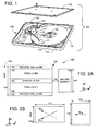
- FIG. 1 An exploded view of an embodiment of a data storage device 100 is generally provided in FIG. 1 in a non-limiting environment in which various embodiments of the present invention can be practiced.
- the device 100 includes a substantially sealed housing 102 formed from a base deck 104 and top cover 106.
- An internally disposed spindle motor 108 is configured to rotate a number of magnetic storage media 110.
- the media 110 are accessed by a corresponding array of data transducers (read/write heads) that are each supported by a head gimbal assembly (HGA) 112.
- HGA head gimbal assembly
- Each HGA 112 can be supported by a head-stack assembly 114 ("actuator") that includes a flexible suspension 116, which in turn is supported by a rigid actuator arm 118.
- the actuator 114 may pivot about a cartridge bearing assembly 120 through application of current to a voice coil motor (VCM) 122.
- VCM voice coil motor
- controlled operation of the VCM 122 causes the transducers (numerically denoted at 124) to align with tracks (not shown) defined on the media surfaces to store data thereto or retrieve data therefrom.
- FIGS. 2A and 2B display cross-section and top views, respectively, of block representations of an example magnetic sensor 130 capable of being used in various embodiments.
- the sensor 130 may be constructed with a magnetic stack 132 disposed between an air bearing surface 134 (ABS) and a rear biasing magnet 136.
- FIG. 2A illustrates how the magnetic stack 132 can be configured with a pair of magnetic free layers 138 separated by a non-magnetic spacer layer 140.
- the magnetic sensitivity of each free layer 138 can be tempered with decoupling layers 142 that can inhibit magnetic interference from reaching or escaping from the free layers 138 to an adjacent component, such as a magnetic shield.
- the stack 132 With the presence of magnetic free layers 138 without a fixed magnetization in the magnetic stack 132 to be used as a reference, the stack 132 can be characterized as a trilayer read element due to the dual free layers 138 and the spacer layer 140.
- a trilayer read element may utilize the rear biasing magnet 136 to impart a magnetic bias force on the free layers 138 and set a default magnetization, which allows accurate sensing of data bits across the ABS 134 in the absence of a pinned magnetization in the magnetic stack 132.
- a trilayer read element is displayed in the magnetic stack 132, construction of the stack 132 is not limited to such a configuration and can be a lamination of any number and type of layers with any magnetic orientation that is magnetically responsive.
- the magnetic sensor 130 may be tuned to operate with predetermined performance characteristics, such as signal amplitude and asymmetry, to sense data bits while minimizing the shield-to-shield spacing (SSS) 144 of the sensor 130.
- the magnetic sensor 130 can further be tuned by adjusting the dimensions and magnetizations of the stack 132 and biasing magnet 136, as displayed in top view of FIG. 2B .
- a biasing magnet thickness 146 and biasing distance 148 from the stack 132 can be adjusted to provide a predetermined amount of magnetic influence on the free layers 138, which may correspond to enhanced magnetization rotation and data sensing operation for the stack 132.
- the respective stack and biasing magnet widths 150 and 152 as measured parallel to the ABS along the Z axis, can be tuned to be similar or dissimilar and to correspond to respective stack and biasing magnet stripe heights 154 and 156.
- the width and stripe heights of the stack 132 and biasing magnet 136 can be tuned to provide a M PM magnetization of predetermined strength and angular orientation that influences the respective magnetic free layers 138 of the stack 132 to predetermined default magnetization configurations, M FL1 and M FL2 .
- the various dimensions, thicknesses, and magnetic orientations of the stack 132 and biasing magnet 136 can allow for adjustment and optimization to accommodate any number of predetermined operational and environmental conditions while maintaining a reduced form factor.
- accurate biasing of the stack 132, particularly reduced form factor stacks that include trilayer read elements, may be problematic as the free layers 138 lack direct contact to a set magnetization, such as M PM .
- FIG. 3 shows a cross-sectional block representation of a portion of an example magnetic stack 160 capable of being used in various embodiments.
- the stack 160 is constructed much like stack 132 of FIG. 2A with a magnetic free layer 162 disposed between and directly contacting a decoupling layer 164 and a non-magnetic spacer layer 166.
- the configuration of the various layers in the stack 160 is not limited to a particular design, but various embodiments combine a vapor deposited sub-layer, such as physical or chemical vapor deposition, with an obliquely deposited sub-layer to precisely control and tune morphology, which can reinforce the free layer 162 magnetization along predetermined default uniaxial directions, as displayed in FIG. 2B .
- a vapor deposited sub-layer such as physical or chemical vapor deposition
- an obliquely deposited sub-layer to precisely control and tune morphology, which can reinforce the free layer 162 magnetization along predetermined default uniaxial directions, as displayed in FIG. 2B .
- Such a configuration is displayed both in the decoupling layer 164 and the free layer 162 to allow individual morphologies that can correspond to unique predetermined magnetization behavior.
- the decoupling layer 164 has a decoupling VD sub-layer 168 that is deposited with a vapor deposition process that results in a predetermined first thickness 170 with minimal direction and strength.
- An oblique deposition process can then be undertaken to form the decoupling oblique sub-layer 172 with a predetermined second thickness 174 and designed morphology direction and strength that differ from the decoupling VD sub-layer 168.
- the combination of vapor and oblique deposition in subsequent sub-layers 168 and 172 can provide precise tuning of the overall morphology direction and strength in the magnetic layer. That is, the morphology of the entire decoupling layer 164 can be finely adjusted by tuning the thicknesses 170 and 174 of each sub-layer 168 and 172 to provide an overall morphology.
- the magnetic free layer 162 can also be formed with a free layer VD sub-layer 176 having a predetermined third thickness 178 directly coupled to a free layer oblique sub-layer 180 that has a predetermined fourth thickness 182.
- the free layer sub-layers 176 and 180 can have tuned thicknesses 178 and 182 that correspond with morphology directions and strengths that differ, but complement one another to provide enhanced magnetization retention and rotation in the presence of a sensed data bit.
- the order of the oblique deposition and standard deposition can be interchanged so that the obliquely deposited sub-layer 180 is contactingly adjacent the obliquely deposited decoupling sub-layer 172.
- FIG. 4 graphs morphologic behavior of example magnetic stacks having tuned oblique sub-layer percentage, which may correspond to the ratio of an obliquely deposited sub-layer thickness to an orthogonally deposited sub-layer thickness.
- Solid line 190 illustrates how overall morphology of a magnetic free layer can be tuned by adjusting not only the thickness of free layer sub-layers, but with the thicknesses of the decoupling sub-layers, such as sub-layer thicknesses 170 and 174 of FIG. 3 , which is displayed as a 20 ⁇ physical vapor deposition sub-layer thickness and a 20 ⁇ controlled incidence sputtering (CIS) sub-layer thickness.
- CIS controlled incidence sputtering
- segmented line 192 displays the morphologic behavior of a magnetic free layer with varying thickness formed atop a decoupling layer having a 30 ⁇ physical vapor deposition sub-layer thickness and a 10 ⁇ controlled incidence sputtering (CIS) sub-layer thickness. While a higher morphology strength may be obtained by solely forming the magnetic free layer with CIS, the ability to tune the morphology by successively depositing sub-layers with different morphologic strengths allows for a magnetic stack to be optimized for a wide variety of environmental and performance characteristics, such as high signal amplitude and magnetization stabilization.
- CIS controlled incidence sputtering
- the tuning and optimization of various aspects of a magnetic sensor are not limited to deposition techniques and thicknesses as a number of characteristics can further be adjusted to enhance sensor performance.
- One such characteristic is the deposition angle used for oblique deposition sub-layers, which may vary in some embodiments between 60° and 75° to provide predetermined morphology strength.
- Another deposition characteristic that can be tuned and optimized is the direction of incident oblique flux with respect to an underlying substrate (i.e. wafer fiducials) that can set the direction of the induced morphology with a predetermined plane of the substrate.
- Various embodiments can vary the sub-layer ordering, such as the oblique deposition of a sub-layer prior to the vapor deposited sub-layer, to control sensor operation and performance.
- Such variety of deposition characteristics and configurations that can be tuned may provide specific biasing magnetization schemes adapted to predetermined structural (form factor) and operational (sensing accuracy) criteria.
- FIG. 5 shows example configurations resultant to tuning of various aspects of a magnetic stack in accordance with various embodiments.
- Solid dots connected by solid line 200 illustrate how magnetic free layer thickness can affect a magnetic free layer sub-layer configuration tuned with an obliquely deposited decoupling layer made of Tantalum.
- the solid line 202 that connects hollow dots indicates the morphologic behavior of a magnetic free layer configuration tuned with a SiO 2 decoupling sub-layer.
- segmented line 204 corresponds to a Tantalum decoupling sub-layer having an 8nm thickness.
- the wide range of magnetic free layer thicknesses and morphology strengths can be utilized in a variety of different magnetic sensor configurations to provide optimized performance tuned specifically for various predetermined applications.
- the utilization of tuned sub-layers is not restricted to portions of the magnetic stack as the biasing magnet as well as leading, trailing, and side shields can likewise be formed with sub-layers that provide optimized biasing magnetization and enhanced data sensing performance.
- FIG. 6 generally illustrates a block representation of a cross-sectional view of a portion of an example magnetic sensor 210 that has a magnetic shield layer 212 deposited on an obliquely deposited seed sub-layer 214.
- the oblique depositions of the seed sub-layer 214 and shield layer 212 can be tuned with similar or dissimilar morphologies, which can be tuned by controlling the oblique angle of deposition, to provide enhanced magnetic stability for the shield layer 212 as the morphologies promotes tight magnetization dispersion throughout the shield layer 212.
- An obliquely deposited decoupling layer 216 is subsequently formed on the shield layer 212 with a predetermined stripe height 218 that can extend to any length along the sensor's stripe height 219.
- the stripe height 218 is distal to and separated from the ABS past the magnetic stack 220 at the rear biasing region 222 of the magnetic sensor 210 where the biasing magnet 224 can then be formed to utilize the predetermined morphology of the decoupling layer 216 to promote magnetic stability and consistent bias magnetization.
- deposition onto the decoupling layer 216 may provide improved magnetic stability in part due to the direct coupling therebetween.
- first and second magnetic free layers 226 and 228 are constructed with different sub-layer deposition orders that can tune magnetic sensor 210 performance by controlling the influence of the biasing magnet on default magnetizations of each free layer 226 and 228.
- the first magnetic free layer 226 has an obliquely deposited sub-layer 230 disposed between the decoupling layer 216 and a vapor deposited sub-layer 232 while the second magnetic free layer 228 has the opposite orientation as a vapor deposited sub-layer contacts both the non-magnetic spacer layer 234 and an obliquely deposited sub-layer 236.
- the various layer configurations shown in FIG. 6 can be individually or collectively deposited and tuned with predetermined morphologies that are arranged in various directions and range in strength from negligible to substantial, but form a cohesive magnetic sensor that exhibits optimized magnetic stability that may correspond with enhanced data sensing performance.
- FIG. 7 provides an example flowchart of a sensor fabrication routine 250 conducted in accordance with various embodiments to tune various portions of a magnetic sensor to provide predetermined optimized performance.
- the routine 250 begins by evaluating whether an oblique magnetic shield is to be included in the magnetic sensor in decision 252. If so, decision 254 determines if an oblique seed is to be formed prior to the deposition of the shield. Regardless of the deposition process chosen in decision 254, step 256 forms the seed layer either with minimal morphology that corresponds to vapor deposited layers or with a predetermined morphologic direction and strength associated with oblique deposition from a particular angle.
- step 256 With the seed layer formed in step 256, the shield layer is subsequently formed in step 258 with morphology that may or may not differ from that in the underlying seed layer.
- decision 260 evaluates if a decoupling layer is to be obliquely deposited which advances the routine 250 to decision 262 where the stripe height of the decoupling layer is determined.
- the deposition process is then utilized to form a decoupling layer with a predetermined stripe height and morphology in step 264. It can be appreciated that as a result of step 264 a decoupling layer may be configured like layer 216 of FIG. 6 or like layer 140 of FIG. 2A , either of which are tuned to designated morphologic criteria with the selection of the deposition technique and layer thickness.
- a rear biasing magnet is to be formed to impart bias magnetization that sets default magnetizations in the magnetic stack.
- Decision 266 and subsequent step 268 determine the tuned characteristics of the biasing magnet and construct the component in accordance with predetermined criteria.
- the magnetic stack portion of the magnetic sensor is next designed with decisions 270 and 272 determining the number, material, order, sub-layer thicknesses, and morphology characteristics of a magnetic free layer, which are then executed into a laminated magnetic free layer in step 274.
- decision 276 evaluates if a second free layer lamination is to be constructed. If so, a non-magnetic spacer layer is deposited in step 278 and the routine 250 returns to decision 270 where the second magnetic free layer is evaluated and the resultant design is implemented.
- routine 250 can be constructed from the routine 250 that exhibit various structural and operational characteristics, such as varying morphology, thicknesses, and bias magnetization influence.
- routine 250 is not limited only to the steps and decisions provided in FIG. 7 as any number of steps and determinations can be added, omitted, and modified to accommodate the fabrication of a precisely tuned magnetic sensor that utilizes varying morphology to provide enhanced magnetic data sensing.
- decision 266 and the corresponding formation of the biasing magnet in step 268 can be performed subsequent to the construction of the stack, which may include multiple sub-layers separated by the spacer layer.
- the configuration and material characteristics of the magnetic sensor described in the present disclosure allows for enhanced data reading performance during application in ever-decreasing form factor data storage devices.
- the use of varying morphologies can increase magnetic stability in the various pinned and free magnetic layers of a magnetic sensor.
- the ability to selectively tune the morphology by using sub-layers allows for precise control of magnetic sensor operation that corresponds with magnetizations optimized for particular environmental and operational behavior.
- the embodiments have been directed to magnetic sensing, it will be appreciated that the claimed invention can readily be utilized in any number of other applications, including data storage device applications.
Applications Claiming Priority (1)
| Application Number | Priority Date | Filing Date | Title |
|---|---|---|---|
| US13/239,010 US9036308B2 (en) | 2011-09-21 | 2011-09-21 | Varyinig morphology in magnetic sensor sub-layers |
Publications (1)
| Publication Number | Publication Date |
|---|---|
| EP2573769A1 true EP2573769A1 (de) | 2013-03-27 |
Family
ID=47221938
Family Applications (1)
| Application Number | Title | Priority Date | Filing Date |
|---|---|---|---|
| EP12185310A Withdrawn EP2573769A1 (de) | 2011-09-21 | 2012-09-20 | Variierende Morphologie in Magnetsensor-Unterschichten |
Country Status (4)
| Country | Link |
|---|---|
| US (1) | US9036308B2 (de) |
| EP (1) | EP2573769A1 (de) |
| JP (1) | JP5833992B2 (de) |
| CN (1) | CN103065644B (de) |
Cited By (1)
| Publication number | Priority date | Publication date | Assignee | Title |
|---|---|---|---|---|
| US9437229B2 (en) | 2014-04-09 | 2016-09-06 | Seagate Technology Llc | Isolator element for heat-assisted magnetic recording |
Families Citing this family (3)
| Publication number | Priority date | Publication date | Assignee | Title |
|---|---|---|---|---|
| US8912614B2 (en) * | 2011-11-11 | 2014-12-16 | International Business Machines Corporation | Magnetic tunnel junction devices having magnetic layers formed on composite, obliquely deposited seed layers |
| US8879214B2 (en) * | 2011-12-21 | 2014-11-04 | HGST Netherlands B.V. | Half metal trilayer TMR reader with negative interlayer coupling |
| US9349391B2 (en) | 2013-12-04 | 2016-05-24 | HGST Netherlands B.V. | Controlling magnetic layer anisotropy field by oblique angle static deposition |
Citations (6)
| Publication number | Priority date | Publication date | Assignee | Title |
|---|---|---|---|---|
| JPS5960725A (ja) * | 1982-09-29 | 1984-04-06 | Nec Corp | 磁気抵抗効果ヘツドの製造方法 |
| JPS59107417A (ja) * | 1982-12-13 | 1984-06-21 | Hitachi Ltd | 永久磁石バイアス型磁気抵抗効果磁気ヘツド |
| EP0581295A1 (de) * | 1992-07-31 | 1994-02-02 | Sony Corporation | Magnetoresistive Schicht und Verfahren zur ihrer Herstellung |
| US20030086217A1 (en) * | 1999-12-09 | 2003-05-08 | Mustafa Pinarbasi | Spin valve sensor free layer structure with a cobalt based layer that promotes magnetic stability and high magnetoresistance |
| US20090262465A1 (en) * | 2008-04-18 | 2009-10-22 | Masahiko Hatatani | Magnetic head and manufacturing method thereof |
| GB2474167A (en) * | 2008-06-20 | 2011-04-06 | Canon Anelva Corp | Method for manufacturing magnetoresistive device, sputter film-forming chamber, apparatus for manufacturing magnetoresistive device |
Family Cites Families (15)
| Publication number | Priority date | Publication date | Assignee | Title |
|---|---|---|---|---|
| US6937446B2 (en) * | 2000-10-20 | 2005-08-30 | Kabushiki Kaisha Toshiba | Magnetoresistance effect element, magnetic head and magnetic recording and/or reproducing system |
| US6847509B2 (en) * | 2001-02-01 | 2005-01-25 | Kabushiki Kaisha Toshiba | Magnetoresistive head and perpendicular magnetic recording-reproducing apparatus |
| US6667862B2 (en) * | 2001-02-20 | 2003-12-23 | Carnegie Mellon University | Magnetoresistive read head having permanent magnet on top of magnetoresistive element |
| US7035062B1 (en) * | 2001-11-29 | 2006-04-25 | Seagate Technology Llc | Structure to achieve sensitivity and linear density in tunneling GMR heads using orthogonal magnetic alignments |
| US6818961B1 (en) | 2003-06-30 | 2004-11-16 | Freescale Semiconductor, Inc. | Oblique deposition to induce magnetic anisotropy for MRAM cells |
| US20050066897A1 (en) | 2003-09-29 | 2005-03-31 | Seagate Technology Llc | System, method and aperture for oblique deposition |
| US7061731B2 (en) | 2003-11-17 | 2006-06-13 | Seagate Technology Llc | High magnetic anisotropy hard magnetic bias element |
| US6992359B2 (en) * | 2004-02-26 | 2006-01-31 | Grandis, Inc. | Spin transfer magnetic element with free layers having high perpendicular anisotropy and in-plane equilibrium magnetization |
| US7436637B2 (en) * | 2005-10-05 | 2008-10-14 | Hitachi Global Storage Technologies Netherlands B.V. | Magnetoresistive sensor having an improved pinning structure |
| JP4444241B2 (ja) * | 2005-10-19 | 2010-03-31 | 株式会社東芝 | 磁気抵抗効果素子、磁気ランダムアクセスメモリ、電子カード及び電子装置 |
| US7916429B2 (en) * | 2007-07-30 | 2011-03-29 | Tdk Corporation | Magnetic field detecting element having thin stack with a plurality of free layers and thick bias magnetic layer |
| US8099855B2 (en) | 2007-12-16 | 2012-01-24 | Hitachi Global Storage Technologies Netherlands, B.V. | Methods for fabricating perpendicular recording heads with controlled separation regions |
| US8077436B2 (en) | 2008-03-20 | 2011-12-13 | Tdk Corporation | CPP-type magnetoresistance effect element having three magnetic layers |
| JP5529648B2 (ja) | 2009-08-04 | 2014-06-25 | キヤノンアネルバ株式会社 | 磁気センサ積層体、その成膜方法、成膜制御プログラムおよび記録媒体 |
| US8130475B2 (en) * | 2009-10-20 | 2012-03-06 | Tdk Corporation | Method for manufacturing CPP-type thin film magnetic head provided with a pair of magnetically free layers |
-
2011
- 2011-09-21 US US13/239,010 patent/US9036308B2/en active Active
-
2012
- 2012-09-20 JP JP2012206842A patent/JP5833992B2/ja not_active Expired - Fee Related
- 2012-09-20 EP EP12185310A patent/EP2573769A1/de not_active Withdrawn
- 2012-09-21 CN CN201210478643.8A patent/CN103065644B/zh not_active Expired - Fee Related
Patent Citations (6)
| Publication number | Priority date | Publication date | Assignee | Title |
|---|---|---|---|---|
| JPS5960725A (ja) * | 1982-09-29 | 1984-04-06 | Nec Corp | 磁気抵抗効果ヘツドの製造方法 |
| JPS59107417A (ja) * | 1982-12-13 | 1984-06-21 | Hitachi Ltd | 永久磁石バイアス型磁気抵抗効果磁気ヘツド |
| EP0581295A1 (de) * | 1992-07-31 | 1994-02-02 | Sony Corporation | Magnetoresistive Schicht und Verfahren zur ihrer Herstellung |
| US20030086217A1 (en) * | 1999-12-09 | 2003-05-08 | Mustafa Pinarbasi | Spin valve sensor free layer structure with a cobalt based layer that promotes magnetic stability and high magnetoresistance |
| US20090262465A1 (en) * | 2008-04-18 | 2009-10-22 | Masahiko Hatatani | Magnetic head and manufacturing method thereof |
| GB2474167A (en) * | 2008-06-20 | 2011-04-06 | Canon Anelva Corp | Method for manufacturing magnetoresistive device, sputter film-forming chamber, apparatus for manufacturing magnetoresistive device |
Cited By (1)
| Publication number | Priority date | Publication date | Assignee | Title |
|---|---|---|---|---|
| US9437229B2 (en) | 2014-04-09 | 2016-09-06 | Seagate Technology Llc | Isolator element for heat-assisted magnetic recording |
Also Published As
| Publication number | Publication date |
|---|---|
| CN103065644A (zh) | 2013-04-24 |
| US9036308B2 (en) | 2015-05-19 |
| JP5833992B2 (ja) | 2015-12-16 |
| JP2013069401A (ja) | 2013-04-18 |
| CN103065644B (zh) | 2016-12-21 |
| US20130071692A1 (en) | 2013-03-21 |
Similar Documents
| Publication | Publication Date | Title |
|---|---|---|
| US8582249B2 (en) | Magnetic element with reduced shield-to-shield spacing | |
| US9165574B2 (en) | Magnetic element with dual magnetic moments | |
| US8760820B1 (en) | Magnetic element with coupled side shield | |
| US8582247B2 (en) | Magnetic element with increased scissoring angle | |
| US9165570B2 (en) | Data reader with magnetic seed lamination | |
| US10147447B2 (en) | Magnetic element with reduced shield-to-shield spacing | |
| US8675315B2 (en) | Magnetic sensor with anisotropic liner | |
| US8503135B2 (en) | Magnetic sensor with enhanced magnetoresistance ratio | |
| US8755154B2 (en) | Tuned angled uniaxial anisotropy in trilayer magnetic sensors | |
| US20130069642A1 (en) | Magnetic Sensor With Conducting Bevel | |
| US8470463B2 (en) | Magnetic shield with in-plane anisotropy | |
| US9036308B2 (en) | Varyinig morphology in magnetic sensor sub-layers | |
| US8896971B2 (en) | Aligned magnetic insulating feature | |
| EP2728579B1 (de) | Magnetisches Element mit Stromkonstriktionsmerkmal | |
| US8749924B2 (en) | Tuned shunt ratio for magnetic sensors | |
| US8737023B2 (en) | Magnetic reader with tuned anisotropy | |
| US9240200B2 (en) | Magnetic element with crossed anisotropies | |
| US20080112091A1 (en) | Current-confined-path type magnetoresistive element and method of manufacturing same | |
| US9218826B1 (en) | Tuned horizontally symmetric magnetic stack |
Legal Events
| Date | Code | Title | Description |
|---|---|---|---|
| PUAI | Public reference made under article 153(3) epc to a published international application that has entered the european phase |
Free format text: ORIGINAL CODE: 0009012 |
|
| AK | Designated contracting states |
Kind code of ref document: A1 Designated state(s): AL AT BE BG CH CY CZ DE DK EE ES FI FR GB GR HR HU IE IS IT LI LT LU LV MC MK MT NL NO PL PT RO RS SE SI SK SM TR |
|
| AX | Request for extension of the european patent |
Extension state: BA ME |
|
| 17P | Request for examination filed |
Effective date: 20130927 |
|
| RBV | Designated contracting states (corrected) |
Designated state(s): AL AT BE BG CH CY CZ DE DK EE ES FI FR GB GR HR HU IE IS IT LI LT LU LV MC MK MT NL NO PL PT RO RS SE SI SK SM TR |
|
| 17Q | First examination report despatched |
Effective date: 20170623 |
|
| STAA | Information on the status of an ep patent application or granted ep patent |
Free format text: STATUS: THE APPLICATION IS DEEMED TO BE WITHDRAWN |
|
| 18D | Application deemed to be withdrawn |
Effective date: 20190402 |