EP2570412B1 - Novel nitrogen-containing heterocyclic compound and organic electronic device using the same - Google Patents
Novel nitrogen-containing heterocyclic compound and organic electronic device using the same Download PDFInfo
- Publication number
- EP2570412B1 EP2570412B1 EP12190141.7A EP12190141A EP2570412B1 EP 2570412 B1 EP2570412 B1 EP 2570412B1 EP 12190141 A EP12190141 A EP 12190141A EP 2570412 B1 EP2570412 B1 EP 2570412B1
- Authority
- EP
- European Patent Office
- Prior art keywords
- group
- compound
- substituted
- unsubstituted
- organic
- Prior art date
- Legal status (The legal status is an assumption and is not a legal conclusion. Google has not performed a legal analysis and makes no representation as to the accuracy of the status listed.)
- Active
Links
- 0 CC(C1*)C=C1c1cc(-c2c(-c3ccccc3)nc3[n]2c2ccccc2c2cc(-c4ccccc4)ccc32)ccc1 Chemical compound CC(C1*)C=C1c1cc(-c2c(-c3ccccc3)nc3[n]2c2ccccc2c2cc(-c4ccccc4)ccc32)ccc1 0.000 description 13
- OVUGJXBLYMJIQE-UHFFFAOYSA-N c(cc1)ccc1-c(cc1c2c3cccc2)ccc1[n]1c3nc2c1c(cccc1)c1c1c2cccc1 Chemical compound c(cc1)ccc1-c(cc1c2c3cccc2)ccc1[n]1c3nc2c1c(cccc1)c1c1c2cccc1 OVUGJXBLYMJIQE-UHFFFAOYSA-N 0.000 description 2
- KYKPZLIIBCNVEK-UHFFFAOYSA-N c(cc1)ccc1-c1ccc(c2nc(c(cccc3)c3c3c4cccc3)c4[n]2c(c2c3)ccc3-c3ccccc3)c2c1 Chemical compound c(cc1)ccc1-c1ccc(c2nc(c(cccc3)c3c3c4cccc3)c4[n]2c(c2c3)ccc3-c3ccccc3)c2c1 KYKPZLIIBCNVEK-UHFFFAOYSA-N 0.000 description 2
- CPDNSGUWEUZWNO-UHFFFAOYSA-N c(ccc1c(cccc2)c2c2nc3c(cccc4)c4c4c5)cc1c2[n]3c4ccc5-c1ccc(cc2)c3c1ccc1c3c2ccc1 Chemical compound c(ccc1c(cccc2)c2c2nc3c(cccc4)c4c4c5)cc1c2[n]3c4ccc5-c1ccc(cc2)c3c1ccc1c3c2ccc1 CPDNSGUWEUZWNO-UHFFFAOYSA-N 0.000 description 2
- XSDKKRKTDZMKCH-UHFFFAOYSA-N Brc(cc1)ccc1-[n]1c2ccccc2c2ccccc12 Chemical compound Brc(cc1)ccc1-[n]1c2ccccc2c2ccccc12 XSDKKRKTDZMKCH-UHFFFAOYSA-N 0.000 description 1
- BKXPNVMULXFPOY-UHFFFAOYSA-N Brc(cc1)ccc1-c1nc(c(cccc2)c2cc2)c2cc1 Chemical compound Brc(cc1)ccc1-c1nc(c(cccc2)c2cc2)c2cc1 BKXPNVMULXFPOY-UHFFFAOYSA-N 0.000 description 1
- PDRHKHRFNRUHIQ-CQPUUCJISA-N C/C=C\c1cc(-c2c(cccc3)c3c(-c3cc(cccc4)c4cc3)c3c2ccc(-c(cc2)ccc2-c(cc2c4c5cccc4)ccc2[n]2c5nc4c(cccc5)c5c(cccc5)c5c24)c3)ccc1C=C Chemical compound C/C=C\c1cc(-c2c(cccc3)c3c(-c3cc(cccc4)c4cc3)c3c2ccc(-c(cc2)ccc2-c(cc2c4c5cccc4)ccc2[n]2c5nc4c(cccc5)c5c(cccc5)c5c24)c3)ccc1C=C PDRHKHRFNRUHIQ-CQPUUCJISA-N 0.000 description 1
- HBAYVSITUFARGI-UHFFFAOYSA-N C1=CC(c2ccccc2)=CC2c3ccccc3-c3nc(-c4ccccc4)c(-c4ccccc4)[n]3C12 Chemical compound C1=CC(c2ccccc2)=CC2c3ccccc3-c3nc(-c4ccccc4)c(-c4ccccc4)[n]3C12 HBAYVSITUFARGI-UHFFFAOYSA-N 0.000 description 1
- ZILFDKNBNDDFTL-UHFFFAOYSA-N C1C2SC=NC2C=CC1 Chemical compound C1C2SC=NC2C=CC1 ZILFDKNBNDDFTL-UHFFFAOYSA-N 0.000 description 1
- ONUOKKOEOWFWGO-UHFFFAOYSA-N C1N(c2ccccc2)c2ccccc2-c2c1ccc(-c(cc1c3ccccc33)ccc1[n]1c3nc3c1c1ccccc1c1ccccc31)c2 Chemical compound C1N(c2ccccc2)c2ccccc2-c2c1ccc(-c(cc1c3ccccc33)ccc1[n]1c3nc3c1c1ccccc1c1ccccc31)c2 ONUOKKOEOWFWGO-UHFFFAOYSA-N 0.000 description 1
- XBGFWLBQKQIBFN-QCXCKAPVSA-N CC(/C=C\c1c(C)c(cccc2)c2c2nc(c3ccccc3c3ccccc33)c3[n]12)c(cc1)ccc1N(/C(/C=C)=C/C=C(\C)/c1ccccc1)c(cc1)ccc1-c1ccccc1 Chemical compound CC(/C=C\c1c(C)c(cccc2)c2c2nc(c3ccccc3c3ccccc33)c3[n]12)c(cc1)ccc1N(/C(/C=C)=C/C=C(\C)/c1ccccc1)c(cc1)ccc1-c1ccccc1 XBGFWLBQKQIBFN-QCXCKAPVSA-N 0.000 description 1
- GWUZFINDQOKKPF-UHFFFAOYSA-N CC(C1C=C2)(C=C2c(cc2)ccc2-c2ccccc2)c2nc(-c(cc3)ccc3C#N)c(-c3ccc(C)cc3)[n]2-c2c1cccc2 Chemical compound CC(C1C=C2)(C=C2c(cc2)ccc2-c2ccccc2)c2nc(-c(cc3)ccc3C#N)c(-c3ccc(C)cc3)[n]2-c2c1cccc2 GWUZFINDQOKKPF-UHFFFAOYSA-N 0.000 description 1
- RTNOPCIBGFYBEI-UHFFFAOYSA-N CC(c(cc1)ccc1[Br]=C)=O Chemical compound CC(c(cc1)ccc1[Br]=C)=O RTNOPCIBGFYBEI-UHFFFAOYSA-N 0.000 description 1
- OQCJJPATWQSHIN-WZUFQYTHSA-N Cc(cc1)ccc1-c1c(-c(cc2)ccc2C#N)nc(c2c3)[n]1c(C)c(/C=C\C=C)c2ccc3-c(cc1)ccc1-c1ccccc1 Chemical compound Cc(cc1)ccc1-c1c(-c(cc2)ccc2C#N)nc(c2c3)[n]1c(C)c(/C=C\C=C)c2ccc3-c(cc1)ccc1-c1ccccc1 OQCJJPATWQSHIN-WZUFQYTHSA-N 0.000 description 1
- DZGNOAZYFZEJFR-UHFFFAOYSA-N Cc1ccc(-c(cc2)ccc2-c(cc2)cc(c3ccccc33)c2[n]2c3nc3c2c2ccccc2c2ccccc32)[s]1 Chemical compound Cc1ccc(-c(cc2)ccc2-c(cc2)cc(c3ccccc33)c2[n]2c3nc3c2c2ccccc2c2ccccc32)[s]1 DZGNOAZYFZEJFR-UHFFFAOYSA-N 0.000 description 1
- MBCBVLMTEBQORF-UHFFFAOYSA-N N#Cc(cc1)ccc1-c1c(-c(cc2)ccc2C#N)nc(c(cccc2)c2c2c3)[n]1c2ccc3-c(cc1)ccc1-c1ccccc1 Chemical compound N#Cc(cc1)ccc1-c1c(-c(cc2)ccc2C#N)nc(c(cccc2)c2c2c3)[n]1c2ccc3-c(cc1)ccc1-c1ccccc1 MBCBVLMTEBQORF-UHFFFAOYSA-N 0.000 description 1
- DQMWRYNESQUIED-UHFFFAOYSA-N N#Cc(cc1)ccc1-c1c(-c(cc2)ccc2C#N)nc(c2c3)[n]1c(cccc1)c1c2ccc3-c(cc1)ccc1C1=CC2=CC=CCC2C=C1 Chemical compound N#Cc(cc1)ccc1-c1c(-c(cc2)ccc2C#N)nc(c2c3)[n]1c(cccc1)c1c2ccc3-c(cc1)ccc1C1=CC2=CC=CCC2C=C1 DQMWRYNESQUIED-UHFFFAOYSA-N 0.000 description 1
- GCUCLENTKXXYCX-UHFFFAOYSA-N N#Cc(cc1)ccc1-c1c(-c(cc2)ccc2C#N)nc(c2c3)[n]1c(cccc1)c1c2ccc3-c1nc(-c2ccccn2)ccc1 Chemical compound N#Cc(cc1)ccc1-c1c(-c(cc2)ccc2C#N)nc(c2c3)[n]1c(cccc1)c1c2ccc3-c1nc(-c2ccccn2)ccc1 GCUCLENTKXXYCX-UHFFFAOYSA-N 0.000 description 1
- QLLIRARUVCBXGV-UHFFFAOYSA-N N#Cc(cc1)ccc1-c1c(-c(cc2)ccc2C#N)nc(c2c3)[n]1c1ccccc1c2ccc3-c(cc1)ccc1-c1ccccn1 Chemical compound N#Cc(cc1)ccc1-c1c(-c(cc2)ccc2C#N)nc(c2c3)[n]1c1ccccc1c2ccc3-c(cc1)ccc1-c1ccccn1 QLLIRARUVCBXGV-UHFFFAOYSA-N 0.000 description 1
- SAUQRZGFTZCLRM-UHFFFAOYSA-N N#Cc(cc1)ccc1-c1c(-c(cc2)ccc2C#N)nc-2[n]1C1C=CC=CC1c1c-2ccc(-c(cc2)ccc2-c2ccc(cccc3)c3c2)c1 Chemical compound N#Cc(cc1)ccc1-c1c(-c(cc2)ccc2C#N)nc-2[n]1C1C=CC=CC1c1c-2ccc(-c(cc2)ccc2-c2ccc(cccc3)c3c2)c1 SAUQRZGFTZCLRM-UHFFFAOYSA-N 0.000 description 1
- UKIRZNBBBBFMSX-UHFFFAOYSA-N N#Cc(cc1)ccc1-c1c(-c(cc2)ccc2C#N)nc2[n]1c1ccccc1c1c2ccc(-c(cc2)ccc2-c2cc3ccccc3cc2)c1 Chemical compound N#Cc(cc1)ccc1-c1c(-c(cc2)ccc2C#N)nc2[n]1c1ccccc1c1c2ccc(-c(cc2)ccc2-c2cc3ccccc3cc2)c1 UKIRZNBBBBFMSX-UHFFFAOYSA-N 0.000 description 1
- JIDPUOUTMXBVQI-UHFFFAOYSA-N N#Cc(cc1)ccc1-c1c(-c(cc2)ccc2C#N)nc2[n]1c1ccccc1c1c2ccc(-c2ccc(cc(cc3)-c4cc(cccc5)c5cc4)c3c2)c1 Chemical compound N#Cc(cc1)ccc1-c1c(-c(cc2)ccc2C#N)nc2[n]1c1ccccc1c1c2ccc(-c2ccc(cc(cc3)-c4cc(cccc5)c5cc4)c3c2)c1 JIDPUOUTMXBVQI-UHFFFAOYSA-N 0.000 description 1
- QPRPQMYNMVEVKZ-UHFFFAOYSA-N N#Cc1ccc(C(C23)C2(c(cc2)ccc2C#N)N=C2N3c(cccc3)c3C(C=C3)=C2CC3c2ccc(cc(cc3)C4=CC5=CCCC=C5C=C4)c3c2)cc1 Chemical compound N#Cc1ccc(C(C23)C2(c(cc2)ccc2C#N)N=C2N3c(cccc3)c3C(C=C3)=C2CC3c2ccc(cc(cc3)C4=CC5=CCCC=C5C=C4)c3c2)cc1 QPRPQMYNMVEVKZ-UHFFFAOYSA-N 0.000 description 1
- DKHNGUNXLDCATP-UHFFFAOYSA-N N#Cc1nc(c(nc2C#N)c(c(nc3C#N)c4nc3C#N)nc2C#N)c4nc1C#N Chemical compound N#Cc1nc(c(nc2C#N)c(c(nc3C#N)c4nc3C#N)nc2C#N)c4nc1C#N DKHNGUNXLDCATP-UHFFFAOYSA-N 0.000 description 1
- WDFQBORIUYODSI-UHFFFAOYSA-N Nc(cc1)ccc1Br Chemical compound Nc(cc1)ccc1Br WDFQBORIUYODSI-UHFFFAOYSA-N 0.000 description 1
- NZGWBDGBNINXJY-UHFFFAOYSA-N Nc1c(C=O)ccc2c1cccc2 Chemical compound Nc1c(C=O)ccc2c1cccc2 NZGWBDGBNINXJY-UHFFFAOYSA-N 0.000 description 1
- XPEIJWZLPWNNOK-UHFFFAOYSA-N OB(c(cc1)ccc1-c1ccccc1)O Chemical compound OB(c(cc1)ccc1-c1ccccc1)O XPEIJWZLPWNNOK-UHFFFAOYSA-N 0.000 description 1
- KGCHZMXLCFQXAR-UHFFFAOYSA-N c(cc1)cc(cc2)c1cc2-c1c(cccc2)c2c(-c2c(cccc3)c3ccc2)c(cc2)c1cc2-c(cc1)cc2c1c1nc(c(cccc3)c3c3c4cccc3)c4[n]1c1c2cccc1 Chemical compound c(cc1)cc(cc2)c1cc2-c1c(cccc2)c2c(-c2c(cccc3)c3ccc2)c(cc2)c1cc2-c(cc1)cc2c1c1nc(c(cccc3)c3c3c4cccc3)c4[n]1c1c2cccc1 KGCHZMXLCFQXAR-UHFFFAOYSA-N 0.000 description 1
- HXACEJSYXPFOAL-UHFFFAOYSA-N c(cc1)cc(cc2)c1cc2-c1c(cccc2)c2c(-c2c(cccc3)c3ccc2)c(cc2)c1cc2-c(cc1c2ccccc22)ccc1[n]1c2nc2c(cccc3)c3c(cccc3)c3c12 Chemical compound c(cc1)cc(cc2)c1cc2-c1c(cccc2)c2c(-c2c(cccc3)c3ccc2)c(cc2)c1cc2-c(cc1c2ccccc22)ccc1[n]1c2nc2c(cccc3)c3c(cccc3)c3c12 HXACEJSYXPFOAL-UHFFFAOYSA-N 0.000 description 1
- LHFAXFHCCDNZGL-UHFFFAOYSA-N c(cc1)cc(cc2)c1cc2-c1c(cccc2)c2c(-c2cc(cccc3)c3cc2)c2c1ccc(-c(cc1)cc3c1c1nc4c(cccc5)c5c(cccc5)c5c4[n]1c1ccccc31)c2 Chemical compound c(cc1)cc(cc2)c1cc2-c1c(cccc2)c2c(-c2cc(cccc3)c3cc2)c2c1ccc(-c(cc1)cc3c1c1nc4c(cccc5)c5c(cccc5)c5c4[n]1c1ccccc31)c2 LHFAXFHCCDNZGL-UHFFFAOYSA-N 0.000 description 1
- TVWFLIXBMGSVAY-UHFFFAOYSA-N c(cc1)cc2c1c(cc(cc1)-c(cc3)cc(c4c5cccc4)c3[n]3c5nc4c3c3cccnc3c3c4cccn3)c1[n]1c2nc(c2c3nccc2)c1c1c3nccc1 Chemical compound c(cc1)cc2c1c(cc(cc1)-c(cc3)cc(c4c5cccc4)c3[n]3c5nc4c3c3cccnc3c3c4cccn3)c1[n]1c2nc(c2c3nccc2)c1c1c3nccc1 TVWFLIXBMGSVAY-UHFFFAOYSA-N 0.000 description 1
- WNDDROGOLLJXRH-UHFFFAOYSA-N c(cc1)cc2c1c(ccc(-c(cc1)cc3c1c(cccc1)c1c1nc(c4c(c5ncccc55)nccc4)c5[n]31)c1)c1[n]1c2nc(c2c3nccc2)c1c1c3nccc1 Chemical compound c(cc1)cc2c1c(ccc(-c(cc1)cc3c1c(cccc1)c1c1nc(c4c(c5ncccc55)nccc4)c5[n]31)c1)c1[n]1c2nc(c2c3nccc2)c1c1c3nccc1 WNDDROGOLLJXRH-UHFFFAOYSA-N 0.000 description 1
- JMVQOVJCHSDCJZ-UHFFFAOYSA-N c(cc1)cc2c1c(cccc1)c1c1c2[n]2c(cc(cc3)-c(cc4)cc5c4c(cccc4)c4c4nc(c(cccc6)c6c6ccccc66)c6[n]54)c3c(cccc3)c3c2n1 Chemical compound c(cc1)cc2c1c(cccc1)c1c1c2[n]2c(cc(cc3)-c(cc4)cc5c4c(cccc4)c4c4nc(c(cccc6)c6c6ccccc66)c6[n]54)c3c(cccc3)c3c2n1 JMVQOVJCHSDCJZ-UHFFFAOYSA-N 0.000 description 1
- LFQJBCVFPYJQRU-UHFFFAOYSA-N c(cc1)ccc1-[n]1c(-c(cc2)ccc2-c(cc23)ccc2c2ccccc2[n]2c3nc3c(cccc4)c4c(cccc4)c4c23)nc2c1cccc2 Chemical compound c(cc1)ccc1-[n]1c(-c(cc2)ccc2-c(cc23)ccc2c2ccccc2[n]2c3nc3c(cccc4)c4c(cccc4)c4c23)nc2c1cccc2 LFQJBCVFPYJQRU-UHFFFAOYSA-N 0.000 description 1
- RACWWFBTAKCBTM-UHFFFAOYSA-N c(cc1)ccc1-c(cc1)cc2c1c1nc(c(cccc3)c3c3c4cccc3)c4[n]1c1ccccc21 Chemical compound c(cc1)ccc1-c(cc1)cc2c1c1nc(c(cccc3)c3c3c4cccc3)c4[n]1c1ccccc21 RACWWFBTAKCBTM-UHFFFAOYSA-N 0.000 description 1
- KXXRHNZHNTWJLR-UHFFFAOYSA-N c(cc1)ccc1-c1c(-c2ccccc2)nc(c(ccc(-c2ccccc2)c2)c2c2c3)[n]1c2ccc3-c1ccccc1 Chemical compound c(cc1)ccc1-c1c(-c2ccccc2)nc(c(ccc(-c2ccccc2)c2)c2c2c3)[n]1c2ccc3-c1ccccc1 KXXRHNZHNTWJLR-UHFFFAOYSA-N 0.000 description 1
- GZRBSBHSTNAAQS-UHFFFAOYSA-N c(cc1)ccc1-c1c(-c2ccccc2)nc(c(cccc2)c2c2c3)[n]1c2ccc3-c(cc1)ccc1-[n]1c2ccccc2c2c1cccc2 Chemical compound c(cc1)ccc1-c1c(-c2ccccc2)nc(c(cccc2)c2c2c3)[n]1c2ccc3-c(cc1)ccc1-[n]1c2ccccc2c2c1cccc2 GZRBSBHSTNAAQS-UHFFFAOYSA-N 0.000 description 1
- KZZRFZXMXCNHDF-UHFFFAOYSA-N c(cc1)ccc1-c1c(-c2ccccc2)nc(c(cccc2)c2c2c3)[n]1c2ccc3-c(cc1)ccc1-c1ccc(ccc2c3cccc2)c3n1 Chemical compound c(cc1)ccc1-c1c(-c2ccccc2)nc(c(cccc2)c2c2c3)[n]1c2ccc3-c(cc1)ccc1-c1ccc(ccc2c3cccc2)c3n1 KZZRFZXMXCNHDF-UHFFFAOYSA-N 0.000 description 1
- NUFMHDRIMLIFET-UHFFFAOYSA-N c(cc1)ccc1-c1c(-c2ccccc2)nc(c2c3)[n]1c1ccccc1c2ccc3-c1nc(-c2ncccc2)ccc1 Chemical compound c(cc1)ccc1-c1c(-c2ccccc2)nc(c2c3)[n]1c1ccccc1c2ccc3-c1nc(-c2ncccc2)ccc1 NUFMHDRIMLIFET-UHFFFAOYSA-N 0.000 description 1
- HNPHGBHCVXJBFA-UHFFFAOYSA-N c(cc1)ccc1-c1c(-c2ccccc2)nc2[n]1c(cc(cc1)-c(cc3)cc4c3c(cccc3)c3c3nc(-c5ccccc5)c(-c5ccccc5)[n]43)c1c1c2cccc1 Chemical compound c(cc1)ccc1-c1c(-c2ccccc2)nc2[n]1c(cc(cc1)-c(cc3)cc4c3c(cccc3)c3c3nc(-c5ccccc5)c(-c5ccccc5)[n]43)c1c1c2cccc1 HNPHGBHCVXJBFA-UHFFFAOYSA-N 0.000 description 1
- YGXZFOVTVKSEFF-UHFFFAOYSA-N c(cc1)ccc1-c1c(-c2ccccc2)nc2[n]1c(cc(cc1)-c3nc(-c4ncccc4)ccc3)c1c1ccccc21 Chemical compound c(cc1)ccc1-c1c(-c2ccccc2)nc2[n]1c(cc(cc1)-c3nc(-c4ncccc4)ccc3)c1c1ccccc21 YGXZFOVTVKSEFF-UHFFFAOYSA-N 0.000 description 1
- AOYGTSYJQBTDNZ-UHFFFAOYSA-N c(cc1)ccc1-c1c(-c2ccccc2)nc2[n]1c(ccc(-c1c(ccc3cccc(cc4)c33)c3c4cc1)c1)c1c1c2cccc1 Chemical compound c(cc1)ccc1-c1c(-c2ccccc2)nc2[n]1c(ccc(-c1c(ccc3cccc(cc4)c33)c3c4cc1)c1)c1c1c2cccc1 AOYGTSYJQBTDNZ-UHFFFAOYSA-N 0.000 description 1
- COXDCOJTNMDFCE-UHFFFAOYSA-N c(cc1)ccc1-c1c(-c2ccccc2)nc2[n]1c1cc(-c(cc3)ccc3-c3nc4ccccc4[n]3-c3ccccc3)ccc1c1ccccc21 Chemical compound c(cc1)ccc1-c1c(-c2ccccc2)nc2[n]1c1cc(-c(cc3)ccc3-c3nc4ccccc4[n]3-c3ccccc3)ccc1c1ccccc21 COXDCOJTNMDFCE-UHFFFAOYSA-N 0.000 description 1
- XJEJMOOSCXZPDT-UHFFFAOYSA-N c(cc1)ccc1-c1c(-c2ccccc2)nc2[n]1c1ccccc1c1c2ccc(-c(cc2)cc3c2c(-c2cc4ccccc4cc2)c(cccc2)c2c3-c2cc(cccc3)c3cc2)c1 Chemical compound c(cc1)ccc1-c1c(-c2ccccc2)nc2[n]1c1ccccc1c1c2ccc(-c(cc2)cc3c2c(-c2cc4ccccc4cc2)c(cccc2)c2c3-c2cc(cccc3)c3cc2)c1 XJEJMOOSCXZPDT-UHFFFAOYSA-N 0.000 description 1
- BCPXYYBGSWNCOF-UHFFFAOYSA-N c(cc1)ccc1-c1c(-c2ccccc2)nc2[n]1c1ccccc1c1c2ccc(-c(cc2)ccc2-c(cc2)cc3c2c(-c2cc4ccccc4cc2)c(cccc2)c2c3-c2cc(cccc3)c3cc2)c1 Chemical compound c(cc1)ccc1-c1c(-c2ccccc2)nc2[n]1c1ccccc1c1c2ccc(-c(cc2)ccc2-c(cc2)cc3c2c(-c2cc4ccccc4cc2)c(cccc2)c2c3-c2cc(cccc3)c3cc2)c1 BCPXYYBGSWNCOF-UHFFFAOYSA-N 0.000 description 1
- IHMVBELRTUCZHV-UHFFFAOYSA-O c(cc1)ccc1[SH+](c1ccccc1)(c1ccccc1)c(cc1)ccc1-c(cc1)cc2c1c1nc3c(cccc4)c4c(cccc4)c4c3[n]1c1ccccc21 Chemical compound c(cc1)ccc1[SH+](c1ccccc1)(c1ccccc1)c(cc1)ccc1-c(cc1)cc2c1c1nc3c(cccc4)c4c(cccc4)c4c3[n]1c1ccccc21 IHMVBELRTUCZHV-UHFFFAOYSA-O 0.000 description 1
- JIKOPJILXKDBME-UHFFFAOYSA-N c(cc1c2c3cccc2)ccc1[n]3-c(cc1)ccc1-c(cc1)cc(c2c3cccc2)c1[n]1c3nc2c(cccc3)c3c(cccc3)c3c12 Chemical compound c(cc1c2c3cccc2)ccc1[n]3-c(cc1)ccc1-c(cc1)cc(c2c3cccc2)c1[n]1c3nc2c(cccc3)c3c(cccc3)c3c12 JIKOPJILXKDBME-UHFFFAOYSA-N 0.000 description 1
- UDEZUWFXNYHECC-UHFFFAOYSA-N c(cc1cc2)ccc1c1c2ccc(-c(cc2)ccc2-c(cc2)cc(c3c4cccc3)c2[n]2c4nc3c(cccc4)c4c(cccc4)c4c23)n1 Chemical compound c(cc1cc2)ccc1c1c2ccc(-c(cc2)ccc2-c(cc2)cc(c3c4cccc3)c2[n]2c4nc3c(cccc4)c4c(cccc4)c4c23)n1 UDEZUWFXNYHECC-UHFFFAOYSA-N 0.000 description 1
- ISVJMZLBKNNPKK-UHFFFAOYSA-N c1c(-c2ccccc2)[s]c(-c(cc2)ccc2-c(cc2c3c4cccc3)ccc2[n]2c4nc3c(cccc4)c4c(cccc4)c4c23)c1 Chemical compound c1c(-c2ccccc2)[s]c(-c(cc2)ccc2-c(cc2c3c4cccc3)ccc2[n]2c4nc3c(cccc4)c4c(cccc4)c4c23)c1 ISVJMZLBKNNPKK-UHFFFAOYSA-N 0.000 description 1
- PBNMPEQZDVBMLZ-UHFFFAOYSA-N c1c(-c2ccccc2)[s]c(-c(cc2)ccc2-c(cc2c3ccccc33)ccc2[n]2c3nc(-c3ccccc3)c2-c2ccccc2)c1 Chemical compound c1c(-c2ccccc2)[s]c(-c(cc2)ccc2-c(cc2c3ccccc33)ccc2[n]2c3nc(-c3ccccc3)c2-c2ccccc2)c1 PBNMPEQZDVBMLZ-UHFFFAOYSA-N 0.000 description 1
- IKJFJNFCBXZTCP-UHFFFAOYSA-N c1c(-c2ccccc2)[s]c(-c2cc(-c3c(cc(cc4)N(c5ccccc5)c5ccccc5)c4c(-c4cccc(-c5ccc(-c6ccccc6)[s]5)c4)c4c3ccc(N(c3ccccc3)c3ccccc3)c4)ccc2)c1 Chemical compound c1c(-c2ccccc2)[s]c(-c2cc(-c3c(cc(cc4)N(c5ccccc5)c5ccccc5)c4c(-c4cccc(-c5ccc(-c6ccccc6)[s]5)c4)c4c3ccc(N(c3ccccc3)c3ccccc3)c4)ccc2)c1 IKJFJNFCBXZTCP-UHFFFAOYSA-N 0.000 description 1
- AJQKQEWGWRGYSY-UHFFFAOYSA-N c1cc2c3[n]4c5ccccc5c(cc(cc5)-c(cc6)cc7c6c6nc8c(cccc9)c9c(cccc9)c9c8[n]6c6c7cccc6)c5c4nc3c(cccc3)c3c2cc1 Chemical compound c1cc2c3[n]4c5ccccc5c(cc(cc5)-c(cc6)cc7c6c6nc8c(cccc9)c9c(cccc9)c9c8[n]6c6c7cccc6)c5c4nc3c(cccc3)c3c2cc1 AJQKQEWGWRGYSY-UHFFFAOYSA-N 0.000 description 1
- AOCMLLNZKBAGKF-UHFFFAOYSA-N c1cc2ccc(-c(cc3)cc(c4c5cccc4)c3[n]3c5nc4c3c(cccc3)c3c3c4cccc3)nc2cc1 Chemical compound c1cc2ccc(-c(cc3)cc(c4c5cccc4)c3[n]3c5nc4c3c(cccc3)c3c3c4cccc3)nc2cc1 AOCMLLNZKBAGKF-UHFFFAOYSA-N 0.000 description 1
- CSXDDZGPZXAQNK-UHFFFAOYSA-N c1ccc(cc(cc2)-c(cc3)ccc3-c(cc3)cc4c3c3nc5c(cccc6)c6c(cccc6)c6c5[n]3c3ccccc43)c2c1 Chemical compound c1ccc(cc(cc2)-c(cc3)ccc3-c(cc3)cc4c3c3nc5c(cccc6)c6c(cccc6)c6c5[n]3c3ccccc43)c2c1 CSXDDZGPZXAQNK-UHFFFAOYSA-N 0.000 description 1
- BZDATZSFDPXDBR-UHFFFAOYSA-N c1ccc(cc(cc2)-c3c(cccc4)c4c(-c4cc(cccc5)c5cc4)c4c3ccc(-c(cc3)ccc3-c3ccc(c5nc6c(cccc7)c7c(cccc7)c7c6[n]5c5c6cccc5)c6c3)c4)c2c1 Chemical compound c1ccc(cc(cc2)-c3c(cccc4)c4c(-c4cc(cccc5)c5cc4)c4c3ccc(-c(cc3)ccc3-c3ccc(c5nc6c(cccc7)c7c(cccc7)c7c6[n]5c5c6cccc5)c6c3)c4)c2c1 BZDATZSFDPXDBR-UHFFFAOYSA-N 0.000 description 1
- ZCOUMOQRVVEMKO-UHFFFAOYSA-N c1ccc2N3c(c4c(c5c6cccn5)nccc4)c6NC3c(ccc(-c(cc3)cc4c3c3nc(c5cccnc5c5c6cccn5)c6[n]3c3ccccc43)c3)c3-c2c1 Chemical compound c1ccc2N3c(c4c(c5c6cccn5)nccc4)c6NC3c(ccc(-c(cc3)cc4c3c3nc(c5cccnc5c5c6cccn5)c6[n]3c3ccccc43)c3)c3-c2c1 ZCOUMOQRVVEMKO-UHFFFAOYSA-N 0.000 description 1
Images



Classifications
-
- C—CHEMISTRY; METALLURGY
- C07—ORGANIC CHEMISTRY
- C07D—HETEROCYCLIC COMPOUNDS
- C07D401/00—Heterocyclic compounds containing two or more hetero rings, having nitrogen atoms as the only ring hetero atoms, at least one ring being a six-membered ring with only one nitrogen atom
- C07D401/14—Heterocyclic compounds containing two or more hetero rings, having nitrogen atoms as the only ring hetero atoms, at least one ring being a six-membered ring with only one nitrogen atom containing three or more hetero rings
-
- C—CHEMISTRY; METALLURGY
- C07—ORGANIC CHEMISTRY
- C07D—HETEROCYCLIC COMPOUNDS
- C07D401/00—Heterocyclic compounds containing two or more hetero rings, having nitrogen atoms as the only ring hetero atoms, at least one ring being a six-membered ring with only one nitrogen atom
- C07D401/02—Heterocyclic compounds containing two or more hetero rings, having nitrogen atoms as the only ring hetero atoms, at least one ring being a six-membered ring with only one nitrogen atom containing two hetero rings
- C07D401/04—Heterocyclic compounds containing two or more hetero rings, having nitrogen atoms as the only ring hetero atoms, at least one ring being a six-membered ring with only one nitrogen atom containing two hetero rings directly linked by a ring-member-to-ring-member bond
-
- C—CHEMISTRY; METALLURGY
- C07—ORGANIC CHEMISTRY
- C07D—HETEROCYCLIC COMPOUNDS
- C07D471/00—Heterocyclic compounds containing nitrogen atoms as the only ring hetero atoms in the condensed system, at least one ring being a six-membered ring with one nitrogen atom, not provided for by groups C07D451/00 - C07D463/00
- C07D471/02—Heterocyclic compounds containing nitrogen atoms as the only ring hetero atoms in the condensed system, at least one ring being a six-membered ring with one nitrogen atom, not provided for by groups C07D451/00 - C07D463/00 in which the condensed system contains two hetero rings
-
- H—ELECTRICITY
- H10—SEMICONDUCTOR DEVICES; ELECTRIC SOLID-STATE DEVICES NOT OTHERWISE PROVIDED FOR
- H10K—ORGANIC ELECTRIC SOLID-STATE DEVICES
- H10K50/00—Organic light-emitting devices
- H10K50/10—OLEDs or polymer light-emitting diodes [PLED]
- H10K50/11—OLEDs or polymer light-emitting diodes [PLED] characterised by the electroluminescent [EL] layers
-
- H—ELECTRICITY
- H10—SEMICONDUCTOR DEVICES; ELECTRIC SOLID-STATE DEVICES NOT OTHERWISE PROVIDED FOR
- H10K—ORGANIC ELECTRIC SOLID-STATE DEVICES
- H10K50/00—Organic light-emitting devices
- H10K50/10—OLEDs or polymer light-emitting diodes [PLED]
- H10K50/14—Carrier transporting layers
-
- H—ELECTRICITY
- H10—SEMICONDUCTOR DEVICES; ELECTRIC SOLID-STATE DEVICES NOT OTHERWISE PROVIDED FOR
- H10K—ORGANIC ELECTRIC SOLID-STATE DEVICES
- H10K85/00—Organic materials used in the body or electrodes of devices covered by this subclass
- H10K85/60—Organic compounds having low molecular weight
- H10K85/649—Aromatic compounds comprising a hetero atom
- H10K85/657—Polycyclic condensed heteroaromatic hydrocarbons
- H10K85/6572—Polycyclic condensed heteroaromatic hydrocarbons comprising only nitrogen in the heteroaromatic polycondensed ring system, e.g. phenanthroline or carbazole
-
- C—CHEMISTRY; METALLURGY
- C09—DYES; PAINTS; POLISHES; NATURAL RESINS; ADHESIVES; COMPOSITIONS NOT OTHERWISE PROVIDED FOR; APPLICATIONS OF MATERIALS NOT OTHERWISE PROVIDED FOR
- C09K—MATERIALS FOR MISCELLANEOUS APPLICATIONS, NOT PROVIDED FOR ELSEWHERE
- C09K2211/00—Chemical nature of organic luminescent or tenebrescent compounds
- C09K2211/10—Non-macromolecular compounds
- C09K2211/1018—Heterocyclic compounds
- C09K2211/1025—Heterocyclic compounds characterised by ligands
- C09K2211/1044—Heterocyclic compounds characterised by ligands containing two nitrogen atoms as heteroatoms
-
- H—ELECTRICITY
- H10—SEMICONDUCTOR DEVICES; ELECTRIC SOLID-STATE DEVICES NOT OTHERWISE PROVIDED FOR
- H10K—ORGANIC ELECTRIC SOLID-STATE DEVICES
- H10K50/00—Organic light-emitting devices
- H10K50/10—OLEDs or polymer light-emitting diodes [PLED]
- H10K50/14—Carrier transporting layers
- H10K50/15—Hole transporting layers
-
- H—ELECTRICITY
- H10—SEMICONDUCTOR DEVICES; ELECTRIC SOLID-STATE DEVICES NOT OTHERWISE PROVIDED FOR
- H10K—ORGANIC ELECTRIC SOLID-STATE DEVICES
- H10K50/00—Organic light-emitting devices
- H10K50/10—OLEDs or polymer light-emitting diodes [PLED]
- H10K50/14—Carrier transporting layers
- H10K50/16—Electron transporting layers
-
- Y—GENERAL TAGGING OF NEW TECHNOLOGICAL DEVELOPMENTS; GENERAL TAGGING OF CROSS-SECTIONAL TECHNOLOGIES SPANNING OVER SEVERAL SECTIONS OF THE IPC; TECHNICAL SUBJECTS COVERED BY FORMER USPC CROSS-REFERENCE ART COLLECTIONS [XRACs] AND DIGESTS
- Y02—TECHNOLOGIES OR APPLICATIONS FOR MITIGATION OR ADAPTATION AGAINST CLIMATE CHANGE
- Y02E—REDUCTION OF GREENHOUSE GAS [GHG] EMISSIONS, RELATED TO ENERGY GENERATION, TRANSMISSION OR DISTRIBUTION
- Y02E10/00—Energy generation through renewable energy sources
- Y02E10/50—Photovoltaic [PV] energy
- Y02E10/549—Organic PV cells
Definitions
- the present invention relates to a novel nitrogen-containing heterocyclic derivative and an organic electronic device using the same.
- This application claims priority from Korean Patent Application No. 10-2008-0108602 filed on November 3, 2008 in the Korean Intellectual Property Office (KIPO), the disclosure of which is incorporated herein by reference in its entirety.
- An organic electronic device means a device that requires exchanging of electric charges between electrodes using holes and/or electrons and organic materials.
- the organic electronic device may be largely divided into the following categories according to an operation principle.
- the organic electronic device there are an organic light emitting device, an organic solar cell, an organic photoconductor (OPC), an organic transistor and the like, and all of them require a hole injection or transport material, an electron injection or transport material or a light emitting material in order to drive the device.
- OPC organic photoconductor
- an organic light emitting device will be mainly described in detail.
- all of the hole injection or transport material, an electron injection or transport material or a light emitting material are operated on the basis of the similar principle.
- an organic light emitting phenomenon means a phenomenon that converts electric energy into light energy by using an organic material.
- the organic light emitting device using the organic light emitting phenomenon has a structure which generally includes an anode, a cathode, and an organic layer that is disposed between them.
- most organic layers have a multilayered structure that includes different materials in order to increase efficiency and stability of the organic light emitting device, and for example, it may include a hole injection layer, a hole transport layer, a light emitting layer, an electron transport layer, an electron injection layer and the like.
- this organic light emitting device In the organic light emitting device structure, if a voltage is applied between two electrodes, holes are injected from an anode and electrons are injected from a cathode to the organic layer, and when the injected holes and the electrons meet each other, an exciton is formed, and light is emitted when the exciton falls to a bottom state. It is known that this organic light emitting device has properties such as magnetic light emission, high brightness, high efficiency, low driving voltage, a wide viewing angle, high contrast, high speed response and the like.
- the material that is used in the organic material layer may be classified into a light emitting material and an electric charge material, for example, a hole injection material, a hole transport material, an electron transport material, an electron injection material according to a function thereof.
- the light emitting material may be classified into blue, green, and red light emitting materials and yellow and orange light emitting materials in order to realize better natural colors according to the emission color.
- a host/dopant system may be used as the light emitting material.
- a material constituting the organic material layer in the device for example, the hole injection material, the hole transport material, the light emitting material, the electron transport material, the electron injection material and the like should be supported by stable and efficient materials.
- the development of a stable and efficient organic material layer material for organic light emitting devices has not yet been made. Therefore, there is a demand for developing a novel material, and the demand for developing the novel material is similarly applied to the other organic electronic device.
- the present invention provides a novel nitrogen-containing heterocyclic derivative that is represented by the Formula 3-1 or 4-1: wherein
- the present invention provides an organic electronic device which includes a first electrode, a second electrode, and one or more organic material layers that are disposed between the first electrode and the second electrode, wherein one or more layers of the organic material layers include the novel nitrogen-containing heterocyclic derivative.
- a novel nitrogen-containing heterocyclic derivative according to the present invention represented by Formula 3-1 or 4-1.
- alkoxy group may be a straight- or branched-chained.
- the number of carbon atoms of the alkoxy group is not particularly limited, but it is preferable that it is in the range of 1 to -40, which is the range that does not provide sterical hindrance.
- the number of carbon atom of the alkoxy group in the case of when Y of -(L)p-(Y)q, is an alkoxy group, the number of carbon atom of the alkoxy group does not affect the conjugation length of the compound but affect the application method of the compound to the organic electronic device, for example, the application of the vacuum deposition method or the solution coating method, such that the number of carbon atom of the alkoxy group is not particularly limited.
- the alkenyl group that may be a straight- or branched-chained and have 2 to 40 carbon atoms is preferable, and in detail, the alkenyl group that is substituted with the aryl group, such as the stylbenyl group, the styrenyl group and the like is preferable, but it is not limited thereto.
- the aryl group may be a monocycle or a polycycle, and the number of carbon atoms is not particularly limited, but it is preferable that it is in the range of 6 to 60.
- the monocyclic aryl group there are the phenyl group, the biphenyl group, the terphenyl group, stilbene
- the polycyclic aryl group there are the naphthyl group, the anthracenyl group, the phenanthryl group, the pyrenyl group, the perylenyl group or the crycenyl group.
- the hetero ring group is a heteroatom, and a heteroring group that includes O, N or S, and the number of carbon atoms is not particularly limited, but it is preferable that the number of carbon atoms is in the range of 2 to 60.
- heteroring group there are thiophene group, furane group, pyrole group, imidazole group, thiazole group, oxazole group, oxadiazole group, triazole group, pyridyl group, bipyridyl group, triazine group, acrydyl group, pyridazine group, quinolinyl group, isoquinoline group, indol group, carbazole group, benzoxazole group, benzimidazole group, benzthiazole group, benzcarbazole group, benzthiophene group, dibenzothiophene group, benzfuranyl group, dibenzofuranyl group, but it is not limited thereto.
- the cycloalkyl group is not particularly limited, but it has preferably the number of carbon atoms in the range of 3 to 60, and it is particularly preferable that it is the cyclopentyl group and the cyclohexyl group.
- halogen group there are fluorine, chlorine, bromine, or iodine.
- the fluorenyl group is a structure in which two ring organic compounds are connected to each other through one atom, and as examples thereof, there are
- the fluorenyl group includes a structure of an open fluorenyl group, and the open fluorenyl group is a structure in which two ring organic compounds are connected to each other through one atom and the connection of one ring compound is broken, and as examples thereof, there are
- an example of the aryl amine group means substituted or unsubstituted monocyclic diarylamine group, substituted or unsubstituted polycyclic diarylamine group or substituted or unsubstituted monocyclic and polycyclic diarylamine group.
- substituted or unsubstituted means that it is substituted or unsubstituted by at least one substituent group of heavy hydrogen; halogen group; nitrile group; nitro group; hydroxy group; cycloalkyl group; alkoxy group; aryloxy group; alkylthioxy group; arylthioxy group; alkylsulfoxy group; arylsulfoxy group; alkenyl group; silyl group; boron group; alkylamine group; aralykylamine group; arylamine group; aryl group; fluorenyl group; carbazole group; and the heteroring group that includes one or more of N, O, and S atoms.
- Y is heavy hydrogen, nitrile group, halogen group, substituted or unsubstituted boron group, substituted or unsubstituted aryl group, substituted or unsubstituted heteroring group.
- L is substituted or unsubstituted arylene group, or substituted or unsubstituted heteroarylene group
- Y is substituted or unsubstituted boron group; substituted or unsubstituted alkylamine group; substituted or unsubstituted aralykylamine group; substituted or unsubstituted arylamine group; substituted or unsubstituted heteroarylamine group; substituted or unsubstituted aryl group; substituted or unsubstituted fluorenyl group; substituted or unsubstituted carbazole group; or substituted or unsubstituted heteroring group that includes one or more of n, o, and s atoms.
- L is the same as or different from each other
- Y is the same as or different from each other.
- R 3 to R 12 is heavy hydrogen, nitrile group, halogen group, aryl group, substituted arylene group, heteroring group, substituted heteroring group, fluorenyl group, carbazole group.
- the substituted arylene group means that phenyl group, biphenyl group, naphthalene group, fluorenyl group, pyrenyl group, phenanthrenyl group, perylene group, tetracenyl group, anthracenyl group are substituted by the other substituent group.
- the substituted heteroarylene group means a group in which pyridyl group, thiophenyl group, triazine group, quinoline group, phenanthroline group, imidazole group, thiazole group, oxazole group, carbazole group and condensate heteroring group thereof, for example, benzquinoline group, benzimidazole group, benzoxazole group, benzthiazole group, benzcarbazole group, dibenzothiophenyl group are substituted.
- (N)n 1 and (N)n 2 means that the carbon atom in the ring is capable of being substituted by the nitrogen atom.
- n 1 and n 2 are each independently an integer in the range of 0 to 2.
- the vacuum deposition process of the manufacturing method of the organic light emitting device performs deposition by subliming a material at the high vacuum, for example, about 10 -6 to 10 -7 torr and high temperature. Accordingly, it is important to maintain the property of the compound at a high temperature for a long time without deformation and easily sublime it.
- the imidazole group is a heteroring compound that includes two nitrogen atoms in the pentagonal ring, and has excellent electron injection and electron transport properties, such that it is used as the electron injection and electron transport layer or the light emitting layer in the organic light emitting device.
- the compound TPBi that is Formula X-1 and Formula X-2 has an ability for functionally transporting electrons and an ability for blocking holes flowing to the light emitting layer, such that it is capable of being used as a hole blocking layer.
- it has a problem in that stability is too low to apply it to a real device. Therefore, in the present invention, even though it has excellent characteristic performance, the problem thereof of physically or electrically low stability will be overcome.
- the compound In order to maintain the properties of the compound without a deformation in the organic light emitting device, the compound should be electrically stable, and high glass transition temperature (Tg) and high melting point (Tm) in physical view.
- Tg glass transition temperature
- Tm high melting point
- Formula X-1 and Formula X-2 have very low Tg and Tm.
- the compounds are deposited under the vacuum for a long time at high temperature, the compounds that have low thermal stability are easily deformed, such that it cannot be deposited under the vacuum for a long time.
- the material that is capable of being sublimed at a low temperature and a high subliming ability is required.
- the molecular weight of the compound should be lowered or interaction between the molecules should be lowered.
- the crystallinity is increased by deforming the structure of the compound, such that the subliming ability is increased at Tg or Tm or less, and it is preferable that the structure of the compound is a plate structure, a symmetric structure, or a spherical structure.
- the reduction in stability of the N-phenylbenzimidazole group may be caused by free rotation of N and the phenyl group like the following structure, and if 2-position and N-phenyl group obtain heat energy by the free rotation, it may be activated, such that the reduction in stability of the compound may be caused.
- the present invention as shown in Formula 3-1 or 4-1 connects the ortho position of the aryl group or heteroaryl group that includes X 1 to X 4 bonded to N of the imidazole group, and the ortho position of the aryl group or heteroaryl group that includes Y 1 to Y 4 bonded to the 2-position of the imidazole group to each other to increase the stability and the subliming ability of the compound.
- the structure of the compound of Formula 3-1 or 4-1 that is developed as described above approaches the plate structure, such that the thermal stability and the subliming ability are more increased.
- the structure of Formula 3-1 or 4-1 makes the free rotation difficult and increases the thermal stability and the subliming ability, such that the stability can be maintained in the vacuum deposition process.
- the HOMO value of the compound is made deep, such that the hole flowing from the light emitting layer can be blocked and the amount of hole remaining in the light emitting layer is increased, thereby increasing efficiency and stability.
- the compound according to the present invention may be used for various purposes in the organic light emitting electronic device according to the kind and the property of the substituent group.
- the substituted or unsubstituted aryl group or heteroaryl group is substituted, or two or more structures of Formula 1 are connected to each other, since the properties thereof have a deep HOMO value and an appropriate LUMO value that is capable of injecting electrons well because of an increase in electron affinity and electronegativity, it is advantageous that it is used as the electron injection, electron transport or hole blocking layer.
- the substituted or unsubstituted arylamino group, alkylamino group, heteroarylamino group, arylkylamino group and aryl group or heteroaryl group that is substituted by them relatively well form the holes, it is useful to hole injection and transport layer.
- the structure of Formula 3-1 or 4-1 has very large band gap, if the substituent that is suitable to the strure of Formula 3-1 or 4-1 is introduced, for example if the substituent such as carbazole group is introduced, the energy bandgap and stability in a triplet state can be ensured. From these results, various phosphorescence dopants from red color to blue color can be used and applied to light emitting layers of fluorescent and phosphorescent devices.
- the compound according to the present invention may be used as the host of the light emitting layer.
- the compound according to the present invention is used as the host of any one organic material layer of the organic light emitting device, for example, the light emitting layer or the electron transport layer, the other organic compounds, metal or metal compounds may be used as the dopant.
- the present invention provides a method for manufacturing the derivative that is represented by Formula 3-1 or 4-1.
- the compound (Cpd C) that is represented by Formula 3-1 or 4-1 may be prepared by using the following method.
- the imidazole derivative Cpd B may be prepared by reacting the compound to which 1,2-diaminobenzene and the formyl group are introduced.
- the structure of Formula 3-1 or 4-1 may be manufactured through the cyclization reaction of the -NH of the imidazole group and the aryl group or heteroaryl group that includes the chloro (Cl) group in the molecule under the Pd catalyst.
- Formula 3-1 or 4-1 in which the ortho position of the aryl group or heteroaryl group that includes X 1 to X 4 and the ortho position of the aryl group or heteroaryl group that includes Y 1 to Y 4 are connected to each other may be prepared.
- the compound that is represented by Cpd B may be prepared through 1) the Suzuki bonding reaction of the compound Cpd 1 in which halogens are substituted, boronic acid Cpd 2 in which the formyl group is substituted, or boron ester Cpd 3 under the Pd catalyst. Also, it may be prepared through the Suzuki bonding reaction of boronic acid Cpd 4 in which halogens are substituted, boron ester Cpd 5, or the compound Cpd 6 in which the formyl group is substituted under the Pd catalyst.
- the manufacturing method may be represented by the following Reaction Equation 1.
- the compound that is represented by Cpd A may prepare 2) the imidazole group through the acid catalyst by mixing Cpd A in which the halogen group and the formyl group are substituted, the diketo derivative (Cpd 7) that has the R1 and R2 substituents, and, ammonium acetate. Also, it may prepare the imidazole group through the acid catalyst by mixing Cpd A in which the halogen group and the formyl group are substituted, the diamine derivative (Cpd 8) that has the R1 and R2 substituents.
- the manufacturing method may be represented by the following Reaction Equation 2.
- the compound that is represented by Cpd C may prepared Cpd C (Formula 1) through 3) the cyclization reaction of the halogen group and Cpd B in which the imidazole group is substituted by using the Pd catalyst in the molecule.
- the manufacturing method may be represented by the following Reaction Equation 3.
- substituent groups which are frequently applied to hole injection layer material, hole transport layer material, light emitting layer material, and electron transport layer materials during the production of the organic light emitting device and the organic electronic device, are introduced into the core structure so as to produce substances capable of satisfying the requirements of each organic material layer.
- the aryl group has stability in respects to both electrons and holes, and in particular, in the case of when L has a predetermined length, it is possible to control the bandgap. In addition, it is possible to ensure thermal stability, the subliming ability, and electric stability, and in the real device, it is possible to improve performance.
- an appropriate substituent for example, carbazole or benzcarbazole
- energy band gap e.g. FIG. 30
- stability can be ensured at a triplet state.
- various phosphorescence dopants from red color to blue color can be used and applied to the host of the light emitting layers of fluorescent and phosphorescent devices.
- Tg glass transition temperature
- Such increase in thermal stability is an important factor providing driving stability to the device. According to the length and the kind of the substituent group, it is possible to finely control HOMO and LUMO energy level and energy band gap, improve interfacial characteristics with organic materials, and make the purpose of material various.
- the compound according to the present invention is freely controlled by the core and the substituent, it may act as various layers in addition to the host of the phosphorescent or fluorescent light emitting layer.
- the present invention provides an organic electronic device which includes a first electrode, a second electrode, and one or more organic material layers that are disposed between the first electrode and the second electrode, wherein one or more layers of the organic material layers include the compound that is represented by Formula 3-1 or 4-1.
- the organic electronic device is selected from the group consisting of an organic light emitting device, an organic solar cell, an organic photoconductor (OPC) drum and an organic transistor.
- OPC organic photoconductor
- the organic electronic device may be an organic light emitting device.
- the organic light emitting device may be an organic light emitting device that has a positive direction structure, in which an anode, one or more organic material layers and a cathode are sequentially layered on a substrate.
- the organic light emitting device may be an organic light emitting device that has a negative direction structure, in which a cathode, one or more organic material layers and an anode are sequentially layered on a substrate.
- the organic material layer of the organic light emitting device may include a hole injection layer, a hole transport layer, a light emitting layer, and an electron injection and/or transport layer.
- the organic material layer of the organic light emitting device includes a light emitting layer, and the light emitting layer includes the nitrogen-containing heterocyclic derivative.
- the nitrogen-containing heterocyclic derivative may act as a host of the light emitting layer.
- the organic material layer of the organic light emitting device includes an electron transport and/or injection layer, and the layer includes the nitrogen-containing heterocyclic derivative.
- the organic material layer of the organic light emitting device includes a layer that simultaneously transport holes and emit light, and the layer includes the nitrogen-containing heterocyclic derivative.
- the organic material layer of the organic light emitting device includes a layer that simultaneously transport electrons and emit light, and the layer includes the nitrogen-containing heterocyclic derivative.
- the organic material layer that includes the nitrogen-containing heterocyclic derivative according to the present invention includes the nitrogen-containing heterocyclic derivative as the host, and other organic compounds, metal or metal compounds as a dopant.
- the organic electronic device includes the organic material layer including the nitrogen-containing heterocyclic derivative, and a hole injection layer or a hole transport layer that includes the compound including arylamino group, carbazole group or benzcarbazole group.
- the organic electronic device according to the present invention may be manufactured by using a manufacturing method and a material of a general organic electronic device, except that one or more organic material layers are formed by using the above compounds.
- the organic light emitting device may be comprised of a first electrode, a second electrode and an organic material layer that is disposed between them.
- the organic material layer of the organic light emitting device according to the present invention may have a single layer structure including one layer and a multilayered structure that includes two or more layers including a light emitting layer.
- this may be a structure in which hole injection layer, hole transport layer, light emitting layer, electron transport layer and the like are layered.
- the structure of the organic light emitting device is not limited to this, but may comprise a smaller number of organic material layers.
- the organic light emitting device may have the same structure as the structure shown in FIG. 1 .
- reference numeral 1 means a substrate
- reference numeral 2 means an anode
- reference numeral 3 means a hole injection layer
- reference numeral 4 means a hole transport layer
- reference numeral 5 means an organic light emitting layer
- reference numeral 6 means an electronic transport layer
- reference numeral 7 means a cathode.
- the organic light emitting device that has the same structure as FIG. 1 is an organic light emitting device having a positive direction structure, but the present invention is not limited thereto but includes an organic light emitting device having a negative direction structure.
- the organic light emitting device may have a structure in which a substrate, a cathode, an electronic transport layer, an organic light emitting layer, a hole transport layer, a hole injection layer, and an anode are sequentially layered.
- the compound of Formula 1 may be included in a light emitting layer, a hole transport layer, a layer that performs simultaneously hole transport and light emission, a layer that performs simultaneously electron transport and light emission, an electronic transport layer, and an electron transport and/or injection layer.
- the compound of Formula 3-1 or 4-1 is included in the electron injection and/or transport or light emitting layer.
- the organic light emitting device according to the present invention may be manufactured by using the general manufacturing method and the material of the organic light emitting device, except that the compound of Formula 3-1 or 4-1 is used in one or more of the organic material layers of the organic light emitting device.
- the organic light emitting device according to the present invention may be manufactured by forming an anode by depositing metal or metal oxides having the conductivity or an alloy thereof on a substrate by using a PVD(physical vapor deposition) method such as sputtering or e-beam evaporation, forming the organic material layer that includes hole injection layer, hole transport layer, light emitting layer and electron transport layer thereon, and depositing the material that is capable of being used as a cathode thereon.
- a PVD(physical vapor deposition) method such as sputtering or e-beam evaporation
- an organic light emitting device may be manufactured by sequentially depositing a cathode, an organic material layer, and an anode material on a substrate.
- the organic material layer may be manufactured in a smaller number of layer by using various polymer materials and by using not a deposition method but a solvent process, for example, spin coating, dip coating, doctor blading, screen printing, inkjet printing, heat transferring method and the like.
- the anode material in general, it is preferable to use the material having the large work function so as to smoothly perform hole injection into the organic material layer.
- the anode material that is capable of being used in the present invention, there are metal or alloy thereof such as vanadium, chrome, copper, zinc, gold and the like; metal oxides such as zinc oxides, indium oxides, indium tin oxides (ITO), indium zinc oxides (IZO) and the like; a combination of metal and oxides such as ZnO:Al or SnO 2 :Sb; conductive polymers such as poly(3-methyl compound), poly[3,4-(ethylene-1,2-dioxy) compound](PEDOT), polypyrole and polyaniline, but it is not limited thereto.
- the cathode material in general, it is preferable to use the material having the small work function so as to smoothly perform electron injection into the organic material layer.
- the cathode material there are metal such as magnesium, calcium, sodium, potassium, titanium, indium, yttrium, lithium, gadolinium, aluminum, silver, tin, and lead or an alloy thereof; a multilayered structure material such as LiF/Al or LiO 2 /Al, but it is not limited thereto.
- the hole injection material is a material that is capable of well receiving holes from the anode at a low voltage, and it is preferable that the HOMO (highest occupied molecular orbital) of the hole injection material is a value between the work function of the anode material and the HOMO of the organic material layer around them.
- the hole injection material there are metal porphyrine, oligo thiophene, arylamine-based organic material, hexanitrilehexaazatriphenylene-based organic material, quinacridone-based organic material, perylene-based organic material, anthraquinone and polyaniline and poly thiophene-based conductive polymers, but it is not limited thereto.
- the hole transport material is a material that receives the holes from the anode or the hole injection layer and transfer them to the light emitting layer, and it is preferable to use the material having the large mobility to the holes.
- arylamine-based compound there are arylamine-based compound, carbazole-based compound, anthracene-based compound, pyrene-based compound, a conductive polymer, and a block copolymer in which a conjugate portion and a conjugate portion are simultaneously included, but it is not limited thereto.
- the light emitting material is a material that receives the holes and the electrons from the hole transport layer and the electron transport layer, combines them, such that light at a range of visible rays is emitted, and it is preferable to use the material having excellent photon efficiency to fluorescence or phosphorescence.
- a 8-hydroxy-quinoline aluminium complex (Alq 3 ); a carbazole-based compound; a dimerized styryl compound; bis-methyl-8-hydroxyquinoline paraphenylphenol aluminum complex (Balq); 10-hydroxybenzoquinoline-metal compound; a benzoxazole, benzthiazole and benzimidazole-based compound; an anthracene-based compound; a pyrene-based compound; a poly(p-phenylenevinylene) (PPV)-based polymer; a spiro compound; polyfluorene, lubrene, and the like, but it is not limited thereto.
- Alq 3 8-hydroxy-quinoline aluminium complex
- a carbazole-based compound a dimerized styryl compound; bis-methyl-8-hydroxyquinoline paraphenylphenol aluminum complex
- Balq bis-methyl-8-hydroxyquinoline paraphenylphenol aluminum complex
- 10-hydroxybenzoquinoline-metal compound a benzo
- the electron transport material is a material that receives the electrons from the cathode and transfer them to the light emitting layer, and it is preferable to use the material having the large mobility to the electrons.
- A1 complex of 8-hydroxyquinoline complex including Alq 3 ; organic radical compounds; hydroxyflavone-metal complexes; anthracene-based compounds; pyrene-based compounds; benzoxazole, benzthiazole and benzimidazole-based compounds; pyridyl-based compounds; penanthroline-based compounds; quinoline-based compounds; quinazoline-based compounds and the like, and these compounds may be doped with metal or metal compounds to form the electron transport layer, but they are not limited thereto.
- the organic light emitting device may be a front side light emitting type, a rear side light emitting type, or a both sides light emitting type according to the used material.
- the compound according to the present invention may be operated in a principle that is similar to a principle applied to the organic light emitting device in organic solar cell, organic photoconductor, organic transistor, and organic electronic device.
- preferable Examples will be described in order to help understanding of the present invention. The following Examples are set forth to illustrate but are not to be construed to limit the present invention.
- the compound A-6 (0.929 g, 45%) was prepared by using the same method as Preparation Example 3, except that the compound A-5 that was prepared in Preparation Example 5 was used instead of the compound A-2 in Preparation Example 3.
- MS:[M+H] + 405
- the compound A-7 (6.85 g, 82%) was prepared by using the same method as Preparation Example 4, except that the compound A-6 that was prepared in Preparation Example 6 was used instead of the compound A-3 in Preparation Example 4.
- MS:[M+H] + 497
- the compound A-9 (0.863 g, 42%) was prepared by using the same method as Preparation Example 3, except that the compound A-8 that was prepared in Preparation Example 8 was used instead of the compound A-2 in Preparation Example 3.
- MS:[M+H] + 403
- the compound A-10 (6.24 g, 75%) was prepared by using the same method as Preparation Example 4, except that the compound A-9 that was prepared in Preparation Example 9 was used instead of the compound A-3 in Preparation Example 4.
- MS:[M+H] + 495
- the compound A-19 (0.822 g, 40%) was prepared by using the same method as Preparation Example 13, except that the compound A-18 that was prepared in Preparation Example 18 was used instead of the compound A-12 in Preparation Example 13.
- MS:[M+H] + 403
- the compound A-28 (9.4 g, 40%) was prepared by using the same method as Preparation Example 12, except that the compound A-27 that was prepared in Preparation Example 27 was used instead of the compound A-11 in Preparation Example 12.
- MS: [M+H] + 340
- the compound A-29 (0.620 g, 40%) was prepared by using the same method as Preparation Example 13, except that the compound A-28 that was prepared in Preparation Example 28 was used instead of the compound A-12 in Preparation Example 13.
- MS:[M+H] + 304
- the compound A-32 (10.6 g, 45%) was prepared by using the same method as Preparation Example 2, except that the compound A-31 that was prepared in Preparation Example 31 was used instead of the compound A-1 in Preparation Example 2.
- MS:[M+H] + 340
- the compound A-33 (0.542 g, 35%) was prepared by using the same method as Preparation Example 3, except that the compound A-32 that was prepared in Preparation Example 32 was used instead of the compound A-2 in Preparation Example 3.
- MS:[M+H] + 304
- the compound A-34 (3.66 g, 55%) was prepared by using the same method as Preparation Example 4, except that the compound A-33 that was prepared in Preparation Example 33 was used instead of the compound A-3 in Preparation Example 4.
- MS:[M+H] + 396
- the compound A-36 (16.2 g, 60%) was prepared by using the same method as Preparation Example 2, except that the compound A-35 that was prepared in Preparation Example 35 was used instead of the compound A-1 in Preparation Example 2.
- MS: [M+H] + 390
- the compound A-37 (0.722 g, 40 %) was prepared by using the same method as Preparation Example 3, except that the compound A-32 that was prepared in Preparation Example 32 was used instead of the compound A-2 in Preparation Example 3.
- MS: [M+H] + 354
- the compound A-38 (5.24 g, 70%) was prepared by using the same method as Preparation Example 4, except that the compound A-33 that was prepared in Preparation Example 33 was used instead of the compound A-3 in Preparation Example 4.
- MS: [M+H] + 446
- the compound A-41 (0.622 g, 40%) was prepared by using the same method as Preparation Example 23, except that the compound A-40 that was prepared in Preparation Example 40 was used instead of the compound A-22 in Preparation Example 23.
- MS: [M+H] + 305
- the compound A-42 (4.67 g, 70%) was prepared by using the same method as Preparation Example 24, except that the compound A-41 that was prepared in Preparation Example 41 was used instead of the compound A-23 in Preparation Example 24.
- MS:[M+H] + 397
- the compound A-44 (18.82 g, 70%) was prepared by using the same method as Preparation Example 12, except that the compound A-43 that was prepared in Preparation Example 43 was used instead of the compound A-11 in Preparation Example 12.
- the compound A-45 (0.81 g, 45%) was prepared by using the same method as Preparation Example 13, except that the compound A-44 that was prepared in Preparation Example 44 was used instead of the compound A-12 in Preparation Example 13.
- MS:[M+H] + 353
- the compound A-47 (13.9 g, 25%) was prepared by using the same method as Preparation Example 1, except that 1-bromo-2,4-dichlorobenzene was used instead of the 1-bromo-2,5-dichlorobenzene compound in Preparation Example 1.
- the compound A-48 (12.9 g, 55%) was prepared by using the same method as Preparation Example 2, except that the compound A-47 that was prepared in Preparation Example 47 was used instead of the compound A-1 in Preparation Example 2.
- MS: [M+H] + 339
- the compound A-49 (0.695 g, 45%) was prepared by using the same method as Preparation Example 3, except that the compound A-48 that was prepared in Preparation Example 48 was used instead of the compound A-2 in Preparation Example 3.
- MS:[M+H] + 303
- the compound A-50 (5.62 g, 85%) was prepared by using the same method as Preparation Example 4, except that the compound A-49 that was prepared in Preparation Example 49 was used instead of the compound A-3 in Preparation Example 4.
- MS:[M+H] + 395
- the compound B-1 (6.86 g, 17.9 mmol) was dissolved in tetrahydrofuran (150 mL), the temperature was lowered to -78°C, and 1.7M tert-butyllithium ( t -BuLi) (10.5 ml, 17.9 mmol) was slowly added thereto. After it was agitated for 1 hour at the same temperature, trimethyl borate (B(OCH 3 ) 3 ) (3.72 g, 35.8 mmol) was added thereto, and it was agitated for 3 hours while the temperature was slowly increased to normal temperature. 2N hydrochloric acid aqueous solution (30 ml) was added to the reaction mixture and agitated for 1.5 hours at normal temperature.
- the compound B-4 (6.49 g, 70%) was prepared by using the same method as the preparation method of the compound B-1, except that 9-(1-naphthyl)-anthracene was used instead of 9-(2-naphthyl)-anthracene.
- MS:[M] + 383
- the compound B-19 (4.54 g, 65%) was prepared by using the same method as Preparation Example 111, except that 4-bromobenzoic acid was used instead of 6-bromo-2-naphthoic acid in Preparation Example 111.
- MS:[M] + 349
- the compound B-20 (2.12 g, 75%) was prepared by using the same method as Preparation Example 110, except that 2-naphthalene boronic acid was used instead of 2-phenyl-5-cyophenboronic acid in Preparation Example 110.
- MS:[M] + 283
- the compound B-21 (2.33 g, 70%) was prepared by using the same method as Preparation Example 110, except that 9-phenanthrene boronic acid was used instead of 2-phenyl-5-cyophenboronic acid in Preparation Example 110.
- MS:[M] + 333
- the compound B-22 (2.14 g, 60%) was prepared by using the same method as Preparation Example 110, except that 1-pyrene boronic acid was used instead of 2-phenyl-5-cyophenboronic acid in Preparation Example 110.
- MS:[M] + 357
- the compound B-24 (1.75 g, 40%) was prepared by using the same method as Preparation Example 108, except that 1-bromo-3.5-diiodobenzene)(3.68 g, 9.0 mmol) was used instead of 1-bromo-4-iodobenzene in Preparation Example 108.
- MS:[M] + 487
- the compound 2-a-20 (4.79 g, 60%) was prepared by using the same method as Example 2 , except that the compound A-17 (4.96 g, 10.0 mmol) was used instead of the compound A-7 in Example 2.
- MS: [M+H] + 799
- the compound 2-a-38 (3.43 g, 60%) was prepared by using the same method as Example 1, except that the compound B-20 (2.83 g, 10.0 mmol) was used instead of the compound B-1 and the compound A-17 (4.96 g, 10.0 mmol) was used instead of the compound A-4 in Example 1.
- MS: [M+H] + 573 ⁇ Example 6 > Preparation of the compound of Formula 2-b-6
- the compound 2-b-6 (5.57 g, 70%) was prepared by using the same method as Example 1, except that the compound B-12 (5.09 g, 10.0 mmol) was used instead of the compound B-1 and the compound A-10 (4.94 g, 10.0 mmol) was used instead of the compound A-4 in Example 1.
- MS: [M+H] + 797
- the compound 2-b-16 (3.29 g, 55%) was prepared by using the same method as Example 1, except that 2-chloro-4,6-diphenyltriazine (2.67 g, 10.0 mmol) was used instead of the compound B-1 and the compound A-10 (4.94 g, 10.0 mmol) was used instead of the compound A-4 in Example 1.
- MS: (M+H] + 600
- the compound 2-b-19 (5.57 g, 70%) was prepared by using the same method as Example 1, except that the compound B-12 (5.09 g, 10.0 mmol) was used instead of the compound B-1 and the compound A-20 (4.94 g, 10.0 mmol) was used instead of the compound A-4 in Example 1.
- MS: [M+H] + 797
- the compound 2-b-28 (4.25 g, 62%) was prepared by using the same method as Example 1, except that the compound B-18 (3.99 g, 10.0 mmol) was used instead of the compound B-1 and the compound A-20 (4.94 g, 10.0 mmol) was used instead of the compound A-4 in Example 1.
- MS: [M+H] + 687
- a glass substrate on which a thin film of ITO (indium tin oxide) was coated to a thickness of 1000 ⁇ was immersed in distilled water having a detergent dissolved therein to wash the substrate with ultrasonic waves.
- the detergent as used herein was a product commercially available from Fisher Co. and the distilled water was one which had been twice filtered by using a filter commercially available from Millipore Co.
- ITO was washed for 30 minutes, and then washing with ultrasonic waves was repeated twice for 10 minutes by using distilled water. After the completion of washing with distilled water, washing with ultrasonic waves was subsequently carried out by using solvents such as isopropyl alcohol, acetone and methanol, the resultant product was dried, and transported to the plasma washing machine. In addition, after the substrate was washed for 5 min by using the oxygen plasma, the substrate was transported by using the vacuum deposition device.
- hexanitrile hexaazatriphenylene (HAT) of the following Formula was coated to thicknesses of 500 ⁇ by thermal vacuum deposition to form a hole injecting layer.
- NPB 4,4'-bis[N-(1-naphthyl)-N-phenylamino]biphenyl (NPB) (400 A) of the following Formula that was the material transporting the holes was deposited under the vacuum on the hole injection layer to form the hole transport layer.
- GH and GD as shown below were deposited under the vacuum state at the weight ratio of 20:1 in the film thickness of 300 ⁇ on the hole transport layer, thereby forming the light emitting layer.
- the compound of Formula 1-a-8 that was manufactured in Example 1 was deposited under the vacuum state in the thickness of 200 ⁇ , thereby forming the electron injection and transport layer.
- lithium fluoride (LiF) in a thickness of 12 A and aluminium in a thickness of 2000 ⁇ were subsequently deposited to form a cathode.
- the deposition speed of the organic material was maintained at 0.4 to 0.7 ⁇ /sec
- the deposition speed of the lithium fluoride of the cathode was maintained at 0.3 ⁇ /sec
- the deposition speed of aluminium was maintained at 2 ⁇ /sec
- the degree of vacuum in the deposition was maintained at 2 ⁇ 10 -7 to 5 ⁇ 10 -8 torr, thereby manufacturing the organic light emitting device.
- Experimental Example 1-1-1 the organic light emitting device was manufactured by using the same method as Experimental Example 1-1-1, except that the compounds described in Table 4-2 were used instead of the compound of Formula 1-a-8.
- novel heterocyclic derivative according to the present invention may be used as the material of the organic material layer of the organic electronic device, and the organic electronic device according to the present invention has excellent properties in views of an increase in efficiency, a reduction in driving voltage, a lengthened life span, and an increase in stability.
- the organic light emitting device was manufactured by using the same method as Experimental Example 1-1-1, except that the compound of the following Formula ET-A3 was used instead of the compound of Formula 1-a-8.
- Experimental Example 1-1-1 the organic light emitting device was manufactured by using the same method as Experimental Example 1-4-1, except that the compounds described in Table 4-4 were used instead of the compound of Formula 1-a-8.
- Experimental Example 1-1-1 the organic light emitting device was manufactured by using the same method as Experimental Example 1-1-1, except that the compounds described in the following Table 4-5 were used instead of the compound of Formula 1-a-8.
- a glass substrate (corning 7059 glass) on which a thin film of ITO (indium tin oxide) was coated to a thickness of 1000 ⁇ was immersed in distilled water having a detergent dissolved therein to wash the substrate with ultrasonic waves.
- the detergent as used herein was a product commercially available from Fisher Co. and the distilled water was one which had been twice filtered by using a filter commercially available from Millipore Co. ITO was washed for 30 minutes, and then washing with ultrasonic waves was repeated twice for 10 minutes by using distilled water. After the completion of washing with distilled water, washing with ultrasonic waves was carried out by using solvents such as isopropyl alcohol, acetone and methanol, and the resultant product was dried.
- hexanitrile hexaazatriphenylene was coated to thicknesses of 500 ⁇ by thermal vacuum deposition to form a hole injecting layer.
- 4,4'-bis[N-(1-naphthyl)-N-phenylamino]biphenyl (NPB) (400 ⁇ ) of the above Formula that was the material transporting the holes was deposited under the vacuum on the hole injection layer to form the hole transport layer.
- the compound that is represented by Formula 1-a-29 and prepared in Example 6 and the D3 dopant compound of the following Formula were deposited under the vacuum at the weight ratio of 100:14, thus forming the light emitting layer (300 A).
- the ET-A2 compound 300 ⁇ was deposited under the vacuum as the electron injection and transport layer.
- lithium fluoride LiF
- aluminum in a thickness of 2,000 ⁇ were deposited to form a cathode, thereby manufacturing the organic light emitting device.
- the compound derivative that is represented by Formula according to the present invention can function as the light emitting material in the organic light emitting device and the organic electronic device, and the device according to the present invention shows excellent characteristics in views of efficiency, the driving voltage, and stability. In particular, in views of efficiency, the high light emitting characteristics are shown.
- hexanitrile hexaazatriphenylene was coated to thicknesses of 500 ⁇ by thermal vacuum deposition to form a hole injecting layer.
- the following compounds HT-1, HT-2, or HT-3 were deposited under the vacuum to form the hole transport layer (400 ⁇ ).
- BH-1 and BD as shown below were deposited under the vacuum state at the weight ratio of 25:1 in the film thickness of 300 ⁇ on the hole transport layer, thereby forming the light emitting layer.
- the compound (ETL) shown in Table 4-7 was deposited under the vacuum in the film thickness of 300 ⁇ to form the electron injection and transport layer.
- lithium fluoride (LiF) in a thickness of 12 ⁇ and aluminum in a thickness of 2000 ⁇ were subsequently deposited to form a cathode.
- the deposition speed of the organic material was maintained at 0.4 to 0.7 ⁇ /sec
- the deposition speed of the lithium fluoride of the cathode was maintained at 0.3 ⁇ /sec
- the deposition speed of aluminium was maintained at 2 ⁇ /sec
- the degree of vacuum in the deposition was maintained at 2 ⁇ 10 -7 to 5 ⁇ 10 -8 torr, thereby manufacturing the organic light emitting device.
- the compound that is represented by Formula 1 according to the present invention can variously use hole injection and transport materials or the light emitting material in the organic light emitting device and the organic electronic device, and the device according to the present invention shows excellent characteristics in views of efficiency, the driving voltage, and stability.
- hexanitrile hexaazatriphenylene (HAT) of the above Formula was coated to thicknesses of 500 ⁇ by thermal vacuum deposition to form a hole injecting layer.
- the electron injection and transport layers were formed in the thickness of 300 ⁇ by depositing the compound of Formula 1-a-8 prepared in Example 1 and the following Formula LiQ (Lithium Quinolate) under the vacuum at the weight ratio of 1:1.
- lithium fluoride (LiF) in a thickness of 12 ⁇ and aluminum in a thickness of 2,000 ⁇ were deposited to form a cathode, thereby manufacturing the organic light emitting device.
- the organic light emitting device was manufactured by using the same method as Experimental Example 5-1-1, except that the compound of the above Formula ET-A1 was used instead of the compound of Formula 1-a-8.
- the compound that is represented by Formula 1 according to the present invention can be mixed with the metal compound such as LiQ to form the electron transport layer, and the device according to the present invention showed excellent characteristics in views of efficiency, the driving voltage, and stability.
Landscapes
- Chemical & Material Sciences (AREA)
- Organic Chemistry (AREA)
- Physics & Mathematics (AREA)
- Spectroscopy & Molecular Physics (AREA)
- Engineering & Computer Science (AREA)
- Materials Engineering (AREA)
- Optics & Photonics (AREA)
- Electroluminescent Light Sources (AREA)
- Nitrogen Condensed Heterocyclic Rings (AREA)
- Nitrogen And Oxygen Or Sulfur-Condensed Heterocyclic Ring Systems (AREA)
- Photovoltaic Devices (AREA)
- Low-Molecular Organic Synthesis Reactions Using Catalysts (AREA)
- Plural Heterocyclic Compounds (AREA)
Description
- The present invention relates to a novel nitrogen-containing heterocyclic derivative and an organic electronic device using the same. This application claims priority from Korean Patent Application No.
10-2008-0108602 filed on November 3, 2008 - An organic electronic device means a device that requires exchanging of electric charges between electrodes using holes and/or electrons and organic materials. The organic electronic device may be largely divided into the following categories according to an operation principle. First, there is an electronic device in which an exiton is formed in an organic layer by a photon that flows from an external light source to the device, the exiton is separated into electrons and holes, and the electrons and the holes are transferred to the other electrodes and used as a current source (voltage source). Second, there is an electronic device in which holes and/or electrons are injected into an organic material semiconductor forming an interface in respects to the electrode by applying a voltage or a current to two or more electrodes, and the device is operated by the injected electrons and holes.
- As examples of the organic electronic device, there are an organic light emitting device, an organic solar cell, an organic photoconductor (OPC), an organic transistor and the like, and all of them require a hole injection or transport material, an electron injection or transport material or a light emitting material in order to drive the device. Hereinafter, an organic light emitting device will be mainly described in detail. However, in the organic electronic devices, all of the hole injection or transport material, an electron injection or transport material or a light emitting material are operated on the basis of the similar principle.
- In general, an organic light emitting phenomenon means a phenomenon that converts electric energy into light energy by using an organic material. The organic light emitting device using the organic light emitting phenomenon has a structure which generally includes an anode, a cathode, and an organic layer that is disposed between them. Herein, most organic layers have a multilayered structure that includes different materials in order to increase efficiency and stability of the organic light emitting device, and for example, it may include a hole injection layer, a hole transport layer, a light emitting layer, an electron transport layer, an electron injection layer and the like. In the organic light emitting device structure, if a voltage is applied between two electrodes, holes are injected from an anode and electrons are injected from a cathode to the organic layer, and when the injected holes and the electrons meet each other, an exciton is formed, and light is emitted when the exciton falls to a bottom state. It is known that this organic light emitting device has properties such as magnetic light emission, high brightness, high efficiency, low driving voltage, a wide viewing angle, high contrast, high speed response and the like.
- In the organic light emitting device, the material that is used in the organic material layer may be classified into a light emitting material and an electric charge material, for example, a hole injection material, a hole transport material, an electron transport material, an electron injection material according to a function thereof. In addition, the light emitting material may be classified into blue, green, and red light emitting materials and yellow and orange light emitting materials in order to realize better natural colors according to the emission color. Meanwhile, in the case of when only one material is used as a light emitting material, by interaction between molecules, there are problems in that the maximum light emitting wavelength moves to the long wavelength, the color purity is lowered, or efficiency of the device is lowered because of reduced effect of light emission. Therefore, in order to increase color purity and increase emission efficiency through transferring of energy, a host/dopant system may be used as the light emitting material.
- In order to sufficiently show excellent properties of the above organic light emitting device, a material constituting the organic material layer in the device, for example, the hole injection material, the hole transport material, the light emitting material, the electron transport material, the electron injection material and the like should be supported by stable and efficient materials. However, the development of a stable and efficient organic material layer material for organic light emitting devices has not yet been made. Therefore, there is a demand for developing a novel material, and the demand for developing the novel material is similarly applied to the other organic electronic device.
- In consideration of the problems in the related art, it is an object of the present invention to provide a material that is capable of largely improving low voltage, light emitting efficiency, stability and a life span of a device, and an organic electronic device using the same.
- It is another object of the present invention to provide a material that has thermal stability and a subliming ability required in a vacuum deposition process, and an organic electronic device using the same.
- In order to accomplish the above objects, the present invention provides a novel nitrogen-containing heterocyclic derivative that is represented by the Formula 3-1 or 4-1:

- X1 is N or CR3, X2 is N or CR4, X3 is N or CR5, X4 is N or CR6, Y1 is N or CR7, Y2 is N or CR8, Y3 is N or CR9, Y4 is N or CR10, X1 to X4 and Y1 to Y4 are not simultaneously N,
- R3 to R12 are each independently -(L)p-(Y)q, in which p is an integer in the range of 0 to 10, q is an integer in the range of 1 to 10, and two or more adjacent groups of R3 to R10 may form a monocyclic or polycyclic ring,
- L is oxygen; sulfur; substituted or unsubstituted nitrogen; substituted or unsubstituted phosphorus; substituted or unsubstituted arylene group; substituted or unsubstituted alkenylene group; substituted or unsubstituted fluorenylene group; substituted or unsubstituted carbazolylene group; or substituted or unsubstituted heteroarylene group that includes one or more of N, O and S atoms,
- Y is hydrogen; heavy hydrogen; halogen group; nitrile group; nitro group; hydroxy group; substituted or unsubstituted cycloalkyl group; substituted or unsubstituted alkoxy group; substituted or unsubstituted aryloxy group; substituted or unsubstituted alkylthioxy group; substituted or unsubstituted arylthioxy group; substituted or unsubstituted alkylsulfoxy group; substituted or unsubstituted arylsulfoxy group; substituted or unsubstituted alkenyl group; substituted or unsubstituted silyl group; substituted or unsubstituted boron group; substituted or unsubstituted alkylamine group; substituted or unsubstituted aralykylamine group; substituted or unsubstituted arylamine group; substituted or unsubstituted heteroarylamine group; substituted or unsubstituted aryl group; substituted or unsubstituted fluorenyl group; substituted or unsubstituted carbazole group; or substituted or unsubstituted heteroring group that includes one or more ofN, O and S atoms,
- in the case of when there are two or more L and Y, they are each independently the same as or different from each other,
- in (N)n1 and (N)n2, N means a nitrogen atom, and the nitrogen atom is used instead of a carbon atom in a benzene ring,
- in (N)n1, n1 is an integer in the range of 0 to 2,
- in (N)n2, n2 is an integer in the range of 0 to 2,
- k1 is an integer in the range of 0 to 4, k2 is an integer in the range of 0 to 4,
- In addition, the present invention provides an organic electronic device which includes a first electrode, a second electrode, and one or more organic material layers that are disposed between the first electrode and the second electrode, wherein one or more layers of the organic material layers include the novel nitrogen-containing heterocyclic derivative.
- A novel nitrogen-containing heterocyclic derivative according to the present invention represented by Formula 3-1 or 4-1.
- In Formula 3-1 or 4-1, alkoxy group may be a straight- or branched-chained. The number of carbon atoms of the alkoxy group is not particularly limited, but it is preferable that it is in the range of 1 to -40, which is the range that does not provide sterical hindrance. For example, in Formula 3-1 or 4-1, in the case of when Y of -(L)p-(Y)q, is an alkoxy group, the number of carbon atom of the alkoxy group does not affect the conjugation length of the compound but affect the application method of the compound to the organic electronic device, for example, the application of the vacuum deposition method or the solution coating method, such that the number of carbon atom of the alkoxy group is not particularly limited.
- In the present invention, as the alkenyl group, the alkenyl group that may be a straight- or branched-chained and have 2 to 40 carbon atoms is preferable, and in detail, the alkenyl group that is substituted with the aryl group, such as the stylbenyl group, the styrenyl group and the like is preferable, but it is not limited thereto.
- In Formula 3-1 or 4-1, the aryl group may be a monocycle or a polycycle, and the number of carbon atoms is not particularly limited, but it is preferable that it is in the range of 6 to 60. As examples of the monocyclic aryl group, there are the phenyl group, the biphenyl group, the terphenyl group, stilbene , and as examples of the polycyclic aryl group, there are the naphthyl group, the anthracenyl group, the phenanthryl group, the pyrenyl group, the perylenyl group or the crycenyl group.
- In Formula 3-1 or 4-1 , the hetero ring group is a heteroatom, and a heteroring group that includes O, N or S, and the number of carbon atoms is not particularly limited, but it is preferable that the number of carbon atoms is in the range of 2 to 60. As an example of the heteroring group, there are thiophene group, furane group, pyrole group, imidazole group, thiazole group, oxazole group, oxadiazole group, triazole group, pyridyl group, bipyridyl group, triazine group, acrydyl group, pyridazine group, quinolinyl group, isoquinoline group, indol group, carbazole group, benzoxazole group, benzimidazole group, benzthiazole group, benzcarbazole group, benzthiophene group, dibenzothiophene group, benzfuranyl group, dibenzofuranyl group, but it is not limited thereto.
- In Formula 3-1 or 4-1, the cycloalkyl group is not particularly limited, but it has preferably the number of carbon atoms in the range of 3 to 60, and it is particularly preferable that it is the cyclopentyl group and the cyclohexyl group.
- In the present invention, as examples of the halogen group, there are fluorine, chlorine, bromine, or iodine.
- In the present invention, the fluorenyl group is a structure in which two ring organic compounds are connected to each other through one atom, and as examples thereof, there are

- In the present invention, the fluorenyl group includes a structure of an open fluorenyl group, and the open fluorenyl group is a structure in which two ring organic compounds are connected to each other through one atom and the connection of one ring compound is broken, and as examples thereof, there are
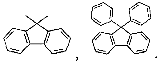
- In the present invention, an example of the aryl amine group means substituted or unsubstituted monocyclic diarylamine group, substituted or unsubstituted polycyclic diarylamine group or substituted or unsubstituted monocyclic and polycyclic diarylamine group.
- In the present invention, the term "substituted or unsubstituted" means that it is substituted or unsubstituted by at least one substituent group of heavy hydrogen; halogen group; nitrile group; nitro group; hydroxy group; cycloalkyl group; alkoxy group; aryloxy group; alkylthioxy group; arylthioxy group; alkylsulfoxy group; arylsulfoxy group; alkenyl group; silyl group; boron group; alkylamine group; aralykylamine group; arylamine group; aryl group; fluorenyl group; carbazole group; and the heteroring group that includes one or more of N, O, and S atoms.
- In the compound according to the present invention, in the case of when p of -(L)p-(Y)q is 0, it is preferable that at least one of Y is heavy hydrogen, nitrile group, halogen group, substituted or unsubstituted boron group, substituted or unsubstituted aryl group, substituted or unsubstituted heteroring group.
- In the compound according to the present invention, in the case of when p of -(L)p-(Y)q is 1 or more, it is preferable that L is substituted or unsubstituted arylene group, or substituted or unsubstituted heteroarylene group, and it is preferable that Y is substituted or unsubstituted boron group; substituted or unsubstituted alkylamine group; substituted or unsubstituted aralykylamine group; substituted or unsubstituted arylamine group; substituted or unsubstituted heteroarylamine group; substituted or unsubstituted aryl group; substituted or unsubstituted fluorenyl group; substituted or unsubstituted carbazole group; or substituted or unsubstituted heteroring group that includes one or more of n, o, and s atoms.
- In Formula 3-1 or 4-1, in the case of when L is an arylene group or heteroallylene group, and Y is an aryl group or heteroaryl group, it is preferable that p + q is 2 or more.
- In the case of when p of -(L)p-(Y)q is 2 or more, L is the same as or different from each other, and in the case of when q of -(L)p-(Y)q is 2 or more, Y is the same as or different from each other.
- In the compound according to the present invention, it is preferable that at least one of R3 to R12 is heavy hydrogen, nitrile group, halogen group, aryl group, substituted arylene group, heteroring group, substituted heteroring group, fluorenyl group, carbazole group.
- In the present invention, the substituted arylene group means that phenyl group, biphenyl group, naphthalene group, fluorenyl group, pyrenyl group, phenanthrenyl group, perylene group, tetracenyl group, anthracenyl group are substituted by the other substituent group.
- In the present invention, the substituted heteroarylene group means a group in which pyridyl group, thiophenyl group, triazine group, quinoline group, phenanthroline group, imidazole group, thiazole group, oxazole group, carbazole group and condensate heteroring group thereof, for example, benzquinoline group, benzimidazole group, benzoxazole group, benzthiazole group, benzcarbazole group, dibenzothiophenyl group are substituted.
- In Formulas 3-1, and 4-1, (N)n1 and (N)n2 means that the carbon atom in the ring is capable of being substituted by the nitrogen atom. Herein, it is preferable that n1 and n2 are each independently an integer in the range of 0 to 2.
- The vacuum deposition process of the manufacturing method of the organic light emitting device performs deposition by subliming a material at the high vacuum, for example, about 10-6 to 10-7 torr and high temperature. Accordingly, it is important to maintain the property of the compound at a high temperature for a long time without deformation and easily sublime it.
- Meanwhile, the imidazole group is a heteroring compound that includes two nitrogen atoms in the pentagonal ring, and has excellent electron injection and electron transport properties, such that it is used as the electron injection and electron transport layer or the light emitting layer in the organic light emitting device. The compound TPBi that is Formula X-1 and Formula X-2 has an ability for functionally transporting electrons and an ability for blocking holes flowing to the light emitting layer, such that it is capable of being used as a hole blocking layer. However, it has a problem in that stability is too low to apply it to a real device. Therefore, in the present invention, even though it has excellent characteristic performance, the problem thereof of physically or electrically low stability will be overcome.
- In order to maintain the properties of the compound without a deformation in the organic light emitting device, the compound should be electrically stable, and high glass transition temperature (Tg) and high melting point (Tm) in physical view. However, Formula X-1 and Formula X-2 have very low Tg and Tm.
- In addition, in the course of manufacturing the organic light emitting device, since the compounds are deposited under the vacuum for a long time at high temperature, the compounds that have low thermal stability are easily deformed, such that it cannot be deposited under the vacuum for a long time. In order to overcome this, the material that is capable of being sublimed at a low temperature and a high subliming ability is required. In order to have the high subliming ability at the low temperature, the molecular weight of the compound should be lowered or interaction between the molecules should be lowered. In addition, the crystallinity is increased by deforming the structure of the compound, such that the subliming ability is increased at Tg or Tm or less, and it is preferable that the structure of the compound is a plate structure, a symmetric structure, or a spherical structure.
- In the present invention, it is deemed that the reduction in stability of the N-phenylbenzimidazole group may be caused by free rotation of N and the phenyl group like the following structure, and if 2-position and N-phenyl group obtain heat energy by the free rotation, it may be activated, such that the reduction in stability of the compound may be caused.
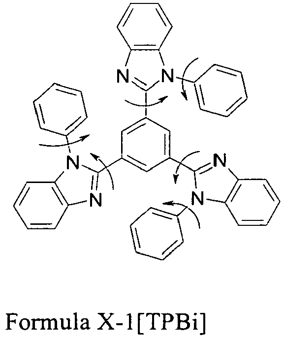

- In order to overcome the problems, the present invention, as shown in Formula 3-1 or 4-1 connects the ortho position of the aryl group or heteroaryl group that includes X1 to X4 bonded to
N of the imidazole group, and the ortho position of the aryl group or heteroaryl group that includes Y1 to Y4 bonded to the 2-position of the imidazole group to each other to increase the stability and the subliming ability of the compound. - The structure of the compound of Formula 3-1 or 4-1 that is developed as described above approaches the plate structure,
such that the thermal stability and the subliming ability are more increased. The structure of Formula 3-1 or 4-1 makes the free rotation difficult and increases the thermal stability and the subliming ability, such that the stability can be maintained in the vacuum deposition process. - In the case of when the substituent group of Formula 3-1 or 4-1 is aryl group or heteroaryl
group, it is most preferable in views of stability, and the substituent having the large rotation like the alkyl group is less preferable. - In addition, in the case of the compound in which the halogen, nitrile group, nitro group, or heteroring group is introduced to the above Formula, the HOMO value of the compound is made deep, such that the hole flowing from the light emitting layer can be blocked and the amount of hole remaining in the light emitting layer is increased, thereby increasing efficiency and stability.
- In addition, the compound according to the present invention may be used for various purposes in the organic light emitting electronic device according to the kind and the property of the substituent group. For example, in the case of when the substituted or unsubstituted aryl group or heteroaryl group is substituted, or two or more structures of Formula 1 are connected to each other, since the properties thereof have a deep HOMO value and an appropriate LUMO value that is capable of injecting electrons well because of an increase in electron affinity and electronegativity, it is advantageous that it is used as the electron injection, electron transport or hole blocking layer. Meanwhile, since the substituted or unsubstituted arylamino group, alkylamino group, heteroarylamino group, arylkylamino group and aryl group or heteroaryl group that is substituted by them relatively well form the holes, it is useful to hole injection and transport layer. Basically, since the structure of Formula 3-1 or 4-1 has very large band gap, if the substituent that is suitable to the strure of Formula 3-1 or 4-1 is introduced, for example if the substituent such as carbazole group is introduced, the energy bandgap and stability in a triplet state can be ensured. From these results, various phosphorescence dopants from red color to blue color can be used and applied to light emitting layers of fluorescent and phosphorescent devices. In particular, the compound according to the present invention may be used as the host of the light emitting layer. In the case of when the compound according to the present invention is used as the host of any one organic material layer of the organic light emitting device, for example, the light emitting layer or the electron transport layer, the other organic compounds, metal or metal compounds may be used as the dopant.
- As preferable detailed examples of the compound that is represented by Formula 3-1 or 4-1 there are the following compounds, but they are not limited thereto.


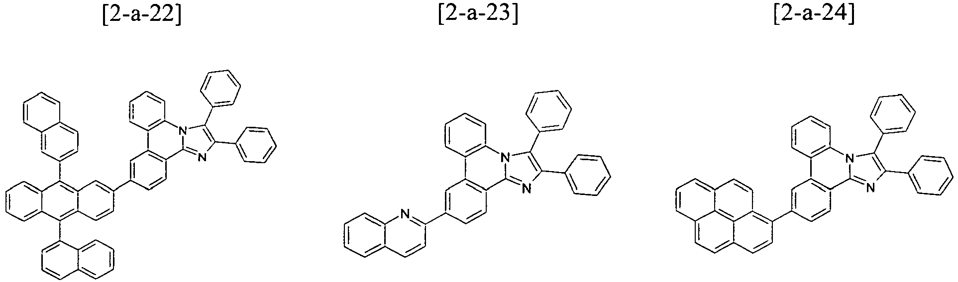



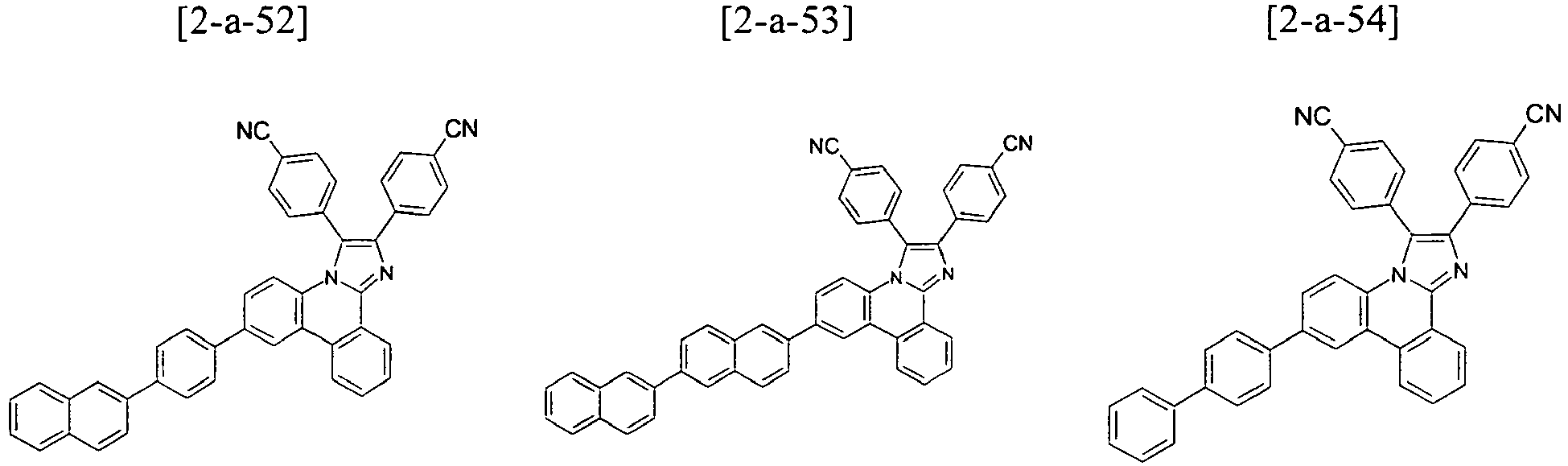

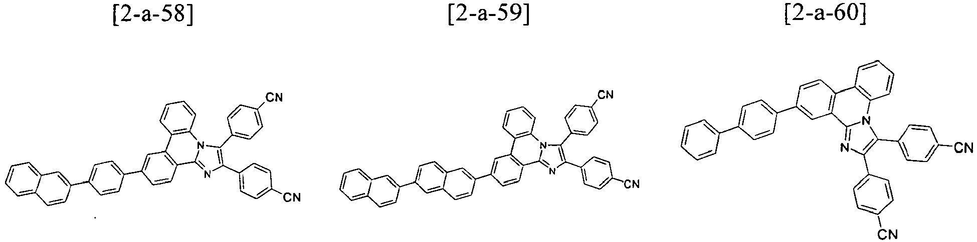


- As preferable detailed examples of the compound that is represented by Formula 3-1 or 4-1 there are the following compounds, but they are not limited thereto.





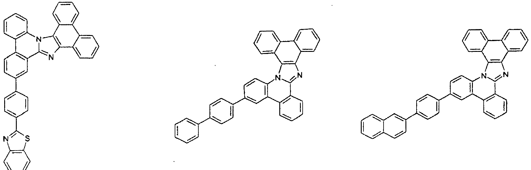


- In addition, the present invention provides a method for manufacturing the derivative that is represented by Formula 3-1 or 4-1.
- The compound (Cpd C) that is represented by Formula 3-1 or 4-1 may be prepared by using the following method. First, under the Pd catalyst, after the compound Cpd A is prepared through a Suzuki bonding reaction, the imidazole derivative Cpd B may be prepared by reacting the compound to which 1,2-diaminobenzene and the formyl group are introduced. Next, the structure of Formula 3-1 or 4-1 may be manufactured through the cyclization reaction of the -NH of the imidazole group and the aryl group or heteroaryl group that includes the chloro (Cl) group in the molecule under the Pd catalyst. As described above, Formula 3-1 or 4-1 in which the ortho position of the aryl group or heteroaryl group that includes X1 to X4 and the ortho position of the aryl group or heteroaryl group that includes Y1 to Y4 are connected to each other may be prepared.
- In detail, the compound that is represented by Cpd B
may be prepared through 1) the Suzuki bonding reaction of the compound Cpd 1 in which halogens are substituted,boronic acid Cpd 2 in which the formyl group is substituted, orboron ester Cpd 3 under the Pd catalyst. Also, it may be prepared through the Suzuki bonding reaction of boronic acid Cpd 4 in which halogens are substituted,boron ester Cpd 5, or thecompound Cpd 6 in which the formyl group is substituted under the Pd catalyst. - The manufacturing method may be represented by the following Reaction Equation 1.


- In detail, the compound that is represented by Cpd A
may prepare 2) the imidazole group through the acid catalyst by mixing Cpd A in which the halogen group and the formyl group are substituted, the diketo derivative (Cpd 7) that has the R1 and R2 substituents, and, ammonium acetate. Also, it may prepare the imidazole group through the acid catalyst by mixing Cpd A in which the halogen group and the formyl group are substituted, the diamine derivative (Cpd 8) that has the R1 and R2 substituents. - The manufacturing method may be represented by the following
Reaction Equation 2.

- In detail, the compound that is represented by Cpd C
may prepared Cpd C (Formula 1) through 3) the cyclization reaction of the halogen group and Cpd B in which the imidazole group is substituted by using the Pd catalyst in the molecule. - The manufacturing method may be represented by the following
Reaction Equation 3.
- Additionally, by introducing various substituent groups into the core structure, compounds having intrinsic characteristics of the substituent groups may be obtained. For example, substituent groups, which are frequently applied to hole injection layer material, hole transport layer material, light emitting layer material, and electron transport layer materials during the production of the organic light emitting device and the organic electronic device, are introduced into the core structure so as to produce substances capable of satisfying the requirements of each organic material layer.
- In Formula 3-1 or 4-1 in the case of when Y is the aryl group, the aryl group has stability in respects to both electrons and holes, and in particular, in the case of when L has a predetermined length, it is possible to control the bandgap. In addition, it is possible to ensure thermal stability, the subliming ability, and electric stability, and in the real device, it is possible to improve performance.


- In Formula 1, in the case of when p of -(L)p- is 0 and the core structure is directly connected to Y, stability is shown in respects to the electrons and the holes in terms of the properties of the substituent group, and an appropriate Tg (glass transition temperature) is ensured, thereby improving thermal stability.
- In the compound in which

- In addition, if an appropriate substituent, for example, carbazole or benzcarbazole, is introduced to the structure of Formula 3-1 or 4-1, energy band gap (e.g. FIG. 30) and stability can be ensured at a triplet state. From these results, various phosphorescence dopants from red color to blue color can be used and applied to the host of the light emitting layers of fluorescent and phosphorescent devices.
As a result, since the structure of Formula 3-1 or 4-1 including the appropriate substituent has a high glass transition temperature (Tg), it has excellent thermal stability. Such increase in thermal stability is an important factor providing driving stability to the device. According to the length and the kind of the substituent group, it is possible to finely control HOMO and LUMO energy level and energy band gap, improve interfacial characteristics with organic materials, and make the purpose of material various. - Since the compound according to the present invention is freely controlled by the core and the substituent, it may act as various layers in addition to the host of the phosphorescent or fluorescent light emitting layer.
- In addition, the present invention provides an organic electronic device which includes a first electrode, a second electrode, and one or more organic material layers that are disposed between the first electrode and the second electrode, wherein one or more layers of the organic material layers include the compound that is represented by Formula 3-1 or 4-1.
- The organic electronic device is selected from the group consisting of an organic light emitting device, an organic solar cell, an organic photoconductor (OPC) drum and an organic transistor.
- In addition, the organic electronic device may be an organic light emitting device.
- In addition, the organic light emitting device may be an organic light emitting device that has a positive direction structure, in which an anode, one or more organic material layers and a cathode are sequentially layered on a substrate.
- In addition, the organic light emitting device may be an organic light emitting device that has a negative direction structure, in which a cathode, one or more organic material layers and an anode are sequentially layered on a substrate.
- In addition, the organic material layer of the organic light emitting device may include a hole injection layer, a hole transport layer, a light emitting layer, and an electron injection and/or transport layer.
- In addition, the organic material layer of the organic light emitting device includes a light emitting layer, and the light emitting layer includes the nitrogen-containing heterocyclic derivative. At this time, the nitrogen-containing heterocyclic derivative may act as a host of the light emitting layer.
- In addition, the organic material layer of the organic light emitting device includes an electron transport and/or injection layer, and the layer includes the nitrogen-containing heterocyclic derivative.
- In addition, the organic material layer of the organic light emitting device includes a layer that simultaneously transport holes and emit light, and the layer includes the nitrogen-containing heterocyclic derivative.
- In addition, the organic material layer of the organic light emitting device includes a layer that simultaneously transport electrons and emit light, and the layer includes the nitrogen-containing heterocyclic derivative.
- The organic material layer that includes the nitrogen-containing heterocyclic derivative according to the present invention includes the nitrogen-containing heterocyclic derivative as the host, and other organic compounds, metal or metal compounds as a dopant.
- It is preferable that the organic electronic device according to the present invention includes the organic material layer including the nitrogen-containing heterocyclic derivative, and a hole injection layer or a hole transport layer that includes the compound including arylamino group, carbazole group or benzcarbazole group.
- The organic electronic device according to the present invention may be manufactured by using a manufacturing method and a material of a general organic electronic device, except that one or more organic material layers are formed by using the above compounds.
- Hereinafter, the organic light emitting device will be described.
- In an embodiment of the present invention, the organic light emitting device may be comprised of a first electrode, a second electrode and an organic material layer that is disposed between them. The organic material layer of the organic light emitting device according to the present invention may have a single layer structure including one layer and a multilayered structure that includes two or more layers including a light emitting layer. In the case of when the organic material layer of the organic light emitting device according to the present invention has the multilayered structure, for example, this may be a structure in which hole injection layer, hole transport layer, light emitting layer, electron transport layer and the like are layered. However, the structure of the organic light emitting device is not limited to this, but may comprise a smaller number of organic material layers. For example, the organic light emitting device according to the present invention may have the same structure as the structure shown in
FIG. 1 . InFIG. 1 , reference numeral 1 means a substrate,reference numeral 2 means an anode,reference numeral 3 means a hole injection layer, reference numeral 4 means a hole transport layer,reference numeral 5 means an organic light emitting layer,reference numeral 6 means an electronic transport layer,reference numeral 7 means a cathode. The organic light emitting device that has the same structure asFIG. 1 is an organic light emitting device having a positive direction structure, but the present invention is not limited thereto but includes an organic light emitting device having a negative direction structure. That is, the organic light emitting device according to the present invention may have a structure in which a substrate, a cathode, an electronic transport layer, an organic light emitting layer, a hole transport layer, a hole injection layer, and an anode are sequentially layered. - In the case of when the organic light emitting device according to the present invention has the organic material layer having a multilayered structure, the compound of Formula 1 may be included in a light emitting layer, a hole transport layer, a layer that performs simultaneously hole transport and light emission, a layer that performs simultaneously electron transport and light emission, an electronic transport layer, and an electron transport and/or injection layer. In the present invention, it is preferably that the compound of Formula 3-1 or 4-1 is included in the electron injection and/or transport or light emitting layer.
- The organic light emitting device according to the present invention may be manufactured by using the general manufacturing method and the material of the organic light emitting device, except that the compound of Formula 3-1 or 4-1 is used in one or more of the organic material layers of the organic light emitting device. For example, the organic light emitting device according to the present invention may be manufactured by forming an anode by depositing metal or metal oxides having the conductivity or an alloy thereof on a substrate by using a PVD(physical vapor deposition) method such as sputtering or e-beam evaporation, forming the organic material layer that includes hole injection layer, hole transport layer, light emitting layer and electron transport layer thereon, and depositing the material that is capable of being used as a cathode thereon. In addition to this method, in order to manufacture the organic light emitting device having the negative direction structure, an organic light emitting device may be manufactured by sequentially depositing a cathode, an organic material layer, and an anode material on a substrate.
- The organic material layer may be manufactured in a smaller number of layer by using various polymer materials and by using not a deposition method but a solvent process, for example, spin coating, dip coating, doctor blading, screen printing, inkjet printing, heat transferring method and the like.
- As the anode material, in general, it is preferable to use the material having the large work function so as to smoothly perform hole injection into the organic material layer. As examples of the anode material that is capable of being used in the present invention, there are metal or alloy thereof such as vanadium, chrome, copper, zinc, gold and the like; metal oxides such as zinc oxides, indium oxides, indium tin oxides (ITO), indium zinc oxides (IZO) and the like; a combination of metal and oxides such as ZnO:Al or SnO2:Sb; conductive polymers such as poly(3-methyl compound), poly[3,4-(ethylene-1,2-dioxy) compound](PEDOT), polypyrole and polyaniline, but it is not limited thereto.
- As the cathode material, in general, it is preferable to use the material having the small work function so as to smoothly perform electron injection into the organic material layer. As detailed examples of the cathode material, there are metal such as magnesium, calcium, sodium, potassium, titanium, indium, yttrium, lithium, gadolinium, aluminum, silver, tin, and lead or an alloy thereof; a multilayered structure material such as LiF/Al or LiO2/Al, but it is not limited thereto.
- The hole injection material is a material that is capable of well receiving holes from the anode at a low voltage, and it is preferable that the HOMO (highest occupied molecular orbital) of the hole injection material is a value between the work function of the anode material and the HOMO of the organic material layer around them. As detailed examples of the hole injection material, there are metal porphyrine, oligo thiophene, arylamine-based organic material, hexanitrilehexaazatriphenylene-based organic material, quinacridone-based organic material, perylene-based organic material, anthraquinone and polyaniline and poly thiophene-based conductive polymers, but it is not limited thereto.
- The hole transport material is a material that receives the holes from the anode or the hole injection layer and transfer them to the light emitting layer, and it is preferable to use the material having the large mobility to the holes. As detailed examples thereof, there are arylamine-based compound, carbazole-based compound, anthracene-based compound, pyrene-based compound, a conductive polymer, and a block copolymer in which a conjugate portion and a conjugate portion are simultaneously included, but it is not limited thereto.
- The light emitting material is a material that receives the holes and the electrons from the hole transport layer and the electron transport layer, combines them, such that light at a range of visible rays is emitted, and it is preferable to use the material having excellent photon efficiency to fluorescence or phosphorescence. As detailed examples thereof, there are a 8-hydroxy-quinoline aluminium complex (Alq3); a carbazole-based compound; a dimerized styryl compound; bis-methyl-8-hydroxyquinoline paraphenylphenol aluminum complex (Balq); 10-hydroxybenzoquinoline-metal compound; a benzoxazole, benzthiazole and benzimidazole-based compound; an anthracene-based compound; a pyrene-based compound; a poly(p-phenylenevinylene) (PPV)-based polymer; a spiro compound; polyfluorene, lubrene, and the like, but it is not limited thereto.
- The electron transport material is a material that receives the electrons from the cathode and transfer them to the light emitting layer, and it is preferable to use the material having the large mobility to the electrons. As detailed examples thereof, there are A1 complex of 8-hydroxyquinoline; complex including Alq3; organic radical compounds; hydroxyflavone-metal complexes; anthracene-based compounds; pyrene-based compounds; benzoxazole, benzthiazole and benzimidazole-based compounds; pyridyl-based compounds; penanthroline-based compounds; quinoline-based compounds; quinazoline-based compounds and the like, and these compounds may be doped with metal or metal compounds to form the electron transport layer, but they are not limited thereto.
- The organic light emitting device according to the present invention may be a front side light emitting type, a rear side light emitting type, or a both sides light emitting type according to the used material.
- The compound according to the present invention may be operated in a principle that is similar to a principle applied to the organic light emitting device in organic solar cell, organic photoconductor, organic transistor, and organic electronic device. Hereinafter, preferable Examples will be described in order to help understanding of the present invention. The following Examples are set forth to illustrate but are not to be construed to limit the present invention.
-

- After 1-bromo-2,5-dichlorobenzene (15.6 g, 69.1 mmol) and 2-formylphenylboronic acid (11.4 g, 76 mmol) were dissolved in tetrahydrofuran (THF) (200 mL), 2M potassium carbonate aqueous solution (70 mL) was added thereto, and tetrakistriphenylphosphino palladium (Pd(PPh3)4 (1.6 g, 2 mol%) was put thereinto, agitated and refluxed for 5 hours. The temperature was lowered to normal temperature, the water layer was removed, and the organic layer was dried with anhydrous magnesium sulfate (MgSO4) and filtered. The filtered solution was concentrated under the reduced pressure, and columned with tetrahydrofuran:hexane = 1:10 to prepare the compound A-1 (13.9 g, 80%). MS:[M+H]+=251
- The compound A-1(17.3 g, 69.1 mmol) that was prepared in Preparation Example 1 and diaminobenzene (7.47 g, 69.1 mmol) were suspended in dioxane (1,4-dioxane) (200 mL) and the acetic acid (AcOH) (20 mL). The mixture was agitated and refluxed for about 6 hours, and cooled to normal temperature. After the mixture was diluted with water (100 mL), the generated solid was filtered, washed with water and ethyl ether to prepare the compound A-2 (12.9 g, 55%). MS:[M+H]+=339
- The compound A-2 (1.7 g, 5.1 mmol) that was prepared in Preparation Example 2 and sodium-tertiary-butoxide (NaOt-Bu) (0.58 g, 6.01 mmol) and Pd[P(t-Bu)3]2 (51 mg, 2 mol%) were suspended in toluene (50 mL). The mixture was agitated and refluxed for about 6 hours, and cooled to normal temperature. Distilled water was put into the reaction solution, the termination of the reaction was carried out, and the organic material layer was extracted and dried with anhydrous magnesium sulfate (MgSO4) and filtered. The filtered solution was concentrated under the reduced pressure, and columned with tetrahydrofuran:hexane = 1:5 to prepare the compound A-3 (0.618 g, 40%). MS: [M+H]+=303
- The compound A-3 (5.1 g, 16.8 mmol) that was prepared in Preparation Example 3, bis(pinacolato) diboron (4.7 g, 18.5 mmol) and potassium acetate (4.96 g, 50.5 mmol) were suspended in dioxane (100 mL). To the suspension solution, Pd(dba)2 (0.29 g, 3 mol%) and PCy3 (0.28 g, 6 mol%) were added. The mixture was agitated and refluxed for about 8 hours, and cooled to normal temperature. The mixture was diluted with water (100 mL), and extracted with dichloromethane (3 × 50 mL). The organic extract material was dried over magnesium sulfate and filtered. The filtered solution was concentrated under the reduced pressure, recrystallized with ethyl ether and hexane to prepare the compound A-4 (5.62 g, 85%). MS:[M+H]+=395
-

- The compound A-2 (2.51 g, 10 mmol) that was prepared in Preparation Example 2, Benzil (2.1 g, 10 mmol), and ammonium acetate (2.32 g, 30 mmol) were suspended in the acetic acid (20 mL). The mixture was agitated and refluxed for about 6 hours, and cooled to normal temperature. After the mixture was diluted with water (50 mL), the generated solid was filtered, washed with water and ethyl ether to prepare the compound (2.73 g, 62%). MS:[M+H]+=441
- The compound A-6 (0.929 g, 45%) was prepared by using the same method as Preparation Example 3, except that the compound A-5 that was prepared in Preparation Example 5 was used instead of the compound A-2 in Preparation Example 3. MS:[M+H]+=405
- The compound A-7 (6.85 g, 82%) was prepared by using the same method as Preparation Example 4, except that the compound A-6 that was prepared in Preparation Example 6 was used instead of the compound A-3 in Preparation Example 4. MS:[M+H]+=497
-

- The compound A-2 (2.51 g, 10 mmol) that was prepared in Preparation Example 2, 9,10-Phenanthrenequinone (2.08 g, 10 mmol) and ammonium acetate (2.32 g, 30 mmol) were suspended in the acetic acid (20 mL). The mixture was agitated and refluxed for about 6 hours, and cooled to normal temperature. After the mixture was diluted with water (50 mL), the generated solid was filtered, washed with water and ethyl ether to prepare the compound A-8 (3.07 g, 70%). MS: [M+H]+=439
- The compound A-9 (0.863 g, 42%) was prepared by using the same method as Preparation Example 3, except that the compound A-8 that was prepared in Preparation Example 8 was used instead of the compound A-2 in Preparation Example 3. MS:[M+H]+=403
- The compound A-10 (6.24 g, 75%) was prepared by using the same method as Preparation Example 4, except that the compound A-9 that was prepared in Preparation Example 9 was used instead of the compound A-3 in Preparation Example 4. MS:[M+H]+=495
-

- After 2-bromo-4-chlorobenzaldehyde (15.1 g, 69.1 mmol) and 2-chlorophenylboronic acid (11.9 g, 76 mmol) were dissolved in tetrahydrofuran (THF) (200 mL), 2M potassium carbonate aqueous solution (70 mL) was added thereto, and tetrakistriphenylphosphino palladium (Pd(PPh3)4(1.6 g, 2 mol%) was put thereinto, agitated and refluxed for 5 hours. The temperature was lowered to normal temperature, the water layer was removed, and the organic layer was dried with anhydrous magnesium sulfate and filtered. The filtered solution was concentrated under the reduced pressure, and columned with tetrahydrofuran:hexane = 1:10 to prepare the compound A-11 (13.0 g, 80%). MS: [M+H]+=251
- The compound A-11(17.3 g, 69.1 mmol) that was prepared in Preparation Example 11 and diaminobenzene (7.47 g, 69.1 mmol) were suspended in dioxane (1,4-dioxane) (200 mL) and the acetic acid (AcOH) (20 mL). The mixture was agitated and refluxed for about 6 hours, and cooled to normal temperature. After the mixture was diluted with water (100 mL), the generated solid was filtered, washed with water and ethyl ether to prepare the compound A-12 (13.4g, 57%). MS:[M+H]+=339
- The compound A-12 (1.7 g, 5.1 mmol) that was prepared in Preparation Example 12 and sodium-tertiary-butoxide (NaOt-Bu) (0.58 g, 6.01 mmol) and Pd[P(t-Bu)3]12 (51 mg, 2 mol%) were suspended in toluene (50 mL). The mixture was agitated and refluxed for about 6 hours, and cooled to normal temperature. Distilled water was put into the reaction solution, the termination of the reaction was carried out, and the organic material layer was extracted and dried with anhydrous magnesium sulfate (MgSO4) and filtered. The filtered solution was concentrated under the reduced pressure, and columned with tetrahydrofuran:hexane = 1:5 to prepare the compound A-13 (0.664 g, 43%). MS: [M+H]+=303
- The compound A-13 (5.1 g, 16.8 mmol) that was prepared in Preparation Example 13, bis(pinacolato) diboron (4.7 g, 18.5 mmol) and potassium acetate (4.96 g, 50.5 mmol) were suspended in dioxane (100 mL). To the suspension solution, Pd(dba)2 (0.29 g, 3 mol%) and PCy3 (0.28 g, 6 mol%) were added. The mixture was agitated and refluxed for about 8 hours, and cooled to normal temperature. The mixture was diluted with water (100 mL), and extracted with dichloromethane (3 × 50 mL). The organic extract material was dried over magnesium sulfate and filtered. The filtered solution was concentrated under the reduced pressure, recrystallized with ethyl ether and hexane to prepare the compound A-14 (5.95 g, 90%). MS:[M+H]+=395
-

- The compound A-12 (2.51 g, 10 mmol) that was prepared in Preparation Example 12, benzil (2.1 g, 10 mmol) and ammonium acetate (2.32 g, 30 mmol) were suspended in the acetic acid (20 mL). The mixture was agitated and refluxed for about 6 hours, and cooled to normal temperature. After the mixture was diluted with water (50 mL), the generated solid was filtered, washed with water and ethyl ether to prepare the compound A-15 (3.09 g, 70%). MS: [M+H]+=441
- The compound A-16 (0.847 g, 41%) was prepared by using the same method as Preparation Example 13, except that the compound A-15 that was prepared in Preparation Example 15 was used instead of the compound A-12 in Preparation Example 13. MS:[M+H]+=405
- The compound A-17 (7.09 g, 85%) was prepared by using the same method as Preparation Example 14, except that the compound A-16 that was prepared in Preparation Example 16 was used instead of the compound A-13 in Preparation Example 14. MS:[M+H]+=497
-
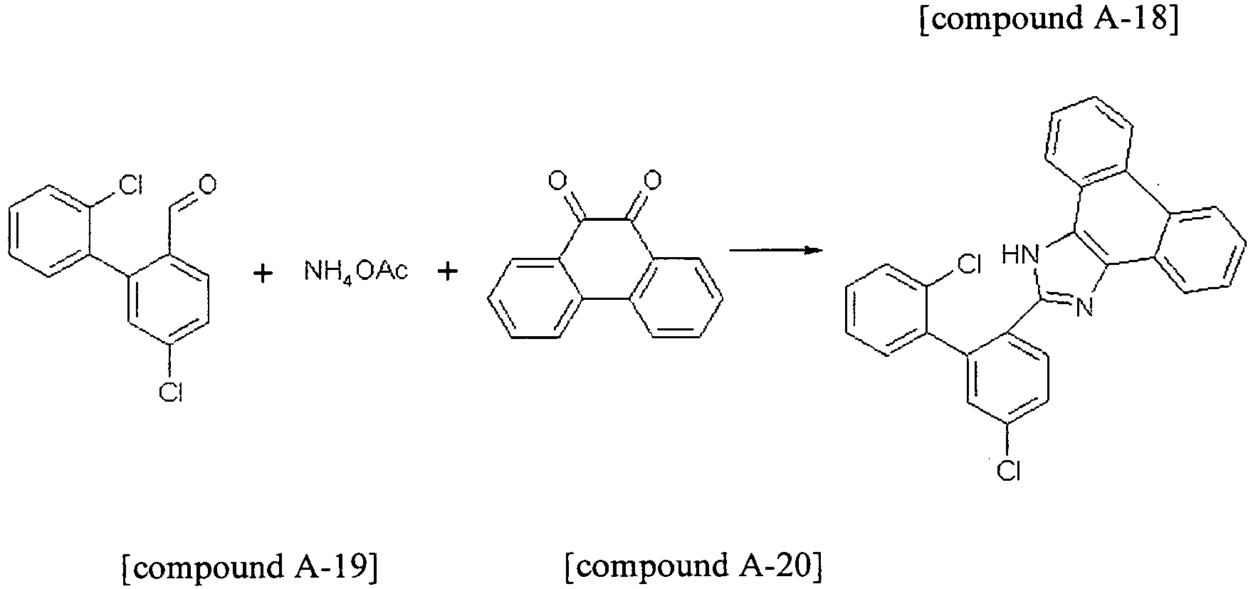

- The compound A-12 (2.51 g, 10 mmol) that was prepared in Preparation Example 12, 9,10-Phenanthrenequinone (2.08 g, 10 mmol) and ammonium acetate (2.32 g, 30 mmol) were suspended in the acetic acid (20 mL). The mixture was agitated and refluxed for about 6 hours, and cooled to normal temperature. After the mixture was diluted with water (50 mL), the generated solid was filtered, washed with water and ethyl ether to prepare the compound A-18 (3.51 g, 80 %). MS: [M+H]+=439
- The compound A-19 (0.822 g, 40%) was prepared by using the same method as Preparation Example 13, except that the compound A-18 that was prepared in Preparation Example 18 was used instead of the compound A-12 in Preparation Example 13. MS:[M+H]+=403
- The compound A-20 (6.82 g, 82%) was prepared by using the same method as Preparation Example 14, except that the compound A-19 that was prepared in Preparation Example 19 was used instead of the compound A-13 in Preparation Example 14. MS:[M+H]+=495
-

- After 2-chloro-bromobenzene (13.2 g, 69.1 mmol) and 2-formylphenylboronic acid (11.4 g, 76 mmol) were dissolved in tetrahydrofuran (THF) (200 mL), 2M potassium carbonate aqueous solution (70 mL) was added thereto, and tetrakistriphenylphosphino palladium (Pd(PPh3)4 (1.6 g, 2 mol%) was put thereinto, agitated and refluxed for 5 hours. The temperature was lowered to normal temperature, the water layer was removed, and the organic layer was dried with anhydrous magnesium sulfate and filtered. The filtered solution was concentrated under the reduced pressure, and columned with tetrahydrofuran:hexane=1:10 to prepare the compound A-21 (11.2 g, 75 %). MS:[M+H]+=217
- The compound A-21 (14.9 g, 69.1 mmol) that was prepared in Preparation Example 21 and 2-azido-5-chlorobenzeneamine (11.6 g, 69.1 mmol) were suspended in ethanol (200 mL) and the acetic acid (10 mL). The mixture was agitated and refluxed for about 21 hours. The temperature was lowered to normal temperature, concentrated under the reduced pressure, and recrystallized with hexane to prepare the compound A-22 (5.85 g, 25%). MS: [M+H]+=339
- The compound A-22 (1.73 g, 5.1 mmol) that was prepared in Preparation Example 22 and sodium-tertiary-butoxide (NaOt-Bu) (0.58 g, 6.01 mmol) and Pd[P(t-Bu)3]22 (51 mg, 2 mol%) were suspended in toluene (50 mL). The mixture was agitated and refluxed for about 6 hours, and cooled to normal temperature. Distilled water was put into the reaction solution, the termination of the reaction was carried out, and the organic material layer was extracted and dried with anhydrous magnesium sulfate and filtered. The filtered solution was concentrated under the reduced pressure, and columned with tetrahydrofuran:hexane=1:5 to prepare the compound A-23 (0.618 g, 40%). MS: [M+H]+=303
- The compound A-23 (5.09 g, 16.8 mmol) that was prepared in Preparation Example 23, bis(pinacolato) diboron (4.7 g, 18.5 mmol) and potassium acetate (4.96 g, 50.5 mmol) were suspended in dioxane (100 mL). To the suspension solution, Pd(dba)2 (0.29 g, 3 mol%) and PCy3 (0.28 g, 6 mol%) were added. The mixture was agitated and refluxed for about 8 hours, and cooled to normal temperature. The mixture was diluted with water (100 mL), and extracted with dichloromethane (3 × 50 mL). The organic extract material was dried over magnesium sulfate and filtered. The filtered solution was concentrated under the reduced pressure, recrystallized with ethyl ether and hexane to prepare the compound A-24 (5.3 g, 80%). MS:[M+H]+=395
-

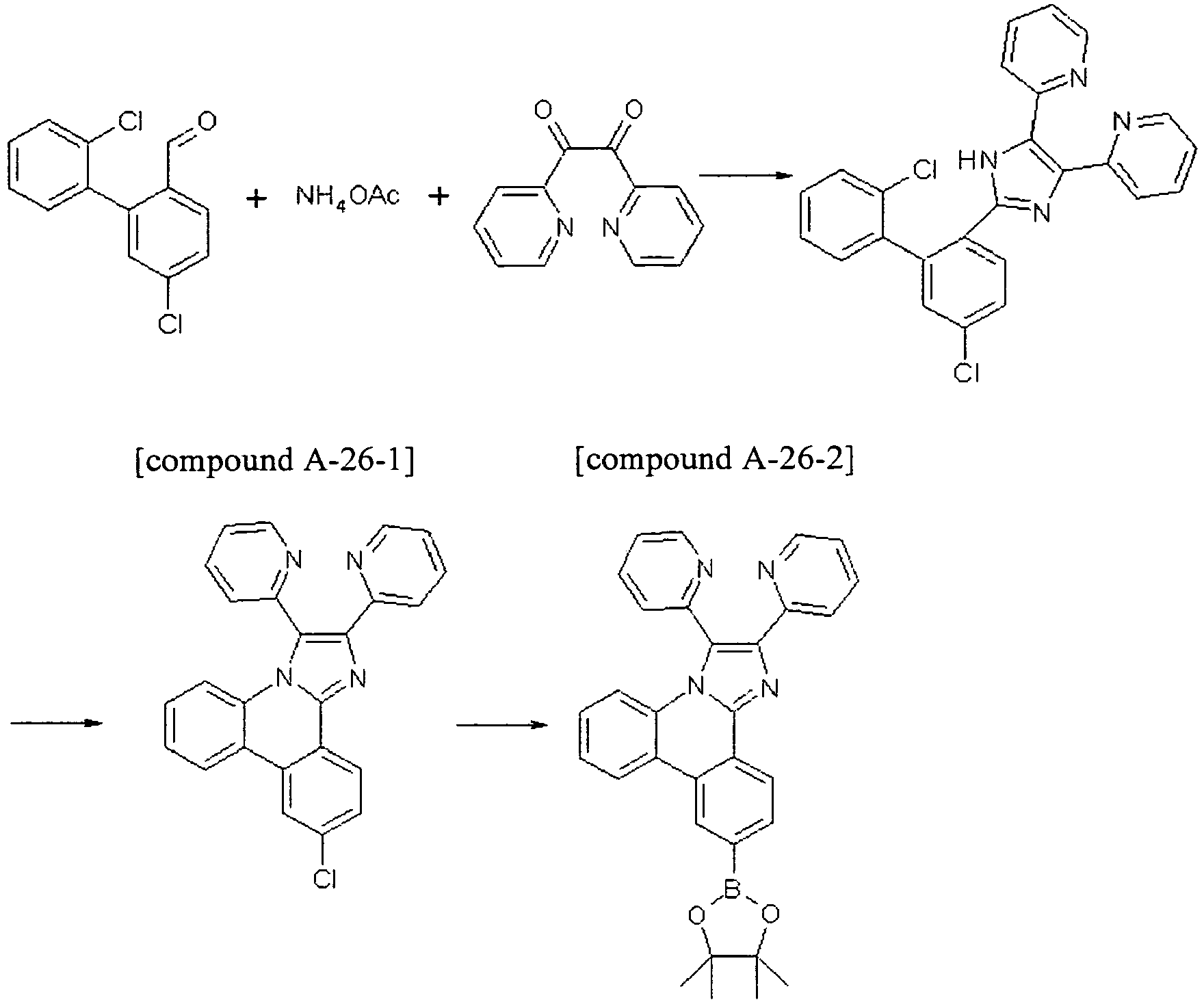
- The compound A-11 (2.51 g, 10 mmol) that was prepared in Preparation Example 11, 2,2'-Pyridil (2.12 g, 10 mmol) and ammonium acetate (2.32 g, 30 mmol) were suspended in the acetic acid (20 mL). The mixture was agitated and refluxed for about 6 hours, and cooled to normal temperature. After the mixture was diluted with water (50 mL), the generated solid was filtered, washed with water and ethyl ether to prepare the compound A-25 (2.66 g, 60 %).
MS: [M+H]+=443 - The compound A-26-1 (0.726 g, 35%) was prepared by using the same method as Preparation Example 13, except that the compound A-25 that was prepared in Preparation Example 25 was used instead of the compound A-12 in Preparation Example 13. MS:[M+H]+=407
- The compound A-26-2 (3.35 g, 40%) was prepared by using the same method as Preparation Example 14, except that the compound A-26-1 that was prepared as described above was used instead of the compound A-13 in Preparation Example 14. MS:[M+H]+=499
-

- After 2-bromo-3-chloro-pyridine (13.26 g, 69.1 mmol) and 5-chloro-2-formyl-benzeneboronic acid (13.98 g, 76 mmol) were dissolved in tetrahydrofuran (THF) (200 mL), 2M potassium carbonate aqueous solution (70 mL) was added thereto, and tetrakistriphenylphosphino palladium (Pd(PPh3)4) (1.6 g, 2 mol%) was put thereinto, agitated and refluxed for 5 hours. The temperature was lowered to normal temperature, the water layer was removed, and the organic layer was dried with anhydrous magnesium sulfate and filtered. The filtered solution was concentrated under the reduced pressure, recrystallized with hexane to prepare the compound A-27 (7 g, 40 %). MS: [M+H]+=252
- The compound A-28 (9.4 g, 40%) was prepared by using the same method as Preparation Example 12, except that the compound A-27 that was prepared in Preparation Example 27 was used instead of the compound A-11 in Preparation Example 12. MS: [M+H]+=340
- The compound A-29 (0.620 g, 40%) was prepared by using the same method as Preparation Example 13, except that the compound A-28 that was prepared in Preparation Example 28 was used instead of the compound A-12 in Preparation Example 13. MS:[M+H]+=304
- The compound A-30 (4.32 g, 65%) was prepared by using the same method as Preparation Example 14, except that the compound A-29 that was prepared in Preparation Example 29 was used instead of the compound A-13 in Preparation Example 14. MS:[M+H]+=396
-


- After 2-bromo-3-formyl-pyridine (12.85 g, 69.1 mmol) and 2,5-dichloro-benzeneboronic acid (14.4 g, 76 mmol) were completely dissolved in tetrahydrofuran (THF) (200 mL), 2M potassium carbonate aqueous solution (70 mL) was added thereto, and tetrakistriphenylphosphino palladium (Pd(PPh3)4(1.6 g, 2 mol%) was put thereinto, agitated and refluxed for 5 hours. The temperature was lowered to normal temperature, the water layer was removed, and the organic layer was dried with anhydrous magnesium sulfate and filtered. The filtered solution was concentrated under the reduced pressure, recrystallized with hexane to prepare the compound A-31 (7.83 g, 45 %).
- MS: [M+H]+=252
- The compound A-32 (10.6 g, 45%) was prepared by using the same method as Preparation Example 2, except that the compound A-31 that was prepared in Preparation Example 31 was used instead of the compound A-1 in Preparation Example 2. MS:[M+H]+=340
- The compound A-33 (0.542 g, 35%) was prepared by using the same method as Preparation Example 3, except that the compound A-32 that was prepared in Preparation Example 32 was used instead of the compound A-2 in Preparation Example 3. MS:[M+H]+=304
- The compound A-34 (3.66 g, 55%) was prepared by using the same method as Preparation Example 4, except that the compound A-33 that was prepared in Preparation Example 33 was used instead of the compound A-3 in Preparation Example 4. MS:[M+H]+=396
-

- After 3-bromo-2-formyl-pyridine (16.3 g, 69.1 mmol) and 2,5-dichloro-benzeneboronic acid (14.4 g, 76 mmol) were completely dissolved in tetrahydrofuran (THF) (200 mL), 2M potassium carbonate aqueous solution (70 mL) was added thereto, and tetrakistriphenylphosphino palladium (Pd(PPh3)4 (1.6 g, 2 mol%) was put thereinto, agitated and refluxed for 5 hours. The temperature was lowered to normal temperature, the water layer was removed, and the organic layer was dried with anhydrous magnesium sulfate and filtered. The filtered solution was concentrated under the reduced pressure, recrystallized with ethylether to prepare the compound A-35 (14.6 g, 70 %). MS: [M+H]+=302
- The compound A-36 (16.2 g, 60%) was prepared by using the same method as Preparation Example 2, except that the compound A-35 that was prepared in Preparation Example 35 was used instead of the compound A-1 in Preparation Example 2. MS: [M+H]+=390
- The compound A-37 (0.722 g, 40 %) was prepared by using the same method as Preparation Example 3, except that the compound A-32 that was prepared in Preparation Example 32 was used instead of the compound A-2 in Preparation Example 3. MS: [M+H]+=354
- The compound A-38 (5.24 g, 70%) was prepared by using the same method as Preparation Example 4, except that the compound A-33 that was prepared in Preparation Example 33 was used instead of the compound A-3 in Preparation Example 4. MS: [M+H]+=446
-

- After 2-bromo-3-formyl-pyridine (1.86 g, 10 mmol) and 3-chloro-4-pyridylboronic acid (1.57 g, 10 mmol) were dissolved in tetrahydrofuran (THF) (30 mL), 2M potassium carbonate aqueous solution (20 mL) was added thereto, and tetrakistriphenylphosphino palladium (Pd(PPh3)4 (231 mg, 2 mol%) was put thereinto, agitated and refluxed for 5 hours. The temperature was lowered to normal temperature, the water layer was removed, and the organic layer was dried with anhydrous magnesium sulfate and filtered. The filtered solution was concentrated under the reduced pressure to prepare the compound A-39 (1.31 g, 60%). MS: [M+H]+=219
- The compound A-40 (5.9 g, 25%) was prepared by using the same method as Preparation Example 22, except that the compound A-39 that was prepared in Preparation Example 39 was used instead of the compound A-21 in Preparation Example 22. MS: [M+H]+=341
- The compound A-41 (0.622 g, 40%) was prepared by using the same method as Preparation Example 23, except that the compound A-40 that was prepared in Preparation Example 40 was used instead of the compound A-22 in Preparation Example 23. MS: [M+H]+=305
- The compound A-42 (4.67 g, 70%) was prepared by using the same method as Preparation Example 24, except that the compound A-41 that was prepared in Preparation Example 41 was used instead of the compound A-23 in Preparation Example 24. MS:[M+H]+=397
-

- After 2-bromo-3-chloronaphthalene (2.41 g, 10 mmol) and 5-chloro-2-formyl-phenylboronic acid (1.84 g, 10 mmol) were completely dissolved in tetrahydrofuran (50 mL), 2M potassium carbonate aqueous solution (30 mL) was added thereto, and tetrakistriphenylphosphino palladium (Pd(PPh3)4 (231 mg, 2 mol%) was put thereinto, agitated and refluxed for 5 hours. The temperature was lowered to normal temperature, the water layer was removed, and the organic layer was dried with anhydrous magnesium sulfate and filtered. The filtered solution was concentrated under the reduced pressure, recrystallized with ethylether to prepare the compound A-43 (2.41 g, 80 %). MS:[M+H]+=301
- The compound A-44 (18.82 g, 70%) was prepared by using the same method as Preparation Example 12, except that the compound A-43 that was prepared in Preparation Example 43 was used instead of the compound A-11 in Preparation Example 12. MS:[M+H]+=389
- The compound A-45 (0.81 g, 45%) was prepared by using the same method as Preparation Example 13, except that the compound A-44 that was prepared in Preparation Example 44 was used instead of the compound A-12 in Preparation Example 13. MS:[M+H]+=353
- The compound A-46 (5.98 g, 80%) was prepared by using the same method as Preparation Example 14, except that the compound A-45 that was prepared in Preparation Example 45 was used instead of the compound A-13 in Preparation Example 14. MS:[M+H]+=445
-

- The compound A-47 (13.9 g, 25%) was prepared by using the same method as Preparation Example 1, except that 1-bromo-2,4-dichlorobenzene was used instead of the 1-bromo-2,5-dichlorobenzene compound in Preparation Example 1.
- MS: [M+H]+=251
- The compound A-48 (12.9 g, 55%) was prepared by using the same method as Preparation Example 2, except that the compound A-47 that was prepared in Preparation Example 47 was used instead of the compound A-1 in Preparation Example 2. MS: [M+H]+=339
- The compound A-49 (0.695 g, 45%) was prepared by using the same method as Preparation Example 3, except that the compound A-48 that was prepared in Preparation Example 48 was used instead of the compound A-2 in Preparation Example 3. MS:[M+H]+=303
- The compound A-50 (5.62 g, 85%) was prepared by using the same method as Preparation Example 4, except that the compound A-49 that was prepared in Preparation Example 49 was used instead of the compound A-3 in Preparation Example 4. MS:[M+H]+=395
-

- The compound A-51 was prepared by using the same method as Preparation Example 11, except that 2-bromo-5-dichlorobenzaldehyde was used instead of the 2-bromo-4-chlorobenzaldehyde compound in Preparation Example 11. MS:[M+H]+=251 <Preparation Example 52> Preparation of the compound A-52
- The compound A-52 (13.0 g, 80%) was prepared by using the same method as Preparation Example 12, except that the compound A-51 that was prepared in Preparation Example 51 was used instead of the compound A-11 in Preparation Example 12. MS: [M+H]+=339
- The compound A-53 (0.773 g, 50%) was prepared by using the same method as Preparation Example 13, except that the compound A-52 that was prepared in Preparation Example 52 was used instead of the compound A-12 in Preparation Example 13. MS: [M+H]+=303
- The compound A-54 (5.31 g, 80%) was prepared by using the same method as Preparation Example 14, except that the compound A-53 that was prepared in Preparation Example 53 was used instead of the compound A-11 in Preparation Example 14. MS: [M+H]+=395
- The following Preparation Examples are examples of intermediates progressed in order to prepare the compound of Formula 1.
-

- 9-(2-naphthyl)-anthracene (7.36 g, 24.2 mmol) was dissolved in chloroform (150 mL), acetic acid (150 mL) was added thereto, and Br2 (1.3 mL, 25.4 mmol) was dropped at 0°C. The mixture was agitated at room temperature for 5 hour. After the reaction was finished, the reaction solution was recrystallized with ethanol to prepare the compound B-1 (6.49 g, 70%). MS:[M]+=383
- The compound B-1 (6.86 g, 17.9 mmol) was dissolved in tetrahydrofuran (150 mL), the temperature was lowered to -78°C, and 1.7M tert-butyllithium (t-BuLi) (10.5 ml, 17.9 mmol) was slowly added thereto. After it was agitated for 1 hour at the same temperature, trimethyl borate (B(OCH3)3) (3.72 g, 35.8 mmol) was added thereto, and it was agitated for 3 hours while the temperature was slowly increased to normal temperature. 2N hydrochloric acid aqueous solution (30 ml) was added to the reaction mixture and agitated for 1.5 hours at normal temperature. The generated precipitate was filtered and sequentially washed with water and ethylether, and dried under the vacuum. It was dispersed in ethylether, agitated for 2 hours, filtered, and dried to prepare the compound B-2 (4.44 g, 71%). MS:[M+H]+=349
- After the compound B-2 (3.48 g, 10.0 mmol) and 1-bromo-4-iodobenzene (3.4 g, 12.0 mmol) were dissolved in tetrahydrofuran (100 mL), 2M potassium carbonate aqueous solution (20 mL) was added thereto, and tetrakistriphenylphosphino palladium (Pd(PPh3)4 (0.231 g, 2 mol%) was put thereinto, agitated and refluxed for 5 hours. The temperature was cooled to normal temperature, and the produced solid was filtered. The filtered solid was dissolved in chloroform, and dried with anhydrous magnesium sulfate, and filtered. The reaction solution was concentrated under the reduced pressure and recrystallized with tetrahydrofuran and ethanol to prepare the compound B-3 (3.30 g, 72%). MS:[M+H]+=460
-
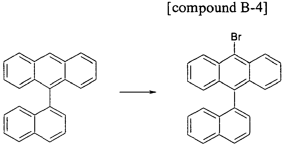
- In the Preparation of the compound B-1 of Preparation Example 101, the compound B-4 (6.49 g, 70%)) was prepared by using the same method as the preparation method of the compound B-1, except that 9-(1-naphthyl)-anthracene was used instead of 9-(2-naphthyl)-anthracene. MS:[M]+=383
-

- 9-bromoanthracene (8.2 g, 31.9 mmol), biphenyl boronic acid (7.6 g, 38.4 mmol) and Pd(PPh3)4 (0.737 g, 2 mol%) were put into 2M K2CO3 aqueous solution (300 mL) and tetrahydrofuran (300 mL), and refluxed and agitated for about 24 hours. It was cooled to normal temperature, the organic layer was separated from the reaction mixture solution, and the organic layer was dried with anhydrous magnesium sulfate, and filtered. The filtered solution was concentrated under the reduced pressure and recrystallized with tetrahydrofuran and ethanol to prepare the compound B-5 (8.5 g, 81%). MS: [M]+=330
- In the Preparation of the compound B-1 of Preparation Example 101, the compound B-6 (7.03 g, 71%)) was prepared by using the same method as the preparation method of the compound B-1, except that the compound B-5 was used instead of 9-(2-naphthyl)-anthracene. MS: [M]+ =409
-

- After 2-naphthalene boronic acid (10 g 58.1 mmol) and 2-bromo-6-naphthol (10.8 g, 48.4 mmol) were completely dissolved in tetrahydrofuran (100 mL), 2M potassium carbonate aqueous solution (100 mL) was added thereto, and tetrakistriphenylphosphino palladium (Pd(PPh3)4 (1.12 g, 2 mol%) was put thereinto, agitated and refluxed for 5 hours. The temperature was lowered to normal temperature, the water layer was removed, and it was dried with anhydrous magnesium sulfate and filtered. The filtered solution was concentrated under the reduced pressure and recrystallized with hexane and ethanol to prepare the compound B-7 (8.5 g, 65%). MS: [M+H]+=271
- After the compound B-7 (7.2 g, 26.7 mmol) was dissolved in dichloromethane, triethylamine (7.47 mL, 53.6 mmol) was added thereto, and agitated for 10 min. After the temperature was lowered to 0°C, trifluoromethanesulfonic acid ((CF3SO2)2O) (6.76 mL, 40.2 mmol) was slowly added thereto, the temperature was increased to normal temperature, and it was agitated for 1 hour. After the sodium hydrogen carbonate aqueous solution was added, the water layer was removed, and water was removed with anhydrous magnesium sulfate. The filtered solution was concentrated under the reduced pressure and recrystallized with hexane and ethanol to prepare the compound B-8 (8.69 g, 81%). MS: [M+H]+=403
-

- 1-bromonaphthalene (34.8 g, 168 mmol) was dissolved in tetrahydrofuran (170 ml), and cooled to -78°C, 2.5 M n-butyl lithium (67.3 ml, 168 mmol) was slowly added thereto, and it was agitated for 1 hour. 2-bromoanthraquinone (21 g, 73.1 mmol) was added, the temperature was increased to normal temperature, and it was agitated for 3 hours. The saturated ammonium chloride aqueous solution was added, the water layer was removed, dried with anhydrous magnesium sulfate, filtered, and dried under reduced pressure. It was recrystallized with ethylether to prepare the compound B-9 (32.5 g, 82%). MS: [M+H]+=544
- The compound B-9 (32.3 g, 59.5 mmol), potassium iodide (29.6 g, 178.4 mmol) and sodium hyphophosphite (38 g, 256.8 mmol) were put into acetic acid (100 mL), and agitated and refluxed for 3 hours. The temperature was lowered to normal temperature, the generated precipitate was filtered, and washed with water and ethanol to prepare the compound B-10(25.4 g, 84%). MS:[M]+=509
-

- In the Preparation of the compound B-9 of Preparation Example 105, the compound B-11 (31.8 g, 80%) was prepared by using the same method as the preparation method of the compound B-9, except that 2-bromonaphthalene was used instead of 1-bromonaphthalene. MS: [M+H]+ =544
- In the Preparation of the compound B-10 of Preparation Example 105, the compound B-12 (25.4 g, 84%) was prepared by using the same method as the preparation method of the compound B-10, except that the compound B-11 was used instead of the compound B-9. MS: [M]+ =509
- The compound B-13 (8.6 g, 92%) was prepared by using the same method as Preparation Example 4, except that the compound B-12 was used instead of the compound A-4 in Preparation Example 4. MS:[M+H]+ =557
-

- In the Preparation of the compound B-3 of Preparation Example 101, the compound B-14 (4.45 g, 76%) was prepared by using the same method as the preparation method of the compound B-3, except that the compound B-13 was used instead of the compound B-2. MS:[M+H]+=586
-

- Carbazole (3.34 g, 20 mmol), 1-bromo-4-iodobenzene (6.79 g, 24 mmol), potassium carbonate (K2CO3) (5.52 g, 40 mmol), copper iodide (CuI) (0.381 g, 2 mmol) and 1,10-phenanthroline (0.360 g, 2 mmol) were suspended in xylene (50 mL) and agitated and refluxed for 24 hours. After it was cooled to normal temperature, the mixture was diluted with water (100 mL), and extracted with ethylacetate. The organic extract material was dried over anhydrous magnesium sulfate and filtered. The filtered solution was concentrated under the reduced pressure and recrystallized with ethyl ether and hexane to prepare the compound B-15 (4.83 g, 75%). MS:[M+H]+=322
-

- 1-amino-2-naphthalenecarbaldehyde (0.25 g, 1.45 mmol) and 4-bromoacetophenone (2.88 g, 1.45 mmol) were dispersed in ethanol (15 mL), and 0.5 mL of the solution in which KOH was saturated and dissolved in ethanol was slowly added thereto. The mixture was agitated and refluxed for 15 hours. After it was cooled to normal temperature, the generated solid was filtered, washed with ethanol, and dried under the vacuum to prepare the compound B-16 (0.290 g, 60%). MS:[M]+=334
-

- After 1-bromo-4-iodobenzene (2.82 g, 10 mmol) and 2-phenyl-cyophenboronic acid (2.04 g, 10 mmol) were dissolved in tetrahydrofuran (30 mL), 2M potassium carbonate aqueous solution (20 mL) was added thereto, and tetrakistriphenylphosphino palladium (Pd(PPh3)4(231 mg, 2 mol%) was put thereinto, agitated and refluxed for 5 hours. The temperature was lowered to normal temperature, the water layer was removed, and the organic layer was dried with anhydrous magnesium sulfate and filtered. The filtered solution was concentrated under the reduced pressure and recrystallized with ethylether to prepare the compound B-17 (2.2 g, 70%). MS:[M]+=315
-

- Thionyl chloride (SOCl2) (20 mL) and dimethylformamide (DMF) (1 mL) were put into 6-bromo-2-naphthoic acid (5.0 g, 20 mmol), and agitated and refluxed for 4 hours. After an excessive amount of thionyl chloride (SOCl2) was removed by the vacuum distillation, N-methylpyrolidyne (NMP) (20 mL), and N-phenyl-1,2-diaminobenzene (3.7 g, 20 mmol) were put into the reaction mixture and agitated at 160°C for 12 hours. The temperature was lowered to normal temperature, and an excessive amount of water was added thereto to form a solid. It was filtered, washed with water and ethanol, and dried to prepare the compound B-18 (6.2 g, 78%). MS:[M]+=399
-

- The compound B-19 (4.54 g, 65%) was prepared by using the same method as Preparation Example 111, except that 4-bromobenzoic acid was used instead of 6-bromo-2-naphthoic acid in Preparation Example 111. MS:[M]+=349
-

- The compound B-20 (2.12 g, 75%) was prepared by using the same method as Preparation Example 110, except that 2-naphthalene boronic acid was used instead of 2-phenyl-5-cyophenboronic acid in Preparation Example 110. MS:[M]+=283
-
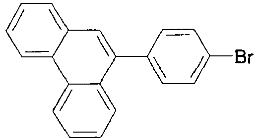
- The compound B-21 (2.33 g, 70%) was prepared by using the same method as Preparation Example 110, except that 9-phenanthrene boronic acid was used instead of 2-phenyl-5-cyophenboronic acid in Preparation Example 110. MS:[M]+=333
-

- The compound B-22 (2.14 g, 60%) was prepared by using the same method as Preparation Example 110, except that 1-pyrene boronic acid was used instead of 2-phenyl-5-cyophenboronic acid in Preparation Example 110. MS:[M]+=357
-

- 4-bromo-aniline) (1.72 g, 10 mmol), 4-iodobiphenyl) (6.72 g, 24 mmol), potassium carbonate (K2CO3) (5.52 g, 40 mmol), copper iodide (CuI) (0.381 g, 2 mmol) and 1,10-phenanthroline (0.360 g, 2 mmol) were suspended in xylene (50 mL) and agitated and refluxed for 24 hours. After it was cooled to normal temperature, the mixture was diluted with water (100 mL), and extracted with ethylacetate. The organic extract material was dried over anhydrous magnesium sulfate and filtered. The filtered solution was concentrated under the reduced pressure and recrystallized with hexane to prepare the compound B-23 (1.43 g, 30%). MS:[M]+=476
-

- The compound B-24 (1.75 g, 40%) was prepared by using the same method as Preparation Example 108, except that 1-bromo-3.5-diiodobenzene)(3.68 g, 9.0 mmol) was used instead of 1-bromo-4-iodobenzene in Preparation Example 108. MS:[M]+=487
-

- After the compound B-1 (3.83 g, 10.0 mmol) and the compound A-4 (3.94 g, 10.0 mmol) were dissolved in tetrahydrofuran (100 mL), 2M potassium carbonate aqueous solution (20 mL) was added thereto, and tetrakistriphenylphosphino palladium (Pd(PPh3)4 (231 mg, 2 mol%) was put thereinto, agitated and refluxed for 5 hours. The temperature was cooled to normal temperature, and the produced solid was filtered. The filtered solid was recrystallized with chloroform and ethanol, filtered, and dried to manufacture the compound of Formula 1-a-8 (3.88 g, 68%). MS: [M+H]+=571 <Example 2 > Preparation of the compound of Formula 2-a-6


- After the compound B-12 (5.09 g, 10.0 mmol) and the compound A-7 (4.96 g, 10.0 mmol) were dissolved in tetrahydrofuran (100 mL), 2M potassium carbonate aqueous solution (20 mL) was added thereto, and tetrakistriphenylphosphino palladium (231 mg, 2 mol%) was put thereinto, agitated and refluxed for 5 hours. The temperature was cooled to normal temperature, and the produced solid was filtered. The filtered solid was recrystallized with chloroform and ethanol, filtered, and dried to manufacture the compound of Formula 2-a-6 (5.19 g, 65%). MS: [M+H]+=799
-
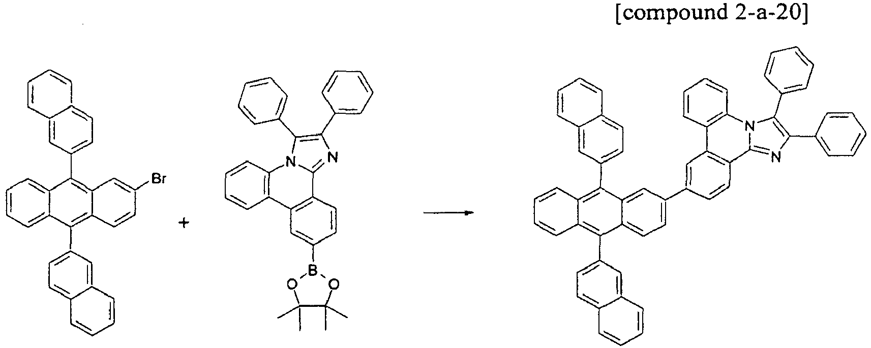
- The compound 2-a-20 (4.79 g, 60%) was prepared by using the same method as Example 2 , except that the compound A-17 (4.96 g, 10.0 mmol) was used instead of the compound A-7 in Example 2. MS: [M+H]+=799
-

- After the compound B-8 (4.02 g, 10.0 mmol) and the compound A-26-2 (4.89 g, 10.0 mmol) were dissolved in tetrahydrofuran (100 mL), 2M potassium carbonate aqueous solution (20 mL) was added thereto, and tetrakistriphenylphosphino palladium (231 mg, 2 mol%) was put thereinto, agitated and refluxed for 5 hours. The temperature was cooled to normal temperature, and the produced solid was filtered. The filtered solid was recrystallized with chloroform and ethanol, filtered, and dried to manufacture the compound of Formula 2-a-29 (4.37 g, 70%). MS: [M+H]+=625
-

- The compound 2-a-38 (3.43 g, 60%) was prepared by using the same method as Example 1, except that the compound B-20 (2.83 g, 10.0 mmol) was used instead of the compound B-1 and the compound A-17 (4.96 g, 10.0 mmol) was used instead of the compound A-4 in Example 1. MS: [M+H]+=573 <Example 6 > Preparation of the compound of Formula 2-b-6

- The compound 2-b-6 (5.57 g, 70%) was prepared by using the same method as Example 1, except that the compound B-12 (5.09 g, 10.0 mmol) was used instead of the compound B-1 and the compound A-10 (4.94 g, 10.0 mmol) was used instead of the compound A-4 in Example 1. MS: [M+H]+=797
-

- The compound 2-b-16 (3.29 g, 55%) was prepared by using the same method as Example 1, except that 2-chloro-4,6-diphenyltriazine (2.67 g, 10.0 mmol) was used instead of the compound B-1 and the compound A-10 (4.94 g, 10.0 mmol) was used instead of the compound A-4 in Example 1. MS: (M+H]+=600
-

- The compound 2-b-19 (5.57 g, 70%) was prepared by using the same method as Example 1, except that the compound B-12 (5.09 g, 10.0 mmol) was used instead of the compound B-1 and the compound A-20 (4.94 g, 10.0 mmol) was used instead of the compound A-4 in Example 1. MS: [M+H]+=797
-

- The compound 2-b-28 (4.25 g, 62%) was prepared by using the same method as Example 1, except that the compound B-18 (3.99 g, 10.0 mmol) was used instead of the compound B-1 and the compound A-20 (4.94 g, 10.0 mmol) was used instead of the compound A-4 in Example 1. MS: [M+H]+=687
- A glass substrate on which a thin film of ITO (indium tin oxide) was coated to a thickness of 1000 Å was immersed in distilled water having a detergent dissolved therein to wash the substrate with ultrasonic waves. At this time, the detergent as used herein was a product commercially available from Fisher Co. and the distilled water was one which had been twice filtered by using a filter commercially available from Millipore Co. ITO was washed for 30 minutes, and then washing with ultrasonic waves was repeated twice for 10 minutes by using distilled water. After the completion of washing with distilled water, washing with ultrasonic waves was subsequently carried out by using solvents such as isopropyl alcohol, acetone and methanol, the resultant product was dried, and transported to the plasma washing machine. In addition, after the substrate was washed for 5 min by using the oxygen plasma, the substrate was transported by using the vacuum deposition device.
- On the ITO transparent electrode thus prepared, hexanitrile hexaazatriphenylene (HAT) of the following Formula was coated to thicknesses of 500 Å by thermal vacuum deposition to form a hole injecting layer.

- 4,4'-bis[N-(1-naphthyl)-N-phenylamino]biphenyl (NPB) (400 A) of the following Formula that was the material transporting the holes was deposited under the vacuum on the hole injection layer to form the hole transport layer.


- Subsequently, GH and GD as shown below were deposited under the vacuum state at the weight ratio of 20:1 in the film thickness of 300 Å on the hole transport layer, thereby forming the light emitting layer.
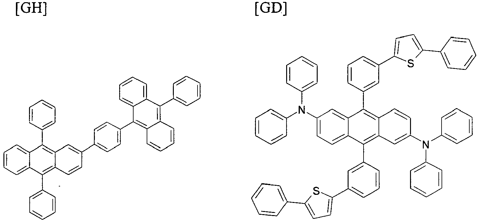
- On the light emitting layer, the compound of Formula 1-a-8 that was manufactured in Example 1 was deposited under the vacuum state in the thickness of 200 Å, thereby forming the electron injection and transport layer.
- On the electron injection and transport layer, lithium fluoride (LiF) in a thickness of 12 A and aluminium in a thickness of 2000 Å were subsequently deposited to form a cathode.
- In the above process, the deposition speed of the organic material was maintained at 0.4 to 0.7 Å/sec, the deposition speed of the lithium fluoride of the cathode was maintained at 0.3 Å/sec, the deposition speed of aluminium was maintained at 2 Å/sec, and the degree of vacuum in the deposition was maintained at 2 × 10⁻⁷ to 5 × 10⁻⁸ torr, thereby manufacturing the organic light emitting device.
- When current was applied to the organic light emitting device that was manufactured by Experimental Example 1-1-1 the results of Table 4-1 were obtained.
[Table 4-1] compound voltage (V@10mA/cm2) efficiency (cd/A @10mA/cm2) color coordinate (x,y) Experimental Example 1-1-1 1-a-8 4.03 28.02 (0.323,0.645) - In Experimental Example 1-1-1, the organic light emitting device was manufactured by using the same method as Experimental Example 1-1-1, except that the compounds described in Table 4-2 were used instead of the compound of Formula 1-a-8.
- When current was applied to the organic light emitting device that was manufactured by Experimental Examples 1-2-1 to 1-2-17 and Comparative Example 2, the results of Table 4-2 were obtained.
[Table 4-2] compound voltage (V@10mA/cm2) efficiency (cd/A @10mA/cm2) color coordinate (x,y) Experimental Example 1-2-9 2-a-6 5.57 19.29 (0.325,0.643) Experimental Example 1-2-10 2-a-20 4.32 28.23 (0.322,0.642) Experimental Example 1-2-11. 2-b-6 4.37 26.02 (0.323,0.644) Experimental Example 1-2-12 2-b-19 4.45 26.08 (0.326,0.648) Comparative Example 2 ET-A2 5.31 23.07 (0.326,0.644) - The novel heterocyclic derivative according to the present invention may be used as the material of the organic material layer of the organic electronic device, and the organic electronic device according to the present invention has excellent properties in views of an increase in efficiency, a reduction in driving voltage, a lengthened life span, and an increase in stability.
- In Experimental Example 1-1-1, the organic light emitting device was manufactured by using the same method as Experimental Example 1-1-1, except that the compound of the following Formula ET-A3 was used instead of the compound of Formula 1-a-8.

- In Experimental Example 1-1-1, the organic light emitting device was manufactured by using the same method as Experimental Example 1-4-1, except that the compounds described in Table 4-4 were used instead of the compound of Formula 1-a-8.
- When current was applied to the organic light emitting device that was manufactured by Experimental Examples 1-4-1 to 1-4-16 and Comparative Example 4, the results of Table 4-3 were obtained.
[Table 4-3] compound voltage (V@10mA/cm2) efficiency (cd/A @10mA/cm2) color coordinate (x,y) Experimental Example 1-4-5 2-b-28 5.91 24.64 (0.324,0.644) Experimental Example 1-4-9 5-a-13 6.78 22.24 (0.327,0.648) Experimental Example 1-4-10 5-a-23 5.36 18.13 (0.329,0.650) Comparative Example 4 ET-A4 7.23 19.25 (0.324,0.638) - In Tables 4-1, 4-2 and 4-3, the compounds that include the structure of Formula 3-1 or 4-1 showed characteristics of low voltage and high efficiency as compared to the compounds of Comparative Examples.
- In Experimental Example 1-1-1, the organic light emitting device was manufactured by using the same method as Experimental Example 1-1-1, except that the compounds described in the following Table 4-5 were used instead of the compound of Formula 1-a-8.
- When current was applied to the organic light emitting device that was manufactured by Experimental Examples 2-1-15 to 2-1-17 and Comparative Example 2, the results of Table 4-4 were obtained.
[Table 4-4] compound voltage (V@10mA/cm2) efficiency (cd/A @10mA/cm2) color coordinate (x,y) Experimental Example 2-1-15 2-a-29 4.53 24.28 (0.325,0.646) Experimental Example 2-1-16 2-a-38 4.35 25.47 (0.326,0.643) Experimental Example 2-1-17 2-b-16 4.73 24.48 (0.324,0.645) Comparative Example 2 ET-A2 5.31 23.07 (0.326,0.644) - In Table 4-4, since the compounds that have the structure of Formula 1 have excellent electron transport and injection ability, it was confirmed that it was capable of being used to the organic light emitting device.
- A glass substrate (corning 7059 glass) on which a thin film of ITO (indium tin oxide) was coated to a thickness of 1000 Å was immersed in distilled water having a detergent dissolved therein to wash the substrate with ultrasonic waves. The detergent as used herein was a product commercially available from Fisher Co. and the distilled water was one which had been twice filtered by using a filter commercially available from Millipore Co. ITO was washed for 30 minutes, and then washing with ultrasonic waves was repeated twice for 10 minutes by using distilled water. After the completion of washing with distilled water, washing with ultrasonic waves was carried out by using solvents such as isopropyl alcohol, acetone and methanol, and the resultant product was dried.
- On the ITO transparent electrode thus prepared, hexanitrile hexaazatriphenylene was coated to thicknesses of 500 Å by thermal vacuum deposition to form a hole injecting layer. 4,4'-bis[N-(1-naphthyl)-N-phenylamino]biphenyl (NPB) (400 Å) of the above Formula that was the material transporting the holes was deposited under the vacuum on the hole injection layer to form the hole transport layer. Subsequently, on the hole transport layer, the compound that is represented by Formula 1-a-29 and prepared in Example 6 and the D3 dopant compound of the following Formula were deposited under the vacuum at the weight ratio of 100:14, thus forming the light emitting layer (300 A). Next, the ET-A2 compound (300 Å) was deposited under the vacuum as the electron injection and transport layer. On the electron injection and transport layer, lithium fluoride (LiF) in a thickness of 12 Å and aluminum in a thickness of 2,000 Å were deposited to form a cathode, thereby manufacturing the organic light emitting device.


- In the above process, the deposition speed of the organic substance was maintained at 0.4 to 0.7 Å/sec, that of lithium fluoride was maintained at 0.2 Å/sec, and that of aluminum was maintained at 3 to 7 Å/sec.
were obtained.[Table 4-6] EML(Host:D3) voltage (V@20 mA/cm2) Current efficiency (cd/A@20 mA/cm2) Color coordinate (x,y) Comparative Example 3-1 PH 6.23 15.25 (0.369,0.600) Experimental Example 3-1-1 1-a-29 4.57 36.96 (0.380,0.589) Experimental Example 3-1-2 3-a-16 4.57 22.57 (0.354,0.611) Experimental Example 3-1-3 3-c-13 5.34 28.48 (0.360,0.607) Experimental Example 3-1-4 1-a-80 4.61 40.22 (0.354,0.609) Experimental Example 3-1-5 1-b-146 4.31 39.07 (0.362,0.607) Experimental Example 3-1-6 6-a-18 4.38 29.34 (0.361,0.607) Experimental Example 3-1-7 6-a-39 4.90 36.52 (0.360,0.608) - As shown in Table 4-6, the compound derivative that is represented by Formula according to the present invention can function as the light emitting material in the organic light emitting device and the organic electronic device, and the device according to the present invention shows excellent characteristics in views of efficiency, the driving voltage, and stability. In particular, in views of efficiency, the high light emitting characteristics are shown.
- On the ITO transparent electrode that was prepared by using the same method as Experimental Example 1-1-1, hexanitrile hexaazatriphenylene (HAT) was coated to thicknesses of 500 Å by thermal vacuum deposition to form a hole injecting layer.
- On the hole injection layer, the following compounds HT-1, HT-2, or HT-3 were deposited under the vacuum to form the hole transport layer (400 Å).


- Subsequently, BH-1 and BD as shown below were deposited under the vacuum state at the weight ratio of 25:1 in the film thickness of 300 Å on the hole transport layer, thereby forming the light emitting layer.

- Subsequently, on the light emitting layer, the compound (ETL) shown in Table 4-7 was deposited under the vacuum in the film thickness of 300 Å to form the electron injection and transport layer. On the electron injection and transport layer, lithium fluoride (LiF) in a thickness of 12 Å and aluminum in a thickness of 2000 Å were subsequently deposited to form a cathode.
- In the above process, the deposition speed of the organic material was maintained at 0.4 to 0.7 Å/sec, the deposition speed of the lithium fluoride of the cathode was maintained at 0.3 Å/sec, the deposition speed of aluminium was maintained at 2 Å/sec, and the degree of vacuum in the deposition was maintained at 2 × 10⁻⁷ to 5 × 10⁻⁸ torr, thereby manufacturing the organic light emitting device. When current was applied to the organic light emitting device that was manufactured as described above, the results of Table 4-7 were obtained.
[Table 4-7] compound (HTL) compound (ETL) voltage (V@10mA/cm2) efficiency (cd/A @10mA/cm2) color coordinate (x,y) Experimental Example 4-1-1 HT-1 1-a-8 4.27 4.62 (0.139,0.158) Experimental Example 4-1-2 HT-3 1-a-8 5.01 4.51 (0.138,0.153) Experimental Example 4-1-3 HT-1 1-a-15 3.97 4.01 (0.139,0.154) Experimental Example 4-1-4 HT-2 1-a-15 4.04 4.10 (0.139,0.154) Experimental Example 4-1-5 HT-1 1-a-58 4.10 4.67 (0.139,0.158) Experimental Example 4-1-6 HT-3 1-a-58 5.47 4.21 (0.139,0.158) Experimental Example 4-1-7 HT-1 1-b-9 4.26 4.26 (0.139,0.156) Experimental Example 4-1-8 HT-2 1-b-9 4.21 4.07 (0.139,0.157) Experimental Example 4-1-9 HT-1 1-b-32 4.17 4.89 (0.139,0.147) Experimental Example 4-1-10 HT-2 1-b-32 3.86 4.80 (0.139,0.149) Experimental Example 4-1-11 HT-1 1-b-33 4.04 4.69 (0.139,0.147) Experimental Example 4-1-12 HT-2 1-b-33 4.13 4.87 (0.139,0.150) Experimental Example 4-1-13 HT-1 1-b-80 4.02 5.01 (0.138,0.147) Experimental Example 4-1-14 HT-2 1-b-80 3.85 4.96 (0.138,0.157) Experimental Example 4-1-15 HT-2 7-a-1 4.13 4.87 (0.139,0.140) Experimental Example 4-1-16 HT-1 7-a-4 4.02 5.01 (0.138,0.157) Experimental Example 4-1-17 HT-2 7-a-6 3.85 4.96 (0.138,0.147) Experimental Example 4-1-18 HT-1 7-a-10 4.13 4.87 (0.139,0.150) Experimental Example 4-1-19 HT-2 7-a-16 4.16 5.23 (0.139,0.151) Experimental Example 4-1-20 HT-1 7-a-23 5.12 4.38 (0.139,0.147) - As shown in Table 4-7, the compound that is represented by Formula 1 according to the present invention can variously use hole injection and transport materials or the light emitting material in the organic light emitting device and the organic electronic device, and the device according to the present invention shows excellent characteristics in views of efficiency, the driving voltage, and stability.
- Like Experimental Example 1-1-1, on the ITO transparent electrode, hexanitrile hexaazatriphenylene (HAT) of the above Formula was coated to thicknesses of 500 Å by thermal vacuum deposition to form a hole injecting layer.
- 4,4'-bis[N-(1-naphthyl)-N-phenylamino]biphenyl (NPB) (400 Å) of the above Formula that was the material transporting the holes was deposited under the vacuum on the hole injection layer to form the hole transport layer.
- On the hole transport layer, after the light emitting layer was formed at the weight ratio of 25:1 by using the following Formula BH-2 as the host and the above Formula BD as the dopant in the film thickness of 300 Å, the electron injection and transport layers were formed in the thickness of 300 Å by depositing the compound of Formula 1-a-8 prepared in Example 1 and the following Formula LiQ (Lithium Quinolate) under the vacuum at the weight ratio of 1:1. On the electron injection and transport layer, lithium fluoride (LiF) in a thickness of 12 Å and aluminum in a thickness of 2,000 Å were deposited to form a cathode, thereby manufacturing the organic light emitting device.


- In Experimental Example 5-1-1, the organic light emitting device was manufactured by using the same method as Experimental Example 5-1-1, except that the compounds described in the following Table 4-8 were used instead of the compound of Formula 1-a-8.
- In Experimental Example 5-1-1, the organic light emitting device was manufactured by using the same method as Experimental Example 5-1-1, except that the compound of the above Formula ET-A1 was used instead of the compound of Formula 1-a-8.
- When current was applied to the organic light emitting device that was manufactured by Experimental Examples 5-1-1 to 5-1-8 and Comparative Example 5, the results of Table 4-8 were obtained.
[Table 4-8] compound voltage (V@10mA/cm2) efficiency (cd/A @10mA/cm2) color coordinate (x,y) Experimental Example 5-1-1 1-a-8 4.09 4.73 (0.139,0.147) Experimental Example 5-1-2 1-a-14 4.13 4.86 (0.138,0.148) Experimental Example 5-1-3 1-a-15 3.96 4.97 (0.139,0.148) Experimental Example 5-1-4 1-b-32 4.04 5.26 (0.139,0.147) Experimental Example 5-1-5 1-b-3 4.28 4.67 (0.138,0.146) Experimental Example 5-1-6 1-b-80 3.85 5.32 (0.137,0.145) Experimental Example 5-1-7 5-a-59 4.26 4.26 (0.139,0.146) Experimental Example 5-1-8 5-a-67 4.21 5.21 (0.140,0.148) Comparative Example 5 ET-A1 4.73 4.12 (0.138,0.147) - As shown in Table 4-8, the compound that is represented by Formula 1 according to the present invention can be mixed with the metal compound such as LiQ to form the electron transport layer, and the device according to the present invention showed excellent characteristics in views of efficiency, the driving voltage, and stability.
Claims (12)
- A nitrogen-containing heterocyclic derivative that is represented by the following Formula 3-1 or 4-1:

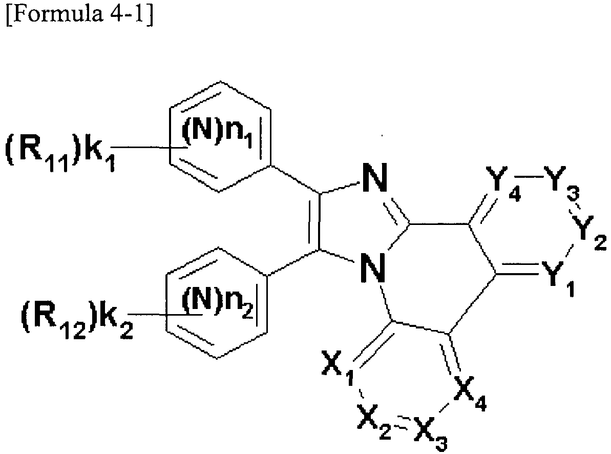 X1 is N or CR3, X2 is N or CR4, X3 is N or CR5, X4 is N or CR6, Y1 is N or CR7, Y2 is N or CR8, Y3 is N or CR9, Y4 is N or CR10, X1 to X4 and Y1 to Y4 are not simultaneously N,R3 to R12 are each independently -(L)p-(Y)q, in which p is an integer in the range of 0 to 10, q is an integer in the range of 1 to 10, and two or more adjacent groups of R3 to R12 may form a monocyclic or polycyclic ring,L is oxygen; sulfur; substituted or unsubstituted nitrogen; substituted or unsubstituted phosphorus; substituted or unsubstituted arylene group; substituted or unsubstituted alkenylene group; substituted or unsubstituted fluorenylene group; substituted or unsubstituted carbazolylene group; or substituted or unsubstituted heteroarylene group that includes one or more of N, O, and S atoms,Y is hydrogen; heavy hydrogen; halogen group; nitrile group; nitro group; hydroxy group; substituted or unsubstituted cycloalkyl group; substituted or unsubstituted alkoxy group; substituted or unsubstituted aryloxy group; substituted or unsubstituted alkylthioxy group; substituted or unsubstituted arylthioxy group; substituted or unsubstituted alkylsulfoxy group; substituted or unsubstituted arylsulfoxy group; substituted or unsubstituted alkenyl group; substituted or unsubstituted silyl group; substituted or unsubstituted boron group; substituted or unsubstituted alkylamine group; substituted or unsubstituted aralykylamine group; substituted or unsubstituted arylamine group; substituted or unsubstituted heteroarylamine group; substituted or unsubstituted aryl group; substituted or unsubstituted fluorenyl group; substituted or unsubstituted carbazole group; or substituted or unsubstituted heteroring group that includes one or more of N, O, and S atoms;in the case of when there are two or more L and Y, they are each independently the same as or different from each other,in (N)n1 and (N)n2, N means a nitrogen atom, and the nitrogen atom is used instead of a carbon atom in a benzene ring,in (N)n1, n1 is an integer in the range of 0 to 2,in (N)n2, n2 is an integer in the range of 0 to 2,k1 is an integer in the range of 0 to 4, k2 is an integer in the range of 0 to 4,in the case of when k1 is an integer of 2 or more, R11 may be different from each other, and in the case of when k2 is an integer of 2 or more, R12 may be different from each other,in the case of when X1 to X4 and Y1 to Y4 are simultaneously CR3 to CR10, at least one of R3 to R10 has a substituent group rather than hydrogen.
 - The nitrogen-containing heterocyclic derivative as set forth in claim 1, wherein the nitrogen-containing heterocyclic derivative has a structure in which two structures of Formula 3-1 or 4-1 are directly connected to each other, or connected through divalent connection group selected from the groups comprising a substituted or unsubstituted arylene group and a substituted or unsubstituted heterocyclic group.
- The nitrogen-containing heterocyclic derivative as set forth in claim 1, wherein the nitrogen-containing heterocyclic derivative is represented by the following Formulas:


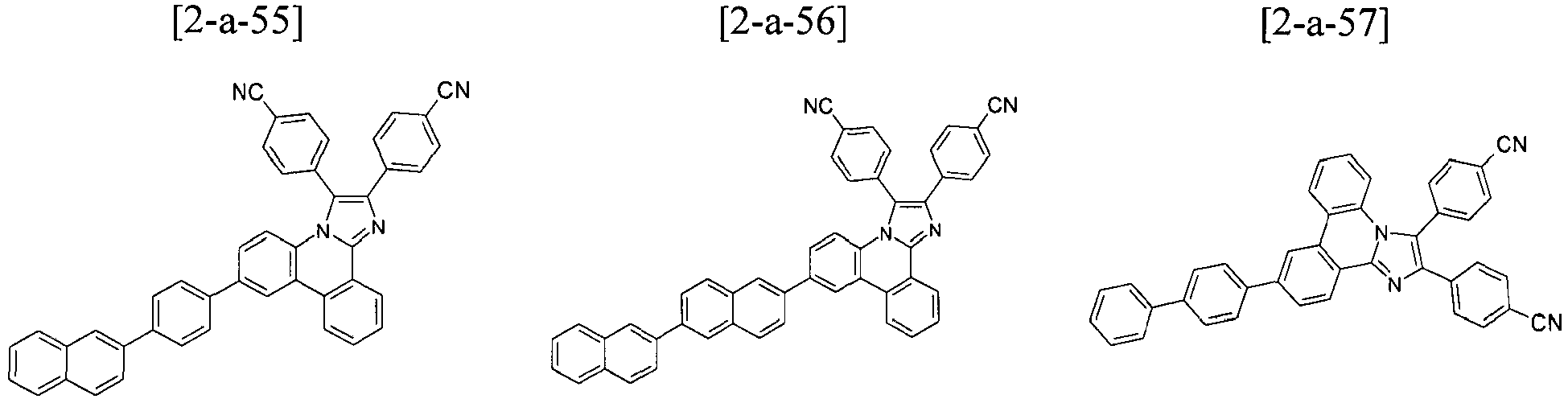


- The nitrogen-containing heterocyclic derivative as set forth in claim 1, wherein the nitrogen-containing heterocyclic derivative is represented by the following Formulas:


- The nitrogen-containing heterocyclic derivative as set forth in claim 1, wherein the nitrogen-containing heterocyclic derivative is represented by the following Formulas:


- An organic electronic device which includes a first electrode, a second electrode, and one or more organic material layers that are disposed between the first electrode and the second electrode, wherein one or more layers of the organic material layers include the nitrogen-containing heterocyclic derivative according to any one of claims 1 to 5.
- The organic electronic device as set forth in claim 6, wherein the organic material layer includes a hole injection layer or a hole transport layer, and the hole injection layer or hole transport layer includes the nitrogen-containing heterocyclic derivative.
- The organic electronic device as set forth in claim 6, wherein the organic material layer includes a light emitting layer, and the light emitting layer includes the nitrogen-containing heterocyclic derivative as a host of the light emitting layer.
- The organic electronic device as set forth in claim 6, wherein the organic material layer includes an electron transport layer, and the electron transport layer includes the nitrogen-containing heterocyclic derivative.
- The organic electronic device as set forth in claim 6, wherein the organic material layer includes an organic material layer that include the nitrogen-containing heterocyclic derivative and a hole injection layer or hole transport layer that includes a compound including arylamino group, carbazole group, or benzcarbazole group.
- The organic electronic device as set forth in claim 6, wherein the organic material layer that include the nitrogen-containing heterocyclic derivative includes the nitrogen-containing heterocyclic derivative as a host, and other organic compounds, metal or metal compounds as a dopant.
- The organic electronic device as set forth in claim 6, wherein the organic electronic device is selected from the group consisting of an organic light emitting device, an organic solar cell, an organic photoconductor (OPC) drum and an organic transistor.
Applications Claiming Priority (2)
| Application Number | Priority Date | Filing Date | Title |
|---|---|---|---|
| KR20080108602 | 2008-11-03 | ||
| EP09829272.5A EP2311826B1 (en) | 2008-11-03 | 2009-11-03 | Novel nitrogen-containing heterocyclic compound and organic electronic device using the same |
Related Parent Applications (3)
| Application Number | Title | Priority Date | Filing Date |
|---|---|---|---|
| EP09829272.5A Division EP2311826B1 (en) | 2008-11-03 | 2009-11-03 | Novel nitrogen-containing heterocyclic compound and organic electronic device using the same |
| EP09829272.5A Division-Into EP2311826B1 (en) | 2008-11-03 | 2009-11-03 | Novel nitrogen-containing heterocyclic compound and organic electronic device using the same |
| EP09829272.5 Division | 2009-11-03 |
Publications (2)
| Publication Number | Publication Date |
|---|---|
| EP2570412A1 EP2570412A1 (en) | 2013-03-20 |
| EP2570412B1 true EP2570412B1 (en) | 2017-01-04 |
Family
ID=42226220
Family Applications (2)
| Application Number | Title | Priority Date | Filing Date |
|---|---|---|---|
| EP09829272.5A Active EP2311826B1 (en) | 2008-11-03 | 2009-11-03 | Novel nitrogen-containing heterocyclic compound and organic electronic device using the same |
| EP12190141.7A Active EP2570412B1 (en) | 2008-11-03 | 2009-11-03 | Novel nitrogen-containing heterocyclic compound and organic electronic device using the same |
Family Applications Before (1)
| Application Number | Title | Priority Date | Filing Date |
|---|---|---|---|
| EP09829272.5A Active EP2311826B1 (en) | 2008-11-03 | 2009-11-03 | Novel nitrogen-containing heterocyclic compound and organic electronic device using the same |
Country Status (6)
| Country | Link |
|---|---|
| US (2) | US8368062B2 (en) |
| EP (2) | EP2311826B1 (en) |
| JP (3) | JP5801193B2 (en) |
| KR (1) | KR101052973B1 (en) |
| CN (2) | CN103333167B (en) |
| WO (1) | WO2010062065A2 (en) |
Families Citing this family (71)
| Publication number | Priority date | Publication date | Assignee | Title |
|---|---|---|---|---|
| JP5801193B2 (en) * | 2008-11-03 | 2015-10-28 | エルジー・ケム・リミテッド | New nitrogen-containing heterocyclic compounds and organic electronic devices using the same |
| AU2010214101A1 (en) | 2009-02-11 | 2011-09-01 | Sunovion Pharmaceuticals Inc. | Histamine H3 inverse agonists and antagonists and methods of use thereof |
| US8759818B2 (en) | 2009-02-27 | 2014-06-24 | E I Du Pont De Nemours And Company | Deuterated compounds for electronic applications |
| JP2012519186A (en) * | 2009-02-27 | 2012-08-23 | イー・アイ・デュポン・ドウ・ヌムール・アンド・カンパニー | Deuterium compounds for electronic applications |
| JP5509634B2 (en) * | 2009-03-16 | 2014-06-04 | コニカミノルタ株式会社 | ORGANIC ELECTROLUMINESCENT ELEMENT, DISPLAY DEVICE, LIGHTING DEVICE, AND ORGANIC ELECTROLUMINESCENT ELEMENT MATERIAL |
| KR20110008784A (en) * | 2009-07-21 | 2011-01-27 | 다우어드밴스드디스플레이머티리얼 유한회사 | Novel organic light emitting compound and organic electroluminescent device comprising same |
| DE102009053191A1 (en) * | 2009-11-06 | 2011-05-12 | Merck Patent Gmbh | Materials for electronic devices |
| EP2597094A4 (en) * | 2010-07-09 | 2014-01-08 | Idemitsu Kosan Co | IMIDAZOPYRIDINE DERIVATIVES AND ORGANIC ELECTROLUMINESCENT ELEMENTS CONTAINING THEM |
| KR101925158B1 (en) | 2010-08-02 | 2018-12-04 | 가부시키가이샤 한도오따이 에네루기 켄큐쇼 | Triazole derivative, heterocyclic compound, light-emitting element, light-emitting device, electronic device and lighting device |
| DE102010048074A1 (en) * | 2010-10-09 | 2012-04-12 | Merck Patent Gmbh | Materials for electronic devices |
| US9349964B2 (en) * | 2010-12-24 | 2016-05-24 | Lg Chem, Ltd. | Organic light emitting diode and manufacturing method thereof |
| KR101029082B1 (en) * | 2010-12-28 | 2011-04-12 | 덕산하이메탈(주) | Compound, organic electric element using same, electronic device thereof |
| KR101357191B1 (en) * | 2011-03-29 | 2014-02-04 | 대주전자재료 주식회사 | Naphthalene derivatives, material for organic electroluminescent device and organic eletroluminescent device utilizing the same |
| EP2714841B1 (en) * | 2011-06-03 | 2016-06-22 | Merck Patent GmbH | Organic electroluminescence device |
| US8999530B2 (en) | 2011-06-13 | 2015-04-07 | Lg Chem, Ltd. | Compounds and organic electronic device using same |
| CN102286278B (en) * | 2011-06-14 | 2013-10-16 | 浙江大学 | 2,3,5,6,7,8-hexa-substituted imidazole[1,2-a] pyridine fluorescent material and synthesis method thereof |
| CN103764789B (en) * | 2011-07-08 | 2016-05-25 | 株式会社Lg化学 | New compound and organic electronic device using the new compound |
| CN103718321B (en) * | 2011-08-03 | 2016-03-30 | 株式会社日本有机雷特显示器 | Organic illuminating element |
| EP2750214B1 (en) * | 2011-10-05 | 2020-06-17 | LG Chem, Ltd. | Organic light-emitting device and method for manufacturing same |
| JP5978843B2 (en) | 2012-02-02 | 2016-08-24 | コニカミノルタ株式会社 | Iridium complex compound, organic electroluminescence device material, organic electroluminescence device, lighting device and display device |
| US20140014930A1 (en) | 2012-07-13 | 2014-01-16 | Semiconductor Energy Laboratory Co., Ltd. | Organic Compound, Light-Emitting Element, Light-Emitting Device, Electronic Device, and Lighting Device |
| WO2014030666A1 (en) | 2012-08-24 | 2014-02-27 | コニカミノルタ株式会社 | Transparent electrode, electronic device, and method for manufacturing transparent electrode |
| KR102240991B1 (en) | 2012-09-12 | 2021-04-16 | 이데미쓰 고산 가부시키가이샤 | Novel compound, material for organic electroluminescence element, organic electroluminescence element, and electronic device |
| KR102116492B1 (en) | 2013-02-28 | 2020-05-29 | 삼성디스플레이 주식회사 | Compound and organic light emitting device comprising the same |
| WO2014157610A1 (en) | 2013-03-29 | 2014-10-02 | コニカミノルタ株式会社 | Organic electroluminescent element, lighting device, display device, light-emitting thin film and composition for organic electroluminescent element, and light-emitting method |
| JP6314599B2 (en) | 2013-03-29 | 2018-04-25 | コニカミノルタ株式会社 | COMPOUND FOR ORGANIC ELECTROLUMINESCENCE, ORGANIC ELECTROLUMINESCENCE ELEMENT, LIGHTING DEVICE AND DISPLAY DEVICE HAVING THE SAME |
| KR102207740B1 (en) * | 2013-08-28 | 2021-01-26 | 덕산네오룩스 주식회사 | Compound for organic electronic element, organic electronic element using the same, and an electronic device thereof |
| KR101672096B1 (en) * | 2013-09-30 | 2016-11-02 | 주식회사 엘지화학 | Heterocyclic compound and organic light emitting device comprising the same |
| KR101603387B1 (en) * | 2013-11-06 | 2016-03-14 | 주식회사 두산 | Organic compounds and organic electro luminescence device comprising the same |
| KR102167048B1 (en) | 2013-12-03 | 2020-10-19 | 삼성디스플레이 주식회사 | Compound and organic light emitting device comprising same |
| KR101641404B1 (en) * | 2013-12-17 | 2016-07-20 | 주식회사 두산 | Organic compound and organic electroluminescent device comprising the same |
| WO2015125986A1 (en) * | 2014-02-20 | 2015-08-27 | 주식회사 두산 | Organic compound and organic electroluminescent device comprising same |
| KR102235598B1 (en) * | 2014-03-11 | 2021-04-05 | 삼성디스플레이 주식회사 | Condensed cyclic compound and organic light-emitting diode comprising the same |
| US10008679B2 (en) | 2014-04-14 | 2018-06-26 | Universal Display Corporation | Organic electroluminescent materials and devices |
| US9905785B2 (en) | 2014-04-14 | 2018-02-27 | Universal Display Corporation | Organic electroluminescent materials and devices |
| US9758518B2 (en) | 2015-03-04 | 2017-09-12 | Pimera, Inc. | Compositions, uses and methods for making them |
| BR112016026150B1 (en) | 2014-05-09 | 2019-11-05 | Pimera, Inc. | carboxylic compounds and their use in the preparation of medicaments or pharmaceutical compositions for treating cancer |
| GB2528906A (en) * | 2014-08-04 | 2016-02-10 | Novaled Gmbh | Organic light emitting devices and methods |
| KR101772746B1 (en) * | 2014-08-12 | 2017-08-30 | 주식회사 엘지화학 | Organic light emitting diode |
| KR101560102B1 (en) * | 2014-11-20 | 2015-10-13 | 주식회사 엘지화학 | Organic light emitting device |
| US9793493B2 (en) * | 2014-12-30 | 2017-10-17 | Luminescence Technology Corp. | Organic material and organic electroluminescent device using the same |
| WO2016120355A2 (en) * | 2015-01-30 | 2016-08-04 | Basf Se | Herbicidal phenylpyrimidines |
| JP5831654B1 (en) | 2015-02-13 | 2015-12-09 | コニカミノルタ株式会社 | Aromatic heterocycle derivative, organic electroluminescence device using the same, illumination device and display device |
| JP6512301B2 (en) * | 2015-03-05 | 2019-05-15 | エルジー・ケム・リミテッド | Heterocyclic compound and organic light emitting device containing the same |
| KR102261644B1 (en) | 2015-03-11 | 2021-06-08 | 삼성디스플레이 주식회사 | An organic light emitting device |
| KR102423171B1 (en) * | 2015-03-16 | 2022-07-21 | 삼성디스플레이 주식회사 | Organic light emitting device and display device having the same |
| KR101778446B1 (en) * | 2015-06-05 | 2017-09-14 | 주식회사 엘지화학 | Compound and organic electronic device using the same |
| JP6447851B2 (en) * | 2015-06-19 | 2019-01-09 | エルジー・ケム・リミテッド | Organic light emitting device |
| WO2017052225A1 (en) * | 2015-09-25 | 2017-03-30 | 주식회사 엘지화학 | Organic light emitting diode |
| KR20180079328A (en) * | 2015-11-04 | 2018-07-10 | 이데미쓰 고산 가부시키가이샤 | Benzimidazole condensed heteroaryl |
| JP6788314B2 (en) | 2016-01-06 | 2020-11-25 | コニカミノルタ株式会社 | Organic electroluminescence element, manufacturing method of organic electroluminescence element, display device and lighting device |
| KR102543683B1 (en) * | 2016-03-03 | 2023-06-15 | 덕산네오룩스 주식회사 | Compound for organic electric element, organic electric element using the same, and an electronic device thereof |
| JP6750783B2 (en) * | 2016-03-30 | 2020-09-02 | エルジー・ケム・リミテッド | Compound and organic light emitting device using the same |
| KR102046930B1 (en) * | 2016-05-03 | 2019-11-20 | 주식회사 엘지화학 | Modifying agent and modified conjugated diene polymer prepared by using the same |
| KR102005867B1 (en) * | 2016-06-17 | 2019-07-31 | 삼성에스디아이 주식회사 | Composition for organic optoelectronic device and organic optoelectronic device and display device |
| KR102530705B1 (en) | 2016-11-04 | 2023-05-11 | 롬엔드하스전자재료코리아유한회사 | Organic electroluminescent compound and organic electroluminescent device comprising the same |
| JP2018127424A (en) * | 2017-02-10 | 2018-08-16 | 国立大学法人山形大学 | Novel imidazole derivative and organic EL device using the same |
| TWI764984B (en) * | 2017-02-28 | 2022-05-21 | 南韓商羅門哈斯電子材料韓國公司 | Organic electroluminescent compound and organic electroluminescent device comprising the same |
| KR102331322B1 (en) * | 2017-03-08 | 2021-11-24 | 주식회사 엘지화학 | Organic light emitting device |
| JP2020512975A (en) | 2017-03-28 | 2020-04-30 | ピメラ,インク. | Novel crystal form of POL1 inhibitor |
| CN109037446B (en) * | 2017-11-23 | 2020-02-21 | 北京鼎材科技有限公司 | Compounds and their applications in the field of organic electroluminescence |
| CN107935936A (en) * | 2017-11-29 | 2018-04-20 | 华南理工大学 | Benzimidazole compound and derivative, Organic Electron Transport Material and its preparation and application |
| KR20190114778A (en) | 2018-03-29 | 2019-10-10 | 롬엔드하스전자재료코리아유한회사 | Organic electroluminescent compound and organic electroluminescent device comprising the same |
| CN109320528B (en) * | 2018-10-27 | 2021-04-13 | 湖北大学 | Triheteroaryl free radical capable of stably emitting light at room temperature, and preparation method and application thereof |
| EP3799143B1 (en) * | 2019-09-26 | 2024-09-11 | Novaled GmbH | First and second organic semiconductor layer and organic electronic device comprising the same |
| CN113444090B (en) * | 2020-03-24 | 2024-04-16 | 北京鼎材科技有限公司 | A compound and its application |
| KR20210131079A (en) * | 2020-04-23 | 2021-11-02 | 삼성에스디아이 주식회사 | Compound for organic optoelectronic device, composition for organic optoelectronic device, organic optoelectronic device and display device |
| CN113943289B (en) * | 2020-07-15 | 2025-01-28 | 北京鼎材科技有限公司 | Organic compounds and their applications, organic electroluminescent devices |
| CN112341458B (en) * | 2020-09-29 | 2023-04-07 | 烟台显华化工科技有限公司 | Electron transport material, organic electroluminescent device and display device |
| US20230416264A1 (en) | 2020-12-02 | 2023-12-28 | Merck Patent Gmbh | Heterocyclic compounds for organic electroluminescent devices |
| CN117843637A (en) * | 2023-12-28 | 2024-04-09 | 京东方科技集团股份有限公司 | Imidazole derivative, organic electroluminescent material, organic light-emitting layer host material, organic electroluminescent device and display panel |
Family Cites Families (9)
| Publication number | Priority date | Publication date | Assignee | Title |
|---|---|---|---|---|
| KR100691543B1 (en) | 2002-01-18 | 2007-03-09 | 주식회사 엘지화학 | New material for electron transport and organic light emitting device using the same |
| KR20040072004A (en) * | 2003-02-07 | 2004-08-16 | 삼성에스디아이 주식회사 | Emitting compound for electroluminescence device and device using thereof |
| KR20080028425A (en) * | 2005-07-11 | 2008-03-31 | 이데미쓰 고산 가부시키가이샤 | Nitrogen-containing heterocyclic derivatives having electron-withdrawing substituents and organic electroluminescent devices using them |
| KR100890862B1 (en) * | 2005-11-07 | 2009-03-27 | 주식회사 엘지화학 | Organic electroluminescent device and method for preparing the same |
| JP5324229B2 (en) * | 2006-02-10 | 2013-10-23 | ユニバーサル ディスプレイ コーポレイション | Metal complexes of cyclometalated imidazo [1,2-f] phenanthridine and diimidazo [1,2-a: 1 ', 2'-c] quinazoline ligands and their isoelectronic and benzofused analogs |
| KR100851519B1 (en) | 2006-12-20 | 2008-08-11 | 부산대학교 산학협력단 | Iridium complex compound with improved luminescence properties and organic light emitting device comprising the same |
| KR100831356B1 (en) | 2006-12-21 | 2008-05-21 | (재)대구경북과학기술연구원 | Phenanthridine Derivative Compound and Organic Electroluminescent Device Using the Same |
| WO2008156879A1 (en) * | 2007-06-20 | 2008-12-24 | Universal Display Corporation | Blue phosphorescent imidazophenanthridine materials |
| JP5801193B2 (en) | 2008-11-03 | 2015-10-28 | エルジー・ケム・リミテッド | New nitrogen-containing heterocyclic compounds and organic electronic devices using the same |
-
2009
- 2009-11-03 JP JP2011518668A patent/JP5801193B2/en active Active
- 2009-11-03 CN CN201310225172.4A patent/CN103333167B/en active Active
- 2009-11-03 CN CN200980131071.2A patent/CN102119158B/en active Active
- 2009-11-03 WO PCT/KR2009/006437 patent/WO2010062065A2/en not_active Ceased
- 2009-11-03 US US13/054,047 patent/US8368062B2/en active Active
- 2009-11-03 EP EP09829272.5A patent/EP2311826B1/en active Active
- 2009-11-03 KR KR1020097023115A patent/KR101052973B1/en active Active
- 2009-11-03 EP EP12190141.7A patent/EP2570412B1/en active Active
-
2011
- 2011-09-23 US US13/243,022 patent/US9139562B2/en active Active
-
2013
- 2013-06-27 JP JP2013134710A patent/JP5838183B2/en active Active
-
2014
- 2014-01-06 JP JP2014000409A patent/JP2014131999A/en active Pending
Non-Patent Citations (1)
| Title |
|---|
| None * |
Also Published As
| Publication number | Publication date |
|---|---|
| CN102119158A (en) | 2011-07-06 |
| CN102119158B (en) | 2015-09-09 |
| CN103333167B (en) | 2016-08-24 |
| EP2311826A2 (en) | 2011-04-20 |
| US20110127513A1 (en) | 2011-06-02 |
| KR20100062973A (en) | 2010-06-10 |
| JP2014131999A (en) | 2014-07-17 |
| US8368062B2 (en) | 2013-02-05 |
| WO2010062065A2 (en) | 2010-06-03 |
| CN103333167A (en) | 2013-10-02 |
| US9139562B2 (en) | 2015-09-22 |
| JP5801193B2 (en) | 2015-10-28 |
| JP2014015460A (en) | 2014-01-30 |
| EP2570412A1 (en) | 2013-03-20 |
| JP5838183B2 (en) | 2016-01-06 |
| KR101052973B1 (en) | 2011-07-29 |
| EP2311826A4 (en) | 2012-04-25 |
| US20120007069A1 (en) | 2012-01-12 |
| WO2010062065A3 (en) | 2010-08-26 |
| JP2011528033A (en) | 2011-11-10 |
| EP2311826B1 (en) | 2017-05-24 |
Similar Documents
| Publication | Publication Date | Title |
|---|---|---|
| EP2311826B1 (en) | Novel nitrogen-containing heterocyclic compound and organic electronic device using the same | |
| EP2719742B1 (en) | Novel compounds and organic electronic device using same | |
| EP2749560B1 (en) | Novel nitrogen-containing heterocyclic compounds and organic electronic device using same | |
| EP2730634B1 (en) | Novel compound and organic electronic device using same | |
| TWI651312B (en) | Organic compound and organic optoelectric device and? display device | |
| US8344368B2 (en) | Fused cyclic compound and organic electronic device | |
| EP2876104B1 (en) | Polycyclic compound and organic electronic device comprising same | |
| EP3327024B1 (en) | Heterocyclic compound and organic light emitting diode comprising same | |
| EP2937347B1 (en) | Novel compound and organic electronic element using same | |
| KR101104546B1 (en) | New nitrogen-containing heterocyclic compounds and organic electronic device using the same | |
| EP3263555A1 (en) | Hetero ring compound and organic luminescent element comprising same | |
| CN112969695A (en) | Compound and organic light emitting device including the same | |
| KR101578475B1 (en) | Compound Containing Dibenzothiophene, Arylamine Derivatives And Organic Electronic Element Using The Same, Terminal Thereof | |
| CN114751888B (en) | Electron transport material, preparation method thereof, light-emitting device and light-emitting device | |
| CN107880045A (en) | Compound for organic photoelectric device, the composition for organic photoelectric device and organic photoelectric device and display device |
Legal Events
| Date | Code | Title | Description |
|---|---|---|---|
| PUAI | Public reference made under article 153(3) epc to a published international application that has entered the european phase |
Free format text: ORIGINAL CODE: 0009012 |
|
| AC | Divisional application: reference to earlier application |
Ref document number: 2311826 Country of ref document: EP Kind code of ref document: P |
|
| AK | Designated contracting states |
Kind code of ref document: A1 Designated state(s): AT BE BG CH CY CZ DE DK EE ES FI FR GB GR HR HU IE IS IT LI LT LU LV MC MK MT NL NO PL PT RO SE SI SK SM TR |
|
| 17P | Request for examination filed |
Effective date: 20130821 |
|
| RBV | Designated contracting states (corrected) |
Designated state(s): AT BE BG CH CY CZ DE DK EE ES FI FR GB GR HR HU IE IS IT LI LT LU LV MC MK MT NL NO PL PT RO SE SI SK SM TR |
|
| 17Q | First examination report despatched |
Effective date: 20140602 |
|
| RIC1 | Information provided on ipc code assigned before grant |
Ipc: C07D 401/04 20060101ALI20150417BHEP Ipc: H01L 51/00 20060101ALI20150417BHEP Ipc: C07D 401/14 20060101ALI20150417BHEP Ipc: C07D 403/14 20060101AFI20150417BHEP |
|
| GRAP | Despatch of communication of intention to grant a patent |
Free format text: ORIGINAL CODE: EPIDOSNIGR1 |
|
| INTG | Intention to grant announced |
Effective date: 20160909 |
|
| GRAS | Grant fee paid |
Free format text: ORIGINAL CODE: EPIDOSNIGR3 |
|
| GRAA | (expected) grant |
Free format text: ORIGINAL CODE: 0009210 |
|
| AC | Divisional application: reference to earlier application |
Ref document number: 2311826 Country of ref document: EP Kind code of ref document: P |
|
| AK | Designated contracting states |
Kind code of ref document: B1 Designated state(s): AT BE BG CH CY CZ DE DK EE ES FI FR GB GR HR HU IE IS IT LI LT LU LV MC MK MT NL NO PL PT RO SE SI SK SM TR |
|
| REG | Reference to a national code |
Ref country code: GB Ref legal event code: FG4D |
|
| REG | Reference to a national code |
Ref country code: CH Ref legal event code: EP |
|
| REG | Reference to a national code |
Ref country code: AT Ref legal event code: REF Ref document number: 859126 Country of ref document: AT Kind code of ref document: T Effective date: 20170115 |
|
| REG | Reference to a national code |
Ref country code: IE Ref legal event code: FG4D |
|
| REG | Reference to a national code |
Ref country code: DE Ref legal event code: R096 Ref document number: 602009043628 Country of ref document: DE |
|
| REG | Reference to a national code |
Ref country code: LT Ref legal event code: MG4D Ref country code: NL Ref legal event code: MP Effective date: 20170104 |
|
| REG | Reference to a national code |
Ref country code: AT Ref legal event code: MK05 Ref document number: 859126 Country of ref document: AT Kind code of ref document: T Effective date: 20170104 |
|
| PG25 | Lapsed in a contracting state [announced via postgrant information from national office to epo] |
Ref country code: NL Free format text: LAPSE BECAUSE OF FAILURE TO SUBMIT A TRANSLATION OF THE DESCRIPTION OR TO PAY THE FEE WITHIN THE PRESCRIBED TIME-LIMIT Effective date: 20170104 |
|
| PG25 | Lapsed in a contracting state [announced via postgrant information from national office to epo] |
Ref country code: GR Free format text: LAPSE BECAUSE OF FAILURE TO SUBMIT A TRANSLATION OF THE DESCRIPTION OR TO PAY THE FEE WITHIN THE PRESCRIBED TIME-LIMIT Effective date: 20170405 Ref country code: FI Free format text: LAPSE BECAUSE OF FAILURE TO SUBMIT A TRANSLATION OF THE DESCRIPTION OR TO PAY THE FEE WITHIN THE PRESCRIBED TIME-LIMIT Effective date: 20170104 Ref country code: IS Free format text: LAPSE BECAUSE OF FAILURE TO SUBMIT A TRANSLATION OF THE DESCRIPTION OR TO PAY THE FEE WITHIN THE PRESCRIBED TIME-LIMIT Effective date: 20170504 Ref country code: HR Free format text: LAPSE BECAUSE OF FAILURE TO SUBMIT A TRANSLATION OF THE DESCRIPTION OR TO PAY THE FEE WITHIN THE PRESCRIBED TIME-LIMIT Effective date: 20170104 Ref country code: NO Free format text: LAPSE BECAUSE OF FAILURE TO SUBMIT A TRANSLATION OF THE DESCRIPTION OR TO PAY THE FEE WITHIN THE PRESCRIBED TIME-LIMIT Effective date: 20170404 Ref country code: LT Free format text: LAPSE BECAUSE OF FAILURE TO SUBMIT A TRANSLATION OF THE DESCRIPTION OR TO PAY THE FEE WITHIN THE PRESCRIBED TIME-LIMIT Effective date: 20170104 |
|
| PG25 | Lapsed in a contracting state [announced via postgrant information from national office to epo] |
Ref country code: AT Free format text: LAPSE BECAUSE OF FAILURE TO SUBMIT A TRANSLATION OF THE DESCRIPTION OR TO PAY THE FEE WITHIN THE PRESCRIBED TIME-LIMIT Effective date: 20170104 Ref country code: ES Free format text: LAPSE BECAUSE OF FAILURE TO SUBMIT A TRANSLATION OF THE DESCRIPTION OR TO PAY THE FEE WITHIN THE PRESCRIBED TIME-LIMIT Effective date: 20170104 Ref country code: PT Free format text: LAPSE BECAUSE OF FAILURE TO SUBMIT A TRANSLATION OF THE DESCRIPTION OR TO PAY THE FEE WITHIN THE PRESCRIBED TIME-LIMIT Effective date: 20170504 Ref country code: PL Free format text: LAPSE BECAUSE OF FAILURE TO SUBMIT A TRANSLATION OF THE DESCRIPTION OR TO PAY THE FEE WITHIN THE PRESCRIBED TIME-LIMIT Effective date: 20170104 Ref country code: LV Free format text: LAPSE BECAUSE OF FAILURE TO SUBMIT A TRANSLATION OF THE DESCRIPTION OR TO PAY THE FEE WITHIN THE PRESCRIBED TIME-LIMIT Effective date: 20170104 Ref country code: BG Free format text: LAPSE BECAUSE OF FAILURE TO SUBMIT A TRANSLATION OF THE DESCRIPTION OR TO PAY THE FEE WITHIN THE PRESCRIBED TIME-LIMIT Effective date: 20170404 Ref country code: SE Free format text: LAPSE BECAUSE OF FAILURE TO SUBMIT A TRANSLATION OF THE DESCRIPTION OR TO PAY THE FEE WITHIN THE PRESCRIBED TIME-LIMIT Effective date: 20170104 |
|
| REG | Reference to a national code |
Ref country code: DE Ref legal event code: R097 Ref document number: 602009043628 Country of ref document: DE |
|
| REG | Reference to a national code |
Ref country code: FR Ref legal event code: PLFP Year of fee payment: 9 |
|
| PG25 | Lapsed in a contracting state [announced via postgrant information from national office to epo] |
Ref country code: IT Free format text: LAPSE BECAUSE OF FAILURE TO SUBMIT A TRANSLATION OF THE DESCRIPTION OR TO PAY THE FEE WITHIN THE PRESCRIBED TIME-LIMIT Effective date: 20170104 Ref country code: CZ Free format text: LAPSE BECAUSE OF FAILURE TO SUBMIT A TRANSLATION OF THE DESCRIPTION OR TO PAY THE FEE WITHIN THE PRESCRIBED TIME-LIMIT Effective date: 20170104 Ref country code: EE Free format text: LAPSE BECAUSE OF FAILURE TO SUBMIT A TRANSLATION OF THE DESCRIPTION OR TO PAY THE FEE WITHIN THE PRESCRIBED TIME-LIMIT Effective date: 20170104 Ref country code: RO Free format text: LAPSE BECAUSE OF FAILURE TO SUBMIT A TRANSLATION OF THE DESCRIPTION OR TO PAY THE FEE WITHIN THE PRESCRIBED TIME-LIMIT Effective date: 20170104 Ref country code: SK Free format text: LAPSE BECAUSE OF FAILURE TO SUBMIT A TRANSLATION OF THE DESCRIPTION OR TO PAY THE FEE WITHIN THE PRESCRIBED TIME-LIMIT Effective date: 20170104 |
|
| PLBE | No opposition filed within time limit |
Free format text: ORIGINAL CODE: 0009261 |
|
| STAA | Information on the status of an ep patent application or granted ep patent |
Free format text: STATUS: NO OPPOSITION FILED WITHIN TIME LIMIT |
|
| PG25 | Lapsed in a contracting state [announced via postgrant information from national office to epo] |
Ref country code: DK Free format text: LAPSE BECAUSE OF FAILURE TO SUBMIT A TRANSLATION OF THE DESCRIPTION OR TO PAY THE FEE WITHIN THE PRESCRIBED TIME-LIMIT Effective date: 20170104 Ref country code: SM Free format text: LAPSE BECAUSE OF FAILURE TO SUBMIT A TRANSLATION OF THE DESCRIPTION OR TO PAY THE FEE WITHIN THE PRESCRIBED TIME-LIMIT Effective date: 20170104 |
|
| 26N | No opposition filed |
Effective date: 20171005 |
|
| PG25 | Lapsed in a contracting state [announced via postgrant information from national office to epo] |
Ref country code: SI Free format text: LAPSE BECAUSE OF FAILURE TO SUBMIT A TRANSLATION OF THE DESCRIPTION OR TO PAY THE FEE WITHIN THE PRESCRIBED TIME-LIMIT Effective date: 20170104 |
|
| PG25 | Lapsed in a contracting state [announced via postgrant information from national office to epo] |
Ref country code: MC Free format text: LAPSE BECAUSE OF FAILURE TO SUBMIT A TRANSLATION OF THE DESCRIPTION OR TO PAY THE FEE WITHIN THE PRESCRIBED TIME-LIMIT Effective date: 20170104 |
|
| PG25 | Lapsed in a contracting state [announced via postgrant information from national office to epo] |
Ref country code: CH Free format text: LAPSE BECAUSE OF NON-PAYMENT OF DUE FEES Effective date: 20171130 Ref country code: LI Free format text: LAPSE BECAUSE OF NON-PAYMENT OF DUE FEES Effective date: 20171130 |
|
| PG25 | Lapsed in a contracting state [announced via postgrant information from national office to epo] |
Ref country code: LU Free format text: LAPSE BECAUSE OF NON-PAYMENT OF DUE FEES Effective date: 20171103 |
|
| REG | Reference to a national code |
Ref country code: BE Ref legal event code: MM Effective date: 20171130 |
|
| REG | Reference to a national code |
Ref country code: IE Ref legal event code: MM4A |
|
| PG25 | Lapsed in a contracting state [announced via postgrant information from national office to epo] |
Ref country code: MT Free format text: LAPSE BECAUSE OF NON-PAYMENT OF DUE FEES Effective date: 20171103 |
|
| REG | Reference to a national code |
Ref country code: FR Ref legal event code: PLFP Year of fee payment: 10 |
|
| PG25 | Lapsed in a contracting state [announced via postgrant information from national office to epo] |
Ref country code: IE Free format text: LAPSE BECAUSE OF NON-PAYMENT OF DUE FEES Effective date: 20171103 |
|
| PG25 | Lapsed in a contracting state [announced via postgrant information from national office to epo] |
Ref country code: BE Free format text: LAPSE BECAUSE OF NON-PAYMENT OF DUE FEES Effective date: 20171130 |
|
| PG25 | Lapsed in a contracting state [announced via postgrant information from national office to epo] |
Ref country code: HU Free format text: LAPSE BECAUSE OF FAILURE TO SUBMIT A TRANSLATION OF THE DESCRIPTION OR TO PAY THE FEE WITHIN THE PRESCRIBED TIME-LIMIT; INVALID AB INITIO Effective date: 20091103 |
|
| PG25 | Lapsed in a contracting state [announced via postgrant information from national office to epo] |
Ref country code: CY Free format text: LAPSE BECAUSE OF NON-PAYMENT OF DUE FEES Effective date: 20170104 |
|
| PG25 | Lapsed in a contracting state [announced via postgrant information from national office to epo] |
Ref country code: MK Free format text: LAPSE BECAUSE OF FAILURE TO SUBMIT A TRANSLATION OF THE DESCRIPTION OR TO PAY THE FEE WITHIN THE PRESCRIBED TIME-LIMIT Effective date: 20170104 |
|
| PG25 | Lapsed in a contracting state [announced via postgrant information from national office to epo] |
Ref country code: TR Free format text: LAPSE BECAUSE OF FAILURE TO SUBMIT A TRANSLATION OF THE DESCRIPTION OR TO PAY THE FEE WITHIN THE PRESCRIBED TIME-LIMIT Effective date: 20170104 |
|
| PGFP | Annual fee paid to national office [announced via postgrant information from national office to epo] |
Ref country code: DE Payment date: 20251020 Year of fee payment: 17 |
|
| PGFP | Annual fee paid to national office [announced via postgrant information from national office to epo] |
Ref country code: GB Payment date: 20251023 Year of fee payment: 17 |
|
| PGFP | Annual fee paid to national office [announced via postgrant information from national office to epo] |
Ref country code: FR Payment date: 20251021 Year of fee payment: 17 |