EP2567004B1 - Substrate for epitaxial growth - Google Patents
Substrate for epitaxial growth Download PDFInfo
- Publication number
- EP2567004B1 EP2567004B1 EP20110717334 EP11717334A EP2567004B1 EP 2567004 B1 EP2567004 B1 EP 2567004B1 EP 20110717334 EP20110717334 EP 20110717334 EP 11717334 A EP11717334 A EP 11717334A EP 2567004 B1 EP2567004 B1 EP 2567004B1
- Authority
- EP
- European Patent Office
- Prior art keywords
- flat surfaces
- flat
- flat surface
- disorientation
- substrate
- Prior art date
- Legal status (The legal status is an assumption and is not a legal conclusion. Google has not performed a legal analysis and makes no representation as to the accuracy of the status listed.)
- Active
Links
Images



Classifications
-
- C—CHEMISTRY; METALLURGY
- C30—CRYSTAL GROWTH
- C30B—SINGLE-CRYSTAL GROWTH; UNIDIRECTIONAL SOLIDIFICATION OF EUTECTIC MATERIAL OR UNIDIRECTIONAL DEMIXING OF EUTECTOID MATERIAL; REFINING BY ZONE-MELTING OF MATERIAL; PRODUCTION OF A HOMOGENEOUS POLYCRYSTALLINE MATERIAL WITH DEFINED STRUCTURE; SINGLE CRYSTALS OR HOMOGENEOUS POLYCRYSTALLINE MATERIAL WITH DEFINED STRUCTURE; AFTER-TREATMENT OF SINGLE CRYSTALS OR A HOMOGENEOUS POLYCRYSTALLINE MATERIAL WITH DEFINED STRUCTURE; APPARATUS THEREFOR
- C30B29/00—Single crystals or homogeneous polycrystalline material with defined structure characterised by the material or by their shape
- C30B29/10—Inorganic compounds or compositions
- C30B29/40—AIIIBV compounds wherein A is B, Al, Ga, In or Tl and B is N, P, As, Sb or Bi
- C30B29/403—AIII-nitrides
- C30B29/406—Gallium nitride
-
- B—PERFORMING OPERATIONS; TRANSPORTING
- B82—NANOTECHNOLOGY
- B82Y—SPECIFIC USES OR APPLICATIONS OF NANOSTRUCTURES; MEASUREMENT OR ANALYSIS OF NANOSTRUCTURES; MANUFACTURE OR TREATMENT OF NANOSTRUCTURES
- B82Y20/00—Nanooptics, e.g. quantum optics or photonic crystals
-
- C—CHEMISTRY; METALLURGY
- C30—CRYSTAL GROWTH
- C30B—SINGLE-CRYSTAL GROWTH; UNIDIRECTIONAL SOLIDIFICATION OF EUTECTIC MATERIAL OR UNIDIRECTIONAL DEMIXING OF EUTECTOID MATERIAL; REFINING BY ZONE-MELTING OF MATERIAL; PRODUCTION OF A HOMOGENEOUS POLYCRYSTALLINE MATERIAL WITH DEFINED STRUCTURE; SINGLE CRYSTALS OR HOMOGENEOUS POLYCRYSTALLINE MATERIAL WITH DEFINED STRUCTURE; AFTER-TREATMENT OF SINGLE CRYSTALS OR A HOMOGENEOUS POLYCRYSTALLINE MATERIAL WITH DEFINED STRUCTURE; APPARATUS THEREFOR
- C30B25/00—Single-crystal growth by chemical reaction of reactive gases, e.g. chemical vapour-deposition growth
- C30B25/02—Epitaxial-layer growth
- C30B25/18—Epitaxial-layer growth characterised by the substrate
-
- C—CHEMISTRY; METALLURGY
- C30—CRYSTAL GROWTH
- C30B—SINGLE-CRYSTAL GROWTH; UNIDIRECTIONAL SOLIDIFICATION OF EUTECTIC MATERIAL OR UNIDIRECTIONAL DEMIXING OF EUTECTOID MATERIAL; REFINING BY ZONE-MELTING OF MATERIAL; PRODUCTION OF A HOMOGENEOUS POLYCRYSTALLINE MATERIAL WITH DEFINED STRUCTURE; SINGLE CRYSTALS OR HOMOGENEOUS POLYCRYSTALLINE MATERIAL WITH DEFINED STRUCTURE; AFTER-TREATMENT OF SINGLE CRYSTALS OR A HOMOGENEOUS POLYCRYSTALLINE MATERIAL WITH DEFINED STRUCTURE; APPARATUS THEREFOR
- C30B33/00—After-treatment of single crystals or homogeneous polycrystalline material with defined structure
-
- C—CHEMISTRY; METALLURGY
- C30—CRYSTAL GROWTH
- C30B—SINGLE-CRYSTAL GROWTH; UNIDIRECTIONAL SOLIDIFICATION OF EUTECTIC MATERIAL OR UNIDIRECTIONAL DEMIXING OF EUTECTOID MATERIAL; REFINING BY ZONE-MELTING OF MATERIAL; PRODUCTION OF A HOMOGENEOUS POLYCRYSTALLINE MATERIAL WITH DEFINED STRUCTURE; SINGLE CRYSTALS OR HOMOGENEOUS POLYCRYSTALLINE MATERIAL WITH DEFINED STRUCTURE; AFTER-TREATMENT OF SINGLE CRYSTALS OR A HOMOGENEOUS POLYCRYSTALLINE MATERIAL WITH DEFINED STRUCTURE; APPARATUS THEREFOR
- C30B33/00—After-treatment of single crystals or homogeneous polycrystalline material with defined structure
- C30B33/08—Etching
- C30B33/12—Etching in gas atmosphere or plasma
-
- H—ELECTRICITY
- H01—ELECTRIC ELEMENTS
- H01S—DEVICES USING THE PROCESS OF LIGHT AMPLIFICATION BY STIMULATED EMISSION OF RADIATION [LASER] TO AMPLIFY OR GENERATE LIGHT; DEVICES USING STIMULATED EMISSION OF ELECTROMAGNETIC RADIATION IN WAVE RANGES OTHER THAN OPTICAL
- H01S5/00—Semiconductor lasers
- H01S5/30—Structure or shape of the active region; Materials used for the active region
- H01S5/32—Structure or shape of the active region; Materials used for the active region comprising PN junctions, e.g. hetero- or double- heterostructures
- H01S5/3202—Structure or shape of the active region; Materials used for the active region comprising PN junctions, e.g. hetero- or double- heterostructures grown on specifically orientated substrates, or using orientation dependent growth
- H01S5/320225—Structure or shape of the active region; Materials used for the active region comprising PN junctions, e.g. hetero- or double- heterostructures grown on specifically orientated substrates, or using orientation dependent growth polar orientation
-
- H—ELECTRICITY
- H01—ELECTRIC ELEMENTS
- H01S—DEVICES USING THE PROCESS OF LIGHT AMPLIFICATION BY STIMULATED EMISSION OF RADIATION [LASER] TO AMPLIFY OR GENERATE LIGHT; DEVICES USING STIMULATED EMISSION OF ELECTROMAGNETIC RADIATION IN WAVE RANGES OTHER THAN OPTICAL
- H01S5/00—Semiconductor lasers
- H01S5/30—Structure or shape of the active region; Materials used for the active region
- H01S5/34—Structure or shape of the active region; Materials used for the active region comprising quantum well or superlattice structures, e.g. single quantum well [SQW] lasers, multiple quantum well [MQW] lasers or graded index separate confinement heterostructure [GRINSCH] lasers
- H01S5/343—Structure or shape of the active region; Materials used for the active region comprising quantum well or superlattice structures, e.g. single quantum well [SQW] lasers, multiple quantum well [MQW] lasers or graded index separate confinement heterostructure [GRINSCH] lasers in AIIIBV compounds, e.g. AlGaAs-laser, InP-based laser
- H01S5/34333—Structure or shape of the active region; Materials used for the active region comprising quantum well or superlattice structures, e.g. single quantum well [SQW] lasers, multiple quantum well [MQW] lasers or graded index separate confinement heterostructure [GRINSCH] lasers in AIIIBV compounds, e.g. AlGaAs-laser, InP-based laser with a well layer based on Ga(In)N or Ga(In)P, e.g. blue laser
-
- H—ELECTRICITY
- H10—SEMICONDUCTOR DEVICES; ELECTRIC SOLID-STATE DEVICES NOT OTHERWISE PROVIDED FOR
- H10D—INORGANIC ELECTRIC SEMICONDUCTOR DEVICES
- H10D62/00—Semiconductor bodies, or regions thereof, of devices having potential barriers
- H10D62/80—Semiconductor bodies, or regions thereof, of devices having potential barriers characterised by the materials
- H10D62/85—Semiconductor bodies, or regions thereof, of devices having potential barriers characterised by the materials being Group III-V materials, e.g. GaAs
- H10D62/8503—Nitride Group III-V materials, e.g. AlN or GaN
-
- H—ELECTRICITY
- H10—SEMICONDUCTOR DEVICES; ELECTRIC SOLID-STATE DEVICES NOT OTHERWISE PROVIDED FOR
- H10H—INORGANIC LIGHT-EMITTING SEMICONDUCTOR DEVICES HAVING POTENTIAL BARRIERS
- H10H20/00—Individual inorganic light-emitting semiconductor devices having potential barriers, e.g. light-emitting diodes [LED]
- H10H20/01—Manufacture or treatment
- H10H20/011—Manufacture or treatment of bodies, e.g. forming semiconductor layers
- H10H20/013—Manufacture or treatment of bodies, e.g. forming semiconductor layers having light-emitting regions comprising only Group III-V materials
- H10H20/0133—Manufacture or treatment of bodies, e.g. forming semiconductor layers having light-emitting regions comprising only Group III-V materials with a substrate not being Group III-V materials
- H10H20/01335—Manufacture or treatment of bodies, e.g. forming semiconductor layers having light-emitting regions comprising only Group III-V materials with a substrate not being Group III-V materials the light-emitting regions comprising nitride materials
-
- H—ELECTRICITY
- H10—SEMICONDUCTOR DEVICES; ELECTRIC SOLID-STATE DEVICES NOT OTHERWISE PROVIDED FOR
- H10P—GENERIC PROCESSES OR APPARATUS FOR THE MANUFACTURE OR TREATMENT OF DEVICES COVERED BY CLASS H10
- H10P14/00—Formation of materials, e.g. in the shape of layers or pillars
- H10P14/20—Formation of materials, e.g. in the shape of layers or pillars of semiconductor materials
- H10P14/29—Formation of materials, e.g. in the shape of layers or pillars of semiconductor materials characterised by the substrates
- H10P14/2901—Materials
- H10P14/2907—Materials being Group IIIA-VA materials
- H10P14/2908—Nitrides
-
- H—ELECTRICITY
- H10—SEMICONDUCTOR DEVICES; ELECTRIC SOLID-STATE DEVICES NOT OTHERWISE PROVIDED FOR
- H10P—GENERIC PROCESSES OR APPARATUS FOR THE MANUFACTURE OR TREATMENT OF DEVICES COVERED BY CLASS H10
- H10P14/00—Formation of materials, e.g. in the shape of layers or pillars
- H10P14/20—Formation of materials, e.g. in the shape of layers or pillars of semiconductor materials
- H10P14/29—Formation of materials, e.g. in the shape of layers or pillars of semiconductor materials characterised by the substrates
- H10P14/2924—Structures
- H10P14/2925—Surface structures
-
- H—ELECTRICITY
- H10—SEMICONDUCTOR DEVICES; ELECTRIC SOLID-STATE DEVICES NOT OTHERWISE PROVIDED FOR
- H10P—GENERIC PROCESSES OR APPARATUS FOR THE MANUFACTURE OR TREATMENT OF DEVICES COVERED BY CLASS H10
- H10P14/00—Formation of materials, e.g. in the shape of layers or pillars
- H10P14/20—Formation of materials, e.g. in the shape of layers or pillars of semiconductor materials
- H10P14/29—Formation of materials, e.g. in the shape of layers or pillars of semiconductor materials characterised by the substrates
- H10P14/2926—Crystal orientations
-
- H—ELECTRICITY
- H10—SEMICONDUCTOR DEVICES; ELECTRIC SOLID-STATE DEVICES NOT OTHERWISE PROVIDED FOR
- H10P—GENERIC PROCESSES OR APPARATUS FOR THE MANUFACTURE OR TREATMENT OF DEVICES COVERED BY CLASS H10
- H10P14/00—Formation of materials, e.g. in the shape of layers or pillars
- H10P14/20—Formation of materials, e.g. in the shape of layers or pillars of semiconductor materials
- H10P14/34—Deposited materials, e.g. layers
- H10P14/3402—Deposited materials, e.g. layers characterised by the chemical composition
- H10P14/3414—Deposited materials, e.g. layers characterised by the chemical composition being group IIIA-VIA materials
- H10P14/3416—Nitrides
-
- H—ELECTRICITY
- H01—ELECTRIC ELEMENTS
- H01S—DEVICES USING THE PROCESS OF LIGHT AMPLIFICATION BY STIMULATED EMISSION OF RADIATION [LASER] TO AMPLIFY OR GENERATE LIGHT; DEVICES USING STIMULATED EMISSION OF ELECTROMAGNETIC RADIATION IN WAVE RANGES OTHER THAN OPTICAL
- H01S2304/00—Special growth methods for semiconductor lasers
- H01S2304/04—MOCVD or MOVPE
-
- H—ELECTRICITY
- H01—ELECTRIC ELEMENTS
- H01S—DEVICES USING THE PROCESS OF LIGHT AMPLIFICATION BY STIMULATED EMISSION OF RADIATION [LASER] TO AMPLIFY OR GENERATE LIGHT; DEVICES USING STIMULATED EMISSION OF ELECTROMAGNETIC RADIATION IN WAVE RANGES OTHER THAN OPTICAL
- H01S5/00—Semiconductor lasers
- H01S5/02—Structural details or components not essential to laser action
- H01S5/0201—Separation of the wafer into individual elements, e.g. by dicing, cleaving, etching or directly during growth
- H01S5/0202—Cleaving
-
- H—ELECTRICITY
- H01—ELECTRIC ELEMENTS
- H01S—DEVICES USING THE PROCESS OF LIGHT AMPLIFICATION BY STIMULATED EMISSION OF RADIATION [LASER] TO AMPLIFY OR GENERATE LIGHT; DEVICES USING STIMULATED EMISSION OF ELECTROMAGNETIC RADIATION IN WAVE RANGES OTHER THAN OPTICAL
- H01S5/00—Semiconductor lasers
- H01S5/02—Structural details or components not essential to laser action
- H01S5/0206—Substrates, e.g. growth, shape, material, removal or bonding
- H01S5/0207—Substrates having a special shape
-
- H—ELECTRICITY
- H01—ELECTRIC ELEMENTS
- H01S—DEVICES USING THE PROCESS OF LIGHT AMPLIFICATION BY STIMULATED EMISSION OF RADIATION [LASER] TO AMPLIFY OR GENERATE LIGHT; DEVICES USING STIMULATED EMISSION OF ELECTROMAGNETIC RADIATION IN WAVE RANGES OTHER THAN OPTICAL
- H01S5/00—Semiconductor lasers
- H01S5/20—Structure or shape of the semiconductor body to guide the optical wave ; Confining structures perpendicular to the optical axis, e.g. index or gain guiding, stripe geometry, broad area lasers, gain tailoring, transverse or lateral reflectors, special cladding structures, MQW barrier reflection layers
- H01S5/2004—Confining in the direction perpendicular to the layer structure
- H01S5/2009—Confining in the direction perpendicular to the layer structure by using electron barrier layers
-
- H—ELECTRICITY
- H01—ELECTRIC ELEMENTS
- H01S—DEVICES USING THE PROCESS OF LIGHT AMPLIFICATION BY STIMULATED EMISSION OF RADIATION [LASER] TO AMPLIFY OR GENERATE LIGHT; DEVICES USING STIMULATED EMISSION OF ELECTROMAGNETIC RADIATION IN WAVE RANGES OTHER THAN OPTICAL
- H01S5/00—Semiconductor lasers
- H01S5/30—Structure or shape of the active region; Materials used for the active region
- H01S5/32—Structure or shape of the active region; Materials used for the active region comprising PN junctions, e.g. hetero- or double- heterostructures
- H01S5/3202—Structure or shape of the active region; Materials used for the active region comprising PN junctions, e.g. hetero- or double- heterostructures grown on specifically orientated substrates, or using orientation dependent growth
- H01S5/320275—Structure or shape of the active region; Materials used for the active region comprising PN junctions, e.g. hetero- or double- heterostructures grown on specifically orientated substrates, or using orientation dependent growth semi-polar orientation
-
- H—ELECTRICITY
- H01—ELECTRIC ELEMENTS
- H01S—DEVICES USING THE PROCESS OF LIGHT AMPLIFICATION BY STIMULATED EMISSION OF RADIATION [LASER] TO AMPLIFY OR GENERATE LIGHT; DEVICES USING STIMULATED EMISSION OF ELECTROMAGNETIC RADIATION IN WAVE RANGES OTHER THAN OPTICAL
- H01S5/00—Semiconductor lasers
- H01S5/30—Structure or shape of the active region; Materials used for the active region
- H01S5/34—Structure or shape of the active region; Materials used for the active region comprising quantum well or superlattice structures, e.g. single quantum well [SQW] lasers, multiple quantum well [MQW] lasers or graded index separate confinement heterostructure [GRINSCH] lasers
- H01S5/3403—Structure or shape of the active region; Materials used for the active region comprising quantum well or superlattice structures, e.g. single quantum well [SQW] lasers, multiple quantum well [MQW] lasers or graded index separate confinement heterostructure [GRINSCH] lasers having a strained layer structure in which the strain performs a special function, e.g. general strain effects, strain versus polarisation
-
- H—ELECTRICITY
- H01—ELECTRIC ELEMENTS
- H01S—DEVICES USING THE PROCESS OF LIGHT AMPLIFICATION BY STIMULATED EMISSION OF RADIATION [LASER] TO AMPLIFY OR GENERATE LIGHT; DEVICES USING STIMULATED EMISSION OF ELECTROMAGNETIC RADIATION IN WAVE RANGES OTHER THAN OPTICAL
- H01S5/00—Semiconductor lasers
- H01S5/40—Arrangement of two or more semiconductor lasers, not provided for in groups H01S5/02 - H01S5/30
- H01S5/4025—Array arrangements, e.g. constituted by discrete laser diodes or laser bar
- H01S5/4087—Array arrangements, e.g. constituted by discrete laser diodes or laser bar emitting more than one wavelength
-
- H—ELECTRICITY
- H10—SEMICONDUCTOR DEVICES; ELECTRIC SOLID-STATE DEVICES NOT OTHERWISE PROVIDED FOR
- H10H—INORGANIC LIGHT-EMITTING SEMICONDUCTOR DEVICES HAVING POTENTIAL BARRIERS
- H10H20/00—Individual inorganic light-emitting semiconductor devices having potential barriers, e.g. light-emitting diodes [LED]
- H10H20/01—Manufacture or treatment
- H10H20/011—Manufacture or treatment of bodies, e.g. forming semiconductor layers
- H10H20/013—Manufacture or treatment of bodies, e.g. forming semiconductor layers having light-emitting regions comprising only Group III-V materials
- H10H20/0137—Manufacture or treatment of bodies, e.g. forming semiconductor layers having light-emitting regions comprising only Group III-V materials the light-emitting regions comprising nitride materials
-
- Y—GENERAL TAGGING OF NEW TECHNOLOGICAL DEVELOPMENTS; GENERAL TAGGING OF CROSS-SECTIONAL TECHNOLOGIES SPANNING OVER SEVERAL SECTIONS OF THE IPC; TECHNICAL SUBJECTS COVERED BY FORMER USPC CROSS-REFERENCE ART COLLECTIONS [XRACs] AND DIGESTS
- Y10—TECHNICAL SUBJECTS COVERED BY FORMER USPC
- Y10T—TECHNICAL SUBJECTS COVERED BY FORMER US CLASSIFICATION
- Y10T428/00—Stock material or miscellaneous articles
- Y10T428/249921—Web or sheet containing structurally defined element or component
- Y10T428/249924—Noninterengaged fiber-containing paper-free web or sheet which is not of specified porosity
Definitions
- the subject of this invention is a substrate for epitaxial growth made of a gallium nitride crystal, having one surface prepared for the epitaxial growth as well as application of such substrate for fabrication of semiconductor light emitters.
- a short-wavelength (360-530 nm) semiconductor light emitters such as electroluminescent diodes and laser diodes are usually fabricated in epitaxial growth on monocrystalline gallium nitride substrate.
- a gallium nitride crystal is treated for obtaining a substantially flat growth surface.
- An example method of GaN substrate preparation has been disclosed in PL180448 . In the publication has been disclosed a certain disorientation of the surface with relation to crystallographic planes of the gallium nitride crystal which is advantageous for the epitaxial growth.
- EP 1806770 discloses a GaN substrate for epitaxial growth and having an epi-ready growth surface. This surface is provided with a set of neighbouring flat surfaces in the form of stripes having a width of e.g. 300-600 microns. These stripes are oriented according to a crystallographic direction.
- the purpose of the invention was to develop a new type of gallium nitride substrates for epitaxial growth enabling to obtain structures of semiconductor light emitters without the disadvantages described above.
- a substrate according to the invention is characterized in that its growth surface consists of set of neighbouring flat surfaces in form of stripes of a width from 1 to 2000 ⁇ m. Longer edges of the stripes are parallel one to another and planes of the stripes are disoriented relatively to the crystallographic plane defined by Miller-Bravais indices (0001), (10-10), (11-22) or (11-20). Disorientation angle of each of the flat surfaces is from 0 to 3 degree and is different for each of two neighbouring surfaces.
- all the flat surfaces are disoriented relatively to the crystallographic plane defined by the Miller-Bravais indices (0001).
- the longer edges of all the flat surfaces are parallel to a given crystallographic direction of gallium nitride crystal while the flat surfaces are delimited by said longer edges and form over the whole crystal an array of repeating sequences.
- the longer edges of all the flat surfaces are parallel to the crystallographic direction defined by Miller-Bravais indices [11-20].
- the repeating sequence constitute a set of four neighbouring, consecutively, a first, a second, a first and a third flat surfaces.
- the first flat surface has a width from 500 to 2000 ⁇ m and disorientation angle from 0.3 to 1 degree. Widths of the second and the third flat surface are from 5 to 100 ⁇ m. Disorientation angle of the second flat surface is larger than the disorientation angle of the first flat surface by 0.9 to 2 degree, and disorientation angle of the third flat surface is smaller than the disorientation angle of the first flat surface by 0.9 to 2 degrees.
- the longer edges of all the flat surfaces are parallel to crystallographic direction defined by Miller-Bravais indices [1-100].
- the repeating sequence of flat surfaces consists in an array of three neighbouring, consecutively., a first, a second and a third flat surfaces.
- the first flat surface has a width from 5 to 250 ⁇ m and a disorientation angle from 0.3 to 1 degree and constant over the whole area of gallium nitride crystal. Widths of the second and the third flat surfaces are from 5 to 290 ⁇ m. Disorientation angle of the second flat surface is larger than the disorientation angle of the first flat surface by 0.1 to 2 degrees.
- the disorientation angle of the third flat surface is smaller than the disorientation angle of the first flat surface by 0.1 to 2 degrees.
- the disorientation angles of each second and each third flat surface are different and the total number of all the second and the third flat surfaces does not exceed 200.
- Invention concerning application relies on application a substrate according to the invention for fabrication of a laser diode of non-absorbing mirrors emitting the light of the wavelength from 380 to 550 nm or fabrication of a laser diode array emitting simultaneously light of various wavelengths in the range of 380 to 550 nm, based on a layered structure AlInGaN obtained in epitaxial MOCVD or MBE growth on a GaN crystalline substrate.
- a method according to the invention relies on fabrication of a semiconductor light emitter, in particular a light emitting diode and a superluminescent diode having broadened emission spectrum, basing on a layered structure AlInGaN obtained in epitaxial MOCVD or MBE growth on the described above substrate according to the invention.
- the substrate according to the invention allows for the effective control of the lateral composition of the active layer of a laser.
- the invention allows also for easy fabrication of superluminescent diodes characterized by a broad optical gain and emission spectra as well as laser diode arrays emitting simultaneously at various wavelength as well as improvement of known laser structures i.e. fabrication of laser diodes of non-absorbing mirrors.
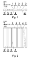
- Fig.1 and Fig.2 show accordingly a side and a top view of the first embodiment of a substrate according to the invention.
- Fig.3 and Fig.4 show accordingly a side and a top view of the second embodiment of the substrate according to the invention.
- Fig. 5 shows enlarged part of Fig. 4 .
- Fig.6 and Fig.7 show accordingly a side and a top view of a third embodiment of the substrate according to the invention.
- Fig. 8 and Fig.9 show a side and a top view of a laser diodes structure of non-absorbing mirrors fabricated on the substrate shown in Fig.1 and Fig.2 .
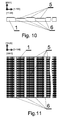
- Fig. 10 and Fig 11 show accordingly a side and a top view of a superluminescent diodes structure having a broadened optical spectrum.
- Fig.12 and Fig.13 show accordingly a side and a top view of a laser diode array emitting various wavelength and fabricated on the substrate shown in Fig.6 and Fig.7 .
- Substrate 1 for epitaxial growth was prepared from a monocrystalline gallium nitride forming a plane parallel platelet of the thickness of 120 ⁇ m.
- the gallium polar surface of the crystal was atomically flat after the mechanochemical polishing, showing atomic steps in the atomic force microscope image, and disorientation angle, defined as a angle between this surface and the crystallographic c direction of the hexagonal wurtzite structure defined by Bravais-Miller indices (0001), was 0.5 degree.
- disorientation angle defined as a angle between this surface and the crystallographic c direction of the hexagonal wurtzite structure defined by Bravais-Miller indices (0001), was 0.5 degree.
- the layer of the photosensitive emulsion of the thickness of 1.3 ⁇ m was span off.
- emulsion layer was exposed using a known laser photolithographic tool in such a way that various areas of this layer absorbed different doses of the radiation. These areas had the shapes of stripes having longer edges parallel one to the other and simultaneously parallel to the crystallographic direction having Miller-Bravais indices [11-20].
- the crystallographic direction defined by the indices is an easy cleavage direction of GaN crystal.
- the width of the exposed stripes was alternated between 670 ⁇ m and 30 ⁇ m.
- the energy emitted during the exposure of every stripe area was varied along the direction perpendicular to [11-20] direction and this variation was formed as a sequence of four steps. The first step of the sequence was an exposure of the 670 ⁇ m stripe over which the laser of the photolithographic tool was off.
- the second step of the sequence consisted in the linear increase of the laser illumination from zero to maximum laser radiation dose during the exposure of the 30 ⁇ m stripe (second stripe) adjoining the (un)exposed previous (first) stripe.
- the variation of the dose was performed in the direction perpendicular to the crystallographic direction [11-20] and was increased counting from the edge common with said previous stripe.
- the third step of the sequence consisted in the exposure of the entire next stripe (i.e. third 670 ⁇ m stripe) with the maximum dose of illumination.
- the sequence was completed with the fourth step during which next stripe of 30 ⁇ m was exposed with the linearly varying dose in the same direction as in case of the second stripe but in contrast to the second stripe the dose was being decreased from maximum to zero.
- the thickness of the emulsion became a function of the exposure dose meaning thinner when more heavily exposed. And so the emulsion thickness on the third stripe was zero while on the second and the fourth stripe the thickness was varying linearly from 1.3 ⁇ m to 0 ⁇ m and from 0 ⁇ m to 1.3 ⁇ m accordingly.
- the substrate with the layer of emulsion was subjected to Reactive Ion Etching in the mixture of Cl and Ar gases. During such process the etching medium attacks both the emulsion and the GaN crystal. In particular it is possible to find such parameters of the etching procedure that the etching rate of emulsion is almost equal to this of GaN.
- the time of etching was long enough to completely remove the emulsion in every of the four stripes areas in every stripe sequence.
- the variable profile of the emulsion thickness was reproduced in the GaN crystal as a sequence of flat surfaces having different angles of disorientation.
- the flat surfaces of the crystal located under the first and the third in the sequence emulsion stripes had the same disorientation angle (equal to the initial disorientation angle of the crystal i.e.; 0.5 degree) and they were called the first flat surfaces 2 of the substrate 1.
- the flat surfaces located under the second in the sequence emulsion stripes had the disorientation angle of 2.5 degree and they were called the second flat surfaces 3 of the substrate 1.
- the flat surfaces of the crystal located under the fourth in the sequence emulsion stripes had a disorientation angle of -1.5 degree and they were called the third flat surfaces 4 of the substrate 1.
- a laser diode structure MOVPE growth was conducted.
- the substrate 1 was placed in the MOVPE reactor where at the temperature about 1050°C the first Ga 0.92 Al 0.08 N layer was deposited. This layer had a thickness of 600 nm and was doped with Si to the level of 5 x 10 18 cm -3 .
- the layer of the undoped GaN of the thickness of 100 nm was grown and this layer played a role of lower waveguide.
- the reactor temperature was raised up to 1050°C and the Al 0,12 Ga 0,88 N:Mg electron blocking layer was grown. After that an undoped GaN layer forming the top waveguide was formed.
- a top Al 0,08 Ga 0,92 N cladding layer of a thickness of 350 nm was fabricated. The structure growth was completed with a thin GaN:Mg contact layer of the magnesium concentration higher than 10 20 cm -3 . After the completion of the growth the reactor was filled with nitrogen and cooled down.
- the top contact had a shape of a stripe of the length from a range of 300 to 2000 ⁇ m and the width from a range of 1 to 100 ⁇ m.
- the metal contact annealing was performed at the temperatures lower than 390°C.
- the laser may be equipped with the 300-450 nm ridge waveguide structure for better confinement of the electromagnetic mode. Thanks to the larger disorientation, within the second and the third flat surface the amount of incorporated indium is smaller than within the first flat surfaces ( Fig.7 and Fig.8 ). As a consequence the energy gap of the material building an active layer of a laser is larger within second and third flat surfaces than within the first flat surfaces.
- laser mirrors plates are (1-100) planes which goes through the centers of the second 3 and the third 4 flat surfaces and the electric contacts does not exceed its first flat surfaces 2. Thanks to this the laser radiation is emitted at the energy characteristic for the energy gap of the material within the first flat surfaces. The radiation passes by the areas of the second and third flat surfaces and reaches the laser mirrors. It is worth noting that the radiation emitted with the energy characteristic for the material of the first flat surfaces is not absorbed in the areas of the second and third flat surfaces and thus consequently the mirror optical damage known in conventional laser diodes does not occur in such a structure since the band gap of semiconductor in the areas of first flat surfaces is smaller than that in the areas of the second and third flat surfaces.
- the final laser structure is schematically shown in Fig. 8 and Fig.9 where the laser stripes were denoted with number 5 and the cleavage planes were denoted with number 6.
- a plane parallel platelet of gallium nitride has been prepared and covered with photosensitive emulsion as in the Example 1.
- successive emulsion stripes of the constant width were exposed with different doses.
- the stripe edges were parallel to the direction [11-20] of the gallium nitride crystal processed.
- One sequence of the changes of the laser exposure dose directed onto the emulsion consisted of 136 steps.
- the second and forth steps were unchanged.
- Previous first and third steps conducted on a width of 670 ⁇ m were replaced by two sequences of sixty seven steps conducted on width 10 ⁇ m.
- the emulsion thickness in the first group of sixty seven adjacent 10 ⁇ m width stripes was sequentially changed in the following four substeps: linear increase of thickness from 0 to 0.05 ⁇ m, constant thickness of 0.05 ⁇ m, linear decrease of thickness from 0.05 ⁇ m to 0 ⁇ m and no emulsion (thickness 0 ⁇ m).
- the second group of sixty seven 10 ⁇ m width stripes was sequentially changed in four substeps: linear decrease of thickness from 1.30 ⁇ m to 1.25 ⁇ m, constant thickness of 1.25 ⁇ m, linear increase of thickness from 1.25 ⁇ m to 1.30 ⁇ m and constant thickness of 1.30 ⁇ m.
- variable profile of the emulsion thickness was reproduced onto the GaN crystal.
- Flat surfaces located below the emulsion stripes of 10 ⁇ m width were named forth flat surfaces 7.
- Disorientation of four subsequent fourth flat surfaces 7 obtained as a result of realization of the four substeps described above on the first and second group of sixty seven 10 ⁇ m width stripes was as following ( Fig. 5 ): surface 7' - 0.5 degree, surface 7" - 0.2 degree, surface 7"' - 0.5 degree and surface 7"" - 0.8 degree.
- the planes of laser diode mirrors are planes of Miller indices (1-100) crosssectioning the centers of the second and third areas of the flat substrate surfaces while electrical contacts does not exceed the areas of the four flat surfaces. Thanks to that, the radiation is emitted in a wide spectral range characteristic for the variable energy gap of the material in area of the second flat surfaces.
- the prepared laser structure is shown in Fig. 10 and Fig.11 , where the laser stripes are denoted with number 5 and the cleavage plane - with number 6.
- a plane parallel platelet of gallium nitride has been prepared and covered with photosensitive emulsion as in the Example 1.
- the crystal surface covered with the emulsion had a disorientation by 0.5 degree with respect to the direction of crystallographic axis c ([0001]) of the hexagonal structure of GaN (wurtzite) onto a direction of [11-20].
- subsequent stripes of emulsion of the constant width were exposed with different doses.
- the stripe edges in this embodiment were parallel to the direction of [1-100] of the treated gallium nitride crystal.
- each sequence consisted of three adjacent flat surfaces: first (8, 9, 10 i 11), second (12, 13, 14 i 15) and third (16, 17, 18 i 19).
- Disorientation angle of all the first flat surfaces 8, 9, 10 and 11 was 0.5 degree due to presence of the photosensitive emulsion of a constant thickness of 1.3 ⁇ m in those areas. The disorientation angle in those areas did not change during the ion etching. Disorientation angles of other flat surfaces was obtained by using a linearly variable thickness of the photosensitive emulsion.
- the first flat surface 8 had a width of 100 ⁇ m
- the second flat surface 12 had a width of 100 ⁇ m and disorientation angle of 0.4 degrees
- the third flat surface 16 had a width of 100 ⁇ m and disorientation angle of 0.6 degrees.
- the second sequence consisted of the first flat surface 10 of 10 ⁇ m width, of the second flat surface 13 of 280 ⁇ m width and 0.7 degree disorientation angle, and of the third flat surface 17 of a 10 ⁇ m width and 5.5 degree disorientation angle.
- the third sequence consisted of the first flat surface 10 of 80 ⁇ m width, of a second flat surface 14 of 140 ⁇ m width and 0.9 degree disorientation angle, and of the third flat surface 18 of 80 ⁇ m width and 0.2 degree disorientation angle.
- the last sequence consisted of the first flat surface 11 of 110 ⁇ m width, of the second flat surface 15 of 80 ⁇ m width and 1.1 degree disorientation angle, and of the third flat surface 19 of 110 ⁇ m width and 0 degree disorientation angle.
- GaN substrate crystal was made epitaxial growth of laser diode structure in the same way as in the Example 1. Due to different disorientation in relation to axis c in areas of the individual flat surfaces different amounts of indium were incorporated. In this way, energy gap of the quantum wells forming laser active layer in the areas is different. The greater disorientation of given flat surface, the greater energy gap of semiconductor in its area.
- the laser stripes 5 were made in the middle of the second flat surfaces 8, 9, 10 and 11. Thanks to that, the laser radiation was realized with energies characteristic for the quantum well energy gaps within area of each second flat surfaces. Due to the different disorientation of said flat surfaces a monolithic arrays of four laser diodes, each emitting in different wavelengths, were obtained.
- the wavelengths were as following: 390 nm, 400 nm, 410 nm and 420 nm. Fabricating the laser structure on a substrate with bigger number of sequences of the three flat surfaces 3 will make it possible to obtain arrays of larger number of colours.
Landscapes
- Chemical & Material Sciences (AREA)
- Engineering & Computer Science (AREA)
- Physics & Mathematics (AREA)
- Crystallography & Structural Chemistry (AREA)
- Organic Chemistry (AREA)
- Materials Engineering (AREA)
- Metallurgy (AREA)
- Optics & Photonics (AREA)
- Nanotechnology (AREA)
- General Physics & Mathematics (AREA)
- Condensed Matter Physics & Semiconductors (AREA)
- Electromagnetism (AREA)
- Inorganic Chemistry (AREA)
- Life Sciences & Earth Sciences (AREA)
- Biophysics (AREA)
- Chemical Kinetics & Catalysis (AREA)
- General Chemical & Material Sciences (AREA)
- Plasma & Fusion (AREA)
- Semiconductor Lasers (AREA)
- Led Devices (AREA)
Description
- The subject of this invention is a substrate for epitaxial growth made of a gallium nitride crystal, having one surface prepared for the epitaxial growth as well as application of such substrate for fabrication of semiconductor light emitters.
- Since a long time the semiconductor structures have been fabricated using various epitaxial growth methods in which a substrate where the growth is initiated plays a one of key roles. A short-wavelength (360-530 nm) semiconductor light emitters such as electroluminescent diodes and laser diodes are usually fabricated in epitaxial growth on monocrystalline gallium nitride substrate. For preparing the substrate a gallium nitride crystal is treated for obtaining a substantially flat growth surface. An example method of GaN substrate preparation has been disclosed in
PL180448 EP 1806770 discloses a GaN substrate for epitaxial growth and having an epi-ready growth surface. This surface is provided with a set of neighbouring flat surfaces in the form of stripes having a width of e.g. 300-600 microns. These stripes are oriented according to a crystallographic direction. The purpose of the invention was to develop a new type of gallium nitride substrates for epitaxial growth enabling to obtain structures of semiconductor light emitters without the disadvantages described above. - A substrate according to the invention is characterized in that its growth surface consists of set of neighbouring flat surfaces in form of stripes of a width from 1 to 2000 µm. Longer edges of the stripes are parallel one to another and planes of the stripes are disoriented relatively to the crystallographic plane defined by Miller-Bravais indices (0001), (10-10), (11-22) or (11-20). Disorientation angle of each of the flat surfaces is from 0 to 3 degree and is different for each of two neighbouring surfaces.
- In one of variants of the substrate according to the invention all the flat surfaces are disoriented relatively to the crystallographic plane defined by the Miller-Bravais indices (0001).
- In another variant of the substrate according to the invention the longer edges of all the flat surfaces are parallel to a given crystallographic direction of gallium nitride crystal while the flat surfaces are delimited by said longer edges and form over the whole crystal an array of repeating sequences.
- In next variant of the substrate according to the invention the longer edges of all the flat surfaces are parallel to the crystallographic direction defined by Miller-Bravais indices [11-20].
- In next variant of the substrate according to the invention the repeating sequence constitute a set of four neighbouring, consecutively, a first, a second, a first and a third flat surfaces. The first flat surface has a width from 500 to 2000 µm and disorientation angle from 0.3 to 1 degree. Widths of the second and the third flat surface are from 5 to 100 µm. Disorientation angle of the second flat surface is larger than the disorientation angle of the first flat surface by 0.9 to 2 degree, and disorientation angle of the third flat surface is smaller than the disorientation angle of the first flat surface by 0.9 to 2 degrees.
- In next variant of the substrate according to the invention in the array of the flat surfaces forming repeating sequence in place of each first flat surface there are at least two fourth flat surfaces having a width of at least 10 µm each and disorientation angle amounting from 0.3 to 1 degree, whereby the total width of neighbouring the fourth flat surfaces is smaller than 2000 µm.
- In another variant of the substrate according to the invention the longer edges of all the flat surfaces are parallel to crystallographic direction defined by Miller-Bravais indices [1-100].
- In yet another variant of the substrate according to the invention all the flat surfaces are disoriented relatively to crystallographic plane (0001) in the direction [11-20], the repeating sequence of flat surfaces consists in an array of three neighbouring, consecutively., a first, a second and a third flat surfaces. The first flat surface has a width from 5 to 250 µm and a disorientation angle from 0.3 to 1 degree and constant over the whole area of gallium nitride crystal. Widths of the second and the third flat surfaces are from 5 to 290 µm. Disorientation angle of the second flat surface is larger than the disorientation angle of the first flat surface by 0.1 to 2 degrees. The disorientation angle of the third flat surface is smaller than the disorientation angle of the first flat surface by 0.1 to 2 degrees. The disorientation angles of each second and each third flat surface are different and the total number of all the second and the third flat surfaces does not exceed 200. Invention concerning application relies on application a substrate according to the invention for fabrication of a laser diode of non-absorbing mirrors emitting the light of the wavelength from 380 to 550 nm or fabrication of a laser diode array emitting simultaneously light of various wavelengths in the range of 380 to 550 nm, based on a layered structure AlInGaN obtained in epitaxial MOCVD or MBE growth on a GaN crystalline substrate.
- A method according to the invention relies on fabrication of a semiconductor light emitter, in particular a light emitting diode and a superluminescent diode having broadened emission spectrum, basing on a layered structure AlInGaN obtained in epitaxial MOCVD or MBE growth on the described above substrate according to the invention.
- It unexpectedly appeared that the substrate according to the invention allows for the effective control of the lateral composition of the active layer of a laser. Thereby it was possible to fabricate easily and economically new quantum structures based on InGaAlN emitting in UV, violet blue and green spectral region, which earlier were not possible to be realized within group III metal nitride material system. The invention allows also for easy fabrication of superluminescent diodes characterized by a broad optical gain and emission spectra as well as laser diode arrays emitting simultaneously at various wavelength as well as improvement of known laser structures i.e. fabrication of laser diodes of non-absorbing mirrors.
- The invention has been schematically shown in its embodiments in the attached drawing, on which
Fig.1 and Fig.2 show accordingly a side and a top view of the first embodiment of a substrate according to the invention.Fig.3 and Fig.4 . show accordingly a side and a top view of the second embodiment of the substrate according to the invention.Fig. 5 shows enlarged part ofFig. 4 .Fig.6 and Fig.7 show accordingly a side and a top view of a third embodiment of the substrate according to the invention.Fig. 8 and Fig.9 show a side and a top view of a laser diodes structure of non-absorbing mirrors fabricated on the substrate shown inFig.1 and Fig.2 .Fig. 10 and Fig 11 show accordingly a side and a top view of a superluminescent diodes structure having a broadened optical spectrum.Fig.12 and Fig.13 show accordingly a side and a top view of a laser diode array emitting various wavelength and fabricated on the substrate shown inFig.6 and Fig.7 . - This invention will be explained basing on three below exemplary embodiments. On each figure arrows show three basic crystallographic directions of the GaN crystal used for making the substrate.
-
Substrate 1 for epitaxial growth was prepared from a monocrystalline gallium nitride forming a plane parallel platelet of the thickness of 120 µm. The gallium polar surface of the crystal was atomically flat after the mechanochemical polishing, showing atomic steps in the atomic force microscope image, and disorientation angle, defined as a angle between this surface and the crystallographic c direction of the hexagonal wurtzite structure defined by Bravais-Miller indices (0001), was 0.5 degree. Over so prepared surface the layer of the photosensitive emulsion of the thickness of 1.3 µm was span off. Then emulsion layer was exposed using a known laser photolithographic tool in such a way that various areas of this layer absorbed different doses of the radiation. These areas had the shapes of stripes having longer edges parallel one to the other and simultaneously parallel to the crystallographic direction having Miller-Bravais indices [11-20]. The crystallographic direction defined by the indices is an easy cleavage direction of GaN crystal. The width of the exposed stripes was alternated between 670 µm and 30 µm. The energy emitted during the exposure of every stripe area was varied along the direction perpendicular to [11-20] direction and this variation was formed as a sequence of four steps. The first step of the sequence was an exposure of the 670 µm stripe over which the laser of the photolithographic tool was off. The second step of the sequence consisted in the linear increase of the laser illumination from zero to maximum laser radiation dose during the exposure of the 30 µm stripe (second stripe) adjoining the (un)exposed previous (first) stripe. The variation of the dose was performed in the direction perpendicular to the crystallographic direction [11-20] and was increased counting from the edge common with said previous stripe. The third step of the sequence consisted in the exposure of the entire next stripe (i.e. third 670 µm stripe) with the maximum dose of illumination. The sequence was completed with the fourth step during which next stripe of 30 µm was exposed with the linearly varying dose in the same direction as in case of the second stripe but in contrast to the second stripe the dose was being decreased from maximum to zero. After the chemical developing, the thickness of the emulsion became a function of the exposure dose meaning thinner when more heavily exposed. And so the emulsion thickness on the third stripe was zero while on the second and the fourth stripe the thickness was varying linearly from 1.3 µm to 0 µm and from 0 µm to 1.3 µm accordingly. In next step the substrate with the layer of emulsion was subjected to Reactive Ion Etching in the mixture of Cl and Ar gases. During such process the etching medium attacks both the emulsion and the GaN crystal. In particular it is possible to find such parameters of the etching procedure that the etching rate of emulsion is almost equal to this of GaN. The time of etching was long enough to completely remove the emulsion in every of the four stripes areas in every stripe sequence. In such a way the variable profile of the emulsion thickness was reproduced in the GaN crystal as a sequence of flat surfaces having different angles of disorientation. In this embodiment the flat surfaces of the crystal located under the first and the third in the sequence emulsion stripes had the same disorientation angle (equal to the initial disorientation angle of the crystal i.e.; 0.5 degree) and they were called the firstflat surfaces 2 of thesubstrate 1. The flat surfaces located under the second in the sequence emulsion stripes had the disorientation angle of 2.5 degree and they were called the secondflat surfaces 3 of thesubstrate 1. Analogically, the flat surfaces of the crystal located under the fourth in the sequence emulsion stripes had a disorientation angle of -1.5 degree and they were called the thirdflat surfaces 4 of thesubstrate 1. On such prepared GaN crystal substrate (Fig.1, Fig.2 ) was conducted a laser diode structure MOVPE growth. Thesubstrate 1 was placed in the MOVPE reactor where at the temperature about 1050°C the first Ga0.92Al0.08N layer was deposited. This layer had a thickness of 600 nm and was doped with Si to the level of 5 x 1018cm-3. Next, at the same temperature, the layer of the undoped GaN of the thickness of 100 nm was grown and this layer played a role of lower waveguide. After lowering the growth temperature down to 820°C the In0,1Ga0,9N/In0,01Ga0,99N multi quantum layer was deposited and the number of repetition was three. Next, the reactor temperature was raised up to 1050°C and the Al0,12Ga0,88N:Mg electron blocking layer was grown. After that an undoped GaN layer forming the top waveguide was formed. As a next layer, a top Al0,08Ga0,92N cladding layer of a thickness of 350 nm was fabricated. The structure growth was completed with a thin GaN:Mg contact layer of the magnesium concentration higher than 1020cm-3. After the completion of the growth the reactor was filled with nitrogen and cooled down. Next on the surfaces of the laser diode structure n- and p-type contacts were deposited. The top contact had a shape of a stripe of the length from a range of 300 to 2000 µm and the width from a range of 1 to 100 µm. The metal contact annealing was performed at the temperatures lower than 390°C. The laser may be equipped with the 300-450 nm ridge waveguide structure for better confinement of the electromagnetic mode. Thanks to the larger disorientation, within the second and the third flat surface the amount of incorporated indium is smaller than within the first flat surfaces (Fig.7 andFig.8 ). As a consequence the energy gap of the material building an active layer of a laser is larger within second and third flat surfaces than within the first flat surfaces. In this embodiment laser mirrors plates are (1-100) planes which goes through the centers of the second 3 and the third 4 flat surfaces and the electric contacts does not exceed its firstflat surfaces 2. Thanks to this the laser radiation is emitted at the energy characteristic for the energy gap of the material within the first flat surfaces. The radiation passes by the areas of the second and third flat surfaces and reaches the laser mirrors. It is worth noting that the radiation emitted with the energy characteristic for the material of the first flat surfaces is not absorbed in the areas of the second and third flat surfaces and thus consequently the mirror optical damage known in conventional laser diodes does not occur in such a structure since the band gap of semiconductor in the areas of first flat surfaces is smaller than that in the areas of the second and third flat surfaces. The final laser structure is schematically shown inFig. 8 and Fig.9 where the laser stripes were denoted withnumber 5 and the cleavage planes were denoted withnumber 6. - A plane parallel platelet of gallium nitride has been prepared and covered with photosensitive emulsion as in the Example 1. Similarly to the Example 1, using the laser photolithography tool successive emulsion stripes of the constant width were exposed with different doses. The stripe edges were parallel to the direction [11-20] of the gallium nitride crystal processed. One sequence of the changes of the laser exposure dose directed onto the emulsion consisted of 136 steps. With respect to the sequence of the Example 1, the second and forth steps were unchanged. Previous first and third steps conducted on a width of 670 µm were replaced by two sequences of sixty seven steps conducted on
width 10 µm. The emulsion thickness in the first group of sixty seven adjacent 10 µm width stripes was sequentially changed in the following four substeps: linear increase of thickness from 0 to 0.05 µm, constant thickness of 0.05 µm, linear decrease of thickness from 0.05 µm to 0 µm and no emulsion (thickness 0 µm). In the second group of sixty seven 10 µm width stripes was sequentially changed in four substeps: linear decrease of thickness from 1.30 µm to 1.25 µm, constant thickness of 1.25 µm, linear increase of thickness from 1.25 µm to 1.30 µm and constant thickness of 1.30 µm. As a result of ion etching similar to that of the Example 1, variable profile of the emulsion thickness was reproduced onto the GaN crystal. Flat surfaces located below the emulsion stripes of 10 µm width were named forthflat surfaces 7. Disorientation of four subsequent fourthflat surfaces 7 obtained as a result of realization of the four substeps described above on the first and second group of sixty seven 10 µm width stripes was as following (Fig. 5 ): surface 7' - 0.5 degree,surface 7" - 0.2 degree,surface 7"' - 0.5 degree andsurface 7"" - 0.8 degree. Disorientation angles of the secondflat surfaces 3 amounted to 2.5 degrees and disorientation angles of the thirdflat surfaces 4 amounted to 1.5 degree. On such prepared GaN substrate crystal (Fig.3 andFig. 5 ) was made MOVPE epitaxial growth of laser diode in the same way as in the Example 1. Due to variable disorientation on the areas of the fourth flat surfaces a variable amount of indium was incorporated in the structure. In this way, energy gap of the quantum wells in the area of the second flat surfaces was variable. Such system had a capability of radiation emission in a much wider spectral range compared to the system of uniform disorientation and indium content in the quantum wells. Thanks to a larger disorientation, in the area of the second and third flat surfaces, less indium was incorporated as compared to the forth flat surfaces. Thanks to that, it was possible to avoid a harmful radiation absorption, what was described more precisely in the first Example. In this embodiment, the planes of laser diode mirrors are planes of Miller indices (1-100) crosssectioning the centers of the second and third areas of the flat substrate surfaces while electrical contacts does not exceed the areas of the four flat surfaces. Thanks to that, the radiation is emitted in a wide spectral range characteristic for the variable energy gap of the material in area of the second flat surfaces. The prepared laser structure is shown inFig. 10 and Fig.11 , where the laser stripes are denoted withnumber 5 and the cleavage plane - withnumber 6. - A plane parallel platelet of gallium nitride has been prepared and covered with photosensitive emulsion as in the Example 1. The crystal surface covered with the emulsion had a disorientation by 0.5 degree with respect to the direction of crystallographic axis c ([0001]) of the hexagonal structure of GaN (wurtzite) onto a direction of [11-20]. Similarly to the Example 1, using the laser photolithographic tool subsequent stripes of emulsion of the constant width were exposed with different doses. The stripe edges in this embodiment were parallel to the direction of [1-100] of the treated gallium nitride crystal. Similarly to the Example 1, using the ion etching, four sequences of disoriented flat surfaces in form of stripes of variable width were obtained (
Fig.6 and Fig.7 ). Each sequence consisted of three adjacent flat surfaces: first (8, 9, 10 i 11), second (12, 13, 14 i 15) and third (16, 17, 18 i 19). Disorientation angle of all the firstflat surfaces flat surface 8 had a width of 100 µm, the secondflat surface 12 had a width of 100 µm and disorientation angle of 0.4 degrees, and the thirdflat surface 16 had a width of 100 µm and disorientation angle of 0.6 degrees. - The second sequence consisted of the first
flat surface 10 of 10 µm width, of the secondflat surface 13 of 280 µm width and 0.7 degree disorientation angle, and of the thirdflat surface 17 of a 10 µm width and 5.5 degree disorientation angle. The third sequence consisted of the firstflat surface 10 of 80 µm width, of a secondflat surface 14 of 140 µm width and 0.9 degree disorientation angle, and of the thirdflat surface 18 of 80 µm width and 0.2 degree disorientation angle. The last sequence consisted of the firstflat surface 11 of 110 µm width, of the secondflat surface 15 of 80 µm width and 1.1 degree disorientation angle, and of the thirdflat surface 19 of 110 µm width and 0 degree disorientation angle. On such prepared GaN substrate crystal was made epitaxial growth of laser diode structure in the same way as in the Example 1. Due to different disorientation in relation to axis c in areas of the individual flat surfaces different amounts of indium were incorporated. In this way, energy gap of the quantum wells forming laser active layer in the areas is different. The greater disorientation of given flat surface, the greater energy gap of semiconductor in its area. In this embodiment, thelaser stripes 5 were made in the middle of the secondflat surfaces flat surfaces 3 will make it possible to obtain arrays of larger number of colours.
Claims (11)
- A substrate for epitaxial growth made of gallium nitride crystal, and having epi-ready growth surface, characterized in that the growth surface consists of set of neighbouring flat surfaces in form of stripes of a width from 1 to 2000 µm, longer edges of the stripes are parallel on to another, planes of the stripes are disoriented relatively to the crystallographic plane defined by Miller-Bravais indices (0001), (10-10), (11-22) or (11-20) and disorientation angle of each of the flat surfaces is from 0 to 3 degree and it is different for each of two neighbouring surfaces.
- The substrate according to Claim 1, further
characterized in that all the flat surfaces are disoriented relatively to the crystallographic plane defined by the Miller-Bravais indices (0001). - The substrate according to Claim 2, further
characterized in that the longer edges of all the flat surfaces are parallel to a given crystallographic direction of gallium nitride crystal while the flat surfaces are delimited by said longer edges and form over the whole crystal an array of repeating sequences. - The substrate according to Claim 3, further
characterized in that the longer edges of all the flat surfaces are parallel to the crystallographic direction defined by Miller-Bravais indices [11-20]. - The substrate according to Claim 4, further
characterized in that the repeating sequence constitute a set of four neighbouring, consecutively, a first, a second, a first and a third flat surfaces, whereby the first flat surface has a width from 500 to 2000 µm and disorientation angle from 0.3 to 1 degree, widths of the second and the third flat surface are from 5 to 100 µm, disorientation angle of the second flat surface is larger than the disorientation angle of the first flat surface by 0.9 to 2 degree, and disorientation angle of the third flat surface is smaller than the disorientation angle of the first flat surface by 0.9 to 2 degrees. - The substrate according to Claim 5, further
characterized in that in the array of the flat surfaces forming repeating sequence in place of each first flat surface there are at least two fourth flat surfaces having a width of at least 10 µm each and disorientation angle amounting to from 0.3 to 1 degree, whereby the total width of neighbouring the fourth flat surfaces is smaller than 2000 µm. - The substrate according to Claim 2, further
characterized in that the longer edges of all the flat surfaces are parallel to crystallographic direction defined by Miller-Bravais indices [1-100]. - The substrate according to Claim 7, further
characterized in that all the flat surfaces are disoriented relatively to crystallographic plane (0001) in the direction [11-20], the repeating sequence of flat surfaces consists in an array of three neighbouring, consecutively, a first, a second and a third flat surfaces, whereby the first flat surface has a width from 5 to 250 µm and a disorientation angle from 0.3 to 1 degree and constant over the whole area of gallium nitride crystal, widths of the second and the third flat surfaces are from 5 to 290 µm, disorientation angle of the second flat surface is larger than the disorientation angle of the first flat surface by 0.1 to 2 degrees, the disorientation angle of the third flat surface is smaller than the disorientation angle of the first flat surface by 0.1 to 2 degrees, while the disorientation angles of each second and each third flat surface are different and the total number of all the second and the third flat surfaces does not exceed 200. - Application of a substrate made of crystalline gallium nitride and having a growth surface according to one of Claims 1 to 8 for fabrication of a laser diode of non-absorbing mirrors emitting the light of the wavelength from 380 to 550 nm based on a layered structure AlInGaN obtained in epitaxial MOCVD or MBE growth on a GaN crystalline substrate.
- Application of a substrate made of crystalline gallium nitride and having a growth surface according to one of Claims 1 to 8 for fabrication a laser diode array emitting simultaneously light of various wavelengths in the range of 380 to 550 nm based on a layered structure AlInGaN obtained in epitaxial MOCVD or MBE growth on a crystalline GaN substrate.
- A method of fabrication a semiconductor light emitter, in particular a light emitting diode and a superluminescent diode having broadened emission spectrum, based on a layered structure AlInGaN obtained in epitaxial MOCVD or MBE growth on a crystalline substrate made of gallium nitride, characterized in that the epitaxial growth of said layered structure is performed on a substrate according one of Claims 1 to 8.
Priority Applications (1)
| Application Number | Priority Date | Filing Date | Title |
|---|---|---|---|
| PL11717334T PL2567004T3 (en) | 2010-04-06 | 2011-03-15 | Medium for epitaxial growth |
Applications Claiming Priority (2)
| Application Number | Priority Date | Filing Date | Title |
|---|---|---|---|
| PL390926A PL224995B1 (en) | 2010-04-06 | 2010-04-06 | Substrate for epitaxial growth |
| PCT/IB2011/051091 WO2011124997A1 (en) | 2010-04-06 | 2011-03-15 | Substrate for epitaxial growth |
Publications (2)
| Publication Number | Publication Date |
|---|---|
| EP2567004A1 EP2567004A1 (en) | 2013-03-13 |
| EP2567004B1 true EP2567004B1 (en) | 2015-03-04 |
Family
ID=44148764
Family Applications (1)
| Application Number | Title | Priority Date | Filing Date |
|---|---|---|---|
| EP20110717334 Active EP2567004B1 (en) | 2010-04-06 | 2011-03-15 | Substrate for epitaxial growth |
Country Status (4)
| Country | Link |
|---|---|
| US (1) | US8975639B2 (en) |
| EP (1) | EP2567004B1 (en) |
| PL (2) | PL224995B1 (en) |
| WO (1) | WO2011124997A1 (en) |
Cited By (1)
| Publication number | Priority date | Publication date | Assignee | Title |
|---|---|---|---|---|
| WO2023096514A1 (en) | 2021-11-26 | 2023-06-01 | Topgan Sp. Z O.O. | Laser and light guide system and manufacturing method thereof |
Families Citing this family (2)
| Publication number | Priority date | Publication date | Assignee | Title |
|---|---|---|---|---|
| PL228006B1 (en) | 2015-09-23 | 2018-02-28 | Inst Wysokich Ciśnień Polskiej Akademii Nauk | AlInGaN-based superluminescent diode |
| PL238875B1 (en) * | 2018-03-09 | 2021-10-18 | Instytut Tech Elektronowej | Method for making through hole in complex semiconductor structure and the complex semiconductor structure |
Family Cites Families (13)
| Publication number | Priority date | Publication date | Assignee | Title |
|---|---|---|---|---|
| GB240770A (en) | 1925-06-22 | 1925-10-08 | Julia Hill | Improved stabilising device for cycle-trailer combinations |
| PL173917B1 (en) * | 1993-08-10 | 1998-05-29 | Ct Badan Wysokocisnieniowych P | Method of obtaining a crystalline lamellar structure |
| JP3656454B2 (en) | 1999-04-01 | 2005-06-08 | 日亜化学工業株式会社 | Nitride semiconductor laser device |
| JP3929008B2 (en) * | 2000-01-14 | 2007-06-13 | シャープ株式会社 | Nitride-based compound semiconductor light-emitting device and method for manufacturing the same |
| ATE445722T1 (en) | 2002-12-11 | 2009-10-15 | Ammono Sp Zoo | STENCIL-LIKE SUBSTRATE AND METHOD FOR PRODUCING IT |
| US7118813B2 (en) * | 2003-11-14 | 2006-10-10 | Cree, Inc. | Vicinal gallium nitride substrate for high quality homoepitaxy |
| JP3888374B2 (en) | 2004-03-17 | 2007-02-28 | 住友電気工業株式会社 | Manufacturing method of GaN single crystal substrate |
| US20050218414A1 (en) | 2004-03-30 | 2005-10-06 | Tetsuzo Ueda | 4H-polytype gallium nitride-based semiconductor device on a 4H-polytype substrate |
| KR100848380B1 (en) | 2004-06-11 | 2008-07-25 | 암모노 에스피. 제트오. 오. | Bulk single crystal of gallium-containing nitride and its application |
| PL368781A1 (en) | 2004-06-25 | 2005-12-27 | Ammono Sp.Z O.O. | Gallium containing nitride monocrystal and its application |
| PL368483A1 (en) | 2004-06-11 | 2005-12-12 | Ammono Sp.Z O.O. | Monocrystals of nitride containing gallium and its application |
| CN1977359A (en) | 2005-07-21 | 2007-06-06 | 住友电气工业株式会社 | Gallium nitride wafer |
| EP2003230A2 (en) | 2007-06-14 | 2008-12-17 | Sumitomo Electric Industries, Ltd. | GaN substrate, substrate with an epitaxial layer, semiconductor device, and GaN substrate manufacturing method |
-
2010
- 2010-04-06 PL PL390926A patent/PL224995B1/en unknown
-
2011
- 2011-03-15 EP EP20110717334 patent/EP2567004B1/en active Active
- 2011-03-15 US US13/639,907 patent/US8975639B2/en active Active
- 2011-03-15 PL PL11717334T patent/PL2567004T3/en unknown
- 2011-03-15 WO PCT/IB2011/051091 patent/WO2011124997A1/en not_active Ceased
Cited By (1)
| Publication number | Priority date | Publication date | Assignee | Title |
|---|---|---|---|---|
| WO2023096514A1 (en) | 2021-11-26 | 2023-06-01 | Topgan Sp. Z O.O. | Laser and light guide system and manufacturing method thereof |
Also Published As
| Publication number | Publication date |
|---|---|
| US8975639B2 (en) | 2015-03-10 |
| PL390926A1 (en) | 2011-10-10 |
| US20130099246A1 (en) | 2013-04-25 |
| PL2567004T3 (en) | 2015-12-31 |
| EP2567004A1 (en) | 2013-03-13 |
| PL224995B1 (en) | 2017-02-28 |
| WO2011124997A1 (en) | 2011-10-13 |
Similar Documents
| Publication | Publication Date | Title |
|---|---|---|
| US7408199B2 (en) | Nitride semiconductor laser device and nitride semiconductor device | |
| JP4786691B2 (en) | Semiconductor device and manufacturing method thereof | |
| US6606335B1 (en) | Semiconductor laser, semiconductor device, and their manufacture methods | |
| EP0852416B1 (en) | Semiconductor material, method of producing the semiconductor material, and semiconductor device | |
| EP1104031B1 (en) | Nitride semiconductor laser diode and method of fabricating the same | |
| KR100917260B1 (en) | Crystal Films, Crystal Substrates, and Semiconductor Devices | |
| EP1496584B1 (en) | Nitride semiconductor laser device and method of manufacturing the nitride semiconductor laser device | |
| KR20030007907A (en) | Semiconductor laser device, and method of manufacturing the same | |
| US20060060833A1 (en) | Radiation-emitting optoelectronic component with a quantum well structure and method for producing it | |
| JP5076656B2 (en) | Nitride semiconductor laser device | |
| JPH11135770A (en) | Iii-v compd. semiconductor, manufacture thereof and semiconductor element | |
| KR20010076264A (en) | Semiconductor device | |
| JP2009094360A (en) | Semiconductor laser diode | |
| US20100259184A1 (en) | Light-emitting device | |
| DE102017108435A1 (en) | Semiconductor laser diode and method for producing a semiconductor laser diode | |
| JP4822608B2 (en) | Nitride-based semiconductor light-emitting device and manufacturing method thereof | |
| US8975639B2 (en) | Substrate for epitaxial growth | |
| JP2004179350A (en) | Nitride semiconductor laser device and method of manufacturing the same | |
| JP2008028375A (en) | Nitride semiconductor laser device | |
| JP3562478B2 (en) | Method for growing nitride semiconductor and device using the same | |
| JP4104234B2 (en) | Semiconductor light emitting device and manufacturing method thereof | |
| JP5532082B2 (en) | Nitride semiconductor laser device | |
| RU2262171C2 (en) | Semiconductor laser unit and its manufacturing process | |
| KR200318416Y1 (en) | Nitride Semiconductor Laser Device | |
| JP2007201379A (en) | Compound semiconductor substrate, its manufacturing method, and semiconductor device |
Legal Events
| Date | Code | Title | Description |
|---|---|---|---|
| PUAI | Public reference made under article 153(3) epc to a published international application that has entered the european phase |
Free format text: ORIGINAL CODE: 0009012 |
|
| 17P | Request for examination filed |
Effective date: 20121103 |
|
| AK | Designated contracting states |
Kind code of ref document: A1 Designated state(s): AL AT BE BG CH CY CZ DE DK EE ES FI FR GB GR HR HU IE IS IT LI LT LU LV MC MK MT NL NO PL PT RO RS SE SI SK SM TR |
|
| DAX | Request for extension of the european patent (deleted) | ||
| GRAP | Despatch of communication of intention to grant a patent |
Free format text: ORIGINAL CODE: EPIDOSNIGR1 |
|
| RIC1 | Information provided on ipc code assigned before grant |
Ipc: H01L 21/02 20060101ALI20140815BHEP Ipc: C30B 25/18 20060101AFI20140815BHEP Ipc: H01S 5/343 20060101ALI20140815BHEP Ipc: C30B 29/40 20060101ALI20140815BHEP Ipc: H01S 5/40 20060101ALI20140815BHEP Ipc: H01L 21/20 20060101ALI20140815BHEP Ipc: C30B 33/00 20060101ALI20140815BHEP Ipc: H01S 5/20 20060101ALI20140815BHEP Ipc: H01S 5/34 20060101ALI20140815BHEP Ipc: H01S 5/32 20060101ALI20140815BHEP Ipc: H01L 29/20 20060101ALI20140815BHEP Ipc: H01S 5/02 20060101ALI20140815BHEP Ipc: B82Y 20/00 20110101ALI20140815BHEP Ipc: H01L 33/00 20100101ALI20140815BHEP Ipc: C30B 33/12 20060101ALI20140815BHEP |
|
| INTG | Intention to grant announced |
Effective date: 20140912 |
|
| GRAS | Grant fee paid |
Free format text: ORIGINAL CODE: EPIDOSNIGR3 |
|
| GRAA | (expected) grant |
Free format text: ORIGINAL CODE: 0009210 |
|
| RIN1 | Information on inventor provided before grant (corrected) |
Inventor name: SARZYNSKI, MARCIN Inventor name: SUSKI, TADEUSZ Inventor name: CZERNECKI, ROBERT Inventor name: LESZCZYNSKI, MICHAL Inventor name: PERLIN, PIOTR |
|
| AK | Designated contracting states |
Kind code of ref document: B1 Designated state(s): AL AT BE BG CH CY CZ DE DK EE ES FI FR GB GR HR HU IE IS IT LI LT LU LV MC MK MT NL NO PL PT RO RS SE SI SK SM TR |
|
| REG | Reference to a national code |
Ref country code: GB Ref legal event code: FG4D |
|
| REG | Reference to a national code |
Ref country code: CH Ref legal event code: EP |
|
| REG | Reference to a national code |
Ref country code: IE Ref legal event code: FG4D |
|
| REG | Reference to a national code |
Ref country code: AT Ref legal event code: REF Ref document number: 713995 Country of ref document: AT Kind code of ref document: T Effective date: 20150415 |
|
| REG | Reference to a national code |
Ref country code: DE Ref legal event code: R096 Ref document number: 602011014324 Country of ref document: DE Effective date: 20150416 |
|
| REG | Reference to a national code |
Ref country code: FR Ref legal event code: PLFP Year of fee payment: 5 |
|
| REG | Reference to a national code |
Ref country code: AT Ref legal event code: MK05 Ref document number: 713995 Country of ref document: AT Kind code of ref document: T Effective date: 20150304 Ref country code: NL Ref legal event code: VDEP Effective date: 20150304 |
|
| PG25 | Lapsed in a contracting state [announced via postgrant information from national office to epo] |
Ref country code: FI Free format text: LAPSE BECAUSE OF FAILURE TO SUBMIT A TRANSLATION OF THE DESCRIPTION OR TO PAY THE FEE WITHIN THE PRESCRIBED TIME-LIMIT Effective date: 20150304 Ref country code: SE Free format text: LAPSE BECAUSE OF FAILURE TO SUBMIT A TRANSLATION OF THE DESCRIPTION OR TO PAY THE FEE WITHIN THE PRESCRIBED TIME-LIMIT Effective date: 20150304 Ref country code: LT Free format text: LAPSE BECAUSE OF FAILURE TO SUBMIT A TRANSLATION OF THE DESCRIPTION OR TO PAY THE FEE WITHIN THE PRESCRIBED TIME-LIMIT Effective date: 20150304 Ref country code: HR Free format text: LAPSE BECAUSE OF FAILURE TO SUBMIT A TRANSLATION OF THE DESCRIPTION OR TO PAY THE FEE WITHIN THE PRESCRIBED TIME-LIMIT Effective date: 20150304 Ref country code: ES Free format text: LAPSE BECAUSE OF FAILURE TO SUBMIT A TRANSLATION OF THE DESCRIPTION OR TO PAY THE FEE WITHIN THE PRESCRIBED TIME-LIMIT Effective date: 20150304 Ref country code: NO Free format text: LAPSE BECAUSE OF FAILURE TO SUBMIT A TRANSLATION OF THE DESCRIPTION OR TO PAY THE FEE WITHIN THE PRESCRIBED TIME-LIMIT Effective date: 20150604 |
|
| REG | Reference to a national code |
Ref country code: LT Ref legal event code: MG4D |
|
| PG25 | Lapsed in a contracting state [announced via postgrant information from national office to epo] |
Ref country code: RS Free format text: LAPSE BECAUSE OF FAILURE TO SUBMIT A TRANSLATION OF THE DESCRIPTION OR TO PAY THE FEE WITHIN THE PRESCRIBED TIME-LIMIT Effective date: 20150304 Ref country code: LV Free format text: LAPSE BECAUSE OF FAILURE TO SUBMIT A TRANSLATION OF THE DESCRIPTION OR TO PAY THE FEE WITHIN THE PRESCRIBED TIME-LIMIT Effective date: 20150304 Ref country code: GR Free format text: LAPSE BECAUSE OF FAILURE TO SUBMIT A TRANSLATION OF THE DESCRIPTION OR TO PAY THE FEE WITHIN THE PRESCRIBED TIME-LIMIT Effective date: 20150605 Ref country code: AT Free format text: LAPSE BECAUSE OF FAILURE TO SUBMIT A TRANSLATION OF THE DESCRIPTION OR TO PAY THE FEE WITHIN THE PRESCRIBED TIME-LIMIT Effective date: 20150304 |
|
| PG25 | Lapsed in a contracting state [announced via postgrant information from national office to epo] |
Ref country code: NL Free format text: LAPSE BECAUSE OF FAILURE TO SUBMIT A TRANSLATION OF THE DESCRIPTION OR TO PAY THE FEE WITHIN THE PRESCRIBED TIME-LIMIT Effective date: 20150304 |
|
| PG25 | Lapsed in a contracting state [announced via postgrant information from national office to epo] |
Ref country code: RO Free format text: LAPSE BECAUSE OF FAILURE TO SUBMIT A TRANSLATION OF THE DESCRIPTION OR TO PAY THE FEE WITHIN THE PRESCRIBED TIME-LIMIT Effective date: 20150304 Ref country code: SK Free format text: LAPSE BECAUSE OF FAILURE TO SUBMIT A TRANSLATION OF THE DESCRIPTION OR TO PAY THE FEE WITHIN THE PRESCRIBED TIME-LIMIT Effective date: 20150304 Ref country code: PT Free format text: LAPSE BECAUSE OF FAILURE TO SUBMIT A TRANSLATION OF THE DESCRIPTION OR TO PAY THE FEE WITHIN THE PRESCRIBED TIME-LIMIT Effective date: 20150706 Ref country code: EE Free format text: LAPSE BECAUSE OF FAILURE TO SUBMIT A TRANSLATION OF THE DESCRIPTION OR TO PAY THE FEE WITHIN THE PRESCRIBED TIME-LIMIT Effective date: 20150304 Ref country code: CZ Free format text: LAPSE BECAUSE OF FAILURE TO SUBMIT A TRANSLATION OF THE DESCRIPTION OR TO PAY THE FEE WITHIN THE PRESCRIBED TIME-LIMIT Effective date: 20150304 |
|
| REG | Reference to a national code |
Ref country code: CH Ref legal event code: PL |
|
| PG25 | Lapsed in a contracting state [announced via postgrant information from national office to epo] |
Ref country code: IS Free format text: LAPSE BECAUSE OF FAILURE TO SUBMIT A TRANSLATION OF THE DESCRIPTION OR TO PAY THE FEE WITHIN THE PRESCRIBED TIME-LIMIT Effective date: 20150704 |
|
| REG | Reference to a national code |
Ref country code: DE Ref legal event code: R097 Ref document number: 602011014324 Country of ref document: DE |
|
| PG25 | Lapsed in a contracting state [announced via postgrant information from national office to epo] |
Ref country code: IT Free format text: LAPSE BECAUSE OF FAILURE TO SUBMIT A TRANSLATION OF THE DESCRIPTION OR TO PAY THE FEE WITHIN THE PRESCRIBED TIME-LIMIT Effective date: 20150304 |
|
| REG | Reference to a national code |
Ref country code: PL Ref legal event code: T3 |
|
| PLBE | No opposition filed within time limit |
Free format text: ORIGINAL CODE: 0009261 |
|
| STAA | Information on the status of an ep patent application or granted ep patent |
Free format text: STATUS: NO OPPOSITION FILED WITHIN TIME LIMIT |
|
| REG | Reference to a national code |
Ref country code: IE Ref legal event code: MM4A |
|
| PG25 | Lapsed in a contracting state [announced via postgrant information from national office to epo] |
Ref country code: CH Free format text: LAPSE BECAUSE OF NON-PAYMENT OF DUE FEES Effective date: 20150331 Ref country code: DK Free format text: LAPSE BECAUSE OF FAILURE TO SUBMIT A TRANSLATION OF THE DESCRIPTION OR TO PAY THE FEE WITHIN THE PRESCRIBED TIME-LIMIT Effective date: 20150304 Ref country code: LI Free format text: LAPSE BECAUSE OF NON-PAYMENT OF DUE FEES Effective date: 20150331 Ref country code: MC Free format text: LAPSE BECAUSE OF FAILURE TO SUBMIT A TRANSLATION OF THE DESCRIPTION OR TO PAY THE FEE WITHIN THE PRESCRIBED TIME-LIMIT Effective date: 20150304 Ref country code: IE Free format text: LAPSE BECAUSE OF NON-PAYMENT OF DUE FEES Effective date: 20150315 |
|
| 26N | No opposition filed |
Effective date: 20151207 |
|
| PG25 | Lapsed in a contracting state [announced via postgrant information from national office to epo] |
Ref country code: SI Free format text: LAPSE BECAUSE OF FAILURE TO SUBMIT A TRANSLATION OF THE DESCRIPTION OR TO PAY THE FEE WITHIN THE PRESCRIBED TIME-LIMIT Effective date: 20150304 |
|
| REG | Reference to a national code |
Ref country code: FR Ref legal event code: PLFP Year of fee payment: 6 |
|
| PG25 | Lapsed in a contracting state [announced via postgrant information from national office to epo] |
Ref country code: BE Free format text: LAPSE BECAUSE OF FAILURE TO SUBMIT A TRANSLATION OF THE DESCRIPTION OR TO PAY THE FEE WITHIN THE PRESCRIBED TIME-LIMIT Effective date: 20150304 |
|
| PG25 | Lapsed in a contracting state [announced via postgrant information from national office to epo] |
Ref country code: MT Free format text: LAPSE BECAUSE OF FAILURE TO SUBMIT A TRANSLATION OF THE DESCRIPTION OR TO PAY THE FEE WITHIN THE PRESCRIBED TIME-LIMIT Effective date: 20150304 |
|
| REG | Reference to a national code |
Ref country code: FR Ref legal event code: PLFP Year of fee payment: 7 |
|
| PG25 | Lapsed in a contracting state [announced via postgrant information from national office to epo] |
Ref country code: HU Free format text: LAPSE BECAUSE OF FAILURE TO SUBMIT A TRANSLATION OF THE DESCRIPTION OR TO PAY THE FEE WITHIN THE PRESCRIBED TIME-LIMIT; INVALID AB INITIO Effective date: 20110315 Ref country code: BG Free format text: LAPSE BECAUSE OF FAILURE TO SUBMIT A TRANSLATION OF THE DESCRIPTION OR TO PAY THE FEE WITHIN THE PRESCRIBED TIME-LIMIT Effective date: 20150304 Ref country code: SM Free format text: LAPSE BECAUSE OF FAILURE TO SUBMIT A TRANSLATION OF THE DESCRIPTION OR TO PAY THE FEE WITHIN THE PRESCRIBED TIME-LIMIT Effective date: 20150304 |
|
| PG25 | Lapsed in a contracting state [announced via postgrant information from national office to epo] |
Ref country code: CY Free format text: LAPSE BECAUSE OF FAILURE TO SUBMIT A TRANSLATION OF THE DESCRIPTION OR TO PAY THE FEE WITHIN THE PRESCRIBED TIME-LIMIT Effective date: 20150304 |
|
| PG25 | Lapsed in a contracting state [announced via postgrant information from national office to epo] |
Ref country code: TR Free format text: LAPSE BECAUSE OF FAILURE TO SUBMIT A TRANSLATION OF THE DESCRIPTION OR TO PAY THE FEE WITHIN THE PRESCRIBED TIME-LIMIT Effective date: 20150304 |
|
| PG25 | Lapsed in a contracting state [announced via postgrant information from national office to epo] |
Ref country code: LU Free format text: LAPSE BECAUSE OF NON-PAYMENT OF DUE FEES Effective date: 20150315 |
|
| REG | Reference to a national code |
Ref country code: FR Ref legal event code: PLFP Year of fee payment: 8 |
|
| PG25 | Lapsed in a contracting state [announced via postgrant information from national office to epo] |
Ref country code: MK Free format text: LAPSE BECAUSE OF FAILURE TO SUBMIT A TRANSLATION OF THE DESCRIPTION OR TO PAY THE FEE WITHIN THE PRESCRIBED TIME-LIMIT Effective date: 20150304 |
|
| PG25 | Lapsed in a contracting state [announced via postgrant information from national office to epo] |
Ref country code: AL Free format text: LAPSE BECAUSE OF FAILURE TO SUBMIT A TRANSLATION OF THE DESCRIPTION OR TO PAY THE FEE WITHIN THE PRESCRIBED TIME-LIMIT Effective date: 20150304 |
|
| PGFP | Annual fee paid to national office [announced via postgrant information from national office to epo] |
Ref country code: GB Payment date: 20260320 Year of fee payment: 16 |
|
| PGFP | Annual fee paid to national office [announced via postgrant information from national office to epo] |
Ref country code: DE Payment date: 20260323 Year of fee payment: 16 |
|
| PGFP | Annual fee paid to national office [announced via postgrant information from national office to epo] |
Ref country code: FR Payment date: 20260320 Year of fee payment: 16 |
|
| PGFP | Annual fee paid to national office [announced via postgrant information from national office to epo] |
Ref country code: PL Payment date: 20260313 Year of fee payment: 16 |