EP2562619A1 - Semiconductor device with wake-up unit - Google Patents
Semiconductor device with wake-up unit Download PDFInfo
- Publication number
- EP2562619A1 EP2562619A1 EP12179294A EP12179294A EP2562619A1 EP 2562619 A1 EP2562619 A1 EP 2562619A1 EP 12179294 A EP12179294 A EP 12179294A EP 12179294 A EP12179294 A EP 12179294A EP 2562619 A1 EP2562619 A1 EP 2562619A1
- Authority
- EP
- European Patent Office
- Prior art keywords
- wakeup
- signal
- semiconductor device
- gate
- package
- Prior art date
- Legal status (The legal status is an assumption and is not a legal conclusion. Google has not performed a legal analysis and makes no representation as to the accuracy of the status listed.)
- Granted
Links
Images


Classifications
-
- G—PHYSICS
- G11—INFORMATION STORAGE
- G11C—STATIC STORES
- G11C5/00—Details of stores covered by group G11C11/00
- G11C5/14—Power supply arrangements, e.g. power down, chip selection or deselection, layout of wirings or power grids, or multiple supply levels
-
- G—PHYSICS
- G06—COMPUTING OR CALCULATING; COUNTING
- G06F—ELECTRIC DIGITAL DATA PROCESSING
- G06F1/00—Details not covered by groups G06F3/00 - G06F13/00 and G06F21/00
- G06F1/26—Power supply means, e.g. regulation thereof
- G06F1/32—Means for saving power
- G06F1/3203—Power management, i.e. event-based initiation of a power-saving mode
- G06F1/3206—Monitoring of events, devices or parameters that trigger a change in power modality
-
- G—PHYSICS
- G11—INFORMATION STORAGE
- G11C—STATIC STORES
- G11C7/00—Arrangements for writing information into, or reading information out from, a digital store
- G11C7/10—Input/output [I/O] data interface arrangements, e.g. I/O data control circuits, I/O data buffers
Definitions
- the present invention relates to semiconductor devices and more particularly, to a low power wake-up architecture for system on a chip (SOC) semiconductor devices including SOC circuitry designed for use with multiple package types and packages employing various pin counts.
- SOC system on a chip
- Microcontroller units such as those used in SOCs typically have a low power mode including power gating for a major part of a core of the SOC.
- an external wakeup source provides a wake-up signal to the SOC through input/output (I/O) pads of the SOC.
- the I/O pads include I/O buffers for driving loads and/or to provide isolation against external shocks such as electrostatic discharge (ESD).
- ESD electrostatic discharge
- FIG. 1 shows a conventional buffer circuit 10 associated with an I/O pad (not shown) that has an input buffer 11 that receives an input signal from the I/O pad and generates a wakeup path signal (Ipp_ind).
- An input signal (Ipp_do) to the buffer circuit 10 is routed through an output buffer or driver 12.
- the buffer circuit 10 also receives a power on reset (POR) signal.
- POR power on reset
- this POR signal is separate from a general POR signal and this separate POR signal is provided to the buffer circuits connected to chip wakeup circuitry. This separate POR signal is inactive in low power mode.
- the output buffer 12 may be disabled in low power mode, but input buffer 11 remains enabled by keeping the core supply to the input buffer 11 active to enable the wakeup path, which is shown as "core supply ON" input to the buffer circuit 10.
- core supply ON an IO supply to the buffer circuit 10 also is ON, shown as "IO supply ON”.
- keeping the input buffer 11 active adds significant power overhead that can use an extra 5-10 ⁇ A of current in a large circuit.
- Fig. 1 is a schematic circuit diagram of a conventional I/O pad buffer circuit
- Fig. 2 is a schematic circuit diagram of an I/O pad buffer circuit with a wakeup path according to one embodiment of the present invention
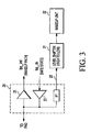
- Fig. 3 is a schematic block diagram of a wake-up architecture in accordance with an embodiment of the present invention.
- Fig. 4 is a schematic block diagram of a wakeup architecture for a multi-package device in accordance with an embodiment of the present invention.
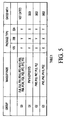
- Fig. 5 is a table showing the decode logic for wakeup gating signals associated with the wakeup architecture of Fig. 4 .
- the present invention provides a semiconductor device having a low power mode and including at least one interface pad, a power management controller (PMC) and a wakeup unit for waking up at least a part of said device from said low power mode, wherein pads are disabled in said low power mode by asserting a power on rest (POR) signal associated with said PMC and wherein a wakeup path is provided to said wakeup unit from an analog power supply associated with said at least one interface pad.
- PMC power management controller
- POR power on rest
- the semiconductor device may comprise a system on a chip (SOC) device.
- the wakeup signal may be applied to the wakeup unit via a high to low level shifter.
- the wakeup signal may be gated via a gating signal indicative of package associated data.
- the gating signal may be obtained from flash memory adapted to store package data associated with the semiconductor device.
- the wakeup signal and the gating signal may be applied to respective inputs of a logical AND gate.
- the gating signal may be applied to the AND gate via a low to high level shifter.
- the output of the AND gate may be applied to the wakeup unit via a high to low level shifter.
- a method of generating a wakeup signal to a wakeup unit associated with a semiconductor device said semiconductor device having a low power mode and including at least one interface pad, a power management controller (PMC) and said wakeup unit.
- the method includes the steps of asserting a power on reset (POR) signal associated with said PMC and generating said wakeup signal from an analog power supply associated with said at least one interface PAD.
- POR power on reset
- a buffer circuit 20 associated with an I/O pad (not shown) in accordance with an embodiment of the invention is shown.
- the buffer circuit 20 includes an input buffer 21 that receives an input signal from the pad and outputs a signal lpp_ind to a wakeup unit (not shown), and an output buffer 22 that receives an internal signal lpp_do and generates an output signal to the pad.
- Power to the buffer circuit 20 may be disabled by asserting the power on reset (POR) signal for the I/O PAD connected to the buffer circuit 20.
- POR power on reset
- a wakeup signal 23 (Pad_res) may be propagated via resistor R1 ( e.g ., 200 ohms).
- the voltage of the wakeup signal 23 (Pad_res) is comparable to the analog supply voltage at the I/O PAD ( e.g ., 3.3 to 5 volts), so preferably the wakeup signal 23 is shifted to core supply level voltage (e.g., 1.2 volts) before being applied to a wakeup unit.
- the POR signal used for the buffer circuit 20 may be the same POR signal that is used for all of the I/O pad buffer circuits, whereas for the conventional buffer circuit 10, a separate POR signal is needed for wakeup buffer circuits.
- FIG. 3 shows a wakeup path for the buffer circuit 20, which includes a level shifter 31 and a wakeup unit 32.
- the wakeup signal 23 from the resistor R1 of the buffer circuit 20 is provided to the level shifter 31, which level shifts the wakeup signal 23.
- the level shifter 31 may be a DC level shifting circuit.
- the level shifting circuit 31 may include an op amp based DC shifting circuit or the like. The output of the level shifting circuit 31 is applied to the wakeup unit 32.
- a single SOC device may be used in multiple packages including packages employing various pin counts. For example, in some packages many of the pads may be unbonded, (i.e., no bond wire connected to the pad) which may cause the corresponding wakeup lines to float. Unbonded pads may also increase functional current in an associated level shifter. To avoid current issues in the level shifter it is desirable to isolate wakeup signals to such unbonded pads.
- Individual pads may be isolated by accessing device options inside a flash memory of an associated microcontroller unit (MCU) to access package associated information or data stored in the flash memory.
- MCU microcontroller unit
- This package data may be used to block certain functionality notwithstanding that such options are generally not accessible to end users.
- the package data is read from the flash memory, decoded, and used to isolate pad wakeup signals that are not being used in a specific package.
- FIG. 4 is a schematic block diagram of a low power architecture for a single die SOC device that may be assembled in multiple package types (e.g. , package types 176, 208, 324 discussed with reference to FIG. 5 below).
- the buffer circuit 20 is connected to an unused or unbonded pad and has the wakeup signal 23 generated from the analog power supply associated with the pad.
- package information is read from the flash memory and provided to decode logic 41 and then is decoded and applied to an input of AND gate 42.
- the output of the AND gate 42 is used to gate the wakeup signal 23 that is provided to the wakeup unit 32.
- the wakeup signal may be level shifted before being provided to the wakeup unit 32 such as with the level shifter 31.
- the decoded package information also may be level shifted (low to high) before being provided to the AND gate 42 with a level shifter 43.
- gating of the wakeup signal (Pad_res) 23 by the AND gate 32 is performed at an analog voltage level (3.3v to 5v) rather than core voltage level (1.2v). Because the voltage obtained from the package decode logic 41 is at the lower core voltage level ( e.g. , 1.2v), the decoded package information signal is shifted to a higher level via the low to high level shifter 43.
- the level shifter 43 may be configured in any suitable manner and by any suitable means.
- the gated wakeup signal at the output of AND gate 42 is at an analog voltage level ( e.g. , 3.3v to 5v)
- the gated wakeup signal needs to be shifted to a lower level (e.g. , 1.2v) via the high to low level shifter 31 before being applied to the wakeup unit 32.
- FIG. 5 is a table including examples of wakeup gating signals Sig1, Sig2, Sig3 associated with package types 176, 208, and 324.
- the table shows that wakeup pads for package type 176 are gated with Sig1.
- Sig1 is logical "1” if the package type is 176 and is logical "0" if the package is not type 176.
- Sig1 is used to gate group "G1" pins ( e.g. , PM10) associated with a package type 176.
- FIG. 5 also shows package types 208 and 324, which are gated with Sig2.
- Sig2 is logical "0” if the package type is 176 and is logical “1” otherwise (not Sig1).
- Sig2 is used to gate group "G2" pins ( e.g. , PM3, PL9, PK7, PL0, PL2) associated with package types 208, 324.
- Table 1 further show that package type 324 is gated with Sig3.
- Sig3 is logical "1” if the package type is 324 and is logical "0” otherwise (not package type 324).
- Sig3 is used to gate group "G3" pins ( e.g. , PN0, PN2, PN10, PO2) associated with a package type 324.
- the proposed wakeup approach eliminates a need to power up wakeup pads in low power mode. Because the approach uses a global POR signal from a PMC to disable I/0 digital devices, a need to safe state I/0 controls in lower power mode may be avoided. This saves gate circuit area and routing overhead.
- the proposed wakeup scheme also works well with a multi-function and multi-purpose design because it does not require special wakeup functionality inside I/O drivers. Also unbonded (e.g., pads not connected to a lead of a lead frame) wakeup I/Os can be marked using package decode bit data to avoid short circuit currents due to floating input signals.
- the present invention provides a low power wakeup architecture for a SoC semiconductor device. While the preferred embodiments of the invention have been illustrated and described, it will be clear that the invention is not limited to these embodiments only. Numerous modifications, changes, variations, substitutions and equivalents will be apparent to those skilled in the art without departing from the spirit and scope of the invention as described in the claims.
Landscapes
- Engineering & Computer Science (AREA)
- Theoretical Computer Science (AREA)
- Physics & Mathematics (AREA)
- General Engineering & Computer Science (AREA)
- General Physics & Mathematics (AREA)
- Power Engineering (AREA)
- Semiconductor Integrated Circuits (AREA)
- Power Sources (AREA)
Abstract
Description
- The present invention relates to semiconductor devices and more particularly, to a low power wake-up architecture for system on a chip (SOC) semiconductor devices including SOC circuitry designed for use with multiple package types and packages employing various pin counts.
- Microcontroller units (MCUs) such as those used in SOCs typically have a low power mode including power gating for a major part of a core of the SOC. To exit from the low power mode, typically an external wakeup source provides a wake-up signal to the SOC through input/output (I/O) pads of the SOC. The I/O pads include I/O buffers for driving loads and/or to provide isolation against external shocks such as electrostatic discharge (ESD).
-
FIG. 1 shows aconventional buffer circuit 10 associated with an I/O pad (not shown) that has aninput buffer 11 that receives an input signal from the I/O pad and generates a wakeup path signal (Ipp_ind). An input signal (Ipp_do) to thebuffer circuit 10 is routed through an output buffer ordriver 12. Thebuffer circuit 10 also receives a power on reset (POR) signal. However, this POR signal is separate from a general POR signal and this separate POR signal is provided to the buffer circuits connected to chip wakeup circuitry. This separate POR signal is inactive in low power mode. - The
output buffer 12 may be disabled in low power mode, butinput buffer 11 remains enabled by keeping the core supply to theinput buffer 11 active to enable the wakeup path, which is shown as "core supply ON" input to thebuffer circuit 10. In order to function, an IO supply to thebuffer circuit 10 also is ON, shown as "IO supply ON". However, keeping theinput buffer 11 active adds significant power overhead that can use an extra 5-10µA of current in a large circuit. - The requirement to provide the core supply to input buffers while in low power mode also presents a physical design overhead since an always ON power supply must be routed to selected pads/buffers. To minimize risk of shorting and avoid current leakage the layout and design of power supplies for pads/buffers should be separated from power supplies that may be OFF in low power mode. However this requirement increases complexity of the pad ring since a separate supply rail is needed to supply these pads/buffers. Customized glue logic may also be required for different pad ring components. Further, such custom logic requirements may not be available for circuits designed using a generic I/O library.
- Therefore, it would be desirable to have a low power architecture for a semiconductor device that does not need to maintain I/O pads in an always ON state. It further would be desirable to be able to remove the requirement of providing a core power supply to the I/O pads.
- The following detailed description of a preferred embodiment will be better understood when read in conjunction with the appended drawings. The present invention is illustrated by way of example and is not limited by the accompanying figures in which like references indicate similar elements. It is to be understood that the drawings are not to scale and have been simplified for ease of understanding the invention.
-
Fig. 1 is a schematic circuit diagram of a conventional I/O pad buffer circuit; -
Fig. 2 is a schematic circuit diagram of an I/O pad buffer circuit with a wakeup path according to one embodiment of the present invention; -
Fig. 3 is a schematic block diagram of a wake-up architecture in accordance with an embodiment of the present invention; and -
Fig. 4 is a schematic block diagram of a wakeup architecture for a multi-package device in accordance with an embodiment of the present invention; and -
Fig. 5 is a table showing the decode logic for wakeup gating signals associated with the wakeup architecture ofFig. 4 . - According to one aspect, the present invention provides a semiconductor device having a low power mode and including at least one interface pad, a power management controller (PMC) and a wakeup unit for waking up at least a part of said device from said low power mode, wherein pads are disabled in said low power mode by asserting a power on rest (POR) signal associated with said PMC and wherein a wakeup path is provided to said wakeup unit from an analog power supply associated with said at least one interface pad. The semiconductor device may comprise a system on a chip (SOC) device.
- The wakeup signal may be applied to the wakeup unit via a high to low level shifter. The wakeup signal may be gated via a gating signal indicative of package associated data. The gating signal may be obtained from flash memory adapted to store package data associated with the semiconductor device.
- The wakeup signal and the gating signal may be applied to respective inputs of a logical AND gate. The gating signal may be applied to the AND gate via a low to high level shifter. The output of the AND gate may be applied to the wakeup unit via a high to low level shifter.
- According to another aspect of the present invention, there is provided a method of generating a wakeup signal to a wakeup unit associated with a semiconductor device, said semiconductor device having a low power mode and including at least one interface pad, a power management controller (PMC) and said wakeup unit. The method includes the steps of asserting a power on reset (POR) signal associated with said PMC and generating said wakeup signal from an analog power supply associated with said at least one interface PAD.
- Referring to
FIG. 2 , abuffer circuit 20 associated with an I/O pad (not shown) in accordance with an embodiment of the invention is shown. Like theconventional buffer circuit 10, thebuffer circuit 20 includes aninput buffer 21 that receives an input signal from the pad and outputs a signal lpp_ind to a wakeup unit (not shown), and anoutput buffer 22 that receives an internal signal lpp_do and generates an output signal to the pad. Power to thebuffer circuit 20 may be disabled by asserting the power on reset (POR) signal for the I/O PAD connected to thebuffer circuit 20. Whenbuffer circuit 20 is in the disabled or low power mode the core supply is OFF or floating. In the disabled or low power mode there is no need to gate control signals associated with the I/O PAD to be at a specific or safe stated level. This may reduce routing complexity of the associated Pad facilitating a reduction of gate count. - Since the core power supply of the
buffer circuit 20 is OFF, an alternative signal is used to wakeup the system. The alternate signal may be obtained via a direct resistive path from the associated pad. In this embodiment of the present invention, a wakeup signal 23 (Pad_res) may be propagated via resistor R1 (e.g., 200 ohms). The voltage of the wakeup signal 23 (Pad_res) is comparable to the analog supply voltage at the I/O PAD (e.g., 3.3 to 5 volts), so preferably thewakeup signal 23 is shifted to core supply level voltage (e.g., 1.2 volts) before being applied to a wakeup unit. Thus, the POR signal used for thebuffer circuit 20 may be the same POR signal that is used for all of the I/O pad buffer circuits, whereas for theconventional buffer circuit 10, a separate POR signal is needed for wakeup buffer circuits. -
FIG. 3 shows a wakeup path for thebuffer circuit 20, which includes alevel shifter 31 and awakeup unit 32. Thewakeup signal 23 from the resistor R1 of thebuffer circuit 20 is provided to thelevel shifter 31, which level shifts thewakeup signal 23. Thelevel shifter 31 may be a DC level shifting circuit. Thelevel shifting circuit 31 may include an op amp based DC shifting circuit or the like. The output of thelevel shifting circuit 31 is applied to thewakeup unit 32. - As discussed above, a single SOC device may be used in multiple packages including packages employing various pin counts. For example, in some packages many of the pads may be unbonded, (i.e., no bond wire connected to the pad) which may cause the corresponding wakeup lines to float. Unbonded pads may also increase functional current in an associated level shifter. To avoid current issues in the level shifter it is desirable to isolate wakeup signals to such unbonded pads.
- Individual pads may be isolated by accessing device options inside a flash memory of an associated microcontroller unit (MCU) to access package associated information or data stored in the flash memory. This package data may be used to block certain functionality notwithstanding that such options are generally not accessible to end users. In one embodiment of the present invention, the package data is read from the flash memory, decoded, and used to isolate pad wakeup signals that are not being used in a specific package.
-
FIG. 4 is a schematic block diagram of a low power architecture for a single die SOC device that may be assembled in multiple package types (e.g.,package types FIG. 5 below). In the embodiment ofFIG. 4 , thebuffer circuit 20 is connected to an unused or unbonded pad and has thewakeup signal 23 generated from the analog power supply associated with the pad. - In order to isolate the wakeup signal since it is associated with an unbonded pad, package information is read from the flash memory and provided to decode
logic 41 and then is decoded and applied to an input of ANDgate 42. The output of the ANDgate 42 is used to gate thewakeup signal 23 that is provided to thewakeup unit 32. As previously discussed, the wakeup signal may be level shifted before being provided to thewakeup unit 32 such as with thelevel shifter 31. The decoded package information also may be level shifted (low to high) before being provided to the ANDgate 42 with alevel shifter 43. - To reduce current leakage, gating of the wakeup signal (Pad_res) 23 by the AND
gate 32 is performed at an analog voltage level (3.3v to 5v) rather than core voltage level (1.2v). Because the voltage obtained from thepackage decode logic 41 is at the lower core voltage level (e.g., 1.2v), the decoded package information signal is shifted to a higher level via the low tohigh level shifter 43. Thelevel shifter 43 may be configured in any suitable manner and by any suitable means. Similarly, because the gated wakeup signal at the output of ANDgate 42 is at an analog voltage level (e.g., 3.3v to 5v), the gated wakeup signal needs to be shifted to a lower level (e.g., 1.2v) via the high tolow level shifter 31 before being applied to thewakeup unit 32. -
FIG. 5 is a table including examples of wakeup gating signals Sig1, Sig2, Sig3 associated withpackage types package type 176 are gated with Sig1. Sig1 is logical "1" if the package type is 176 and is logical "0" if the package is nottype 176. Sig1 is used to gate group "G1" pins (e.g., PM10) associated with apackage type 176. -
FIG. 5 also showspackage types package types - Table 1 further show that
package type 324 is gated with Sig3. Sig3 is logical "1" if the package type is 324 and is logical "0" otherwise (not package type 324). Sig3 is used to gate group "G3" pins (e.g., PN0, PN2, PN10, PO2) associated with apackage type 324. - The proposed wakeup approach eliminates a need to power up wakeup pads in low power mode. Because the approach uses a global POR signal from a PMC to disable I/0 digital devices, a need to safe state I/0 controls in lower power mode may be avoided. This saves gate circuit area and routing overhead.
- The proposed wakeup scheme also works well with a multi-function and multi-purpose design because it does not require special wakeup functionality inside I/O drivers. Also unbonded (e.g., pads not connected to a lead of a lead frame) wakeup I/Os can be marked using package decode bit data to avoid short circuit currents due to floating input signals.
- In a conventional wakeup implementation such features would require customized I/O design or SoC integration as well as software overhead for each package type in order to pull-up unbonded pads.
- As is evident from the foregoing discussion, the present invention provides a low power wakeup architecture for a SoC semiconductor device. While the preferred embodiments of the invention have been illustrated and described, it will be clear that the invention is not limited to these embodiments only. Numerous modifications, changes, variations, substitutions and equivalents will be apparent to those skilled in the art without departing from the spirit and scope of the invention as described in the claims.
Claims (15)
- A semiconductor device having a low power mode, comprising:at least one interface pad;a power management controller (PMC) coupled to said interface pad; anda wakeup unit for waking up at least a part of said semiconductor device from said low power mode, wherein pads are disabled in said low power mode by asserting a power on reset (PoR) signal associated with said PMC and wherein a wakeup signal is generated to said wakeup unit from an analog power supply associated with said at least one interface pad.
- The semiconductor device of claim 1, wherein said semiconductor device includes a system on a chip (SoC) device.
- The semiconductor device of any one of the preceding claims, wherein said wakeup signal is applied to said wakeup unit via a high to low level shifter.
- The semiconductor device of any one of the preceding claims, wherein said wakeup signal is gated via a gating signal indicative of package associated data.
- The semiconductor device of claim 4, wherein said gating signal is obtained from flash memory adapted to store multiple package data associated with said semiconductor device.
- The semiconductor device of claim 4, wherein said wakeup signal and said gating signal are applied to respective inputs of a logical AND gate.
- The semiconductor device of claim 6, wherein said gating signal is applied to said AND gate via a low to high level shifter.
- The semiconductor device of claim 6, wherein the output of said AND gate is applied to said wakeup unit.
- The semiconductor device of claim 8, wherein said output of said AND gate is applied to said wakeup unit via a high to low level shifter.
- A method of generating a wakeup signal to a wakeup unit associated with a semiconductor device, said semiconductor device having a low power mode and including at least one interface pad, a power management controller (PMC) and said wakeup unit, said method including the steps of:asserting a power on reset (POR) signal associated with said PMC; andgenerating said wakeup signal from an analog power supply associated with said at least one interface pad.
- The method of claim 10, wherein said semiconductor device includes a system on a chip (SoC) device.
- The method of claim 10 or 11, including applying said wakeup signal to said wakeup unit via a high to low level shifter.
- The method of claim 10,11 or 12, including gating said wakeup signal via a gating signal indicative of package associated data.
- The method of claim 13, wherein said gating signal is obtained from flash memory adapted to store package data associated with said semiconductor device.
- The method of claim 13 or 14, including applying said wakeup signal and said gating signal to respective inputs of a logical AND gate.
Applications Claiming Priority (1)
| Application Number | Priority Date | Filing Date | Title |
|---|---|---|---|
| US13/214,164 US8543856B2 (en) | 2011-08-20 | 2011-08-20 | Semiconductor device with wake-up unit |
Related Parent Applications (2)
| Application Number | Title | Priority Date | Filing Date |
|---|---|---|---|
| US201113214164 Previously-Filed-Application | 2011-08-20 | ||
| US13/214,164 Previously-Filed-Application US8543856B2 (en) | 2011-08-20 | 2011-08-20 | Semiconductor device with wake-up unit |
Publications (2)
| Publication Number | Publication Date |
|---|---|
| EP2562619A1 true EP2562619A1 (en) | 2013-02-27 |
| EP2562619B1 EP2562619B1 (en) | 2014-06-04 |
Family
ID=47076061
Family Applications (1)
| Application Number | Title | Priority Date | Filing Date |
|---|---|---|---|
| EP12179294.9A Active EP2562619B1 (en) | 2011-08-20 | 2012-08-03 | Semiconductor device with wake-up unit |
Country Status (5)
| Country | Link |
|---|---|
| US (1) | US8543856B2 (en) |
| EP (1) | EP2562619B1 (en) |
| JP (1) | JP6172835B2 (en) |
| KR (1) | KR20130020759A (en) |
| CN (1) | CN102955441B (en) |
Families Citing this family (8)
| Publication number | Priority date | Publication date | Assignee | Title |
|---|---|---|---|---|
| KR102088865B1 (en) * | 2012-09-03 | 2020-03-13 | 가부시키가이샤 한도오따이 에네루기 켄큐쇼 | Microcontroller |
| KR102168987B1 (en) | 2012-10-17 | 2020-10-22 | 가부시키가이샤 한도오따이 에네루기 켄큐쇼 | Microcontroller and method for manufacturing the same |
| KR20140122567A (en) * | 2013-04-10 | 2014-10-20 | 에스케이하이닉스 주식회사 | Semiconductor memory device including power on reset circuit |
| US9494987B2 (en) | 2013-11-30 | 2016-11-15 | Freescale Semiconductor, Inc. | Processing system with low power wake-up pad |
| CN106033960B (en) * | 2015-03-16 | 2019-04-26 | 上海贝岭股份有限公司 | A kind of power-on-reset circuit with low power consumption |
| KR20200033690A (en) * | 2018-09-20 | 2020-03-30 | 에스케이하이닉스 주식회사 | Semiconductor device executing a method for controlling a power down mode |
| US11047904B2 (en) * | 2019-03-05 | 2021-06-29 | Nxp Usa, Inc. | Low power mode testing in an integrated circuit |
| US11994888B2 (en) | 2022-07-18 | 2024-05-28 | Nxp Usa, Inc. | Power supply handling for multiple package configurations |
Citations (3)
| Publication number | Priority date | Publication date | Assignee | Title |
|---|---|---|---|---|
| US20080162969A1 (en) * | 2006-12-28 | 2008-07-03 | Texas Instruments Incorporated | Detecting wake-up events for a chip based on an i/o power supply |
| US20100205467A1 (en) * | 2009-02-06 | 2010-08-12 | Samsung Electronics Co., Ltd. | Low-power system-on-chip |
| US20110185199A1 (en) * | 2010-01-28 | 2011-07-28 | Hon Hai Precision Industry Co., Ltd. | Embedded system and power saving method thereof |
Family Cites Families (20)
| Publication number | Priority date | Publication date | Assignee | Title |
|---|---|---|---|---|
| JPH0283678A (en) * | 1988-09-20 | 1990-03-23 | Hitachi Ltd | How to develop a data processing system |
| US5400237A (en) * | 1992-05-11 | 1995-03-21 | Simmonds Precision Products, Inc. | PWM inverter controller with waveform memory |
| JP2570955B2 (en) * | 1993-03-12 | 1997-01-16 | ヤマハ株式会社 | Display lifting device |
| JP2001100869A (en) * | 1999-09-27 | 2001-04-13 | Toshiba Lsi System Support Kk | Circuit for reducing current consumption in standby state in microcomputer-mounted devices |
| US6886105B2 (en) | 2000-02-14 | 2005-04-26 | Intel Corporation | Method and apparatus for resuming memory operations from a low latency wake-up low power state |
| US6760850B1 (en) * | 2000-07-31 | 2004-07-06 | Hewlett-Packard Development Company, L.P. | Method and apparatus executing power on self test code to enable a wakeup device for a computer system responsive to detecting an AC power source |
| US7109865B2 (en) | 2002-09-26 | 2006-09-19 | Massachusetts Institute Of Technology | Tag interrogation with observable response signal |
| JP3810361B2 (en) * | 2002-11-01 | 2006-08-16 | 松下電器産業株式会社 | Semiconductor integrated circuit and interrupt request output method for semiconductor integrated circuit |
| JP3807407B2 (en) * | 2003-09-05 | 2006-08-09 | セイコーエプソン株式会社 | Transmitter circuit, receiver circuit, interface circuit, and electronic device |
| JP4832721B2 (en) * | 2004-02-25 | 2011-12-07 | 富士通セミコンダクター株式会社 | Semiconductor device and microcontroller |
| KR100727926B1 (en) | 2004-10-23 | 2007-06-14 | 삼성전자주식회사 | Power management method and apparatus of portable information terminal device |
| KR20060041451A (en) | 2004-11-09 | 2006-05-12 | 삼성전기주식회사 | Wake-Up System Using Oscillation |
| KR100692991B1 (en) | 2005-02-04 | 2007-03-12 | 삼성전자주식회사 | Wake-up terminal using extremely low power and its wake-up method |
| JP4713901B2 (en) * | 2005-02-24 | 2011-06-29 | ルネサスエレクトロニクス株式会社 | Semiconductor integrated circuit device |
| KR100790711B1 (en) | 2006-11-03 | 2008-01-02 | 삼성전기주식회사 | Ultra Low Power Wake-Up Receiver |
| US7583104B2 (en) | 2006-12-12 | 2009-09-01 | Microchip Technology Incorporated | Maintaining input and/or output configuration and data state during and when coming out of a low power mode |
| KR100909067B1 (en) | 2007-12-18 | 2009-07-23 | 한국전자통신연구원 | Wake-up Receiver and Wake-up Method Using Constant Cyclic Power Shutdown |
| US9189048B2 (en) | 2008-09-10 | 2015-11-17 | Apple Inc. | Circuit having a low power mode |
| WO2010032091A1 (en) | 2008-09-19 | 2010-03-25 | Freescale Semiconductor, Inc. | Wake-up control system and method for controlling receiver wake-up |
| JP5954191B2 (en) * | 2013-01-17 | 2016-07-20 | 株式会社デンソー | Power circuit |
-
2011
- 2011-08-20 US US13/214,164 patent/US8543856B2/en active Active
-
2012
- 2012-07-31 JP JP2012169983A patent/JP6172835B2/en active Active
- 2012-08-03 EP EP12179294.9A patent/EP2562619B1/en active Active
- 2012-08-17 KR KR1020120090177A patent/KR20130020759A/en not_active Withdrawn
- 2012-08-20 CN CN201210296941.5A patent/CN102955441B/en active Active
Patent Citations (3)
| Publication number | Priority date | Publication date | Assignee | Title |
|---|---|---|---|---|
| US20080162969A1 (en) * | 2006-12-28 | 2008-07-03 | Texas Instruments Incorporated | Detecting wake-up events for a chip based on an i/o power supply |
| US20100205467A1 (en) * | 2009-02-06 | 2010-08-12 | Samsung Electronics Co., Ltd. | Low-power system-on-chip |
| US20110185199A1 (en) * | 2010-01-28 | 2011-07-28 | Hon Hai Precision Industry Co., Ltd. | Embedded system and power saving method thereof |
Also Published As
| Publication number | Publication date |
|---|---|
| US20130047016A1 (en) | 2013-02-21 |
| US8543856B2 (en) | 2013-09-24 |
| JP6172835B2 (en) | 2017-08-02 |
| KR20130020759A (en) | 2013-02-28 |
| CN102955441A (en) | 2013-03-06 |
| JP2013045453A (en) | 2013-03-04 |
| CN102955441B (en) | 2017-04-12 |
| EP2562619B1 (en) | 2014-06-04 |
Similar Documents
| Publication | Publication Date | Title |
|---|---|---|
| EP2562619B1 (en) | Semiconductor device with wake-up unit | |
| US9362909B2 (en) | System and method for reducing reconfiguration power usage | |
| KR101420559B1 (en) | Distributed power delivery scheme for on-die voltage scaling | |
| US20090057417A1 (en) | Ic card | |
| US20080082842A1 (en) | Power supply control circuit of subsystem and subsystem | |
| JP2010515277A (en) | System, method, and integrated circuit having an inrush limiting power island | |
| CN114900020A (en) | Multi-input single-output power supply system and working method thereof | |
| EP1649493A2 (en) | Nested voltage island architecture | |
| US9503288B2 (en) | Display driver capable of driving multiple display interfaces | |
| US9042172B2 (en) | Flash memory having dual supply operation | |
| US8762753B2 (en) | Power management circuit using two configuration signals to control the power modes of two circuit modules using two crosslinked multiplexers and a level shifter | |
| US20140351608A1 (en) | Power management in a discrete memory portion | |
| CN115769173A (en) | Systems and methods for adaptive power multiplexing | |
| JP2005175489A (en) | Low power semiconductor chip with isolated power ring and method for manufacturing and controlling the same | |
| US9331673B2 (en) | Integrated circuit operating active circuitry and chip pads in different operating modes and at different voltage levels | |
| US9391618B2 (en) | High voltage fail-safe IO design using thin oxide devices | |
| US6930514B2 (en) | Method and apparatus for transferring data between data buses | |
| US10164432B2 (en) | Systems, methods, and apparatus for powering devices using energy from a communication bus | |
| US9385690B1 (en) | Integrated circuit with multiplexed I/O pads | |
| JP7801017B2 (en) | Low-overhead, high-bandwidth reconfigurable interconnect apparatus and method | |
| JP2007027401A (en) | Semiconductor device | |
| JP2001147746A (en) | Power supply circuit of microcomputer | |
| JP2008112788A (en) | Semiconductor device |
Legal Events
| Date | Code | Title | Description |
|---|---|---|---|
| PUAI | Public reference made under article 153(3) epc to a published international application that has entered the european phase |
Free format text: ORIGINAL CODE: 0009012 |
|
| AK | Designated contracting states |
Kind code of ref document: A1 Designated state(s): AL AT BE BG CH CY CZ DE DK EE ES FI FR GB GR HR HU IE IS IT LI LT LU LV MC MK MT NL NO PL PT RO RS SE SI SK SM TR |
|
| AX | Request for extension of the european patent |
Extension state: BA ME |
|
| 17P | Request for examination filed |
Effective date: 20130827 |
|
| RBV | Designated contracting states (corrected) |
Designated state(s): AL AT BE BG CH CY CZ DE DK EE ES FI FR GB GR HR HU IE IS IT LI LT LU LV MC MK MT NL NO PL PT RO RS SE SI SK SM TR |
|
| GRAP | Despatch of communication of intention to grant a patent |
Free format text: ORIGINAL CODE: EPIDOSNIGR1 |
|
| INTG | Intention to grant announced |
Effective date: 20140102 |
|
| GRAS | Grant fee paid |
Free format text: ORIGINAL CODE: EPIDOSNIGR3 |
|
| GRAA | (expected) grant |
Free format text: ORIGINAL CODE: 0009210 |
|
| AK | Designated contracting states |
Kind code of ref document: B1 Designated state(s): AL AT BE BG CH CY CZ DE DK EE ES FI FR GB GR HR HU IE IS IT LI LT LU LV MC MK MT NL NO PL PT RO RS SE SI SK SM TR |
|
| REG | Reference to a national code |
Ref country code: GB Ref legal event code: FG4D |
|
| REG | Reference to a national code |
Ref country code: CH Ref legal event code: EP |
|
| REG | Reference to a national code |
Ref country code: AT Ref legal event code: REF Ref document number: 671412 Country of ref document: AT Kind code of ref document: T Effective date: 20140615 |
|
| REG | Reference to a national code |
Ref country code: IE Ref legal event code: FG4D |
|
| REG | Reference to a national code |
Ref country code: DE Ref legal event code: R096 Ref document number: 602012001968 Country of ref document: DE Effective date: 20140717 |
|
| REG | Reference to a national code |
Ref country code: AT Ref legal event code: MK05 Ref document number: 671412 Country of ref document: AT Kind code of ref document: T Effective date: 20140604 |
|
| REG | Reference to a national code |
Ref country code: NL Ref legal event code: VDEP Effective date: 20140604 |
|
| PG25 | Lapsed in a contracting state [announced via postgrant information from national office to epo] |
Ref country code: LT Free format text: LAPSE BECAUSE OF FAILURE TO SUBMIT A TRANSLATION OF THE DESCRIPTION OR TO PAY THE FEE WITHIN THE PRESCRIBED TIME-LIMIT Effective date: 20140604 Ref country code: NO Free format text: LAPSE BECAUSE OF FAILURE TO SUBMIT A TRANSLATION OF THE DESCRIPTION OR TO PAY THE FEE WITHIN THE PRESCRIBED TIME-LIMIT Effective date: 20140904 Ref country code: GR Free format text: LAPSE BECAUSE OF FAILURE TO SUBMIT A TRANSLATION OF THE DESCRIPTION OR TO PAY THE FEE WITHIN THE PRESCRIBED TIME-LIMIT Effective date: 20140905 Ref country code: FI Free format text: LAPSE BECAUSE OF FAILURE TO SUBMIT A TRANSLATION OF THE DESCRIPTION OR TO PAY THE FEE WITHIN THE PRESCRIBED TIME-LIMIT Effective date: 20140604 Ref country code: CY Free format text: LAPSE BECAUSE OF FAILURE TO SUBMIT A TRANSLATION OF THE DESCRIPTION OR TO PAY THE FEE WITHIN THE PRESCRIBED TIME-LIMIT Effective date: 20140604 |
|
| REG | Reference to a national code |
Ref country code: LT Ref legal event code: MG4D |
|
| PG25 | Lapsed in a contracting state [announced via postgrant information from national office to epo] |
Ref country code: SE Free format text: LAPSE BECAUSE OF FAILURE TO SUBMIT A TRANSLATION OF THE DESCRIPTION OR TO PAY THE FEE WITHIN THE PRESCRIBED TIME-LIMIT Effective date: 20140604 Ref country code: AT Free format text: LAPSE BECAUSE OF FAILURE TO SUBMIT A TRANSLATION OF THE DESCRIPTION OR TO PAY THE FEE WITHIN THE PRESCRIBED TIME-LIMIT Effective date: 20140604 Ref country code: HR Free format text: LAPSE BECAUSE OF FAILURE TO SUBMIT A TRANSLATION OF THE DESCRIPTION OR TO PAY THE FEE WITHIN THE PRESCRIBED TIME-LIMIT Effective date: 20140604 Ref country code: LV Free format text: LAPSE BECAUSE OF FAILURE TO SUBMIT A TRANSLATION OF THE DESCRIPTION OR TO PAY THE FEE WITHIN THE PRESCRIBED TIME-LIMIT Effective date: 20140604 Ref country code: RS Free format text: LAPSE BECAUSE OF FAILURE TO SUBMIT A TRANSLATION OF THE DESCRIPTION OR TO PAY THE FEE WITHIN THE PRESCRIBED TIME-LIMIT Effective date: 20140604 |
|
| PGFP | Annual fee paid to national office [announced via postgrant information from national office to epo] |
Ref country code: FR Payment date: 20140818 Year of fee payment: 3 |
|
| PG25 | Lapsed in a contracting state [announced via postgrant information from national office to epo] |
Ref country code: CZ Free format text: LAPSE BECAUSE OF FAILURE TO SUBMIT A TRANSLATION OF THE DESCRIPTION OR TO PAY THE FEE WITHIN THE PRESCRIBED TIME-LIMIT Effective date: 20140604 Ref country code: SK Free format text: LAPSE BECAUSE OF FAILURE TO SUBMIT A TRANSLATION OF THE DESCRIPTION OR TO PAY THE FEE WITHIN THE PRESCRIBED TIME-LIMIT Effective date: 20140604 Ref country code: ES Free format text: LAPSE BECAUSE OF FAILURE TO SUBMIT A TRANSLATION OF THE DESCRIPTION OR TO PAY THE FEE WITHIN THE PRESCRIBED TIME-LIMIT Effective date: 20140604 Ref country code: RO Free format text: LAPSE BECAUSE OF FAILURE TO SUBMIT A TRANSLATION OF THE DESCRIPTION OR TO PAY THE FEE WITHIN THE PRESCRIBED TIME-LIMIT Effective date: 20140604 Ref country code: EE Free format text: LAPSE BECAUSE OF FAILURE TO SUBMIT A TRANSLATION OF THE DESCRIPTION OR TO PAY THE FEE WITHIN THE PRESCRIBED TIME-LIMIT Effective date: 20140604 Ref country code: PT Free format text: LAPSE BECAUSE OF FAILURE TO SUBMIT A TRANSLATION OF THE DESCRIPTION OR TO PAY THE FEE WITHIN THE PRESCRIBED TIME-LIMIT Effective date: 20141006 |
|
| PG25 | Lapsed in a contracting state [announced via postgrant information from national office to epo] |
Ref country code: PL Free format text: LAPSE BECAUSE OF FAILURE TO SUBMIT A TRANSLATION OF THE DESCRIPTION OR TO PAY THE FEE WITHIN THE PRESCRIBED TIME-LIMIT Effective date: 20140604 Ref country code: IS Free format text: LAPSE BECAUSE OF FAILURE TO SUBMIT A TRANSLATION OF THE DESCRIPTION OR TO PAY THE FEE WITHIN THE PRESCRIBED TIME-LIMIT Effective date: 20141004 Ref country code: NL Free format text: LAPSE BECAUSE OF FAILURE TO SUBMIT A TRANSLATION OF THE DESCRIPTION OR TO PAY THE FEE WITHIN THE PRESCRIBED TIME-LIMIT Effective date: 20140604 |
|
| REG | Reference to a national code |
Ref country code: DE Ref legal event code: R097 Ref document number: 602012001968 Country of ref document: DE |
|
| PG25 | Lapsed in a contracting state [announced via postgrant information from national office to epo] |
Ref country code: LU Free format text: LAPSE BECAUSE OF FAILURE TO SUBMIT A TRANSLATION OF THE DESCRIPTION OR TO PAY THE FEE WITHIN THE PRESCRIBED TIME-LIMIT Effective date: 20140803 Ref country code: MC Free format text: LAPSE BECAUSE OF FAILURE TO SUBMIT A TRANSLATION OF THE DESCRIPTION OR TO PAY THE FEE WITHIN THE PRESCRIBED TIME-LIMIT Effective date: 20140604 |
|
| PLBE | No opposition filed within time limit |
Free format text: ORIGINAL CODE: 0009261 |
|
| STAA | Information on the status of an ep patent application or granted ep patent |
Free format text: STATUS: NO OPPOSITION FILED WITHIN TIME LIMIT |
|
| PG25 | Lapsed in a contracting state [announced via postgrant information from national office to epo] |
Ref country code: BE Free format text: LAPSE BECAUSE OF NON-PAYMENT OF DUE FEES Effective date: 20140831 Ref country code: IT Free format text: LAPSE BECAUSE OF FAILURE TO SUBMIT A TRANSLATION OF THE DESCRIPTION OR TO PAY THE FEE WITHIN THE PRESCRIBED TIME-LIMIT Effective date: 20140604 Ref country code: DK Free format text: LAPSE BECAUSE OF FAILURE TO SUBMIT A TRANSLATION OF THE DESCRIPTION OR TO PAY THE FEE WITHIN THE PRESCRIBED TIME-LIMIT Effective date: 20140604 |
|
| 26N | No opposition filed |
Effective date: 20150305 |
|
| REG | Reference to a national code |
Ref country code: IE Ref legal event code: MM4A |
|
| REG | Reference to a national code |
Ref country code: DE Ref legal event code: R097 Ref document number: 602012001968 Country of ref document: DE Effective date: 20150305 |
|
| PG25 | Lapsed in a contracting state [announced via postgrant information from national office to epo] |
Ref country code: BE Free format text: LAPSE BECAUSE OF FAILURE TO SUBMIT A TRANSLATION OF THE DESCRIPTION OR TO PAY THE FEE WITHIN THE PRESCRIBED TIME-LIMIT Effective date: 20140604 |
|
| PG25 | Lapsed in a contracting state [announced via postgrant information from national office to epo] |
Ref country code: SI Free format text: LAPSE BECAUSE OF FAILURE TO SUBMIT A TRANSLATION OF THE DESCRIPTION OR TO PAY THE FEE WITHIN THE PRESCRIBED TIME-LIMIT Effective date: 20140604 |
|
| PG25 | Lapsed in a contracting state [announced via postgrant information from national office to epo] |
Ref country code: IE Free format text: LAPSE BECAUSE OF NON-PAYMENT OF DUE FEES Effective date: 20140803 |
|
| REG | Reference to a national code |
Ref country code: CH Ref legal event code: PL |
|
| PG25 | Lapsed in a contracting state [announced via postgrant information from national office to epo] |
Ref country code: LI Free format text: LAPSE BECAUSE OF NON-PAYMENT OF DUE FEES Effective date: 20150831 Ref country code: CH Free format text: LAPSE BECAUSE OF NON-PAYMENT OF DUE FEES Effective date: 20150831 |
|
| PG25 | Lapsed in a contracting state [announced via postgrant information from national office to epo] |
Ref country code: SM Free format text: LAPSE BECAUSE OF FAILURE TO SUBMIT A TRANSLATION OF THE DESCRIPTION OR TO PAY THE FEE WITHIN THE PRESCRIBED TIME-LIMIT Effective date: 20140604 |
|
| REG | Reference to a national code |
Ref country code: FR Ref legal event code: ST Effective date: 20160429 |
|
| PG25 | Lapsed in a contracting state [announced via postgrant information from national office to epo] |
Ref country code: BG Free format text: LAPSE BECAUSE OF FAILURE TO SUBMIT A TRANSLATION OF THE DESCRIPTION OR TO PAY THE FEE WITHIN THE PRESCRIBED TIME-LIMIT Effective date: 20140604 Ref country code: MT Free format text: LAPSE BECAUSE OF FAILURE TO SUBMIT A TRANSLATION OF THE DESCRIPTION OR TO PAY THE FEE WITHIN THE PRESCRIBED TIME-LIMIT Effective date: 20140604 |
|
| PG25 | Lapsed in a contracting state [announced via postgrant information from national office to epo] |
Ref country code: TR Free format text: LAPSE BECAUSE OF FAILURE TO SUBMIT A TRANSLATION OF THE DESCRIPTION OR TO PAY THE FEE WITHIN THE PRESCRIBED TIME-LIMIT Effective date: 20140604 Ref country code: HU Free format text: LAPSE BECAUSE OF FAILURE TO SUBMIT A TRANSLATION OF THE DESCRIPTION OR TO PAY THE FEE WITHIN THE PRESCRIBED TIME-LIMIT; INVALID AB INITIO Effective date: 20120803 |
|
| PG25 | Lapsed in a contracting state [announced via postgrant information from national office to epo] |
Ref country code: FR Free format text: LAPSE BECAUSE OF NON-PAYMENT OF DUE FEES Effective date: 20150831 |
|
| REG | Reference to a national code |
Ref country code: GB Ref legal event code: 732E Free format text: REGISTERED BETWEEN 20171109 AND 20171115 |
|
| REG | Reference to a national code |
Ref country code: DE Ref legal event code: R081 Ref document number: 602012001968 Country of ref document: DE Owner name: NXP USA, INC. (N.D.GES.D.STAATES DELAWARE), AU, US Free format text: FORMER OWNER: FREESCALE SEMICONDUCTOR, INC., AUSTIN, TEX., US |
|
| PG25 | Lapsed in a contracting state [announced via postgrant information from national office to epo] |
Ref country code: MK Free format text: LAPSE BECAUSE OF FAILURE TO SUBMIT A TRANSLATION OF THE DESCRIPTION OR TO PAY THE FEE WITHIN THE PRESCRIBED TIME-LIMIT Effective date: 20140604 |
|
| PG25 | Lapsed in a contracting state [announced via postgrant information from national office to epo] |
Ref country code: AL Free format text: LAPSE BECAUSE OF FAILURE TO SUBMIT A TRANSLATION OF THE DESCRIPTION OR TO PAY THE FEE WITHIN THE PRESCRIBED TIME-LIMIT Effective date: 20140604 |
|
| P01 | Opt-out of the competence of the unified patent court (upc) registered |
Effective date: 20230725 |
|
| PGFP | Annual fee paid to national office [announced via postgrant information from national office to epo] |
Ref country code: DE Payment date: 20250724 Year of fee payment: 14 |
|
| PGFP | Annual fee paid to national office [announced via postgrant information from national office to epo] |
Ref country code: GB Payment date: 20250724 Year of fee payment: 14 |