EP2562534A2 - Method for analyzing rubber compound with filler particles - Google Patents
Method for analyzing rubber compound with filler particles Download PDFInfo
- Publication number
- EP2562534A2 EP2562534A2 EP12175905A EP12175905A EP2562534A2 EP 2562534 A2 EP2562534 A2 EP 2562534A2 EP 12175905 A EP12175905 A EP 12175905A EP 12175905 A EP12175905 A EP 12175905A EP 2562534 A2 EP2562534 A2 EP 2562534A2
- Authority
- EP
- European Patent Office
- Prior art keywords
- rubber compound
- specimen
- stem
- finite element
- rubber
- Prior art date
- Legal status (The legal status is an assumption and is not a legal conclusion. Google has not performed a legal analysis and makes no representation as to the accuracy of the status listed.)
- Withdrawn
Links
Images








Classifications
-
- G—PHYSICS
- G01—MEASURING; TESTING
- G01N—INVESTIGATING OR ANALYSING MATERIALS BY DETERMINING THEIR CHEMICAL OR PHYSICAL PROPERTIES
- G01N23/00—Investigating or analysing materials by the use of wave or particle radiation, e.g. X-rays or neutrons, not covered by groups G01N3/00 – G01N17/00, G01N21/00 or G01N22/00
- G01N23/02—Investigating or analysing materials by the use of wave or particle radiation, e.g. X-rays or neutrons, not covered by groups G01N3/00 – G01N17/00, G01N21/00 or G01N22/00 by transmitting the radiation through the material
- G01N23/06—Investigating or analysing materials by the use of wave or particle radiation, e.g. X-rays or neutrons, not covered by groups G01N3/00 – G01N17/00, G01N21/00 or G01N22/00 by transmitting the radiation through the material and measuring the absorption
- G01N23/18—Investigating the presence of flaws defects or foreign matter
-
- G—PHYSICS
- G01—MEASURING; TESTING
- G01N—INVESTIGATING OR ANALYSING MATERIALS BY DETERMINING THEIR CHEMICAL OR PHYSICAL PROPERTIES
- G01N2223/00—Investigating materials by wave or particle radiation
- G01N2223/60—Specific applications or type of materials
- G01N2223/607—Specific applications or type of materials strain
Definitions
- the present invention relates to a method for analyzing rubber compound with filler particles, more particularly to a method in which the dispersion of filler particles can be clearly analyzed.
- rubber compounds used in rubber products e.g. tires and the like contain fillers, e.g. carbon black, silica and the like as reinforcing agents. It is generally known in the art that a dispersion of such filler particles in a rubber compound affects characteristics such as strength of the rubber compound. Therefore, it has been desired that the dispersion of filler particles in the rubber compound can be clearly analyzed.
- a method for analyzing rubber compound including a rubber component and filler particles comprises:
- the rubber component (a) can be, for example, natural rubber (NR), isoprene rubber (IR), butyl rubber (IIR), butadiene rubber (BR), styrene butadiene rubber (SBR), styrene isoprene butadiene rubber (SIBR), ethylene-propylene-diene rubber (EPDM), chloroprene rubber (CR), acrylonitrile butadiene rubber (NBR) and the like.
- NR natural rubber
- IR isoprene rubber
- IIR butyl rubber
- BR butadiene rubber
- SBR styrene butadiene rubber
- SIBR styrene isoprene butadiene rubber
- EPDM ethylene-propylene-diene rubber
- CR chloroprene rubber
- NBR acrylonitrile butadiene rubber
- the filler (b) can be carbon black, silica, clay, talc, magnesium carbonate, magnesium hydroxide and the like of course the rubber component (a) and filler (b) are not limited to these examples. Further, various additives, e.g. sulfur, vulcanization accelerator and the like may be added in the rubber compound (c). In this embodiment, a slice of the rubber compound with a constant thickness (t) is used as a specimen 5 (shown in Fig. 3 ).
- FIG. 2 A flow chart implementing the analyzing method as an embodiment of the present invention is shown in Fig. 2 . This method comprises the following steps S1-S5.
- the scanning transmission electron microscope (STEM) 100 comprises: an electron gun 1 directed perpendicularly to a horizontal plane and capable of emitting electrons downward; a focusing lens 3 for focusing the electrons as an electron beam 2 on the specimen 5 of the rubber compound (c); scanning coils 4 including an X-direction scanning coil 4X and a Y-direction scanning coil 4Y for deflecting the electron beam 2 in the X-direction and Y-direction to scan the specimen 5; a specimen holder 6 for holding the specimen 5; and a specimen stage 9 on which the specimen holder 6 is detachably fixed.
- STEM scanning transmission electron microscope
- an electron beam pass-through hole 8 is formed along the central axis (o) of the scanning transmission electron microscope 100 so that transmission electrons 7 which penetrate through the specimen 5 can pass through the hole 8.
- an electron beam pass-through hole 10 is formed along the central axis (o) and continuously from the electron beam pass-through hole 8 so that the transmission electrons 7 can pass through the hole 10.
- the detector 20 for the transmission electrons 15 passing through the aperture 11.
- the detector 20 comprises a scintillator 13 and a photoelectron multiplier tube 14.
- the scintillator 13 reemits the energy of the incident electrons 12 passing though the aperture 11, in the form of light.
- the microscope 100 is used to acquire STEM images of the rubber compound (c) as follows. First, the specimen holder 6 with the specimen 5 is attached to the specimen stage 9 by an operating personnel.
- the outgoing electrons 7 travel through the holes 8 and 10 to the scattering angle limiting aperture 11 which allows the electrons having particular scattering angles to pass through it.
- the electrons 12 passing through the scattering angle limiting aperture 11 go into the scintillator 13, and thereby the energy of the incident electrons 12 is reemitted in the form of light. Then by the accompanying photoelectron multiplier tube 14, the light is converted to an electronic signal. The electrical signal is amplified and converted to digital data by an amplifier and A/D converter (not shown). The digital data are transmitted to a display (not shown) in which, according to the transmitted signal, brightness modulation is made, and an electron beam transmission image reflecting the internal structure of the specimen 5 is displayed as a STEM image, and at the same time, the digital data are stored in a memory of the computer. Thus, a plurality of STEM images corresponding to the scan positions are acquired as the STEM images' dataset.
- the intensity and scattering angle of the outgoing electrons 7 are varied depending on the internal state, thickness and/or atomic species of the specimen 5.
- the scattering angle is also varied by the accelerating voltage. For example, if the accelerating voltage is decreased, the electrons are scattered more in the specimen 5, and the scattering angle or outgoing angle from the lower surface of the specimen 5 with respect to the central axis (o) is increased.
- the camera length L1 namely the distance between the specimen 5 and the scintillator 13 is preferably set in a range of from 8 to 150 cm.
- the accelerating voltage for the electron beam may be set in a range of 100 to 3000 kv depending on the specimen 5.
- the STEM image acquiring step S1 in this embodiment a plurality of images of the rubber compound (c) are took from different angles with respect to the central axis (o) of the scanning transmission electron microscope 100.
- the microscope 100 is provided with a specimen tilting device (not shown) to tilt the specimen 5 with respect to the central axis (o) with this, as shown in Fig. 5 , the specimen 5 can be held at different tilt angles ⁇ with respect to a horizontal plane H.
- the computer outputs a control signal to the specimen tilting device and according thereto the device tilts the specimen 5 at a specific angle ⁇ .
- variable range of the tilt angle ⁇ of the specimen 5 is -90 to +90 degrees, preferably -70 to +70 degrees. However, if the specimen is a round bar of the rubber compound, the variable range of the angle ⁇ may be -180 to +180 degrees.
- the specimen 5 is tilted at a measuring start angle ⁇ and in this tilted state, the STEM images or the dataset thereof are acquired as explained above. Then, until a measuring stop angle ⁇ , the process of changing the tilt angle of the specimen 5 and acquiring the dataset of the STEM images of the specimen 5 at that tilt angle are repeated at a step in a range of from 0.5 to 4 degrees, preferably 1 to 2 degrees in order to obtain the after-mentioned slice images clearly and efficiently.
- the measuring start angle ⁇ and measuring stop angle ⁇ can be arbitrarily set on the microscope by using a controller.
- the measuring start angle ⁇ is +70 degrees
- the measuring stop angle ⁇ is -70 degrees.
- the focal point F of the electron beam (e) is set in a thickness center region C of the specimen 5 as shown in Fig. 6(a) .
- the focal point F of the electron beam (e) when the focal point F of the electron beam (e) is set in the thickness center region C of the specimen 5 as shown in Fig. 6(a) , the range on the specimen 5 in which a clear image can be obtained becomes increased. It is desirable that the depth (f) of field can completely overlaps or encompass the thickness (t) of the specimen 5.
- the upper surface 5a and the lower surface 5b of the specimen 5 are perpendicular to the electron beam axis (namely, the incidence angle is equal to 90 deg.).
- the upper surface 5a and the lower surface 5b of the specimen 5 are inclined with respect to the electron beam axis (namely, the incidence angle is not equal to 90 deg.). Under such inclined state, the thickness of the specimen 5 measured along the electron beam axis is referred to as apparent thickness (t') in contrast to the real thickness (t) measured perpendicularly to the upper surface 5a.
- ⁇ is the tilt angle of the specimen 5 with respect to the horizontal plane, as shown in Fig. 6(b) .
- the central region C within which the focal point F is set ranges 30 %, preferably 20 %, more preferably 10 % of the real/apparent thickness.
- the central region C may be off-centered, but preferably it is centered on the center of the real/apparent thickness.
- the real thickness (t) may be less than 200 nm as usual, but it is preferably set in a range of from 200 to 1500 nm, more preferably 500 to 1000 nm.
- the focal point F is adjusted by the focusing lens 3 and/or specimen stage 9 by the use of a focal point adjuster of the microscope system 100.
- a three-dimensional structure of the rubber compound is reconstructed as numerical data (hereinafter the "3D dataset") by executing a tomographic method with the computer, and the 3D dataset is stored in a memory of the computer.
- those acquired by changing the tilt angle of the specimen 5 as explained above can be preferably used. But, it is also possible to use those acquired by not changing the tilt angle, namely acquired at a single tilt angle of the specimen 5 preferably zero degree with respect to the horizontal plane.
- Fig. 8 shows such created image which is a perspective view of the filler particles dispersed in the rubber compound.
- slice images of the rubber compound (c) taken along predetermined sections of the rubber compound (c) are reconstructed by the computer as numerical data (herein after the "slice image dataset"), and the slice image dataset is stored in a memory of the computer.
- the above-mentioned predetermined sections of the rubber compound can be arbitrarily determined according to the coordinate system (Cartesian or polar or cylindrical) employed in the subsequent step S4.
- Step S4 a finite element model of the rubber compound (c) is generated based on the slice image of the rubber compound (c).
- Step S4 further comprises a first step S41, a second step S42 and a third step S43.
- a first finite element model 5a of the rubber compound is set using only regular elements each with the same shape, as shown in Fig. 9(a) .
- the slice image is subjected to an image processing to divide the entire region of the slice image into a domain of the rubber component (a), a domain of the filler particle (b) and/or a domain of other component if any.
- the image processing method a known method can be used in which, based on threshold levels of gray level, micro regions of the slice image are each identified whether it is a rubber domain or a filler domain (or other domain if any).
- At least one slice image including at least two domains of the rubber component (a) and filler particles (b) is divided by using only regular elements eb each with the same shape, to generate a first finite element model of the rubber compound (c).
- Fig. 9(a) shows a small part of the first finite element model 5a taken along a corresponding slice image of a simplified example of the rubber compound (c), and Fig. 9(b) shows a closeup thereof.
- each regular element eb is defined as a mesh on a regular grid with boundary GD (L1 and L2) at even pitches P in the x-axis direction, y-axis direction.
- each regular element eb has a square shape with four node points (n) which are located on intersections between lines L1 and L2.
- the first finite element model 5a of the rubber compound comprises a domain 21 of the rubber component and a plurality of domains 22 of the filler particles.
- shadowed areas indicate the filler particle domains 22.
- the filler particle is discretized into a finite number of regular elements eb.
- the rubber component is also discretized into a finite number of regular elements eb.
- the regular grid is defined and superimposed onto the image-processed slice image or images, and for each regular element eb of the grid, it is computed which one of the rubber component and filler particle has the highest proportion of area or volume in the concerned regular element eb. Then, the regular element eb is defined as being one with the highest proportion. Namely, the computer determines whether each regular element eb belongs to the rubber component or the filler particle.
- each regular element eb is defined on each regular element eb, which is required for simulations or numerical analysis conducted by the use of a numerical analysis method, e.g. a finite element method or the like.
- Such information includes at least indexes and coordinate values of node points (n) of each regular element eb.
- material characteristics material properties of the part of the rubber compound which part is represented by the concerned element are defined.
- material constants material constants corresponding to physical properties of the rubber component or filler are defined and stored in a memory of the computer as numerical data.
- a subdivisional region 23 is determined in the first finite element model 5a at least partially.
- the subdivisional region 23 is a region where small elements smaller than regular elements should be employed to make it possible to research the deformation behavior thereof in more detail. By using the subdivisional region 23 in the first finite element model 5a at least partially, accurate computation results may be obtained therefrom. In view of above, the subdivisional region 23 is preferably determined on the location where accurate computation results are required.
- the subdivisional region 23 is determined as the region including the rubber part b1 at least partially.
- the scope of the subdivisional region 23 may be designated by an operating personnel using input devices such as the keyboards or the mouse. In order to identify which regular elements have been designated for the subdivisional region, information is added to the memory in the computer 1.
- subdivisional region 23 may be determined as follows:
- each regular element included in the subdivisional region 23 is divided into two or more elements to generate the finite element model 5b (shown in Fig. 10(a) ) of the rubber compound is carried out.
- pitches P of longitudinal lines L1 and/or lateral lines L2 on the regular grid passing through the subdivisional region 23 are changed so that each regular element eb included in the subdivisional region 23 changes small.
- pitches of the lateral lines L2 passing through the subdivisional region 23 is changed into a half of initial pitch given as the first finite element model 5a of the rubber compound (c), although the pitches of the longitudinal lines L1 is not changed, in this embodiment with this, each regular element eb of the rubber domain 21 between the filler domains 22 is divided into two equal elements as to the y-axis direction. Namely, each regular elements eb in the subdivisional region 23 is divided into the small element es which is a rectangular shape with the same length of x-axis direction and a half length of y-axis compared to the initial regular element eb.
- ratios for changing the initial pitch P between lines L1 and/or L2 of the regular grid can be employed to make the small elements es in the subdivisional region 23, the ratio is not limited as 0.5. Moreover, the subdividing process may be repeated frequently until necessary resolution for the subdivisional region 23 is obtained.
- step S5 using the finite element model 5b of the rubber compound, a simulation of deformation of the rubber compound is carried out under given conditions.
- a known method e.g. homogeneization method (asymptotic expansion homogeneization method) or the like can be employed.
- a two-dimensional finite element model 5b can be generated using one slice image.
- a three-dimensional finite element model 5c can be generated Using a plurality of slice images.
- rectangular solid elements may be employed as the regular elements eb.
- the subdividing process to the three-dimensional finite element model 5c may be done as follows:
- a small element es of a rectangular solid shape smaller than the regular element eb is defined within each regular element eb of a rectangular solid shape in the subdivisional region 23 so that each center of gravities thereof coincides each other:
- each node point ns of the small elements eb is associated with each corresponding node point nb of the regular elements es using a beam (s).
- the regular elements eb is divided into one small center element es having the rectangular solid shape, and six elements (ea) having quadrangular pyramid shapes surrounding the center element es.
- SBR Suditomo Chemical Company, Limited: SBR1502
- vulcanization accelerator A (Ouchi Shinko Chemical Industrial Co., Ltd.: NOCCELER NS)
- the materials except for the sulfur and vulcanization accelerators were kneaded for four minutes at 160 degrees C. Then, the kneaded materials to which the sulfur and vulcanization accelerators were added was further kneaded by the use of a open roll kneader for two minutes at 100 degrees C, and a raw rubber compound was prepared. The raw rubber compound was vulcanized for thirty minutes at 175 degrees C.
- the vulcanized rubber was sliced by using the ultramicrotome, and a specimen with a thickness of 500 nm was prepared.
- STEM images of the specimen were acquired by changing the tilt angle of the specimen from -60 to +60 degrees at a step of 1 degree, wherein, in the case of test condition 1, the focal point was set at the thickness center of the specimen, and in the case of test condition 2, the focal point was set at the upper surface of the specimen.
- Fig. 13 shows slice images at the upper position A1 and lower position A2 of each of three-dimensional structures created from the 3D dataset.
- the upper and lower positions A1 and A2 are at 40 nm from the upper and lower surfaces, respectively, as shown in Fig. 14 .
- the image at the lower position became unclear.
- the image at the lower position as well as the image at the upper position became clear.
- the above-mentioned perspective view shown in Fig. 8 was created from the 3D dataset obtained under the test condition 1.
- Example 1 was defined using only regular elements each having square shape.
- Example 2 was defined using regular elements having square shape, and small elements which were defined between a pair of filler particle domains. Each small element had a length of y-axis direction being a half of that of the regular element, and a length of x-axis direction being the same of the regular element.
- the simulation results are shown in Fig. 15 together with the actual measurements obtained from the rubber compound. As shown in Fig. 15 , the simulation result according to Example 2 has a high correlation with the actual measurements.
Landscapes
- Physics & Mathematics (AREA)
- Health & Medical Sciences (AREA)
- Life Sciences & Earth Sciences (AREA)
- Chemical & Material Sciences (AREA)
- Analytical Chemistry (AREA)
- Biochemistry (AREA)
- General Health & Medical Sciences (AREA)
- General Physics & Mathematics (AREA)
- Immunology (AREA)
- Pathology (AREA)
- Analysing Materials By The Use Of Radiation (AREA)
Abstract
Description
- The present invention relates to a method for analyzing rubber compound with filler particles, more particularly to a method in which the dispersion of filler particles can be clearly analyzed.
- In general, rubber compounds used in rubber products, e.g. tires and the like contain fillers, e.g. carbon black, silica and the like as reinforcing agents. It is generally known in the art that a dispersion of such filler particles in a rubber compound affects characteristics such as strength of the rubber compound. Therefore, it has been desired that the dispersion of filler particles in the rubber compound can be clearly analyzed.
- It is therefore an object of the present invention to provide a method for analyzing rubber compound with filler particles in which the dispersion of filler particles in a rubber compound can be clearly analyzed.
- According to the present invention, a method for analyzing rubber compound including a rubber component and filler particles, comprises:
- a STEM image acquiring step in which, by the use of a scanning transmission electron microscope (STEM), data of STEM images of the rubber compound are acquired; and
- a researching step for researching the STEM images or secondary information based on the originally data of STEM images; wherein
- in the STEM image acquiring step, the focal point of the scanning transmission electron microscope is set in a thickness center region of a specimen of the rubber compound.
-
-
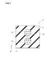
Fig. 1 is a microscopical cross sectional view of a simplified example of a rubber compound. -
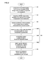
Fig. 2 is a flow chart for explaining a method for analyzing rubber compound as an embodiment of the present invention. -
Fig. 3 is a diagram showing a scanning transmission electron microscope used in the method according to the present invention. -
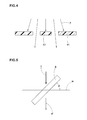
Fig. 4 is a diagram showing a scattering angle limiting aperture for dark-field image. -
Fig. 5 is a diagram for explaining a device for tilting the specimen. -
Fig. 6(a) is a schematic sectional view of the specimen for explaining the position of the focal point, taken along a section including the electron beam axis which is perpendicular to the incidence plane. -
Fig. 6(b) is a schematic sectional view of the specimen for explaining the position of the focal point, taken along a section including the electron beam axis which inclines with respect to the incidence plane. -
Fig. 7 is a schematic sectional view for explaining relationships among the depth of field of a scanning transmission electron microscope, a position of the focal point of the microscope, and the thickness of a specimen. -
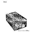
Fig. 8 is a perspective view produced from a dataset of the three-dimensional structure of a rubber compound. -
Fig. 9(a) is a diagram showing a small part of a finite element model of a simplified example of a rubber compound. -
Fig. 9(b) is a closeup thereof. -
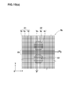
Fig. 10(a) is a diagram for explaining a subdivisional region in the finite element model of a simplified example of a rubber compound. -
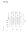
Fig. 10(b) is a closeup thereof. -
Fig. 11 is a perspective view of a three-dimensional finite element model of a simplified example of a rubber compound. -
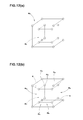
Fig. 12(a) is a diagram showing a three-dimensional regular element of a rubber compound. -
Fig. 12(b) is a diagram showing the one regular element of the subdivisional region is divided into 7 elements. -
Fig. 13 shows slice images at an upper position and a lower position of a specimen of a rubber compound obtained under the after-mentioneddifferent test conditions -
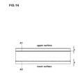
Fig. 14 is a cross sectional view of the specimen for explaining the upper position and lower position referred to inFig. 11 . -
Fig. 15 is a graph showing stress-strain relationships as simulation results and actual measurements. - Embodiments of the present invention will now be described in detail in conjunction with accompanying drawings.
- As shown in
Fig. 1 , the analysis object in this embodiment is a rubber compound (c) which comprises a rubber component (a) as the matrix rubber, and filler particles (b) dispersed in the matrix rubber. As for the suitable method for analyzing the rubber compound (c), the method in this embodiment includes a computerized simulation of the rubber compound (c). - The rubber component (a) can be, for example, natural rubber (NR), isoprene rubber (IR), butyl rubber (IIR), butadiene rubber (BR), styrene butadiene rubber (SBR), styrene isoprene butadiene rubber (SIBR), ethylene-propylene-diene rubber (EPDM), chloroprene rubber (CR), acrylonitrile butadiene rubber (NBR) and the like.
- The filler (b) can be carbon black, silica, clay, talc, magnesium carbonate, magnesium hydroxide and the like of course the rubber component (a) and filler (b) are not limited to these examples. Further, various additives, e.g. sulfur, vulcanization accelerator and the like may be added in the rubber compound (c). In this embodiment, a slice of the rubber compound with a constant thickness (t) is used as a specimen 5 (shown in
Fig. 3 ). - A flow chart implementing the analyzing method as an embodiment of the present invention is shown in
Fig. 2 . This method comprises the following steps S1-S5. - In this step S1, by the use of the scanning transmission electron microscope (STEM) 100, STEM images of the rubber compound (c) are acquired.
- As shown in
Fig.3 , the scanning transmission electron microscope (STEM) 100 comprises: anelectron gun 1 directed perpendicularly to a horizontal plane and capable of emitting electrons downward; a focusinglens 3 for focusing the electrons as anelectron beam 2 on thespecimen 5 of the rubber compound (c);scanning coils 4 including anX-direction scanning coil 4X and a Y-direction scanning coil 4Y for deflecting theelectron beam 2 in the X-direction and Y-direction to scan thespecimen 5; aspecimen holder 6 for holding thespecimen 5; and aspecimen stage 9 on which thespecimen holder 6 is detachably fixed. - In a central portion of the
specimen holder 6, an electron beam pass-throughhole 8 is formed along the central axis (o) of the scanningtransmission electron microscope 100 so thattransmission electrons 7 which penetrate through thespecimen 5 can pass through thehole 8. - In a central portion of the
specimen stage 9, an electron beam pass-throughhole 10 is formed along the central axis (o) and continuously from the electron beam pass-throughhole 8 so that thetransmission electrons 7 can pass through thehole 10. - The
microscope 100 is further provided on the downstream side of thespecimen stage 9 with a scatteringangle limiting aperture 11 in order to limit the passing-through of thetransmission electrons 7. - Further, on the downstream side of the scattering
angle limiting aperture 11, there is disposed adetector 20 for thetransmission electrons 15 passing through theaperture 11. Thedetector 20 comprises ascintillator 13 and aphotoelectron multiplier tube 14. - The
scintillator 13 reemits the energy of theincident electrons 12 passing though theaperture 11, in the form of light. - The
photoelectron multiplier tube 14 converts the incident light from thescintillator 13 to an electronic signal. Incidentally, the above-mentionedspecimen stage 9, scatteringangle limiting aperture 11,scintillator 13 andphotoelectron multiplier tube 14 are arranged in a specimen room of a casing main body (not shown) of themicroscope system 100. - The
microscope 100 is used to acquire STEM images of the rubber compound (c) as follows. First, thespecimen holder 6 with thespecimen 5 is attached to thespecimen stage 9 by an operating personnel. - Next, the
electron beam 2 emitted from theelectron gun 1 and accelerated by an accelerator (not shown) and focused by the focusinglens 3 is scanned on thespecimen 5 by the X-direction and Y-direction scanning coils electrons 7, which penetrate through thespecimen 5 with or without scattered, go out from the lower surface of thespecimen 5. - The
outgoing electrons 7 travel through theholes angle limiting aperture 11 which allows the electrons having particular scattering angles to pass through it. - The
electrons 12 passing through the scatteringangle limiting aperture 11 go into thescintillator 13, and thereby the energy of theincident electrons 12 is reemitted in the form of light. Then by the accompanyingphotoelectron multiplier tube 14, the light is converted to an electronic signal. The electrical signal is amplified and converted to digital data by an amplifier and A/D converter (not shown). The digital data are transmitted to a display (not shown) in which, according to the transmitted signal, brightness modulation is made, and an electron beam transmission image reflecting the internal structure of thespecimen 5 is displayed as a STEM image, and at the same time, the digital data are stored in a memory of the computer. Thus, a plurality of STEM images corresponding to the scan positions are acquired as the STEM images' dataset. - The intensity and scattering angle of the
outgoing electrons 7 are varied depending on the internal state, thickness and/or atomic species of thespecimen 5. The scattering angle is also varied by the accelerating voltage. For example, if the accelerating voltage is decreased, the electrons are scattered more in thespecimen 5, and the scattering angle or outgoing angle from the lower surface of thespecimen 5 with respect to the central axis (o) is increased. - As shown in
Fig. 4 , the scatteringangle limiting aperture 11 may be provided in its center with a masking shield 17 for further limiting the passing of theelectrons 7 although the example shown inFig. 3 is not provided with such masking shield. In general, the electron beam transmission image becomes a bright-field image when the additional masking shield is not used, but it becomes a dark-field image if the masking shield is used, - In order to create a clear image, the camera length L1 namely the distance between the
specimen 5 and thescintillator 13 is preferably set in a range of from 8 to 150 cm. - The accelerating voltage for the electron beam may be set in a range of 100 to 3000 kv depending on the
specimen 5. - In the STEM image acquiring step S1 in this embodiment, a plurality of images of the rubber compound (c) are took from different angles with respect to the central axis (o) of the scanning
transmission electron microscope 100. For this purpose, themicroscope 100 is provided with a specimen tilting device (not shown) to tilt thespecimen 5 with respect to the central axis (o) with this, as shown inFig. 5 , thespecimen 5 can be held at different tilt angles θ with respect to a horizontal plane H. In this embodiment, the computer outputs a control signal to the specimen tilting device and according thereto the device tilts thespecimen 5 at a specific angle θ. - The variable range of the tilt angle θ of the
specimen 5 is -90 to +90 degrees, preferably -70 to +70 degrees. However, if the specimen is a round bar of the rubber compound, the variable range of the angle θ may be -180 to +180 degrees. - Firstly, the
specimen 5 is tilted at a measuring start angle θ and in this tilted state, the STEM images or the dataset thereof are acquired as explained above. Then, until a measuring stop angle θ, the process of changing the tilt angle of thespecimen 5 and acquiring the dataset of the STEM images of thespecimen 5 at that tilt angle are repeated at a step in a range of from 0.5 to 4 degrees, preferably 1 to 2 degrees in order to obtain the after-mentioned slice images clearly and efficiently. - Thereby, the dataset of the STEM images of the specimen inclined at different tilt angles are obtained. Incidentally, the measuring start angle θ and measuring stop angle θ can be arbitrarily set on the microscope by using a controller. In this embodiment, the measuring start angle θ is +70 degrees, and the measuring stop angle θ is -70 degrees.
- In this embodiment, the focal point F of the electron beam (e) is set in a thickness center region C of the
specimen 5 as shown inFig. 6(a) . - when the focal point F of the electron beam (e) is set at the
upper surface 5a of thespecimen 5, as shown inFig.7 , there is a possibility that a clear image cannot be obtained in the vicinity of thelower surface 5b of thespecimen 5. For instance, as shown inFig. 7 , if the thickness (t) of thespecimen 5 is 1000 nm, the depth (f) of field of the microscope is 1200 nm (or +/-600 nm), and the focal point F is set at thesurface 5a of thespecimen 5, then a lower part B having 400 nm thickness of thespecimen 5 is outside the depth of field, and accordingly, a clear image of such part B can not be obtained. This problem is liable to occur with increase in the thickness (t). - on the other hand, when the focal point F of the electron beam (e) is set in the thickness center region C of the
specimen 5 as shown inFig. 6(a) , the range on thespecimen 5 in which a clear image can be obtained becomes increased. It is desirable that the depth (f) of field can completely overlaps or encompass the thickness (t) of thespecimen 5. - In
Fig. 6(a) , theupper surface 5a and thelower surface 5b of thespecimen 5 are perpendicular to the electron beam axis (namely, the incidence angle is equal to 90 deg.). InFig. 6(b) , theupper surface 5a and thelower surface 5b of thespecimen 5 are inclined with respect to the electron beam axis (namely, the incidence angle is not equal to 90 deg.). Under such inclined state, the thickness of thespecimen 5 measured along the electron beam axis is referred to as apparent thickness (t') in contrast to the real thickness (t) measured perpendicularly to theupper surface 5a. - From the real thickness (t), the tilt angle θ of the
specimen 5, and the apparent thickness (t') can be obtained as follows:
- Here, θ is the tilt angle of the
specimen 5 with respect to the horizontal plane, as shown inFig. 6(b) . - It is desirable that the central region C within which the focal point F is set, ranges 30 %, preferably 20 %, more preferably 10 % of the real/apparent thickness. The central region C may be off-centered, but preferably it is centered on the center of the real/apparent thickness.
- The real thickness (t) may be less than 200 nm as usual, but it is preferably set in a range of from 200 to 1500 nm, more preferably 500 to 1000 nm. By increasing the thickness (t) near to 1500 nm, the dispersion of the filler particles including a compact cluster having a diameter of 200 nm or more can be accurately simulated. Incidentally, the focal point F is adjusted by the focusing
lens 3 and/orspecimen stage 9 by the use of a focal point adjuster of themicroscope system 100. - In this step S2, from the dataset of the STEM images acquired in the step S1, a three-dimensional structure of the rubber compound is reconstructed as numerical data (hereinafter the "3D dataset") by executing a tomographic method with the computer, and the 3D dataset is stored in a memory of the computer.
- As the dataset of the STEM images, those acquired by changing the tilt angle of the
specimen 5 as explained above can be preferably used. But, it is also possible to use those acquired by not changing the tilt angle, namely acquired at a single tilt angle of thespecimen 5 preferably zero degree with respect to the horizontal plane. - From the 3D dataset, the computer can create and output various images as visual information as well as numerical data.
Fig. 8 shows such created image which is a perspective view of the filler particles dispersed in the rubber compound. - In this step S3, from the reconstructed 3D dataset of the three-dimensional structure of the rubber compound, slice images of the rubber compound (c) taken along predetermined sections of the rubber compound (c) are reconstructed by the computer as numerical data (herein after the "slice image dataset"), and the slice image dataset is stored in a memory of the computer. The above-mentioned predetermined sections of the rubber compound can be arbitrarily determined according to the coordinate system (Cartesian or polar or cylindrical) employed in the subsequent step S4.
- In this step S4, a finite element model of the rubber compound (c) is generated based on the slice image of the rubber compound (c). Step S4 further comprises a first step S41, a second step S42 and a third step S43.
- In the first step S41, a first
finite element model 5a of the rubber compound is set using only regular elements each with the same shape, as shown inFig. 9(a) . In this step S41, the slice image is subjected to an image processing to divide the entire region of the slice image into a domain of the rubber component (a), a domain of the filler particle (b) and/or a domain of other component if any. As to the image processing method, a known method can be used in which, based on threshold levels of gray level, micro regions of the slice image are each identified whether it is a rubber domain or a filler domain (or other domain if any). - Next, at least one slice image including at least two domains of the rubber component (a) and filler particles (b) is divided by using only regular elements eb each with the same shape, to generate a first finite element model of the rubber compound (c).
-
Fig. 9(a) shows a small part of the firstfinite element model 5a taken along a corresponding slice image of a simplified example of the rubber compound (c), andFig. 9(b) shows a closeup thereof. As shown inFig. 9(b) , each regular element eb is defined as a mesh on a regular grid with boundary GD (L1 and L2) at even pitches P in the x-axis direction, y-axis direction. In this embodiment, each regular element eb has a square shape with four node points (n) which are located on intersections between lines L1 and L2. - As shown in
Fig. 9(a) , the firstfinite element model 5a of the rubber compound comprises adomain 21 of the rubber component and a plurality ofdomains 22 of the filler particles. In this embodiment, shadowed areas indicate thefiller particle domains 22. - In the
filler particle domain 22, the filler particle is discretized into a finite number of regular elements eb. In therubber component domain 21, the rubber component is also discretized into a finite number of regular elements eb. - In the discretization process, for example, with the computer, the regular grid is defined and superimposed onto the image-processed slice image or images, and for each regular element eb of the grid, it is computed which one of the rubber component and filler particle has the highest proportion of area or volume in the concerned regular element eb. Then, the regular element eb is defined as being one with the highest proportion. Namely, the computer determines whether each regular element eb belongs to the rubber component or the filler particle. By employing a structured regular grid and regular elements, it is possible to generate the
rubber compound model 5a rapidly. Further, since the discretization process of the rubber compound is based on the slice image or images accurately created from the 3D dataset of the rubber compound, a precise model of the rubber compound can be obtained. - Also, information is defined on each regular element eb, which is required for simulations or numerical analysis conducted by the use of a numerical analysis method, e.g. a finite element method or the like. Such information includes at least indexes and coordinate values of node points (n) of each regular element eb.
- Further, on each element eb, material characteristics (materials properties) of the part of the rubber compound which part is represented by the concerned element are defined. Specifically, on each of the elements eb of the
rubber component domain 21 andfiller particle domains 22, material constants corresponding to physical properties of the rubber component or filler are defined and stored in a memory of the computer as numerical data. - Next, in the second step S42, a
subdivisional region 23 is determined in the firstfinite element model 5a at least partially. - The
subdivisional region 23 is a region where small elements smaller than regular elements should be employed to make it possible to research the deformation behavior thereof in more detail. By using thesubdivisional region 23 in the firstfinite element model 5a at least partially, accurate computation results may be obtained therefrom. In view of above, thesubdivisional region 23 is preferably determined on the location where accurate computation results are required. - As shown in
Fig. 1 , in the rubber compound c with filler particles, a large strain and stress especially tend to be generated in the rubber part b1 between two filler particles b. In this embodiment, thesubdivisional region 23 is determined as the region including the rubber part b1 at least partially. - The scope of the
subdivisional region 23 may be designated by an operating personnel using input devices such as the keyboards or the mouse. In order to identify which regular elements have been designated for the subdivisional region, information is added to the memory in thecomputer 1. - Further, the
subdivisional region 23 may be determined as follows: - Firstly, by using the first
finite element model 5a of the rubber compound, a simulation of deformation of the rubber compound is carried out under given conditions; - Next, a large deformed region where the largest strain or stress is generated in the first
finite element model 5a is determined based on the simulation results; and - Finally, the
subdivisional region 23 is determined as the region which includes the large deformed region at least partially. - In the third step S43, each regular element included in the
subdivisional region 23 is divided into two or more elements to generate thefinite element model 5b (shown inFig. 10(a) ) of the rubber compound is carried out. In the third step S43, pitches P of longitudinal lines L1 and/or lateral lines L2 on the regular grid passing through thesubdivisional region 23 are changed so that each regular element eb included in thesubdivisional region 23 changes small. - As shown in
Fig. 10(b) , pitches of the lateral lines L2 passing through thesubdivisional region 23 is changed into a half of initial pitch given as the firstfinite element model 5a of the rubber compound (c), although the pitches of the longitudinal lines L1 is not changed, in this embodiment with this, each regular element eb of therubber domain 21 between thefiller domains 22 is divided into two equal elements as to the y-axis direction. Namely, each regular elements eb in thesubdivisional region 23 is divided into the small element es which is a rectangular shape with the same length of x-axis direction and a half length of y-axis compared to the initial regular element eb. - Various ratios for changing the initial pitch P between lines L1 and/or L2 of the regular grid can be employed to make the small elements es in the
subdivisional region 23, the ratio is not limited as 0.5. Moreover, the subdividing process may be repeated frequently until necessary resolution for thesubdivisional region 23 is obtained. - In this step S5, using the
finite element model 5b of the rubber compound, a simulation of deformation of the rubber compound is carried out under given conditions. For this purpose, a known method, e.g. homogeneization method (asymptotic expansion homogeneization method) or the like can be employed. - In this embodiment, using one slice image, a two-dimensional
finite element model 5b can be generated. As shown inFig. 11 , however, a three-dimensionalfinite element model 5c can be generated Using a plurality of slice images. In this three-dimensionalfinite element model 5c, rectangular solid elements may be employed as the regular elements eb. As shown inFigs. 12(a) and 12(b) , for example, the subdividing process to the three-dimensionalfinite element model 5c may be done as follows: - As shown in
Fig. 12(a) , a small element es of a rectangular solid shape smaller than the regular element eb is defined within each regular element eb of a rectangular solid shape in thesubdivisional region 23 so that each center of gravities thereof coincides each other: and - Next, as shown in
Fig. 12(b) , each node point ns of the small elements eb is associated with each corresponding node point nb of the regular elements es using a beam (s). - With this, the regular elements eb is divided into one small center element es having the rectangular solid shape, and six elements (ea) having quadrangular pyramid shapes surrounding the center element es.
- The present invention is more specifically described and explained by means of the following Examples and References. It is to be understood that the present invention is not limited to these Examples.
- In order to confirm the advantage of the method according to the invention, comparison tests were conducted.
- Firstly, an explanation is given about the STEM image acquiring step S1 and three-dimensional structure reconstruction step S2. Equipments and materials used are as follows.
- JEOL Ltd. JEM-2100F
- Leica Ultramicrotome EM UC6
- 100 parts by mass of SBR (Sumitomo Chemical Company, Limited: SBR1502)
- 53.2 parts by mass of silica (Rhodia Japan Ltd.: 115Gr)
- 4.4 parts by mass of silane coupling agent (Si69)
- 0.5 parts by mass of sulfur (Tsurumi Chemical. Co. Ltd.: Powdered sulfur)
- 1 parts by mass of vulcanization accelerator A (Ouchi Shinko Chemical Industrial Co., Ltd.: NOCCELER NS)
- 1 parts by mass of vulcanization accelerator B (Ouchi Shinko Chemical Industrial Co., Ltd.: NOCCELER D)
- Using a banbury mixer, the materials except for the sulfur and vulcanization accelerators were kneaded for four minutes at 160 degrees C. Then, the kneaded materials to which the sulfur and vulcanization accelerators were added was further kneaded by the use of a open roll kneader for two minutes at 100 degrees C, and a raw rubber compound was prepared. The raw rubber compound was vulcanized for thirty minutes at 175 degrees C.
- The vulcanized rubber was sliced by using the ultramicrotome, and a specimen with a thickness of 500 nm was prepared.
- Using the STEM mode (camera length L1= 150 cm, accelerating voltage = 200 kv) of the microscope JEM-2100F, STEM images of the specimen were acquired by changing the tilt angle of the specimen from -60 to +60 degrees at a step of 1 degree, wherein, in the case of
test condition 1, the focal point was set at the thickness center of the specimen, and in the case oftest condition 2, the focal point was set at the upper surface of the specimen. - From the data of the STEM images obtained under each test condition, a 3D dataset of a three-dimensional structure of the rubber compound was reconstructed.
-
Fig. 13 shows slice images at the upper position A1 and lower position A2 of each of three-dimensional structures created from the 3D dataset. The upper and lower positions A1 and A2 are at 40 nm from the upper and lower surfaces, respectively, as shown inFig. 14 . As shown, in thetest condition 2, the image at the lower position became unclear. However, in thetest condition 1, the image at the lower position as well as the image at the upper position became clear. Also, the above-mentioned perspective view shown inFig. 8 was created from the 3D dataset obtained under thetest condition 1. - Based on the slice image at the lower position A2 obtained in the
test condition 1, two kinds of two-dimensional rubber compound models were defined as Examples 1 and 2. More specifically, the Example 1 was defined using only regular elements each having square shape. Example 2 was defined using regular elements having square shape, and small elements which were defined between a pair of filler particle domains. Each small element had a length of y-axis direction being a half of that of the regular element, and a length of x-axis direction being the same of the regular element. - Then, using these rubber compound models, a simulation for tensile deformation was carried out to obtain the stress-strain relationship under the following conditions.
- Maximum tensile strain: 3 mm
- Tensile strain rate: 100 mm/min
- Macroscopic region; 20
mm X 20 mm - The simulation results are shown in
Fig. 15 together with the actual measurements obtained from the rubber compound. As shown inFig. 15 , the simulation result according to Example 2 has a high correlation with the actual measurements.
Claims (7)
- A method for analyzing rubber compound including a rubber component and filler particles, comprising:a STEM image acquiring step in which, by the use of a scanning transmission electron microscope (STEM), data of STEM images of the rubber compound are acquired; anda researching step for researching the STEM images or secondary information based on the originally data of STEM images; whereinin the STEM image acquiring step, the focal point of the scanning transmission electron microscope is set in a thickness center region of a specimen of the rubber compound.
- The method according to claim 1, wherein
in the STEM image acquiring step, the specimen of the rubber compound is tilted with respect to the central axis of the scanning transmission electron microscope and the STEM images are took at different tilt angles of the specimen of the rubber compound, and
the researching step comprises a three-dimensional structure reconstruction step in which, based on the data of the STEM images, a dataset of a three-dimensional structure of the rubber compound is reconstructed. - The method according to claim 1 or 2, wherein
the focal point of the scanning transmission electron microscope is set in a thickness center region of the specimen of the rubber compound based on an apparent thickness measured along the direction of the electron beam axis across the specimen of the rubber compound. - The method according to claim 1 or 2, wherein
the thickness of the specimen of the rubber compound is 200 to 1500 nm. - The method according to claim 1 or 2, wherein
a distance between the specimen of the rubber compound and a detector for the transmission electrons of the scanning transmission electron microscope is 8 to 150 cm. - The method according to claim 2, wherein
the researching step further comprises:a finite element model generating step in which, based on the dataset of the three-dimensional structure of the rubber compound, a finite element model of the rubber compound is generated, so that the finite element model comprises a domain of the rubber component divided into a finite number of elements, and domains of the filler particles each divided into a finite number of elements; anda simulation step in which, based on the finite element model, a simulation of deformation of the rubber compound is carried out. - The method according to claim 6, wherein
the finite element model generating step comprises:a first step in which a first finite element model of the rubber compound is set using only regular elements each with the same shape;a second step in which a subdivisionalal region is determined in the first finite element model at least partially; anda third step in which each element of the subdivisional region is divided into two or more elements to generate the finite element model of the rubber compound.
Applications Claiming Priority (3)
| Application Number | Priority Date | Filing Date | Title |
|---|---|---|---|
| JP2011181812A JP2013044607A (en) | 2011-08-23 | 2011-08-23 | Method of observing rubber material |
| JP2011193098A JP2013054578A (en) | 2011-09-05 | 2011-09-05 | Method for simulating rubber material |
| JP2011200983A JP5767541B2 (en) | 2011-09-14 | 2011-09-14 | Rubber material simulation method |
Publications (2)
| Publication Number | Publication Date |
|---|---|
| EP2562534A2 true EP2562534A2 (en) | 2013-02-27 |
| EP2562534A3 EP2562534A3 (en) | 2014-05-21 |
Family
ID=46466345
Family Applications (1)
| Application Number | Title | Priority Date | Filing Date |
|---|---|---|---|
| EP12175905.4A Withdrawn EP2562534A3 (en) | 2011-08-23 | 2012-07-11 | Method for analyzing rubber compound with filler particles |
Country Status (3)
| Country | Link |
|---|---|
| US (1) | US20130051656A1 (en) |
| EP (1) | EP2562534A3 (en) |
| CN (1) | CN102954975A (en) |
Families Citing this family (8)
| Publication number | Priority date | Publication date | Assignee | Title |
|---|---|---|---|---|
| JP5395864B2 (en) * | 2011-09-14 | 2014-01-22 | 住友ゴム工業株式会社 | Rubber material simulation method |
| JP6239246B2 (en) | 2013-03-13 | 2017-11-29 | 株式会社日立ハイテクノロジーズ | Charged particle beam apparatus, sample observation method, sample stage, observation system, and light emitting member |
| JP5913260B2 (en) * | 2013-11-14 | 2016-04-27 | 住友ゴム工業株式会社 | Method for simulating polymer materials |
| EP2882203A1 (en) | 2013-12-06 | 2015-06-10 | Oticon A/s | Hearing aid device for hands free communication |
| CN105419003B (en) * | 2015-12-25 | 2017-08-11 | 贵州大学 | The method that fast slowdown monitoring latex coprecipitation method prepares the coprecipitated behavior of NR/CB composites |
| CN107505480B (en) * | 2017-08-16 | 2020-05-08 | 四川理工学院 | A method for detecting the dispersion of fillers in rubber composite materials |
| CN109916941B (en) * | 2019-03-25 | 2021-04-30 | 苏州大学 | 3D printing separation detection method for premixed powder |
| CN114923752B (en) * | 2022-05-17 | 2025-05-06 | 中国电子产品可靠性与环境试验研究所((工业和信息化部电子第五研究所)(中国赛宝实验室)) | A method for identifying silicone adhesive filler |
Family Cites Families (12)
| Publication number | Priority date | Publication date | Assignee | Title |
|---|---|---|---|---|
| US6458883B1 (en) * | 1999-01-14 | 2002-10-01 | Jsr Corporation | Conductive rubber composition and manufacturing method and conductive rubber member thereof |
| US7907765B2 (en) * | 2001-03-28 | 2011-03-15 | University Of Washington | Focal plane tracking for optical microtomography |
| JP3995926B2 (en) * | 2001-09-18 | 2007-10-24 | 株式会社富士通長野システムエンジニアリング | Structure analysis program, structure analysis method, structure analysis apparatus, and semiconductor integrated circuit manufacturing method |
| WO2004035688A1 (en) * | 2002-10-03 | 2004-04-29 | Sekisui Chemical Co., Ltd. | Thermoplastic saturated norbornene based resin film, ans method for producing thermoplastic saturated norbornene based resin film |
| EP2063450A1 (en) * | 2007-11-21 | 2009-05-27 | FEI Company | Method for obtaining a scanning transmission image of a sample in a particle-optical apparatus |
| JP5324820B2 (en) * | 2008-05-19 | 2013-10-23 | 住友ゴム工業株式会社 | How to create an analysis model |
| JP2010091330A (en) * | 2008-10-06 | 2010-04-22 | Sumitomo Chemical Co Ltd | Method and system for analyzing orientation function |
| JP4603082B2 (en) * | 2009-02-03 | 2010-12-22 | 株式会社ブリヂストン | Rubber material deformation behavior prediction apparatus and rubber material deformation behavior prediction method |
| JP2010181342A (en) * | 2009-02-06 | 2010-08-19 | Bridgestone Corp | Device and method for estimating deformation behavior of rubber material |
| CN101672810B (en) * | 2009-09-14 | 2011-06-08 | 哈尔滨飞机工业集团有限责任公司 | Method for analyzing composition uniformity of rubber material |
| JP5269732B2 (en) * | 2009-09-28 | 2013-08-21 | 株式会社ブリヂストン | Method for predicting deformation behavior of rubber material and apparatus used therefor |
| JP5767477B2 (en) * | 2011-01-14 | 2015-08-19 | 住友ゴム工業株式会社 | How to observe rubber materials |
-
2012
- 2012-07-11 US US13/546,183 patent/US20130051656A1/en not_active Abandoned
- 2012-07-11 EP EP12175905.4A patent/EP2562534A3/en not_active Withdrawn
- 2012-07-18 CN CN2012102494115A patent/CN102954975A/en active Pending
Non-Patent Citations (1)
| Title |
|---|
| None |
Also Published As
| Publication number | Publication date |
|---|---|
| EP2562534A3 (en) | 2014-05-21 |
| CN102954975A (en) | 2013-03-06 |
| US20130051656A1 (en) | 2013-02-28 |
Similar Documents
| Publication | Publication Date | Title |
|---|---|---|
| US20130051656A1 (en) | Method for analyzing rubber compound with filler particles | |
| US20140324401A1 (en) | Method for simulating rubber material | |
| EP2568284A2 (en) | Method for simulating deformation of rubber compound with filler particles | |
| JP2023166550A (en) | Scatter correction for computed tomography imaging | |
| EP2570808B1 (en) | Method for simulating deformation of rubber compound | |
| JP5187810B2 (en) | Film thickness measuring method and sample preparation method, film thickness measuring apparatus and sample preparation apparatus | |
| JP2013054578A (en) | Method for simulating rubber material | |
| US20160283624A1 (en) | Simulation method for polymer material | |
| Postek et al. | Modeling for accurate dimensional scanning electron microscope metrology: Then and now | |
| JP5767541B2 (en) | Rubber material simulation method | |
| DE102019201069A1 (en) | Method for determining a specimen orientation for a 2D X-ray system | |
| US10690593B2 (en) | Sample analyzer and recording medium recording sample analysis program | |
| US20220113265A1 (en) | Scatter correction for computed tomography imaging | |
| JP7359660B2 (en) | Deformation analysis method for rubber materials | |
| JP6904890B2 (en) | Fracture cause estimation method and estimation system, and stress level estimation method and estimation system | |
| Turner | Erosion and dilation of edges in dimensional X-ray computed tomography images | |
| JP2020119686A (en) | Electron microscope and depth calculation method for three-dimensional structure | |
| Abdelrehim | Development of a Creep Cavitation-Based Model Incorporating Partial Coalescence for Lifetime Prediction. | |
| EP3602021A1 (en) | Method and apparatus for determining at least two transmission positions | |
| Gray et al. | Optimizing Compton back scattering parameters using a simulation code | |
| Henschel et al. | „Application of focal curves for X-Ray microdiffraction methods “ | |
| Tillotson | Assessing Lamellae Thickness During Fib Milling with Monte Carlo Modelling | |
| WO2025258055A1 (en) | Internal shape evaluation system and internal shape evaluation method | |
| JP2024156329A (en) | Method for determining the composition and structure of crystal grains in rubber-metal compounds | |
| Wang et al. | APPLICATION OF STATISTICAL METHODS FOR ASSESSMENT OF COMPONENTS OF VARIANCE IN PROBABILITY OF DETECTION MODELS |
Legal Events
| Date | Code | Title | Description |
|---|---|---|---|
| PUAI | Public reference made under article 153(3) epc to a published international application that has entered the european phase |
Free format text: ORIGINAL CODE: 0009012 |
|
| AK | Designated contracting states |
Kind code of ref document: A2 Designated state(s): AL AT BE BG CH CY CZ DE DK EE ES FI FR GB GR HR HU IE IS IT LI LT LU LV MC MK MT NL NO PL PT RO RS SE SI SK SM TR |
|
| AX | Request for extension of the european patent |
Extension state: BA ME |
|
| PUAL | Search report despatched |
Free format text: ORIGINAL CODE: 0009013 |
|
| RIC1 | Information provided on ipc code assigned before grant |
Ipc: G01N 23/18 20060101AFI20140410BHEP |
|
| AK | Designated contracting states |
Kind code of ref document: A3 Designated state(s): AL AT BE BG CH CY CZ DE DK EE ES FI FR GB GR HR HU IE IS IT LI LT LU LV MC MK MT NL NO PL PT RO RS SE SI SK SM TR |
|
| AX | Request for extension of the european patent |
Extension state: BA ME |
|
| STAA | Information on the status of an ep patent application or granted ep patent |
Free format text: STATUS: THE APPLICATION IS DEEMED TO BE WITHDRAWN |
|
| 18D | Application deemed to be withdrawn |
Effective date: 20141122 |