EP2561675B1 - Bildsensor und verfahren zur herstellung eines bildsensors - Google Patents
Bildsensor und verfahren zur herstellung eines bildsensors Download PDFInfo
- Publication number
- EP2561675B1 EP2561675B1 EP11816721.2A EP11816721A EP2561675B1 EP 2561675 B1 EP2561675 B1 EP 2561675B1 EP 11816721 A EP11816721 A EP 11816721A EP 2561675 B1 EP2561675 B1 EP 2561675B1
- Authority
- EP
- European Patent Office
- Prior art keywords
- collimator
- layer
- solid state
- sensor
- image sensor
- Prior art date
- Legal status (The legal status is an assumption and is not a legal conclusion. Google has not performed a legal analysis and makes no representation as to the accuracy of the status listed.)
- Not-in-force
Links
Images


Classifications
-
- B—PERFORMING OPERATIONS; TRANSPORTING
- B23—MACHINE TOOLS; METAL-WORKING NOT OTHERWISE PROVIDED FOR
- B23K—SOLDERING OR UNSOLDERING; WELDING; CLADDING OR PLATING BY SOLDERING OR WELDING; CUTTING BY APPLYING HEAT LOCALLY, e.g. FLAME CUTTING; WORKING BY LASER BEAM
- B23K1/00—Soldering, e.g. brazing, or unsoldering
- B23K1/0008—Soldering, e.g. brazing, or unsoldering specially adapted for particular articles or work
- B23K1/0016—Soldering of electronic components
-
- H—ELECTRICITY
- H04—ELECTRIC COMMUNICATION TECHNIQUE
- H04N—PICTORIAL COMMUNICATION, e.g. TELEVISION
- H04N25/00—Circuitry of solid-state image sensors [SSIS]; Control thereof
-
- B—PERFORMING OPERATIONS; TRANSPORTING
- B23—MACHINE TOOLS; METAL-WORKING NOT OTHERWISE PROVIDED FOR
- B23K—SOLDERING OR UNSOLDERING; WELDING; CLADDING OR PLATING BY SOLDERING OR WELDING; CUTTING BY APPLYING HEAT LOCALLY, e.g. FLAME CUTTING; WORKING BY LASER BEAM
- B23K1/00—Soldering, e.g. brazing, or unsoldering
- B23K1/19—Soldering, e.g. brazing, or unsoldering taking account of the properties of the materials to be soldered
-
- B—PERFORMING OPERATIONS; TRANSPORTING
- B23—MACHINE TOOLS; METAL-WORKING NOT OTHERWISE PROVIDED FOR
- B23K—SOLDERING OR UNSOLDERING; WELDING; CLADDING OR PLATING BY SOLDERING OR WELDING; CUTTING BY APPLYING HEAT LOCALLY, e.g. FLAME CUTTING; WORKING BY LASER BEAM
- B23K1/00—Soldering, e.g. brazing, or unsoldering
- B23K1/20—Preliminary treatment of work or areas to be soldered, e.g. in respect of a galvanic coating
-
- B—PERFORMING OPERATIONS; TRANSPORTING
- B29—WORKING OF PLASTICS; WORKING OF SUBSTANCES IN A PLASTIC STATE IN GENERAL
- B29C—SHAPING OR JOINING OF PLASTICS; SHAPING OF MATERIAL IN A PLASTIC STATE, NOT OTHERWISE PROVIDED FOR; AFTER-TREATMENT OF THE SHAPED PRODUCTS, e.g. REPAIRING
- B29C65/00—Joining or sealing of preformed parts, e.g. welding of plastics materials; Apparatus therefor
- B29C65/48—Joining or sealing of preformed parts, e.g. welding of plastics materials; Apparatus therefor using adhesives, i.e. using supplementary joining material; solvent bonding
- B29C65/52—Joining or sealing of preformed parts, e.g. welding of plastics materials; Apparatus therefor using adhesives, i.e. using supplementary joining material; solvent bonding characterised by the way of applying the adhesive
-
- H—ELECTRICITY
- H10—SEMICONDUCTOR DEVICES; ELECTRIC SOLID-STATE DEVICES NOT OTHERWISE PROVIDED FOR
- H10F—INORGANIC SEMICONDUCTOR DEVICES SENSITIVE TO INFRARED RADIATION, LIGHT, ELECTROMAGNETIC RADIATION OF SHORTER WAVELENGTH OR CORPUSCULAR RADIATION
- H10F39/00—Integrated devices, or assemblies of multiple devices, comprising at least one element covered by group H10F30/00, e.g. radiation detectors comprising photodiode arrays
- H10F39/011—Manufacture or treatment of image sensors covered by group H10F39/12
- H10F39/014—Manufacture or treatment of image sensors covered by group H10F39/12 of CMOS image sensors
-
- H—ELECTRICITY
- H10—SEMICONDUCTOR DEVICES; ELECTRIC SOLID-STATE DEVICES NOT OTHERWISE PROVIDED FOR
- H10F—INORGANIC SEMICONDUCTOR DEVICES SENSITIVE TO INFRARED RADIATION, LIGHT, ELECTROMAGNETIC RADIATION OF SHORTER WAVELENGTH OR CORPUSCULAR RADIATION
- H10F39/00—Integrated devices, or assemblies of multiple devices, comprising at least one element covered by group H10F30/00, e.g. radiation detectors comprising photodiode arrays
- H10F39/011—Manufacture or treatment of image sensors covered by group H10F39/12
- H10F39/024—Manufacture or treatment of image sensors covered by group H10F39/12 of coatings or optical elements
-
- H—ELECTRICITY
- H10—SEMICONDUCTOR DEVICES; ELECTRIC SOLID-STATE DEVICES NOT OTHERWISE PROVIDED FOR
- H10F—INORGANIC SEMICONDUCTOR DEVICES SENSITIVE TO INFRARED RADIATION, LIGHT, ELECTROMAGNETIC RADIATION OF SHORTER WAVELENGTH OR CORPUSCULAR RADIATION
- H10F39/00—Integrated devices, or assemblies of multiple devices, comprising at least one element covered by group H10F30/00, e.g. radiation detectors comprising photodiode arrays
- H10F39/10—Integrated devices
- H10F39/12—Image sensors
- H10F39/18—Complementary metal-oxide-semiconductor [CMOS] image sensors; Photodiode array image sensors
-
- H—ELECTRICITY
- H10—SEMICONDUCTOR DEVICES; ELECTRIC SOLID-STATE DEVICES NOT OTHERWISE PROVIDED FOR
- H10F—INORGANIC SEMICONDUCTOR DEVICES SENSITIVE TO INFRARED RADIATION, LIGHT, ELECTROMAGNETIC RADIATION OF SHORTER WAVELENGTH OR CORPUSCULAR RADIATION
- H10F39/00—Integrated devices, or assemblies of multiple devices, comprising at least one element covered by group H10F30/00, e.g. radiation detectors comprising photodiode arrays
- H10F39/80—Constructional details of image sensors
- H10F39/802—Geometry or disposition of elements in pixels, e.g. address-lines or gate electrodes
-
- H—ELECTRICITY
- H10—SEMICONDUCTOR DEVICES; ELECTRIC SOLID-STATE DEVICES NOT OTHERWISE PROVIDED FOR
- H10F—INORGANIC SEMICONDUCTOR DEVICES SENSITIVE TO INFRARED RADIATION, LIGHT, ELECTROMAGNETIC RADIATION OF SHORTER WAVELENGTH OR CORPUSCULAR RADIATION
- H10F39/00—Integrated devices, or assemblies of multiple devices, comprising at least one element covered by group H10F30/00, e.g. radiation detectors comprising photodiode arrays
- H10F39/80—Constructional details of image sensors
- H10F39/806—Optical elements or arrangements associated with the image sensors
-
- B—PERFORMING OPERATIONS; TRANSPORTING
- B23—MACHINE TOOLS; METAL-WORKING NOT OTHERWISE PROVIDED FOR
- B23K—SOLDERING OR UNSOLDERING; WELDING; CLADDING OR PLATING BY SOLDERING OR WELDING; CUTTING BY APPLYING HEAT LOCALLY, e.g. FLAME CUTTING; WORKING BY LASER BEAM
- B23K2101/00—Articles made by soldering, welding or cutting
- B23K2101/36—Electric or electronic devices
- B23K2101/42—Printed circuits
-
- B—PERFORMING OPERATIONS; TRANSPORTING
- B23—MACHINE TOOLS; METAL-WORKING NOT OTHERWISE PROVIDED FOR
- B23K—SOLDERING OR UNSOLDERING; WELDING; CLADDING OR PLATING BY SOLDERING OR WELDING; CUTTING BY APPLYING HEAT LOCALLY, e.g. FLAME CUTTING; WORKING BY LASER BEAM
- B23K2103/00—Materials to be soldered, welded or cut
- B23K2103/50—Inorganic materials other than metals or composite materials
-
- H—ELECTRICITY
- H10—SEMICONDUCTOR DEVICES; ELECTRIC SOLID-STATE DEVICES NOT OTHERWISE PROVIDED FOR
- H10F—INORGANIC SEMICONDUCTOR DEVICES SENSITIVE TO INFRARED RADIATION, LIGHT, ELECTROMAGNETIC RADIATION OF SHORTER WAVELENGTH OR CORPUSCULAR RADIATION
- H10F39/00—Integrated devices, or assemblies of multiple devices, comprising at least one element covered by group H10F30/00, e.g. radiation detectors comprising photodiode arrays
- H10F39/80—Constructional details of image sensors
- H10F39/804—Containers or encapsulations
-
- Y—GENERAL TAGGING OF NEW TECHNOLOGICAL DEVELOPMENTS; GENERAL TAGGING OF CROSS-SECTIONAL TECHNOLOGIES SPANNING OVER SEVERAL SECTIONS OF THE IPC; TECHNICAL SUBJECTS COVERED BY FORMER USPC CROSS-REFERENCE ART COLLECTIONS [XRACs] AND DIGESTS
- Y10—TECHNICAL SUBJECTS COVERED BY FORMER USPC
- Y10T—TECHNICAL SUBJECTS COVERED BY FORMER US CLASSIFICATION
- Y10T156/00—Adhesive bonding and miscellaneous chemical manufacture
- Y10T156/10—Methods of surface bonding and/or assembly therefor
Definitions
- This invention relates to the field of bonding a collimator to an imager and, in particular, to using catch pads throughout the imaged area, and more particularly to an image sensor and a method of making an image sensor according to the preamble of claims 1 and 11 (see, for example, US2006/138322 A1 ).
- Focal plane imaging sensors are well known for the purpose of acquiring an electronic image from a sensor array implemented on a semiconductor die.
- Exemplary imaging sensors include CMOS imaging arrays (hereinafter, CMOS imagers) and charge coupled devices (hereinafter, CCD).
- backthinning removal of material from the backside of substrates, has been used to make the imaging sensors, particularly in the CCD applications.
- Performance advantages of backthinned sensors can include improved light sensitivity as a result of improved effective fill factor.
- backthinned CMOS sensors can demonstrate high sensitivity to UV light and low energy ( ⁇ 0,5 to 20 keV) electrons and low energy X-Rays ( ⁇ 10 keV).
- the sensitivity to low energy electrons of backthinned CMOS sensors makes them particularly suitable for use in vacuum tubes as a video based image intensifier.
- US 6 285 018 B1 details the use of a backthinned CMOS sensor in an electron-bombarded configuration,
- the backthinned CMOS sensor is mounted directly opposing a photocathode in a proximity-focused configuration.
- Image intensifiers experience a modulation transfer function (MTF) degradation of sensor image associated with elastic scattering of electrons as the electrons strike the anode of the tube.
- MTF modulation transfer function
- the scattered (including backscattered) electrons are attracted to, and re-impact the anode within a circle of radius equal to ⁇ 2 ⁇ the tube gap.
- halo is a particular problem when bright lights fall within the image intensifier field of view.
- MCP microchannel plate
- US 6 483 231 attempts to minimize halo in the cathode to MCP gap
- US 5 495 141 attempts to minimize halo in the MCP to screen gap.
- the image flux electrons lost in the collimator significantly reduce tube sensitivity.
- the glass draw technology described in US 5 495 141 is typically limited to open area ratios on the order of ⁇ 80%. This estimate is roughly consistent with the statement that gain lost in the collimator can be regained by increasing the applied voltage from 6000 to 10000 V.
- US 5 501 893 discloses placing the collimator in close proximity to the screen. The collimator is supported at the edge and spaced a few microns from the surface of the phosphor screen.
- US 7 042 060 B2 describes multiple approaches including the use of a monolithic collimator, an edge supported collimator and a collimator bonded over the full active area.
- Modern image intensifiers employ various means to control sensor gain over widely varying input light levels.
- Direct view sensors use a combination of duty cycle gating of the cathode to MCP voltage and MCP voltage control to achieve suitable output light levels.
- the electrostatic environment between the output of the MCP and screen, seen by the collimator described in US 5 501 , 93, is constant during normal operation.
- gain control is primarily achieved via duty cycle gating of the cathode-anode voltage. Consequently, the collimator is exposed to the alternating electrostatic field associated with the gating voltage.
- the collimator is conductive in order to maintain a drift field in the channels of the collimator.
- the collimator is maintained at the anode potential during duty cycle gating.
- the electric field between the collimator surface and the photocathode results in a physical force that attracts the two surfaces toward each other.
- US 7 042 060 B2 discloses two approaches that can address both the physical damage and acoustic signature issues.
- the first approach generates a monolithic collimator via the use of area selective backside thinning.
- it is a costly process to develop and a difficult process to implement at high yield.
- the cost can be minimized by fabricating discrete collimators via established semiconductor methods and subsequently bonding known good collimators to known good backside thinned imagers.
- the second approach requires the collimator to be bonded to the underlying solid state imager throughout the active imaging area of the sensor via the use of a bonding medium.
- a bonding medium In the case of proximity focused solid state imagers that use GaAs, InGaAs, InP or other semiconductor photocathodes, ultra high vacuum (UHV) compatibility constraints apply to an acceptable bonding medium.
- the bonding media must both exclusively be composed of low vapor pressure materials and be compatible with the high temperature bake-out profiles necessary to achieve UHV pressures.
- the bond is made between the collimator and the passivated surface (also referred to as passivated layer) of the back-side thinned semiconductor imager, and this passivation layer is required to achieve good collection of electrons generated near the back surface of the imager.
- the passivation layer is quite thin (typically ⁇ 500 Angstroms). Consequently, any interaction or contamination of the surface of the backside thinned imager resulting from the presence of the bonding media during UHV thermal processing may result in performance degradation of the sensor. Compatibility of the bonding media with the passivation layer represents an additional constraint on the bonding media.
- US 2006/138322 A1 discloses backthinning in an area selective manner is applied to CMOS imaging sensors for use in electron bombarded active pixel array devices.
- a further arrangement results in an array of collimators aligned with pixels or groups of pixels of an active pixel array providing improved image contrast of such image sensor.
- Provision of a thin P-doped layer on the illuminated rear surface provides both a diffusion barrier resulting in improved resolution and a functional shield for reference pixels.
- a gradient in concentration of P-doped layer optimizes electron collection at the pixel array.
- a soldering is performed in such a manner that two solder portions having different melting points are put between a metallization on a substrate for joining and a part.
- the chip portion having a higher melting point is made thicker than a solder foil portion having a lower melting point.
- the solder foil having the lower melting point is first melted in such a state and, after that, the solder chip having the higher melting point is melted.
- a chip mounting substrate for bonding a semiconductor chip to a substrate comprises a solder layer on the substrate, the solder layer being connectable to a semiconductor chip, wherein the solder layer comprises a layer including delta-phase crystal grains of an Au-Sn alloy at a surface of the solder layer.
- the solder layer comprising a layer including delta-phase crystal grains of an Au-Sn alloy is formed at a surface of the solder layer.
- an image sensor and a method for making the same are required to bond the collimator to the solid state imager that do not suffer from the above drawbacks and maintain pixel level alignments between a glass collimator and an electron bombarded active pixel imager over normal environmental temperature ranges.
- an image sensor according to the invention comprises the features of claim 1.
- the image sensor includes a solid state semiconductor imager comprising a backside thinned pixel array sensor and having a passivated silicon surface wherein a portion of the passivated silicon surface includes a pixel array region; a silicon collimator; and a metal bond inside the pixel array region joining the passivated silicon surface of the solid state semiconductor imager to the silicon collimator.
- the metal bond may be a thermo-compression bond between a metallized catch pad and metal layer.
- the metal bond may be a brazed metallized catch pad and metal layer.
- the metallized catch pad may include a top metal layer, an adhesion layer and a barrier layer.
- the metallized catch pad may include a top metal layer and a barrier layer.
- the metallized catch pad may include a gold layer, a titanium layer and a SiOxNy layer.
- the collimator may further include an adhesion layer between a collimator body of the collimator and the metallized layer.
- the solid state semiconductor imager may be a backside thinned pixel array sensor having a passivated surface.
- the metal bond may be formed by a thermo-compression process.
- the metal bond may be formed by a brazing process.
- the metal bond may be formed by a soldering process.
- a method of making an image sensor of the invention comprises the features of claim 11.
- Joining the collimator with the solid state semiconductor imager to form the metal bond may include performing a thermo-compression process.
- Joining the collimator with the solid state semiconductor imager to form the metal bond may include performing a brazing process.
- Joining the collimator with the solid state semiconductor imager to form the metal bond may include performing a soldering process.
- the method may also include depositing a barrier layer on the solid state imaging sensor; depositing an adhesion layer on the barrier layer; and depositing a top metal layer on the adhesion layer.
- the method may also include depositing an adhesion layer on the collimator; and depositing a surface metal layer on the adhesion layer.
- the solid state semiconductor imager may include a metallic catch pad and the collimator may include a metallized layer, and joining the collimator with the solid state semiconductor imager to form the metal bond may include joining the metallic catch pad and the metallized layer.
- a method for bonding a collimator to an underlying solid state semiconductor imager via a metal bond.
- the metal bond is formed between a metalized layer on the surface of the collimator that faces the sensor anode and a metalized catch pad on the surface of the solid state semiconductor imager.
- the catch pads are interspersed throughout the imaging array.
- Metal bonds are advantageous because they avoid hydroscopic issues associated with some bonding materials such as Boron Oxide containing glasses (i.e., storage and subsequent UHV processing of the bonding anode assemblies is problematic because of the hydroscopic nature of the glass).
- Degradation of sensor optical performance can be minimized by limiting the area of the catch pads to that required to reliably mechanically stabilize the collimator. Bond coverage of about 0.2% of the image plane area is sufficient to achieve more than ten times the adhesion strength required to resist the electrostatic forces present in the sensor during operation. It will be appreciated that bond coverage of more or less than 0.2% of the image plane area may be used. Catch pad coverage within the image array may range between about 0.002% and about 20% image plane coverage.
- the spacing between the collimator and the solid state semiconductor imager should exceed the anticipated deflection under the electrostatic load.
- a metal bond thickness of more than about 0.1 micron limits the residual deflection of the collimator so it does not result in an impact between the collimator and the underlying anode.
- a solid border may also be incorporated into the assembly to stiffen the sides of the collimator to limit vertical deflection on cantilevered collimator edges.
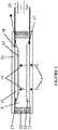
- the active pixel array component includes a vacuum enclosure 3 that houses a photocathode 12 in proximity focus with a specialized active pixel array sensor chip 13.
- the sensor chip 13 forms the anode for receiving proximity focused photoelectrons from the photocathode 12.
- the active pixel array sensor 13 is mounted with its backside facing the photocathode 12.
- the backside of the substrate of the active pixel array sensor 13 is thinned. Thinning the backside of the substrate provides for a greater collection efficiency of the photoelectron excited carriers and reduces the crosstalk between pixels as a result of diffusion.
- the active pixel sensor array 13 may also include a passivated surface or layer.
- a collimator assembly 10 is mounted on the backside of the pixel array sensor chip 13.
- the collimator assembly 10 spatially filters scattered electrons from the sensor chip 13 thereby minimizing image artifacts and improving the modulation transfer function (MTF) of the photocathode based electron bombarded active pixel sensor.
- MTF modulation transfer function
- the base of the vacuum device 3 is a transparent faceplate 21.
- the photocathode 12 is positioned on the faceplate 21.
- Vacuum enclosure sidewalls 22 extend between the transparent faceplate 21 and the header assembly 23.
- the active pixel sensor chip 13 is positioned on the header assembly 23.
- the header assembly 23 also allows for electrical feedthroughs for applying and reading back control voltages 17, bias voltage 18 and signal output lines 20 associated with the active pixel array sensor chip 13. Control electronics (not shown) are used to read out and operate the pixel array.
- the photocathode 12 can be a GaAs, an InP/InGaAs, a transferred electron photocathode, a multi-alkali photocathode, or any other photocathode known to those skilled in the art.
- An electron accelerating voltage 37 is applied to the photocathode 12.
- Photoelectrons 15 are emitted from the photocathode 12 in response to incident light in the form of an optical image 9.
- Optical components (not shown) are typically employed to form the optical image on the photocathode 12.
- a projection system may be used to place the image on the photocathode 12.
- An anode voltage 18 is applied to the sensor 13.
- the photoelectrons 15 are accelerated by virtue of the difference between the accelerating voltage 37 and the anode voltage 18.
- the accelerating voltage 37 is negative with respect to the anode voltage 18. This permits biasing the sensor 13 to near (or at) ground potential to simplify interfacing with other components.
- Control signals and bias voltages 17 are applied to the active pixel sensor 3 and a video output signal 20 may be taken off the sensor 13.
- the electron bombarded active pixel array sensor 13 is usefully employed in various systems, such as cameras, night vision imagers and the like.
- optical lenses or the like form an image of real objects on a focal plane which is ordinarily disposed to coincide with the photocathode 12.
- the focal plane is formed on the backside thinned surface of the pixel array and the bias may be adjusted to preclude the photoelectron flux 15 and operate in a conventional optical image regime.
- the electron bombarded active pixel array component with optics, power supply and control electronics may be regarded as a camera system.
- the image sensor 13 includes an array of nominally 10 micron square pixels with center to center displacement of approximately 10 microns and a 50 micron (height) collimator 10. It will be appreciated that the dimensions of the image sensor 13 and the collimator 10 may be less than or greater than these exemplary dimensions.
- FIG. 2 illustrates the operation of backside thinned sensor 13 and the collimator assembly 10 in further detail.
- an elemental collimator 40 i.e., an element of the collimator assembly 10
- the four pixel sub-array 42 is disposed within and proximate the front side of the sensor chip 13.
- the collimator is aligned with the pixel array when the normal to the center of a pixel (or center of a group of pixels) is collinear with the long axis of the corresponding collimator.
- An exemplary backscattered electron trajectory 46 is shown terminating on the interior walls 43 of the elemental collimator 40. But for the collimator 10, such backscattered electrons would excite pixels other than that pixel directly on the initial trajectory 44 of a proximity focused electron, thus degrading resolution and contributing artifact such as the halo effect. Thus, the collimator 10 functions as a baffle in respect to scattered electrons.
- the backscattered electrons are a relatively small effect and the halo effect, as such, becomes significant for very bright image features; however, the suppression of backscattered electrons is desirable because it is a source of background noise and veiling glare in the image sensor, resulting in reduced MTF.
- CMOS imagers typically show signs of damage if peak processing temperatures exceed about 450°C. This 450°C temperature limit makes the use of many active braze materials difficult. Thermo-compression bonds, brazes and solders typically do not bond well directly to a silicon surface. Accordingly, in embodiments of the present invention, a catch pad is provided on the solid state semiconductor imager to form a high reliability bond between the imager 13 and the collimator 10.
- FIG 3 is a detailed view of the exposed backside thinned, passivated semiconductor image array surface 45 illustrating an embodiment in which catch pads are used to form the high reliability bond.
- the catch pads 104 are deposited onto the backside, passivated surface 44 of the semiconductor image array.
- the catch pads 104 shown by dotted circles, are provided inside and outside of the pixel array region 42.
- the catch pads 104 are interspersed across the array surface 45.
- one catch pad is used for every four pixels. Consequently, a one megapixel imaging sensor employs on the order of 250,000 catch pads.
- the catch pads illustrated in Figure 3 cover about 0.2% of the focal plane area. It will be appreciated that these numbers are exemplary and that the imaging sensor may include less than or more than 250,000 catch pads, and the catch pads may cover less than or more than 0.2% of the focal plane area. In one embodiment, the catch pads do not exceed about 50% pixel coverage for a single pixel.
- Exemplary dimensions for the features of the image array surface are 10 micron pixel pitch, 40 micron collimator pitch, 1 micron collimator wall thickness and 4 micron diameter catch pads. It will be appreciated that these dimensions are only exemplary and that the dimensions may be less than or greater than the exemplary dimensions.
- the catch pad dimensions may be limited by the limitations of the existing lithography techniques. For example, currently available lithography techniques limit dimensions of the catch pads to about 0.1 microns. It will be appreciated that tradeoffs can be made between catch pad geometry and number.
- the catch pads can take the form of a line segment that exceeds the collimator pitch so that there is a collimator wall intersection even if the collimator is not aligned to the underlying pixel area.
- an alternate catch pad geometry is a 1 micron by 28.3 micron line segment aligned at a 45 degree angle to the pixel array.
- the catch pads 104 may be deposited using known deposition techniques, such as, for example, atomic layer deposition (ALD), electro-plating, chemical vapor deposition (CVD) and physical vapor deposition (PVD) processes, and the like, and combinations thereof.
- ALD atomic layer deposition
- CVD chemical vapor deposition
- PVD physical vapor deposition
- the collimator assembly 10 which includes a metallized surface, is then aligned and pressed into the catch pads 104. Thermal and pressure profiles are generated to generate a reliable metal bond between the collimator 10 and the image sensor 13.
- the pressure and temperature profile required to generate a reliable bond depends on the details of the metallization approach.
- gold to gold thermo-compression bond(s) may be used to join the collimator assembly 10 and the image sensor 3. In the case of gold to gold thermo-compression bonds, a temperature profile of 300°C for 10 minutes at a pressure sufficient to yield approximately a 30% compression of the overall gold thickness resulted in reliable bonds.
- FIG. 4 illustrates the catch pad layer structure in further detail.
- the catch pad 104 includes a top layer 105, an adhesion layer 107 and a barrier layer 109.
- the adhesion layer 107 is positioned between the top layer 105 and the barrier layer 109.
- the top layer 105 is used to form the metal bond with the metallized layer of the collimator 10.
- the catch pad assembly 104 shown in Figure 4 may be used with, for example, gold to gold thermo-compression bonding.
- the top layer 105 is gold.
- other metals may be used as the top layer.
- copper or silver can be cleaned to yield a reliable bond.
- the malleable, relatively non-reactive nature of gold provides certain advantages over other metals.
- Exemplary dimensions of the top layer 105 are 2 microns in diameter and 2 microns thickness. It will be appreciated that the metal thickness, however, may be any thickness between about 0.2 to more than 5 microns. In one particular embodiment, the thickness is two microns, which is sufficient to overcome surface irregularities without imposing excessive difficulty for the use of lift-off lithography.
- the adhesion layer 107 is provided to improve adhesion between the top layer 105 and the barrier layer 109.
- the adhesion layer 107 is titanium. It will be appreciated that the adhesion layer 107 may be other reactive metal materials. Other exemplary materials include but are not limited to Chromium, Tungsten, Niobium, Vanadium, and the like, and alloys thereof (e.g., Ti - W).
- the adhesion layer 107 is about 500 Angstroms thick. It will be appreciated that the thickness of the adhesion layer 107 may be less than or greater than 500 Angstroms.
- the barrier layer 109 is provided to prevent the overlying metal layers 105, 107 from reacting with or excessively stressing the underlying passivated, backside thinned semiconductor image array 13.
- the barrier layer 109 protects the sensor surface throughout the thermal and pressure cycles required for bonding and any subsequent UHV processing.
- the barrier layer 109 is approximately 1000 Angstroms and is made of SiO 2 .
- Other exemplary materials that may be used for the barrier layer 109 include but are not limited to SiO, SiO x N y , Al 2 O 3 ,and the like, and refractory metals, such as Tungsten, Molybdenum, Tantalum, Niobium, Platinum, and the like. It will be appreciated that the thickness of the barrier layer 109 may be less than or greater than 1000 Angstroms.
- barrier layer 109 typically, there is sufficient leakage to drain off the photocathode charge without the need for a discrete "grounding" contact; however, if the nature and thickness of the barrier layer 109 results in an electrically isolated bond, a path is provided to assure that the collimator remains at the potential of the underlying anode.
- One such path eliminates the barrier layer 109 for bonds that lie outside of the imaging area (but the barrier layer 109 remains for those bonds that lie within the imaging area).
- the adhesion layer 107 and barrier layer 109 may be combined (i.e., a single layer may be deposited under the top layer 105).
- top layer 105, adhesion layer 107 and barrier 109 may be deposited using known techniques such as for example atomic layer deposition (ALD), electro-plating, chemical vapor deposition (CVD) and physical vapor deposition (PVD) processes, and the like, and combinations thereof.
- ALD atomic layer deposition
- CVD chemical vapor deposition
- PVD physical vapor deposition
- Figure 5 illustrates the metal bond between the collimator 40 and the image sensor 13 in further detail.
- Two metal layers are deposited on the silicon walls of the collimator 40 so the collimator 40 can be joined with the catch pads 104.
- the two metal layers include an adhesion layer 62 and a surface layer 65.
- the adhesion layer 62 improves adhesion between the surface layer 65 and the silicon collimator 40.
- the adhesion layer 62 is Titanium and 500 Angstroms in thickness. It will be appreciated that the adhesion layer 62 may be made of any reactive metal. Other suitable materials include but are not limited to Chromium, Tungsten, Niobium, Vanadium, and the like, and alloys thereof (e.g., Ti - W). It will be appreciated that the thickness of the adhesion layer 62 may be less than or greater than 500 Angstroms.
- the bottom layer 65 is gold.
- Exemplary dimensions of the bottom layer 65 are 1 micron wide (e.g., the width of a collimator wall) and 2 microns thick. It will be appreciated that these dimensions are merely exemplary and that the dimensions may be less than or greater than these exemplary dimensions.
- the full surface of the collimator 40 may be coated by the surface layer 65.
- a residual separation is shown between the top of the free surface of the collimator (defined by layer 65) and the free surface of the imager 13.
- the separation between the two surfaces is approximately 1 micron. This separation is sufficient to insure that residual movement of the collimator under gated proximity focused sensor operation does not result in imager damage.
- geometry and pressure are primary factors in controlling the residual collimator-to-sensor gap in the regions between catch pads.
- thermo-compression bond is used to form the metal bond between the image sensor 13 and the collimator 10.
- a temperature of 300°C for 10 minutes at a sufficient pressure can yield about a 10% to about a 50% compression of the overall gold thickness, which results in reliable bonds.
- the collimator 10 and image sensor 13 may be bonded using other bonding techniques such as, for example, brazing and soldering.
- the layers 107 and 109 may be thickened to insure that a minimal residual collimator-to-sensor gap is maintained in the regions between the catch pads 104.
- the top layer 105 may instead be a braze alloy such as for example Au - Sn.
- the time and temperature of the bond may be set to allow inter-diffusion between the top layer 105 of the imaging sensor 13 and the bottom layer 65 of the collimator 40 to increase the melting point of the bond beyond that of the eutectic value.
- Braze metallizations that terminate in gold (Au) are advantageous because surface oxidation issues are avoided thereby improving braze reliability.
- Those skilled in the art of brazing can apply a wide variety of material systems to this bond while maintaining the disclosed geometry and meeting the constraints imposed by UHV processing.
- the small catch pad geometry ( ⁇ 5 microns wide) is important when high modulus higher melting point braze alloys are used.
- Other suitable solder / braze alloys include but are not limited to Gold - Silicon, Gold - Germanium and Gold - Tin. Transient liquid phase (TLP) braze-formulations / thermal profiles may also be used.
- a collimator structure that is hexagonal, and has a 17 micron pitch, 50 micron thick with a wall thickness of ⁇ 1 micron can be used in conjunction with 20 micron long, 2 micron wide catch pads, and the image sensor can be a backside thinned electron bombarded active pixel sensor with a 10.8 micron pixel pitch.
- Image testing of EBAPS sensors incorporating collimators bonded via metal bonds on catch pads showed the electron shadow of the collimator and catch pad are very stable over the life of the sensor.
- Catch pads and collimator wall thickness were designed such that individual pixel shadowing ranged from 0 to ⁇ 40%. Limiting pixel shadowing to this range combined with the stable nature of the shadowing allows image correction algorithms to reliably correct for any reduced gain on the affected pixels.
- aligning collimator geometry to pixel geometry still results in the best possible image sensor performance, the stability of the fixed pattern noise combined with image correction algorithms allows non-aligned catch pad and collimator geometries to be used with minimal performance degradation, which, in turn, lowers the capital equipment cost required to produce the bonded collimator anode assemblies.
- the bonding techniques disclosed herein can be used with front-surface electron sensitive read out integrated circuits (ROICs).
- the underlying barrier layer may be omitted; the metal pads can rest directly on the SiOxNy barrier layer found in these sensors.
- the catch pads on the front-side imagers can be built up from metal pads, providing direct electrical connection to the collimator.
Landscapes
- Engineering & Computer Science (AREA)
- Mechanical Engineering (AREA)
- Chemical & Material Sciences (AREA)
- Materials Engineering (AREA)
- Multimedia (AREA)
- Signal Processing (AREA)
- Solid State Image Pick-Up Elements (AREA)
- Transforming Light Signals Into Electric Signals (AREA)
- Image-Pickup Tubes, Image-Amplification Tubes, And Storage Tubes (AREA)
Claims (14)
- Bildsensor, umfassend:einen Festkörper-Halbleiter-Bildaufnehmer mit einer Sensoranode und einem Pixelarray-Bereich; undeinen Kollimator (10) mit einer metallisierten Schicht, die der Sensoranode zugewandt ist,dadurch gekennzeichnet,dass eine Vielzahl metallisierter Fangpads (104) innerhalb des Pixelarray-Bereichs verteilt angeordnet ist, unddass die metallisierte Schicht mit den metallisierten Fangpads (104) zu einer Metallverbindung verbunden wird.
- Bildsensor nach Anspruch 1, dadurch gekennzeichnet, dass der Festkörper-Halbleiter-Bildaufnehmer einen rückseitig verdünnten Pixelarraysensor (13) umfasst und eine passivierte Siliziumoberfläche (44) aufweist, wobei ein Teil der passivierten Siliziumoberfläche einen Pixelarray-Bereich (45) beinhaltet; und
die Metallverbindung innerhalb des Pixelarray-Bereichs (45) die passivierte Siliziumoberfläche (44) des Festkörper-Halbleiter-Bildaufnehmers mit dem Siliziumkollimator (10) verbindet. - Bildsensor nach Anspruch 2, bei dem die Fangpads (104) thermokomprimierte metallisierte Fangpads (104) oder hartgelötete metallisierte Fangpads (104) umfasst und die Metallverbindung des Weiteren Metallschichten umfasst, die auf den Siliziumwänden des Kollimators (10) aufgebracht sind.
- Bildsensor nach Anspruch 2 oder 3, bei dem jedes der Fangpads (104) eine oberste Metallschicht (105), eine Haftschicht (107) und eine Sperrschicht (109) auf der passivierten Siliziumoberfläche (44) umfasst.
- Bildsensor nach Anspruch 1 oder 2, bei dem jedes der metallisierten Fangpads (104) eine oberste Metallschicht (105) und eine Sperrschicht (109) sowie fakultativ eine Haftschicht (107) umfasst.
- Bildsensor nach einem der vorhergehenden Ansprüche, bei dem jedes der metallisierten Fangpads (104) eine Goldschicht, eine Titanschicht und eine SiOxNy-Schicht umfasst.
- Bildsensor nach Anspruch 1, bei dem der Kollimator (10) des Weiteren eine Haftschicht zwischen einem Kollimatorkörper des Kollimators (10) und der metallisierten Schicht umfasst.
- Bildsensor nach einem der vorhergehenden Ansprüche, bei dem sich die Vielzahl der metallisierten Fangpads (104) innerhalb und außerhalb des Pixelarray-Bereichs (45) befindet.
- Bildsensor nach einem der vorhergehenden Ansprüche, bei dem der Festkörper-Halbleiter-Bildaufnehmer ein rückseitig verdünnter Pixelarraysensor mit passivierter Oberfläche ist.
- Bildsensor nach Anspruch 1, bei den die Metallverbindung durch ein Thermokompressionsverfahren oder durch ein Hartlötverfahren gebildet wird.
- Verfahren zur Herstellung eines Bildsensors, der einen Festkörper-Halbleiter-Bildaufnehmer mit einer Sensoranode und einem Pixelarray-Bereich (45) umfasst, bei dem eine Metallschicht, die der Sensoranode zugewandt ist, auf einem Kollimator (10) aufgebracht wird,
gekennzeichnet durch
das Aufbringen einer Vielzahl von Fangpads (104) auf einer rückseitigen passivierten Oberfläche (44) eines Halbleiter-Bildarrays derart, dass sie in dem gesamten Bilderfassungsarray eines Festkörper-Halbleiter-Bildaufnehmers verteilt sind;
einen Kollimator (10);
das Ausrichten des Kollimators (10) mit dem Festkörper-Halbleiter-Bildaufnehmer; und
das Verbinden des Kollimators (10) mit dem Festkörper-Halbleiter-Bildaufnehmer zur Bildung einer Metallverbindung zwischen dem Kollimator (10) und dem Festkörper-Halbleiter-Bildaufnehmer, wobei sich die Metallverbindung in einem Pixelarray-Bereich (45) des Festkörper-Halbleiter-Bildaufnehmers befindet. - Verfahren nach Anspruch 11, bei dem das Verbinden des Kollimators (10) mit dem Festkörper-Halbteiter-Bildaufnehmer zur Bildung der Metallverbindung das Durchführen eines Thermokompressionsverfahrens oder eines Hartlötverfahrens oder eines Weichlötverfahrens umfasst.
- Verfahren nach Anspruch 11, bei dem das Aufbringen einer Vielzahl von Fangpads (104) folgendes umfasst:
Aufbringen einer Sperrschicht (109) auf dem Festkörper-Bildsensor, und Aufbringen einer obersten Metallschicht (105) auf der Haftschicht (107), und fakultativ Aufbringen einer Haftschicht (107) auf der Sperrschicht (109). - Verfahren nach Anspruch 11, bei dem der Festkörper-Halbleiter-Bildaufnehmer ein metallisches Fangpad umfasst und der Kollimator (10) eine metallisierte Schicht umfasst, und bei dem das Verbinden des Kollimators (10) mit dem Festkörper-Halbleiter-Bildaufnehmer zur Bildung der Metallverbindung das Verbinden der metallischen Fangpads (104) mit der metallisierten Schicht umfasst.
Applications Claiming Priority (2)
| Application Number | Priority Date | Filing Date | Title |
|---|---|---|---|
| US12/764,862 US8698925B2 (en) | 2010-04-21 | 2010-04-21 | Collimator bonding structure and method |
| PCT/US2011/033496 WO2012021182A1 (en) | 2010-04-21 | 2011-04-21 | Collimator bonding structure and method |
Publications (3)
| Publication Number | Publication Date |
|---|---|
| EP2561675A1 EP2561675A1 (de) | 2013-02-27 |
| EP2561675A4 EP2561675A4 (de) | 2017-08-09 |
| EP2561675B1 true EP2561675B1 (de) | 2018-09-19 |
Family
ID=44815512
Family Applications (1)
| Application Number | Title | Priority Date | Filing Date |
|---|---|---|---|
| EP11816721.2A Not-in-force EP2561675B1 (de) | 2010-04-21 | 2011-04-21 | Bildsensor und verfahren zur herstellung eines bildsensors |
Country Status (9)
| Country | Link |
|---|---|
| US (1) | US8698925B2 (de) |
| EP (1) | EP2561675B1 (de) |
| JP (1) | JP5798181B2 (de) |
| KR (2) | KR101783594B1 (de) |
| AU (1) | AU2011289856B2 (de) |
| BR (1) | BR112012027026A2 (de) |
| CA (1) | CA2797134C (de) |
| IL (1) | IL222569A (de) |
| WO (1) | WO2012021182A1 (de) |
Families Citing this family (9)
| Publication number | Priority date | Publication date | Assignee | Title |
|---|---|---|---|---|
| US8698925B2 (en) | 2010-04-21 | 2014-04-15 | Intevac, Inc. | Collimator bonding structure and method |
| JP5065516B2 (ja) * | 2010-08-04 | 2012-11-07 | エフ イー アイ カンパニ | 薄い電子検出器における後方散乱の減少 |
| RU2523193C2 (ru) * | 2012-04-19 | 2014-07-20 | Федеральное государственное бюджетное образовательное учреждение высшего профессионального образования "Тольяттинский государственный университет" | Контейнер для пайки |
| US9177764B1 (en) | 2013-11-11 | 2015-11-03 | Exelis, Inc. | Image intensifier having an ion barrier with conductive material and method for making the same |
| US9734977B2 (en) | 2015-07-16 | 2017-08-15 | Intevac, Inc. | Image intensifier with indexed compliant anode assembly |
| CN107980219B (zh) * | 2017-10-20 | 2021-08-20 | 深圳市汇顶科技股份有限公司 | 像素传感模块及图像撷取装置 |
| US10163599B1 (en) | 2018-01-03 | 2018-12-25 | Eagle Technology, Llc | Electron multiplier for MEMs light detection device |
| US11621289B2 (en) * | 2020-05-22 | 2023-04-04 | Eotech, Llc | Compact proximity focused image sensor |
| JP7624822B2 (ja) * | 2020-11-04 | 2025-01-31 | Gpixel Japan株式会社 | 裏面照射型cmosセンサの製造方法、電子衝撃型cmosセンサの製造方法、裏面照射型cmosセンサ用画素、および電子衝撃型cmosセンサ |
Family Cites Families (22)
| Publication number | Priority date | Publication date | Assignee | Title |
|---|---|---|---|---|
| US550193A (en) | 1895-11-19 | Sack or barrel transfer | ||
| FR2574239B1 (fr) | 1984-11-30 | 1987-01-23 | Labo Electronique Physique | Capteur d'images pour camera fonctionnant en mode " jour-nuit " |
| US5688715A (en) | 1990-03-29 | 1997-11-18 | The United States Of America As Represented By The Secretary Of The Navy | Excimer laser dopant activation of backside illuminated CCD's |
| US5404047A (en) * | 1992-07-17 | 1995-04-04 | Lsi Logic Corporation | Semiconductor die having a high density array of composite bond pads |
| DE4241045C1 (de) | 1992-12-05 | 1994-05-26 | Bosch Gmbh Robert | Verfahren zum anisotropen Ätzen von Silicium |
| US5495141A (en) | 1994-02-15 | 1996-02-27 | The Regents Of The University Of California | Collimator application for microchannel plate image intensifier resolution improvement |
| US6094114A (en) * | 1994-09-26 | 2000-07-25 | Endgate Corporation | Slotline-to-slotline mounted flip chip |
| US5661081A (en) * | 1994-09-30 | 1997-08-26 | United Microelectronics Corporation | Method of bonding an aluminum wire to an intergrated circuit bond pad |
| JP3054056B2 (ja) | 1995-04-24 | 2000-06-19 | 株式会社日立製作所 | はんだ付け方法 |
| US6483231B1 (en) | 1999-05-07 | 2002-11-19 | Litton Systems, Inc. | Night vision device and method |
| US6285018B1 (en) | 1999-07-20 | 2001-09-04 | Intevac, Inc. | Electron bombarded active pixel sensor |
| US7042060B2 (en) | 2003-01-31 | 2006-05-09 | Intevac, Inc. | Backside thinning of image array devices |
| US7005637B2 (en) * | 2003-01-31 | 2006-02-28 | Intevac, Inc. | Backside thinning of image array devices |
| US20040169248A1 (en) * | 2003-01-31 | 2004-09-02 | Intevac, Inc. | Backside thinning of image array devices |
| US7214999B2 (en) * | 2003-10-31 | 2007-05-08 | Motorola, Inc. | Integrated photoserver for CMOS imagers |
| US9470801B2 (en) * | 2004-01-13 | 2016-10-18 | Spectrum Dynamics Llc | Gating with anatomically varying durations |
| TWI237860B (en) * | 2004-02-13 | 2005-08-11 | Advanced Semiconductor Eng | Integrated chip structure for wire bonding and flip chip assembly package and fabrication process thereof |
| JP3994980B2 (ja) * | 2004-03-29 | 2007-10-24 | 株式会社日立製作所 | 素子搭載用基板及びその製造方法並びに半導体素子実装方法 |
| US7607560B2 (en) * | 2004-05-14 | 2009-10-27 | Intevac, Inc. | Semiconductor die attachment for high vacuum tubes |
| US8836146B2 (en) * | 2006-03-02 | 2014-09-16 | Qualcomm Incorporated | Chip package and method for fabricating the same |
| TW200910580A (en) | 2007-08-17 | 2009-03-01 | Hsin-Hui Yeh | CMOS image sensor package and method thereof |
| US8698925B2 (en) | 2010-04-21 | 2014-04-15 | Intevac, Inc. | Collimator bonding structure and method |
-
2010
- 2010-04-21 US US12/764,862 patent/US8698925B2/en active Active
-
2011
- 2011-04-21 KR KR1020177017283A patent/KR101783594B1/ko active Active
- 2011-04-21 JP JP2013506312A patent/JP5798181B2/ja active Active
- 2011-04-21 AU AU2011289856A patent/AU2011289856B2/en not_active Ceased
- 2011-04-21 CA CA2797134A patent/CA2797134C/en active Active
- 2011-04-21 WO PCT/US2011/033496 patent/WO2012021182A1/en not_active Ceased
- 2011-04-21 BR BR112012027026A patent/BR112012027026A2/pt not_active IP Right Cessation
- 2011-04-21 KR KR1020127030372A patent/KR101752150B1/ko not_active Expired - Fee Related
- 2011-04-21 EP EP11816721.2A patent/EP2561675B1/de not_active Not-in-force
-
2012
- 2012-10-21 IL IL222569A patent/IL222569A/en active IP Right Grant
Non-Patent Citations (1)
| Title |
|---|
| None * |
Also Published As
| Publication number | Publication date |
|---|---|
| WO2012021182A1 (en) | 2012-02-16 |
| BR112012027026A2 (pt) | 2016-07-19 |
| IL222569A0 (en) | 2012-12-31 |
| EP2561675A1 (de) | 2013-02-27 |
| KR20170075817A (ko) | 2017-07-03 |
| US20110261239A1 (en) | 2011-10-27 |
| EP2561675A4 (de) | 2017-08-09 |
| CA2797134A1 (en) | 2012-02-16 |
| AU2011289856A9 (en) | 2014-01-30 |
| KR20130051948A (ko) | 2013-05-21 |
| IL222569A (en) | 2017-09-28 |
| AU2011289856A1 (en) | 2012-11-22 |
| CA2797134C (en) | 2019-02-19 |
| US8698925B2 (en) | 2014-04-15 |
| WO2012021182A4 (en) | 2012-05-03 |
| KR101752150B1 (ko) | 2017-06-29 |
| JP2013529356A (ja) | 2013-07-18 |
| AU2011289856A2 (en) | 2013-03-07 |
| AU2011289856B2 (en) | 2015-02-12 |
| KR101783594B1 (ko) | 2017-10-10 |
| JP5798181B2 (ja) | 2015-10-21 |
Similar Documents
| Publication | Publication Date | Title |
|---|---|---|
| EP2561675B1 (de) | Bildsensor und verfahren zur herstellung eines bildsensors | |
| US7005637B2 (en) | Backside thinning of image array devices | |
| US7199345B1 (en) | Low profile wire bond for an electron sensing device in an image intensifier tube | |
| WO2005114727A2 (en) | Semiconductor die attachment for high vaccum tubes | |
| US7042060B2 (en) | Backside thinning of image array devices | |
| US12002834B2 (en) | Compact proximity focused image sensor | |
| JP2010103117A (ja) | 画像増強装置 | |
| EP1038317B1 (de) | Substratanordnung für eine integrierte schaltung und herstellungsverfahren dafür | |
| JP2008547189A (ja) | 電子打ち込み型イメージセンサアレイ装置及びそのイメージセンサアレイ | |
| EP1741143A1 (de) | Rückseitenverdünnung von bild-array-einrichtungen | |
| McPhate et al. | Noiseless, kilohertz-frame-rate, imaging detector based on microchannel plates readout with the medipix2 cmos pixel chip | |
| CA2612058C (en) | Electron bombarded image sensor array device and its manufactoring method |
Legal Events
| Date | Code | Title | Description |
|---|---|---|---|
| PUAI | Public reference made under article 153(3) epc to a published international application that has entered the european phase |
Free format text: ORIGINAL CODE: 0009012 |
|
| 17P | Request for examination filed |
Effective date: 20121109 |
|
| AK | Designated contracting states |
Kind code of ref document: A1 Designated state(s): AL AT BE BG CH CY CZ DE DK EE ES FI FR GB GR HR HU IE IS IT LI LT LU LV MC MK MT NL NO PL PT RO RS SE SI SK SM TR |
|
| DAX | Request for extension of the european patent (deleted) | ||
| RA4 | Supplementary search report drawn up and despatched (corrected) |
Effective date: 20170711 |
|
| RIC1 | Information provided on ipc code assigned before grant |
Ipc: B23K 101/42 20060101ALN20170706BHEP Ipc: B23K 1/19 20060101ALI20170706BHEP Ipc: B23K 103/00 20060101ALN20170706BHEP Ipc: B23K 1/00 20060101AFI20170706BHEP Ipc: H01L 27/146 20060101ALI20170706BHEP Ipc: B23K 1/20 20060101ALI20170706BHEP |
|
| RIC1 | Information provided on ipc code assigned before grant |
Ipc: B23K 1/20 20060101ALI20180112BHEP Ipc: B23K 1/19 20060101ALI20180112BHEP Ipc: B23K 1/00 20060101AFI20180112BHEP Ipc: H01L 27/146 20060101ALI20180112BHEP Ipc: B23K 103/00 20060101ALN20180112BHEP Ipc: B23K 101/42 20060101ALN20180112BHEP |
|
| GRAP | Despatch of communication of intention to grant a patent |
Free format text: ORIGINAL CODE: EPIDOSNIGR1 |
|
| STAA | Information on the status of an ep patent application or granted ep patent |
Free format text: STATUS: GRANT OF PATENT IS INTENDED |
|
| INTG | Intention to grant announced |
Effective date: 20180305 |
|
| GRAJ | Information related to disapproval of communication of intention to grant by the applicant or resumption of examination proceedings by the epo deleted |
Free format text: ORIGINAL CODE: EPIDOSDIGR1 |
|
| STAA | Information on the status of an ep patent application or granted ep patent |
Free format text: STATUS: REQUEST FOR EXAMINATION WAS MADE |
|
| REG | Reference to a national code |
Ref country code: DE Ref legal event code: R079 Ref document number: 602011052245 Country of ref document: DE Free format text: PREVIOUS MAIN CLASS: H04N0005335000 Ipc: B23K0001000000 |
|
| GRAS | Grant fee paid |
Free format text: ORIGINAL CODE: EPIDOSNIGR3 |
|
| STAA | Information on the status of an ep patent application or granted ep patent |
Free format text: STATUS: GRANT OF PATENT IS INTENDED |
|
| GRAP | Despatch of communication of intention to grant a patent |
Free format text: ORIGINAL CODE: EPIDOSNIGR1 |
|
| INTC | Intention to grant announced (deleted) | ||
| RIC1 | Information provided on ipc code assigned before grant |
Ipc: B23K 103/00 20060101ALN20180626BHEP Ipc: B23K 101/42 20060101ALN20180626BHEP Ipc: B23K 1/19 20060101ALI20180626BHEP Ipc: B23K 1/00 20060101AFI20180626BHEP Ipc: H01L 27/146 20060101ALI20180626BHEP Ipc: B23K 1/20 20060101ALI20180626BHEP |
|
| GRAA | (expected) grant |
Free format text: ORIGINAL CODE: 0009210 |
|
| STAA | Information on the status of an ep patent application or granted ep patent |
Free format text: STATUS: THE PATENT HAS BEEN GRANTED |
|
| INTG | Intention to grant announced |
Effective date: 20180726 |
|
| AK | Designated contracting states |
Kind code of ref document: B1 Designated state(s): AL AT BE BG CH CY CZ DE DK EE ES FI FR GB GR HR HU IE IS IT LI LT LU LV MC MK MT NL NO PL PT RO RS SE SI SK SM TR |
|
| REG | Reference to a national code |
Ref country code: GB Ref legal event code: FG4D |
|
| REG | Reference to a national code |
Ref country code: CH Ref legal event code: EP |
|
| REG | Reference to a national code |
Ref country code: AT Ref legal event code: REF Ref document number: 1042670 Country of ref document: AT Kind code of ref document: T Effective date: 20181015 |
|
| REG | Reference to a national code |
Ref country code: IE Ref legal event code: FG4D |
|
| REG | Reference to a national code |
Ref country code: DE Ref legal event code: R096 Ref document number: 602011052245 Country of ref document: DE |
|
| REG | Reference to a national code |
Ref country code: NL Ref legal event code: FP |
|
| PG25 | Lapsed in a contracting state [announced via postgrant information from national office to epo] |
Ref country code: LT Free format text: LAPSE BECAUSE OF FAILURE TO SUBMIT A TRANSLATION OF THE DESCRIPTION OR TO PAY THE FEE WITHIN THE PRESCRIBED TIME-LIMIT Effective date: 20180919 Ref country code: RS Free format text: LAPSE BECAUSE OF FAILURE TO SUBMIT A TRANSLATION OF THE DESCRIPTION OR TO PAY THE FEE WITHIN THE PRESCRIBED TIME-LIMIT Effective date: 20180919 Ref country code: NO Free format text: LAPSE BECAUSE OF FAILURE TO SUBMIT A TRANSLATION OF THE DESCRIPTION OR TO PAY THE FEE WITHIN THE PRESCRIBED TIME-LIMIT Effective date: 20181219 Ref country code: SE Free format text: LAPSE BECAUSE OF FAILURE TO SUBMIT A TRANSLATION OF THE DESCRIPTION OR TO PAY THE FEE WITHIN THE PRESCRIBED TIME-LIMIT Effective date: 20180919 Ref country code: FI Free format text: LAPSE BECAUSE OF FAILURE TO SUBMIT A TRANSLATION OF THE DESCRIPTION OR TO PAY THE FEE WITHIN THE PRESCRIBED TIME-LIMIT Effective date: 20180919 Ref country code: GR Free format text: LAPSE BECAUSE OF FAILURE TO SUBMIT A TRANSLATION OF THE DESCRIPTION OR TO PAY THE FEE WITHIN THE PRESCRIBED TIME-LIMIT Effective date: 20181220 Ref country code: BG Free format text: LAPSE BECAUSE OF FAILURE TO SUBMIT A TRANSLATION OF THE DESCRIPTION OR TO PAY THE FEE WITHIN THE PRESCRIBED TIME-LIMIT Effective date: 20181219 |
|
| REG | Reference to a national code |
Ref country code: LT Ref legal event code: MG4D |
|
| PG25 | Lapsed in a contracting state [announced via postgrant information from national office to epo] |
Ref country code: HR Free format text: LAPSE BECAUSE OF FAILURE TO SUBMIT A TRANSLATION OF THE DESCRIPTION OR TO PAY THE FEE WITHIN THE PRESCRIBED TIME-LIMIT Effective date: 20180919 Ref country code: LV Free format text: LAPSE BECAUSE OF FAILURE TO SUBMIT A TRANSLATION OF THE DESCRIPTION OR TO PAY THE FEE WITHIN THE PRESCRIBED TIME-LIMIT Effective date: 20180919 Ref country code: AL Free format text: LAPSE BECAUSE OF FAILURE TO SUBMIT A TRANSLATION OF THE DESCRIPTION OR TO PAY THE FEE WITHIN THE PRESCRIBED TIME-LIMIT Effective date: 20180919 |
|
| REG | Reference to a national code |
Ref country code: AT Ref legal event code: MK05 Ref document number: 1042670 Country of ref document: AT Kind code of ref document: T Effective date: 20180919 |
|
| PG25 | Lapsed in a contracting state [announced via postgrant information from national office to epo] |
Ref country code: CZ Free format text: LAPSE BECAUSE OF FAILURE TO SUBMIT A TRANSLATION OF THE DESCRIPTION OR TO PAY THE FEE WITHIN THE PRESCRIBED TIME-LIMIT Effective date: 20180919 Ref country code: IT Free format text: LAPSE BECAUSE OF FAILURE TO SUBMIT A TRANSLATION OF THE DESCRIPTION OR TO PAY THE FEE WITHIN THE PRESCRIBED TIME-LIMIT Effective date: 20180919 Ref country code: RO Free format text: LAPSE BECAUSE OF FAILURE TO SUBMIT A TRANSLATION OF THE DESCRIPTION OR TO PAY THE FEE WITHIN THE PRESCRIBED TIME-LIMIT Effective date: 20180919 Ref country code: ES Free format text: LAPSE BECAUSE OF FAILURE TO SUBMIT A TRANSLATION OF THE DESCRIPTION OR TO PAY THE FEE WITHIN THE PRESCRIBED TIME-LIMIT Effective date: 20180919 Ref country code: AT Free format text: LAPSE BECAUSE OF FAILURE TO SUBMIT A TRANSLATION OF THE DESCRIPTION OR TO PAY THE FEE WITHIN THE PRESCRIBED TIME-LIMIT Effective date: 20180919 Ref country code: EE Free format text: LAPSE BECAUSE OF FAILURE TO SUBMIT A TRANSLATION OF THE DESCRIPTION OR TO PAY THE FEE WITHIN THE PRESCRIBED TIME-LIMIT Effective date: 20180919 Ref country code: IS Free format text: LAPSE BECAUSE OF FAILURE TO SUBMIT A TRANSLATION OF THE DESCRIPTION OR TO PAY THE FEE WITHIN THE PRESCRIBED TIME-LIMIT Effective date: 20190119 Ref country code: PL Free format text: LAPSE BECAUSE OF FAILURE TO SUBMIT A TRANSLATION OF THE DESCRIPTION OR TO PAY THE FEE WITHIN THE PRESCRIBED TIME-LIMIT Effective date: 20180919 |
|
| PG25 | Lapsed in a contracting state [announced via postgrant information from national office to epo] |
Ref country code: SK Free format text: LAPSE BECAUSE OF FAILURE TO SUBMIT A TRANSLATION OF THE DESCRIPTION OR TO PAY THE FEE WITHIN THE PRESCRIBED TIME-LIMIT Effective date: 20180919 Ref country code: PT Free format text: LAPSE BECAUSE OF FAILURE TO SUBMIT A TRANSLATION OF THE DESCRIPTION OR TO PAY THE FEE WITHIN THE PRESCRIBED TIME-LIMIT Effective date: 20190119 Ref country code: SM Free format text: LAPSE BECAUSE OF FAILURE TO SUBMIT A TRANSLATION OF THE DESCRIPTION OR TO PAY THE FEE WITHIN THE PRESCRIBED TIME-LIMIT Effective date: 20180919 |
|
| REG | Reference to a national code |
Ref country code: DE Ref legal event code: R097 Ref document number: 602011052245 Country of ref document: DE |
|
| PLBE | No opposition filed within time limit |
Free format text: ORIGINAL CODE: 0009261 |
|
| STAA | Information on the status of an ep patent application or granted ep patent |
Free format text: STATUS: NO OPPOSITION FILED WITHIN TIME LIMIT |
|
| PG25 | Lapsed in a contracting state [announced via postgrant information from national office to epo] |
Ref country code: DK Free format text: LAPSE BECAUSE OF FAILURE TO SUBMIT A TRANSLATION OF THE DESCRIPTION OR TO PAY THE FEE WITHIN THE PRESCRIBED TIME-LIMIT Effective date: 20180919 |
|
| 26N | No opposition filed |
Effective date: 20190620 |
|
| PG25 | Lapsed in a contracting state [announced via postgrant information from national office to epo] |
Ref country code: SI Free format text: LAPSE BECAUSE OF FAILURE TO SUBMIT A TRANSLATION OF THE DESCRIPTION OR TO PAY THE FEE WITHIN THE PRESCRIBED TIME-LIMIT Effective date: 20180919 |
|
| REG | Reference to a national code |
Ref country code: CH Ref legal event code: PL |
|
| REG | Reference to a national code |
Ref country code: BE Ref legal event code: MM Effective date: 20190430 |
|
| PG25 | Lapsed in a contracting state [announced via postgrant information from national office to epo] |
Ref country code: MC Free format text: LAPSE BECAUSE OF FAILURE TO SUBMIT A TRANSLATION OF THE DESCRIPTION OR TO PAY THE FEE WITHIN THE PRESCRIBED TIME-LIMIT Effective date: 20180919 Ref country code: LU Free format text: LAPSE BECAUSE OF NON-PAYMENT OF DUE FEES Effective date: 20190421 |
|
| PG25 | Lapsed in a contracting state [announced via postgrant information from national office to epo] |
Ref country code: LI Free format text: LAPSE BECAUSE OF NON-PAYMENT OF DUE FEES Effective date: 20190430 Ref country code: CH Free format text: LAPSE BECAUSE OF NON-PAYMENT OF DUE FEES Effective date: 20190430 |
|
| PG25 | Lapsed in a contracting state [announced via postgrant information from national office to epo] |
Ref country code: BE Free format text: LAPSE BECAUSE OF NON-PAYMENT OF DUE FEES Effective date: 20190430 |
|
| PG25 | Lapsed in a contracting state [announced via postgrant information from national office to epo] |
Ref country code: TR Free format text: LAPSE BECAUSE OF FAILURE TO SUBMIT A TRANSLATION OF THE DESCRIPTION OR TO PAY THE FEE WITHIN THE PRESCRIBED TIME-LIMIT Effective date: 20180919 |
|
| PG25 | Lapsed in a contracting state [announced via postgrant information from national office to epo] |
Ref country code: IE Free format text: LAPSE BECAUSE OF NON-PAYMENT OF DUE FEES Effective date: 20190421 |
|
| PG25 | Lapsed in a contracting state [announced via postgrant information from national office to epo] |
Ref country code: CY Free format text: LAPSE BECAUSE OF FAILURE TO SUBMIT A TRANSLATION OF THE DESCRIPTION OR TO PAY THE FEE WITHIN THE PRESCRIBED TIME-LIMIT Effective date: 20180919 |
|
| PG25 | Lapsed in a contracting state [announced via postgrant information from national office to epo] |
Ref country code: HU Free format text: LAPSE BECAUSE OF FAILURE TO SUBMIT A TRANSLATION OF THE DESCRIPTION OR TO PAY THE FEE WITHIN THE PRESCRIBED TIME-LIMIT; INVALID AB INITIO Effective date: 20110421 Ref country code: MT Free format text: LAPSE BECAUSE OF FAILURE TO SUBMIT A TRANSLATION OF THE DESCRIPTION OR TO PAY THE FEE WITHIN THE PRESCRIBED TIME-LIMIT Effective date: 20180919 |
|
| PGFP | Annual fee paid to national office [announced via postgrant information from national office to epo] |
Ref country code: GB Payment date: 20220303 Year of fee payment: 12 |
|
| PGFP | Annual fee paid to national office [announced via postgrant information from national office to epo] |
Ref country code: NL Payment date: 20220314 Year of fee payment: 12 Ref country code: FR Payment date: 20220308 Year of fee payment: 12 |
|
| PG25 | Lapsed in a contracting state [announced via postgrant information from national office to epo] |
Ref country code: MK Free format text: LAPSE BECAUSE OF FAILURE TO SUBMIT A TRANSLATION OF THE DESCRIPTION OR TO PAY THE FEE WITHIN THE PRESCRIBED TIME-LIMIT Effective date: 20180919 |
|
| PGFP | Annual fee paid to national office [announced via postgrant information from national office to epo] |
Ref country code: DE Payment date: 20220302 Year of fee payment: 12 |
|
| P01 | Opt-out of the competence of the unified patent court (upc) registered |
Effective date: 20230802 |
|
| REG | Reference to a national code |
Ref country code: DE Ref legal event code: R119 Ref document number: 602011052245 Country of ref document: DE |
|
| REG | Reference to a national code |
Ref country code: NL Ref legal event code: MM Effective date: 20230501 |
|
| GBPC | Gb: european patent ceased through non-payment of renewal fee |
Effective date: 20230421 |
|
| PG25 | Lapsed in a contracting state [announced via postgrant information from national office to epo] |
Ref country code: GB Free format text: LAPSE BECAUSE OF NON-PAYMENT OF DUE FEES Effective date: 20230421 |
|
| PG25 | Lapsed in a contracting state [announced via postgrant information from national office to epo] |
Ref country code: NL Free format text: LAPSE BECAUSE OF NON-PAYMENT OF DUE FEES Effective date: 20230501 Ref country code: GB Free format text: LAPSE BECAUSE OF NON-PAYMENT OF DUE FEES Effective date: 20230421 Ref country code: FR Free format text: LAPSE BECAUSE OF NON-PAYMENT OF DUE FEES Effective date: 20230430 Ref country code: DE Free format text: LAPSE BECAUSE OF NON-PAYMENT OF DUE FEES Effective date: 20231103 |