EP2559984B1 - System für die Spitzenübergangstemperaturerkennung und thermisch sicherer Betriebsbereichsschutz - Google Patents
System für die Spitzenübergangstemperaturerkennung und thermisch sicherer Betriebsbereichsschutz Download PDFInfo
- Publication number
- EP2559984B1 EP2559984B1 EP12005920.9A EP12005920A EP2559984B1 EP 2559984 B1 EP2559984 B1 EP 2559984B1 EP 12005920 A EP12005920 A EP 12005920A EP 2559984 B1 EP2559984 B1 EP 2559984B1
- Authority
- EP
- European Patent Office
- Prior art keywords
- power dissipation
- peak power
- signal
- peak
- representative
- Prior art date
- Legal status (The legal status is an assumption and is not a legal conclusion. Google has not performed a legal analysis and makes no representation as to the accuracy of the status listed.)
- Active
Links
Images




Classifications
-
- G—PHYSICS
- G01—MEASURING; TESTING
- G01K—MEASURING TEMPERATURE; MEASURING QUANTITY OF HEAT; THERMALLY-SENSITIVE ELEMENTS NOT OTHERWISE PROVIDED FOR
- G01K3/00—Thermometers giving results other than momentary value of temperature
- G01K3/08—Thermometers giving results other than momentary value of temperature giving differences of values; giving differentiated values
- G01K3/10—Thermometers giving results other than momentary value of temperature giving differences of values; giving differentiated values in respect of time, e.g. reacting only to a quick change of temperature
-
- G—PHYSICS
- G01—MEASURING; TESTING
- G01K—MEASURING TEMPERATURE; MEASURING QUANTITY OF HEAT; THERMALLY-SENSITIVE ELEMENTS NOT OTHERWISE PROVIDED FOR
- G01K3/00—Thermometers giving results other than momentary value of temperature
- G01K3/02—Thermometers giving results other than momentary value of temperature giving means values; giving integrated values
-
- G—PHYSICS
- G01—MEASURING; TESTING
- G01K—MEASURING TEMPERATURE; MEASURING QUANTITY OF HEAT; THERMALLY-SENSITIVE ELEMENTS NOT OTHERWISE PROVIDED FOR
- G01K7/00—Measuring temperature based on the use of electric or magnetic elements directly sensitive to heat ; Power supply therefor, e.g. using thermoelectric elements
- G01K7/42—Circuits effecting compensation of thermal inertia; Circuits for predicting the stationary value of a temperature
- G01K7/427—Temperature calculation based on spatial modeling, e.g. spatial inter- or extrapolation
Definitions
- Amplifier output stages are frequently subjected to safe operating area (SOA) violations while driving loads in many applications.
- SOA safe operating area
- the peak junction temperature of the driver device exceeds the absolute maximum junction temperature of the driver device and can cause device destruction.
- a conventional method to protect against SOA violations is to use a temperature sensor near the output driver device.
- the temperature sensor senses an average temperature in the vicinity of the output driver but is not able to sense and report the peak temperature excursions.
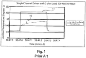
- FIG. 1 is a plot showing the difference between the temperatures 10 sensed by such known temperature sensors in the vicinity of the output driver, and the actual temperature 11 of the driver device, when the output driver is subjected to large pulse power dissipation that causes an SOA violation.
- the actual temperature (11) of the driver device is measured using a thermal IR camera.
- the temperature 10 sensed by the temperature sensor generally differs by at least 50-80 °C from the actual peak junction temperature (11), depending upon power dissipated, e.g., as measured by thermal IR camera. If the absolute maximum junction temperature is 150 °C, which is a typical figure for many output driver devices, an SOA violation is not detected by the temperature sensor as shown in FIG. 1 , even though the actual junction temperature exceeds 150 °C.
- FIG. 2 shows a thermal simulation using finite element analysis (FEA) at 18 W peak power dissipation for an exemplary output driver device with an embedded temperature sensor in the center of the device.
- FEA finite element analysis
- the temperature 21 sensed by the embedded temperature sensor is 113.4 °C, while the maximum actual peak junction temperature 22 is 129.4 °C.
- the temperature 21 sensed by the embedded temperature sensor is at least 16 °C lower than the actual peak junction temperature 22.
- Overcurrent protection is another known technique in amplifiers for protecting the output devices against SOA violations.
- overcurrent protection or current limiting is generally not adequate to protect against SOA violations.
- load current and output voltage can have an out-of-phase relationship or phase delay between them.
- an SOA violation can occur at much lower output current levels that are well below the overcurrent trip threshold if there is a higher voltage across the output driver device.
- US 2004/060026 A1 discloses a thermal protection circuit for an amplifier generating an amplified AC output signal.
- the thermal protection circuit may be powered by an amplifier power supply used to power the output stage.
- the amplifier power supply may be referenced to ground.
- the thermal protection circuit includes a power conditioner for providing regulated power rails to the other components of the thermal protection circuit.
- the regulated power rails may be referenced to the amplified AC output signal.
- US 2004/174218 A1 discloses a method and apparatus for use with a power amplifier to provide a regulated supply to the power amplifier.
- a combination of voltage and current regulation is used.
- voltage regulation is used at high power levels, while current regulation is used at low power levels.
- systems for detecting thermal safe operating area violations for a semiconductor device include a peak power dissipation sensor configured to sense the peak power dissipation in the device and output a signal representative of the peak power dissipation.
- a temperature sensor is configured to sense an average temperature of the device and output a signal representative of the average temperature.
- a maximum allowable peak power dissipation determining circuit is configured to determine a maximum allowable peak power dissipation based at least in part on the signal representative of the average temperature, and to output a signal representative of the maximum allowable peak power dissipation.
- a semiconductor chip that includes a semiconductor device having a peak power dissipation sensor configured to sense the peak power dissipation in the device and output a signal representative of the peak power dissipation.
- a temperature sensor is configured to sense an average temperature of the device and output a signal representative of the average temperature.
- a peak junction temperature computation circuit is configured to receive signals from the peak power dissipation sensor and the temperature sensor, and to generate a signal representative of a peak junction temperature based on the received signals.
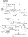
- FIG. 3 is an illustration of a first exemplary block diagram of a peak junction temperature monitoring system 100 for a semiconductor device.
- the system 100 contains a peak power dissipation sensor 110, a temperature sensor 120 and a peak junction temperature computation circuit 130.
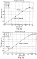
- the temperature sensor 120 is located in the vicinity of the output driver device, but is not embedded into the output driver device. There is no specific, required location for the temperature sensor 120 (i.e., no specific distance from the driver device on a chip) in order to measure an "average temperature," as disclosed herein. Rather, the temperature sensor 120 may be located anywhere such that it can sense a temperature of the device. For example, the temperature sensor 120 may be located on a chip somewhere in the general vicinity of the device. As will be further described herein, in particular with respect to FIGS. 6 and 7a-c , the peak power dissipated (PD_PK) in the driver device may be linearly correlated with the temperature difference ( ⁇ T) between the peak junction temperature (T J ) and the measured average temperature (T AVG ).
- the output (e.g., I DS+_N+ ) of the voltage sensor 114 is a signal representative of the voltage across the device 111 (M N+ ).
- the signal representative of the current through the output device 111, output from the current sensor 112 (I MON_N+ ), and the signal representative of the voltage across the device 111, output from the voltage sensor 114 (I DS_N+ ), are multiplied by a multiplication element 116.
- the resulting signal, output from the multiplication element 116, is a signal (I PD_PK_SENSE ) which is representative of real-time peak power dissipation in the device 111 (M N+ ).
- This signal may be a voltage signal (e.g., V PD_PK_SENSE ), which may be converted into a current signal (e.g., I PD_PK_SENSE ) through a voltage-to-current converter 118.
- the multiplication element 116 may be any known circuit element for multiplying signals, including for example, an electronic mixer for producing an output signal equal to the product of the two input signals.
- the sense signal representative of the peak power dissipation through the device may be, for example, a voltage signal (e.g., signal V PD_PK_SENSE in FIG. 4 ) or a current signal (e.g., I PD_PK_SENSE in FIG. 4 ).
- the sense signal is a voltage signal and the output current is fixed at 1A.
- the sensed voltage increases linearly.
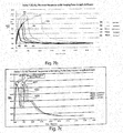
- the data shown in the plot of ⁇ T versus peak power dissipation in FIG. 6 were collected and analyzed for pulse widths ranging from 1 ms to10ms and pulse power ranges from 5W to 20W (see FIGs. 7a-c ).
- the peak power dissipation (PD_PK) was measured using instruments (e.g., voltage and current probes) to measure the peak power dissipation through the output device in real-time.
- the peak junction temperature (T J ) was measured using a thermal camera, and the average temperature (T AVG ) was sensed using a temperature sensor 120 located in the vicinity of the output device 111.
- FIGs. 7a-c are plots showing the temperature difference ( ⁇ T) between the peak junction temperature (T J ) and the sensed average temperature (T AVG ) with differing applied pulse widths and pulse power.
- ⁇ T for each applied 18W peak pulse has substantially the same maximum value 210. Thus, there is substantially no inaccuracy in the measurement of ⁇ T, regardless of the pulse width, for an applied 18 W peak power pulse.
- ⁇ T for each applied 5 W peak pulse has a slightly different maximum value 310.
- the worst case inaccuracy of ⁇ T is about 6.5 °C.
- the maximum difference ( ⁇ T) between the peak junction temperature (T J ) (e.g., as measured by a thermal camera) and the sensed average temperature (T AVG ) (e.g., as sensed using a temperature sensor 120 located in the vicinity of the output device 111) is about 6.5 °C less than the maximum difference ( ⁇ T) between the peak junction temperature (T J ) and the sensed average temperature (T AVG ) for an applied 5 W pulse having a pulse width of 10ms.
- ⁇ T for each applied 18 W peak pulse has multiple maxima, with the maxima for each pulse width having substantially the same maximum value. For example, for the applied 18 W repetitive peak pulse having a 2ms pulse width (line 402), ⁇ T has two maximums 410, both having the same value.
- ⁇ T By measuring the peak dissipated power and the corresponding ⁇ T (e.g., as shown in FIG. 6 ), and/or by measuring ⁇ T in response to a known, applied peak pulse power (e.g., as shown in FIGs. 7a-c ), a relationship between ⁇ T and peak power dissipation may be derived, and ⁇ T can be approximated to be linear with changing peak power dissipation.
- FIG. 9 is a plot 900 showing the computed value of peak junction temperature (T J ) 501 superimposed over the actual peak junction temperature 502, as measured by a thermal camera, resulting from the application of a 14W pulse having a pulse width of 10ms.
- the units of the y-axis of the plot are degrees Celsius (°C) and the units of the x-axis of the plot are milliseconds (ms).
- the computed peak junction temperature 501 is almost identical to the actual, measured peak junction temperature 502 for substantially the entire duration of the application of the 10 ms, 14W pulse (i.e., from 0 to 10.00 ms on the x-axis).
- the signal representative of maximum allowable peak power dissipation (I PD_PK_MAX ) 602 is computed in real time using T AVG , T JMAX and slope K 2 .
- a signal 610 representative of the average temperature (T AVG ) is input from a temperature sensor 120 and is subtracted by a difference element 611 from a signal 612 representative of a maximum allowable peak junction temperature (T JMAX ).
- the signal 612 representative of a maximum allowable peak junction temperature (T JMAX ) may be selectively adjustable to represent any desired maximum peak junction temperature (T JMAX ), for example, by adjusting the current output from the current source 613.
- the output signal 602 of the multiplication element 616 is thus a signal representative of the maximum allowable peak power dissipation, and is input to the comparator 603.
- sensed signals representative of current 620a-d and voltage 621a-d are input into a respective multiplication element 622a-d.
- the output from each multiplication element 622a-d is input into a maximum power dissipation determining circuit 624, which determines which of the input signals represents the largest peak power dissipation through a device, and outputs that signal 601.
- the signal representative of the peak power dissipation 601 is input to the comparator 603.
- the comparator 603 compares the signal representative of the peak power dissipation 601 with the signal representative of the maximum allowable peak power dissipation 602, and outputs a signal 604 indicative of whether a SOA violation has occurred.
- the comparator 603 may output a logical "1" if the signal 601 exceeds the maximum allowable peak power signal 602, thereby indicating that a SOA violation has occurred.
- the comparator 603 may output a logical "0" if the signal 601 does not exceed the maximum allowable peak power signal 602, thereby indicating that no SOA violation has occurred.
- T AVG 25, 85 and 125 °C
- V DS drain-to-source voltage of the output device
- T JMAX maximum allowable peak junction temperature
- I PD_PK_MAX 602decreases with increasing temperature (and increasing sensed T AVG ) and correlates with measured thermal camera data.
- FIG. 12 is a flowchart 1200 illustrating a method of monitoring a peak junction temperature in a semiconductor device, in accordance with the first exemplary system in FIG. 3 . It should be noted that any process descriptions or blocks in flow charts should be understood as representing modules, segments, portions of code, or steps that include one or more instructions for implementing specific logical functions in the process.
- the peak power dissipation in the device 111 is sensed.
- the peak power dissipation may be sensed by a peak power dissipation sensor 110, which may output a signal representative of the peak power dissipation in the device.
- An average temperature of the device 111 is sensed (block 1204) by a temperature sensor 120, which may be located in the vicinity of the device 111.
- the temperature sensor 120 may output a signal representative of the sensed average temperature.
- the temperature sensor 120 may be a non-embedded sensor. Based on the sensed peak power dissipation and average temperature, a signal representative of a peak junction temperature is generated (block 1206).
- the signal representative of a peak junction temperature may be generated by a peak junction temperature computation circuit130 which receives the signal representative of the sensed peak power dissipation and the signal representative of said average temperature, and generates the signal representative of the peak junction temperature based on the received signals.
- the signal representative of the peak junction temperature may be compared with a signal representative of a maximum allowable junction temperature, and it may be determined whether the peak junction temperature exceeds the maximum allowable junction temperature.
- FIG. 13 is a flowchart 1300 illustrating a method of detecting a thermal safe operating area violation in a semiconductor device, in accordance with the second exemplary system in FIG. 10 .
- the peak power dissipation in the device is sensed.
- the sensed peak power dissipation 601 is compared with a signal representative of a maximum allowable peak power dissipation 602 (block 1304).
- the comparison may be performed by a comparator 503, which may generate a signal indicative of a thermal safe operating area violation if the peak power dissipation exceeds the maximum allowable peak power dissipation (block 1306).
Landscapes
- Physics & Mathematics (AREA)
- General Physics & Mathematics (AREA)
- Amplifiers (AREA)
- Power Conversion In General (AREA)
- Testing Of Individual Semiconductor Devices (AREA)
Claims (7)
- Halbleiterchip mit:einer Halbleitervorrichtung,wobei der Halbleiterchip dadurch gekennzeichnet ist, dass er ferner Folgendes umfasst:einen Spitzenverlustleistungssensor (110), der so eingerichtet ist, dass er die Spitzenverlustleistung in der Vorrichtung erfasst und ein Signal (601) ausgibt, das für die Spitzenverlustleistung repräsentativ ist,einen Temperatursensor (120), der so eingerichtet ist, dass er eine Durchschnittstemperatur der Vorrichtung erfasst und ein Signal (610) ausgibt, das für die Durchschnittstemperatur repräsentativ ist,eine eine maximal zulässige Spitzenverlustleistung bestimmende Schaltung, die so eingerichtet ist, dass sie eine maximal zulässige Spitzenverlustleistung wenigstens teilweise beruhend auf dem Signal (610) bestimmt, das für die Durchschnittstemperatur repräsentativ ist, und ein Signal (602) ausgibt, das für die maximal zulässige Spitzenverlustleistung repräsentativ ist, undeinen Komparator (603), der so eingerichtet ist, dass er das Signal (601), das für die Spitzenverlustleistung repräsentativ ist, mit dem Signal (602) vergleicht, das für die maximal zulässige Spitzenverlustleistung repräsentativ ist, und ein Signal (604) ausgibt, das eine Verletzung eines thermisch sicheren Arbeitsbereichs anzeigt, wenn die Spitzenverlustleistung die maximal zulässige Spitzenverlustleistung überschreitet.
- Halbleiterchip nach Anspruch 1,
wobei die die maximal zulässige Spitzenverlustleistung bestimmende Schaltung Folgendes umfasst:ein Differenzelement (611), das so eingerichtet ist, dass es ein Signal (612), das für eine maximal zulässige Spitzensperrschichttemperatur repräsentativ ist, und das Signal (610) empfängt, das für die Durchschnittstemperatur repräsentativ ist, und ein Signal (614) ausgibt, das für eine Differenz zwischen den empfangenen Signalen repräsentativ ist; undein Multiplikationselement (616), das so eingerichtet ist, dass es das Differenzsignal (614) mit einem Signal (615) multipliziert, das für den Kehrwert der Steigung einer Linie repräsentativ ist, die die Differenz zwischen der Spitzensperrschichttemperatur und der Durchschnittstemperatur mit der Spitzenverlustleistung korreliert. - Halbleiterchip nach Anspruch 2, wobei das Signal (602), das für eine maximal zulässige Spitzensperrschichttemperatur repräsentativ ist, gezielt einstellbar ist.
- Halbleiterchip nach Anspruch 1, wobei die die maximal zulässige Spitzenverlustleistung bestimmende Schaltung die maximal zulässige Spitzenverlustleistung in Echtzeit bestimmt.
- Halbleiterchip nach Anspruch 1, ferner mit:mehreren Spitzenverlustleistungssensoren, die jeweils so eingerichtet sind, dass sie die Spitzenverlustleistung in einer jeweiligen Vorrichtung erfassen, undeiner eine maximale Verlustleistung bestimmenden Schaltung (624), die so eingerichtet ist, dass sie von jedem der mehreren Spitzenverlustleistungssensoren ein für die Spitzenverlustleistung repräsentatives Signal empfängt und das für die größte erfasste Spitzenverlustleistung repräsentative Signal an den Komparator (603) ausgibt.
- Halbleiterchip nach Anspruch 1, wobei der Temperatursensor (120) ein nicht eingebetteter Sensor ist.
- Halbleiterchip nach Anspruch 1, wobei die Vorrichtung eine Treibervorrichtung für einen Audioverstärker umfasst.
Applications Claiming Priority (2)
| Application Number | Priority Date | Filing Date | Title |
|---|---|---|---|
| US201161524666P | 2011-08-17 | 2011-08-17 | |
| US13/563,484 US9347835B2 (en) | 2011-08-17 | 2012-07-31 | Systems and methods for peak junction temperature sensing and thermal safe operating area protection |
Publications (3)
| Publication Number | Publication Date |
|---|---|
| EP2559984A2 EP2559984A2 (de) | 2013-02-20 |
| EP2559984A3 EP2559984A3 (de) | 2017-08-02 |
| EP2559984B1 true EP2559984B1 (de) | 2019-03-27 |
Family
ID=47071042
Family Applications (1)
| Application Number | Title | Priority Date | Filing Date |
|---|---|---|---|
| EP12005920.9A Active EP2559984B1 (de) | 2011-08-17 | 2012-08-16 | System für die Spitzenübergangstemperaturerkennung und thermisch sicherer Betriebsbereichsschutz |
Country Status (2)
| Country | Link |
|---|---|
| US (2) | US9347835B2 (de) |
| EP (1) | EP2559984B1 (de) |
Cited By (1)
| Publication number | Priority date | Publication date | Assignee | Title |
|---|---|---|---|---|
| FR3159670A1 (fr) * | 2024-02-28 | 2025-08-29 | Hutchinson | Procede pour determiner un champ de temperature sur une pièce, systeme et nacelle de moteur d’aeronef associes |
Families Citing this family (3)
| Publication number | Priority date | Publication date | Assignee | Title |
|---|---|---|---|---|
| US9268378B2 (en) | 2013-06-28 | 2016-02-23 | Intel Corporation | Techniques and system for managing platform temperature |
| CN107505555B (zh) * | 2017-09-06 | 2019-10-22 | 珠海格力电器股份有限公司 | 一种二极管电学特性曲线绘制方法及测试设备 |
| CN115629285A (zh) * | 2022-10-25 | 2023-01-20 | 重庆长安新能源汽车科技有限公司 | Igbt模块结温的自动测量方法、装置、电子设备及存储介质 |
Family Cites Families (10)
| Publication number | Priority date | Publication date | Assignee | Title |
|---|---|---|---|---|
| US6580318B2 (en) * | 2001-03-08 | 2003-06-17 | Maxim Integrated Products, Inc. | Method and apparatus for protecting radio frequency power amplifiers |
| US6927626B2 (en) * | 2002-09-23 | 2005-08-09 | Harman International Industries, Incorporated | Thermal protection system for an output stage of an amplifier |
| US6897730B2 (en) * | 2003-03-04 | 2005-05-24 | Silicon Laboratories Inc. | Method and apparatus for controlling the output power of a power amplifier |
| US6940981B2 (en) * | 2003-03-12 | 2005-09-06 | Qsc Audio Products, Inc. | Apparatus and method of limiting power applied to a loudspeaker |
| US7030700B2 (en) * | 2004-04-15 | 2006-04-18 | Matsushita Electric Industrial Co., Ltd. | Voltage level detector for power amplifier protection control |
| EP1957992B1 (de) * | 2005-12-06 | 2011-05-25 | Harman International Industries, Incorporated | Diagnosesystem für einen stromumrichter |
| US7449959B2 (en) * | 2007-01-31 | 2008-11-11 | Texas Instruments Incorporated | Methods and apparatus to detect impedance at an amplifier output |
| US7656061B2 (en) * | 2007-10-29 | 2010-02-02 | Bose Corporation | Automatic power source configuration |
| JP2009217809A (ja) * | 2008-02-12 | 2009-09-24 | Seiko Epson Corp | 基準電圧生成回路、集積回路装置および信号処理装置 |
| US8260473B1 (en) * | 2010-04-12 | 2012-09-04 | L-3 Services, Inc. | Managing the operation of a semiconductor device under varying load conditions |
-
2012
- 2012-07-31 US US13/563,484 patent/US9347835B2/en active Active
- 2012-08-16 EP EP12005920.9A patent/EP2559984B1/de active Active
-
2016
- 2016-05-23 US US15/162,325 patent/US10036670B2/en active Active
Non-Patent Citations (1)
| Title |
|---|
| None * |
Cited By (1)
| Publication number | Priority date | Publication date | Assignee | Title |
|---|---|---|---|---|
| FR3159670A1 (fr) * | 2024-02-28 | 2025-08-29 | Hutchinson | Procede pour determiner un champ de temperature sur une pièce, systeme et nacelle de moteur d’aeronef associes |
Also Published As
| Publication number | Publication date |
|---|---|
| US10036670B2 (en) | 2018-07-31 |
| EP2559984A3 (de) | 2017-08-02 |
| EP2559984A2 (de) | 2013-02-20 |
| US20160320246A1 (en) | 2016-11-03 |
| US9347835B2 (en) | 2016-05-24 |
| US20130044786A1 (en) | 2013-02-21 |
Similar Documents
| Publication | Publication Date | Title |
|---|---|---|
| US6888469B2 (en) | Method and apparatus for estimating semiconductor junction temperature | |
| US11215657B2 (en) | Real-time online prediction method for dynamic junction temperature of semiconductor power device | |
| US10036670B2 (en) | Systems and methods for peak junction temperature sensing and thermal safe operating area protection | |
| US6052268A (en) | Electrical apparatus | |
| JP4367339B2 (ja) | 電動機制御装置 | |
| JP5448706B2 (ja) | 電流検出装置及び電流検出方法 | |
| KR100490601B1 (ko) | 이상검지방법 및 보호장치 | |
| US6676287B1 (en) | Direct thermal conductivity measurement technique | |
| EP2325992A1 (de) | Umrichtervorrichtung, umrichtersteuerungssystem, motorsteuerungssystem und verfahren zur steuerung der umrichtervorrichtung | |
| WO2007136854A2 (en) | Sensor adaptors and methods | |
| CN108206511A (zh) | 浪涌电流防止电路及其防止方法、计算机可读取记录介质 | |
| EP2760093B1 (de) | Netzschalter-Fehlerdetektionssystem | |
| EP1939915B1 (de) | Messen einer analogen Spulenspannung und Spulenstrom | |
| EP2027443A2 (de) | Temperatursensoradapter und entsprechende verfahren | |
| US12055583B2 (en) | Method and device for estimating the ageing of an electronic component | |
| TW200518662A (en) | Temperature measurement method and device | |
| Chen et al. | Evaluation of thermal performance of packaged GaN HEMT cascode power switch by transient thermal testing | |
| CN119959720A (zh) | 一种igbt模块的结温检测方法 | |
| US7359172B2 (en) | Junction temperature sensing for MOSFET | |
| US9608558B1 (en) | Calculation of MOSFET switch temperature in motor control | |
| US20050248895A1 (en) | System and method for determining thermal shutdown characteristics | |
| JPH0476799A (ja) | 熱電対温度センサの寿命判定及び寿命予測装置 | |
| EP4357743B1 (de) | Verfahren zur überwachung der zuverlässigkeit eines systems mit elektrischen komponenten | |
| JP2021048305A (ja) | 保護回路、半導体装置及び方法 | |
| JP3132378B2 (ja) | 電線路の温度推定方法 |
Legal Events
| Date | Code | Title | Description |
|---|---|---|---|
| PUAI | Public reference made under article 153(3) epc to a published international application that has entered the european phase |
Free format text: ORIGINAL CODE: 0009012 |
|
| AK | Designated contracting states |
Kind code of ref document: A2 Designated state(s): AL AT BE BG CH CY CZ DE DK EE ES FI FR GB GR HR HU IE IS IT LI LT LU LV MC MK MT NL NO PL PT RO RS SE SI SK SM TR |
|
| AX | Request for extension of the european patent |
Extension state: BA ME |
|
| RAP1 | Party data changed (applicant data changed or rights of an application transferred) |
Owner name: CIRRUS LOGIC |
|
| PUAL | Search report despatched |
Free format text: ORIGINAL CODE: 0009013 |
|
| AK | Designated contracting states |
Kind code of ref document: A3 Designated state(s): AL AT BE BG CH CY CZ DE DK EE ES FI FR GB GR HR HU IE IS IT LI LT LU LV MC MK MT NL NO PL PT RO RS SE SI SK SM TR |
|
| AX | Request for extension of the european patent |
Extension state: BA ME |
|
| RIC1 | Information provided on ipc code assigned before grant |
Ipc: G01K 7/42 20060101AFI20170623BHEP |
|
| STAA | Information on the status of an ep patent application or granted ep patent |
Free format text: STATUS: REQUEST FOR EXAMINATION WAS MADE |
|
| 17P | Request for examination filed |
Effective date: 20180202 |
|
| RBV | Designated contracting states (corrected) |
Designated state(s): AL AT BE BG CH CY CZ DE DK EE ES FI FR GB GR HR HU IE IS IT LI LT LU LV MC MK MT NL NO PL PT RO RS SE SI SK SM TR |
|
| GRAP | Despatch of communication of intention to grant a patent |
Free format text: ORIGINAL CODE: EPIDOSNIGR1 |
|
| STAA | Information on the status of an ep patent application or granted ep patent |
Free format text: STATUS: GRANT OF PATENT IS INTENDED |
|
| INTG | Intention to grant announced |
Effective date: 20181025 |
|
| GRAS | Grant fee paid |
Free format text: ORIGINAL CODE: EPIDOSNIGR3 |
|
| GRAA | (expected) grant |
Free format text: ORIGINAL CODE: 0009210 |
|
| STAA | Information on the status of an ep patent application or granted ep patent |
Free format text: STATUS: THE PATENT HAS BEEN GRANTED |
|
| AK | Designated contracting states |
Kind code of ref document: B1 Designated state(s): AL AT BE BG CH CY CZ DE DK EE ES FI FR GB GR HR HU IE IS IT LI LT LU LV MC MK MT NL NO PL PT RO RS SE SI SK SM TR |
|
| REG | Reference to a national code |
Ref country code: GB Ref legal event code: FG4D |
|
| REG | Reference to a national code |
Ref country code: CH Ref legal event code: EP |
|
| REG | Reference to a national code |
Ref country code: AT Ref legal event code: REF Ref document number: 1113652 Country of ref document: AT Kind code of ref document: T Effective date: 20190415 |
|
| REG | Reference to a national code |
Ref country code: IE Ref legal event code: FG4D |
|
| REG | Reference to a national code |
Ref country code: DE Ref legal event code: R096 Ref document number: 602012058187 Country of ref document: DE |
|
| PG25 | Lapsed in a contracting state [announced via postgrant information from national office to epo] |
Ref country code: LT Free format text: LAPSE BECAUSE OF FAILURE TO SUBMIT A TRANSLATION OF THE DESCRIPTION OR TO PAY THE FEE WITHIN THE PRESCRIBED TIME-LIMIT Effective date: 20190327 Ref country code: NO Free format text: LAPSE BECAUSE OF FAILURE TO SUBMIT A TRANSLATION OF THE DESCRIPTION OR TO PAY THE FEE WITHIN THE PRESCRIBED TIME-LIMIT Effective date: 20190627 Ref country code: SE Free format text: LAPSE BECAUSE OF FAILURE TO SUBMIT A TRANSLATION OF THE DESCRIPTION OR TO PAY THE FEE WITHIN THE PRESCRIBED TIME-LIMIT Effective date: 20190327 Ref country code: FI Free format text: LAPSE BECAUSE OF FAILURE TO SUBMIT A TRANSLATION OF THE DESCRIPTION OR TO PAY THE FEE WITHIN THE PRESCRIBED TIME-LIMIT Effective date: 20190327 |
|
| REG | Reference to a national code |
Ref country code: NL Ref legal event code: MP Effective date: 20190327 |
|
| PG25 | Lapsed in a contracting state [announced via postgrant information from national office to epo] |
Ref country code: BG Free format text: LAPSE BECAUSE OF FAILURE TO SUBMIT A TRANSLATION OF THE DESCRIPTION OR TO PAY THE FEE WITHIN THE PRESCRIBED TIME-LIMIT Effective date: 20190627 Ref country code: GR Free format text: LAPSE BECAUSE OF FAILURE TO SUBMIT A TRANSLATION OF THE DESCRIPTION OR TO PAY THE FEE WITHIN THE PRESCRIBED TIME-LIMIT Effective date: 20190628 Ref country code: RS Free format text: LAPSE BECAUSE OF FAILURE TO SUBMIT A TRANSLATION OF THE DESCRIPTION OR TO PAY THE FEE WITHIN THE PRESCRIBED TIME-LIMIT Effective date: 20190327 Ref country code: LV Free format text: LAPSE BECAUSE OF FAILURE TO SUBMIT A TRANSLATION OF THE DESCRIPTION OR TO PAY THE FEE WITHIN THE PRESCRIBED TIME-LIMIT Effective date: 20190327 Ref country code: HR Free format text: LAPSE BECAUSE OF FAILURE TO SUBMIT A TRANSLATION OF THE DESCRIPTION OR TO PAY THE FEE WITHIN THE PRESCRIBED TIME-LIMIT Effective date: 20190327 Ref country code: NL Free format text: LAPSE BECAUSE OF FAILURE TO SUBMIT A TRANSLATION OF THE DESCRIPTION OR TO PAY THE FEE WITHIN THE PRESCRIBED TIME-LIMIT Effective date: 20190327 |
|
| REG | Reference to a national code |
Ref country code: AT Ref legal event code: MK05 Ref document number: 1113652 Country of ref document: AT Kind code of ref document: T Effective date: 20190327 |
|
| PG25 | Lapsed in a contracting state [announced via postgrant information from national office to epo] |
Ref country code: RO Free format text: LAPSE BECAUSE OF FAILURE TO SUBMIT A TRANSLATION OF THE DESCRIPTION OR TO PAY THE FEE WITHIN THE PRESCRIBED TIME-LIMIT Effective date: 20190327 Ref country code: IT Free format text: LAPSE BECAUSE OF FAILURE TO SUBMIT A TRANSLATION OF THE DESCRIPTION OR TO PAY THE FEE WITHIN THE PRESCRIBED TIME-LIMIT Effective date: 20190327 Ref country code: SK Free format text: LAPSE BECAUSE OF FAILURE TO SUBMIT A TRANSLATION OF THE DESCRIPTION OR TO PAY THE FEE WITHIN THE PRESCRIBED TIME-LIMIT Effective date: 20190327 Ref country code: CZ Free format text: LAPSE BECAUSE OF FAILURE TO SUBMIT A TRANSLATION OF THE DESCRIPTION OR TO PAY THE FEE WITHIN THE PRESCRIBED TIME-LIMIT Effective date: 20190327 Ref country code: AL Free format text: LAPSE BECAUSE OF FAILURE TO SUBMIT A TRANSLATION OF THE DESCRIPTION OR TO PAY THE FEE WITHIN THE PRESCRIBED TIME-LIMIT Effective date: 20190327 Ref country code: PT Free format text: LAPSE BECAUSE OF FAILURE TO SUBMIT A TRANSLATION OF THE DESCRIPTION OR TO PAY THE FEE WITHIN THE PRESCRIBED TIME-LIMIT Effective date: 20190727 Ref country code: ES Free format text: LAPSE BECAUSE OF FAILURE TO SUBMIT A TRANSLATION OF THE DESCRIPTION OR TO PAY THE FEE WITHIN THE PRESCRIBED TIME-LIMIT Effective date: 20190327 Ref country code: EE Free format text: LAPSE BECAUSE OF FAILURE TO SUBMIT A TRANSLATION OF THE DESCRIPTION OR TO PAY THE FEE WITHIN THE PRESCRIBED TIME-LIMIT Effective date: 20190327 |
|
| PG25 | Lapsed in a contracting state [announced via postgrant information from national office to epo] |
Ref country code: SM Free format text: LAPSE BECAUSE OF FAILURE TO SUBMIT A TRANSLATION OF THE DESCRIPTION OR TO PAY THE FEE WITHIN THE PRESCRIBED TIME-LIMIT Effective date: 20190327 Ref country code: PL Free format text: LAPSE BECAUSE OF FAILURE TO SUBMIT A TRANSLATION OF THE DESCRIPTION OR TO PAY THE FEE WITHIN THE PRESCRIBED TIME-LIMIT Effective date: 20190327 |
|
| PG25 | Lapsed in a contracting state [announced via postgrant information from national office to epo] |
Ref country code: IS Free format text: LAPSE BECAUSE OF FAILURE TO SUBMIT A TRANSLATION OF THE DESCRIPTION OR TO PAY THE FEE WITHIN THE PRESCRIBED TIME-LIMIT Effective date: 20190727 Ref country code: AT Free format text: LAPSE BECAUSE OF FAILURE TO SUBMIT A TRANSLATION OF THE DESCRIPTION OR TO PAY THE FEE WITHIN THE PRESCRIBED TIME-LIMIT Effective date: 20190327 |
|
| REG | Reference to a national code |
Ref country code: DE Ref legal event code: R097 Ref document number: 602012058187 Country of ref document: DE |
|
| PG25 | Lapsed in a contracting state [announced via postgrant information from national office to epo] |
Ref country code: DK Free format text: LAPSE BECAUSE OF FAILURE TO SUBMIT A TRANSLATION OF THE DESCRIPTION OR TO PAY THE FEE WITHIN THE PRESCRIBED TIME-LIMIT Effective date: 20190327 |
|
| PLBE | No opposition filed within time limit |
Free format text: ORIGINAL CODE: 0009261 |
|
| STAA | Information on the status of an ep patent application or granted ep patent |
Free format text: STATUS: NO OPPOSITION FILED WITHIN TIME LIMIT |
|
| PG25 | Lapsed in a contracting state [announced via postgrant information from national office to epo] |
Ref country code: SI Free format text: LAPSE BECAUSE OF FAILURE TO SUBMIT A TRANSLATION OF THE DESCRIPTION OR TO PAY THE FEE WITHIN THE PRESCRIBED TIME-LIMIT Effective date: 20190327 |
|
| REG | Reference to a national code |
Ref country code: DE Ref legal event code: R119 Ref document number: 602012058187 Country of ref document: DE |
|
| 26N | No opposition filed |
Effective date: 20200103 |
|
| PG25 | Lapsed in a contracting state [announced via postgrant information from national office to epo] |
Ref country code: TR Free format text: LAPSE BECAUSE OF FAILURE TO SUBMIT A TRANSLATION OF THE DESCRIPTION OR TO PAY THE FEE WITHIN THE PRESCRIBED TIME-LIMIT Effective date: 20190327 |
|
| PG25 | Lapsed in a contracting state [announced via postgrant information from national office to epo] |
Ref country code: LI Free format text: LAPSE BECAUSE OF NON-PAYMENT OF DUE FEES Effective date: 20190831 Ref country code: LU Free format text: LAPSE BECAUSE OF NON-PAYMENT OF DUE FEES Effective date: 20190816 Ref country code: MC Free format text: LAPSE BECAUSE OF FAILURE TO SUBMIT A TRANSLATION OF THE DESCRIPTION OR TO PAY THE FEE WITHIN THE PRESCRIBED TIME-LIMIT Effective date: 20190327 Ref country code: CH Free format text: LAPSE BECAUSE OF NON-PAYMENT OF DUE FEES Effective date: 20190831 |
|
| REG | Reference to a national code |
Ref country code: BE Ref legal event code: MM Effective date: 20190831 |
|
| PG25 | Lapsed in a contracting state [announced via postgrant information from national office to epo] |
Ref country code: DE Free format text: LAPSE BECAUSE OF NON-PAYMENT OF DUE FEES Effective date: 20200303 Ref country code: IE Free format text: LAPSE BECAUSE OF NON-PAYMENT OF DUE FEES Effective date: 20190816 Ref country code: FR Free format text: LAPSE BECAUSE OF NON-PAYMENT OF DUE FEES Effective date: 20190831 |
|
| PG25 | Lapsed in a contracting state [announced via postgrant information from national office to epo] |
Ref country code: BE Free format text: LAPSE BECAUSE OF NON-PAYMENT OF DUE FEES Effective date: 20190831 |
|
| PG25 | Lapsed in a contracting state [announced via postgrant information from national office to epo] |
Ref country code: CY Free format text: LAPSE BECAUSE OF FAILURE TO SUBMIT A TRANSLATION OF THE DESCRIPTION OR TO PAY THE FEE WITHIN THE PRESCRIBED TIME-LIMIT Effective date: 20190327 |
|
| PG25 | Lapsed in a contracting state [announced via postgrant information from national office to epo] |
Ref country code: MT Free format text: LAPSE BECAUSE OF FAILURE TO SUBMIT A TRANSLATION OF THE DESCRIPTION OR TO PAY THE FEE WITHIN THE PRESCRIBED TIME-LIMIT Effective date: 20190327 Ref country code: HU Free format text: LAPSE BECAUSE OF FAILURE TO SUBMIT A TRANSLATION OF THE DESCRIPTION OR TO PAY THE FEE WITHIN THE PRESCRIBED TIME-LIMIT; INVALID AB INITIO Effective date: 20120816 |
|
| PG25 | Lapsed in a contracting state [announced via postgrant information from national office to epo] |
Ref country code: MK Free format text: LAPSE BECAUSE OF FAILURE TO SUBMIT A TRANSLATION OF THE DESCRIPTION OR TO PAY THE FEE WITHIN THE PRESCRIBED TIME-LIMIT Effective date: 20190327 |
|
| P01 | Opt-out of the competence of the unified patent court (upc) registered |
Effective date: 20230308 |
|
| PGFP | Annual fee paid to national office [announced via postgrant information from national office to epo] |
Ref country code: GB Payment date: 20250827 Year of fee payment: 14 |