EP2555094A2 - Structure de panneau à commande tactile présentant un motif factice - Google Patents
Structure de panneau à commande tactile présentant un motif factice Download PDFInfo
- Publication number
- EP2555094A2 EP2555094A2 EP12170041A EP12170041A EP2555094A2 EP 2555094 A2 EP2555094 A2 EP 2555094A2 EP 12170041 A EP12170041 A EP 12170041A EP 12170041 A EP12170041 A EP 12170041A EP 2555094 A2 EP2555094 A2 EP 2555094A2
- Authority
- EP
- European Patent Office
- Prior art keywords
- transparent conductive
- dummy patterns
- touch control
- control panel
- conductive regions
- Prior art date
- Legal status (The legal status is an assumption and is not a legal conclusion. Google has not performed a legal analysis and makes no representation as to the accuracy of the status listed.)
- Withdrawn
Links
Images


Classifications
-
- G—PHYSICS
- G06—COMPUTING; CALCULATING OR COUNTING
- G06F—ELECTRIC DIGITAL DATA PROCESSING
- G06F3/00—Input arrangements for transferring data to be processed into a form capable of being handled by the computer; Output arrangements for transferring data from processing unit to output unit, e.g. interface arrangements
- G06F3/01—Input arrangements or combined input and output arrangements for interaction between user and computer
- G06F3/03—Arrangements for converting the position or the displacement of a member into a coded form
- G06F3/041—Digitisers, e.g. for touch screens or touch pads, characterised by the transducing means
- G06F3/044—Digitisers, e.g. for touch screens or touch pads, characterised by the transducing means by capacitive means
- G06F3/0445—Digitisers, e.g. for touch screens or touch pads, characterised by the transducing means by capacitive means using two or more layers of sensing electrodes, e.g. using two layers of electrodes separated by a dielectric layer
-
- G—PHYSICS
- G06—COMPUTING; CALCULATING OR COUNTING
- G06F—ELECTRIC DIGITAL DATA PROCESSING
- G06F3/00—Input arrangements for transferring data to be processed into a form capable of being handled by the computer; Output arrangements for transferring data from processing unit to output unit, e.g. interface arrangements
- G06F3/01—Input arrangements or combined input and output arrangements for interaction between user and computer
- G06F3/03—Arrangements for converting the position or the displacement of a member into a coded form
- G06F3/041—Digitisers, e.g. for touch screens or touch pads, characterised by the transducing means
- G06F3/044—Digitisers, e.g. for touch screens or touch pads, characterised by the transducing means by capacitive means
- G06F3/0446—Digitisers, e.g. for touch screens or touch pads, characterised by the transducing means by capacitive means using a grid-like structure of electrodes in at least two directions, e.g. using row and column electrodes
-
- H—ELECTRICITY
- H01—ELECTRIC ELEMENTS
- H01B—CABLES; CONDUCTORS; INSULATORS; SELECTION OF MATERIALS FOR THEIR CONDUCTIVE, INSULATING OR DIELECTRIC PROPERTIES
- H01B5/00—Non-insulated conductors or conductive bodies characterised by their form
- H01B5/14—Non-insulated conductors or conductive bodies characterised by their form comprising conductive layers or films on insulating-supports
Definitions
- the present invention relates to a touch control panel, and more particularly to a touch control panel having a dummy pattern structure that can reduce the color difference.
- the touch control panels have display function and are easily to be controlled. In recent years, the touch control panels are widely used in portable or fixed devices such as mobile phones, tablet computers, automated telling machines, automated vending machines, navigation devices, etc. In particular, because the capacitive touch control panel can provide multi-touch control, the resistive touch control panel is becoming increasingly replaced by the capacitive touch control panel.
- the capacitive touch control panel includes two transparent conductive glass plates which sandwiches an optical gel. This capacitive touch control panel is then placed on a display device. A user can touch the surface of the touch control panel at a position corresponding to an image or icon to achieve touch control.
- the conductive glass plates or the conductive films, and the optical gel therebetween can be used as a capacitor to detect a touch position.
- the disadvantage of the conventional touch control panel is that the specific patterns (such as lozenge shape) of the two conductive films, which can define the capacitor, formed by etching can exhibit a color difference, which may affect the image quality. Therefore, a dummy pattern may be used to reduce the optical difference, for example, that disclosed in Taiwanese utility model patent No. M359752 .
- the proposed method still fails to completely solve this problem. Therefore, there is a need for a touch control panel structure having a dummy pattern that can solve the problems of the prior art.
- An objective of the present invention is to provide a touch control panel structure having a dummy pattern, which comprises a substrate, a plurality of first transparent conductive regions, a plurality of first dummy patterns, an insulating layer, a plurality of second transparent conductive regions, and an optical coating layer.
- the first transparent conductive regions and the first dummy patterns are disposed on the substrate, and are covered by the insulating layer.
- the second transparent conductive regions are disposed on the insulating layer and are covered by the optical coating layer.
- the first dummy patterns are respectively aligned with the corresponding second transparent conductive regions, and the first dummy patterns are disconnected from one another.
- the first transparent conductive regions are arranged in a first direction, and the second transparent conductive regions are arranged in a second direction.
- the first direction is, for example, an ordinate direction
- the second direction is, for example, an abscissa direction which is perpendicular to the ordinate direction.
- the display image quality of the touch control panel can be improved.
- Another objective of the present invention is to provide a touch control panel structure having a dummy pattern, which further comprises a plurality of second dummy patterns.
- the second transparent conductive regions and the second dummy patterns are disposed on the insulating layer, and are covered by the optical coating layer.
- the first and second transparent conductive regions are respectively arranged in a first direction and a second direction.
- the first and second dummy patterns are respectively aligned with the corresponding second and first transparent conductive regions.
- the first transparent conductive regions As well as their corresponding second dummy patterns, and the first dummy patterns as well as their corresponding second transparent conductive regions, which can also reduce the color difference so that the first and second transparent conductive regions cannot be visually distinguished.
- the first and second dummy patterns can respectively comprise a plurality of first and second dummy pattern units which are uniformly disposed.
- Each of the first and second dummy pattern units can be in a square, rectangular, or lozenge shape.
- the first dummy patterns or the second dummy patterns can only have one single unit which is in a square, rectangular or lozenge shape.
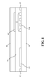
- FIG. 1 is a schematic view showing a touch control panel structure having a dummy pattern according to the present invention
- FIG. 2 is a schematic view showing the first transparent conductive regions and the first dummy patterns according to one embodiment of the present invention
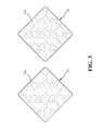
- FIG. 3 is an enlarged view showing the first dummy patterns according to an embodiment of the present invention.
- FIG. 4 is a schematic view showing a touch control panel structure according to another embodiment of the present invention.
- FIG. 5 is a schematic view showing a touch control panel structure according to another embodiment of the present invention.
- FIG. 1 is a schematic view showing a touch control panel structure having a dummy pattern according to the present invention.
- the touch control panel structure comprises a substrate 10, a mask layer 12, a plurality of a first transparent conductive regions 20, a plurality of first dummy patterns 22, an insulating layer 30, a plurality of second transparent conductive regions 40, a plurality of second dummy patterns 42, and an optical coating layer 50 for reducing a visual distinction between the first and second transparent conductive regions.
- the transmitted light can be less affected by the first and second transparent conductive regions, and thereby the display image quality can be improved.
- the substrate 10 is transparent.
- the mask layer 12 is made of an opaque material, for example a black material.
- the mask layer 12 can block light emitted from a display device (not shown) underneath the substrate 10.
- the mask layer 12 has a masking pattern through which the substrate 10 is partially exposed.
- the first transparent conductive layer 20 and the first dummy patterns 22 are made of a transparent conductive material, such as indium tin oxide (ITO) or aluminum zinc oxide (AZO).
- the first transparent conductive regions 20 are disposed on one part of the substrate 10.
- the first dummy patterns 22 are disposed on another part of the substrate 10.
- the first transparent conductive regions 20 are arranged in a first direction, such as in an ordinate direction.
- Each first transparent conductive region comprises a plurality of the first transparent conductive units which are, for example, in a rectangular, square or lozenge shape, and each first transparent conductive unit is connected at two diagonally opposite corners thereof to an adjacent first transparent conductive unit.
- the first transparent conductive regions 20 are, for example, in a square shape, and the first dummy patterns 22 are not connected one another.
- Each first dummy pattern 22 comprise a plurality of first dummy pattern units 22a which are, for example, in a rectangular, square, lozenge triangular, polygonal or irregular shape.
- FIG. 3 is an enlarged view of the first dummy pattern, in which the first dummy pattern units 22a are exemplarily in a square shape.
- the insulating layer 30 is transparent and electrically insulating.
- the insulating layer 30 covers the mask layer 12, the first transparent conductive regions 20, the first dummy patterns 22, and the substrate 10 uncovered by the mask layer 12, the first transparent conductive regions 20 and the first dummy patterns 22.
- the second transparent conductive regions 40 are made of the same transparent conductive material as that of the first transparent conductive regions 20.
- the second transparent conductive regions 40 are disposed on a portion of the insulating layer 30, and are arranged in a second direction different from the first direction, and the second direction is, for example, the abscissa direction.
- each second transparent conductive region 40 comprises a plurality of the second transparent conductive units which are, for example, in a rectangular, square or lozenge shape, and each second transparent conductive unit is connected at two diagonally opposite corners thereof to an adjacent second transparent conductive unit.
- each second transparent conductive region 40 is aligned vertically with the corresponding first dummy pattern 22.
- an angle defined between the first direction and the second direction is between 30 degrees and 90 degrees.
- the optical coating layer 50 is transparent and electrically insulating.
- the optical coating layer 50 covers the second transparent conductive regions 40 and the insulating layer 30 uncovered by the second transparent conductive regions 40.
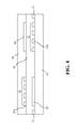
- FIG. 4 is a schematic view showing another embodiment of a touch control panel structure of the present invention.
- the touch control panel structure can further comprise a plurality of the second dummy patterns 42 that are made of the same transparent conductive material as that of the second transparent conductive regions 40.
- the second dummy patterns 42 are disposed on a portion of the insulating layer 30, and are covered with the optical coating layer 50.
- Each second dummy pattern 42 is vertically aligned with the corresponding first transparent conductive regions 20.
- Each second dummy pattern 42 comprises a plurality of second dummy pattern units 42a which are in a rectangular, square, lozenge, triangular, polygonal or irregular shape, as the first dummy pattern units 22a.
- FIG. 5 is a schematic view showing a touch control panel structure according to another embodiment of the present invention.
- Each first dummy pattern 22 only has one single first dummy unit 24 which is in a lozenge shape.
- the first dummy pattern 24 is not larger than the second transparent conductive region 40.
- Each second dummy pattern 42 only has one single second dummy unit 44 which is in a lozenge shape that is not larger than the first transparent conductive region 20.
- the feature of the touch control panel structure according to the present invention is that when light is emitted upward from the bottom of the substrate, it can pass through the first dummy pattern and the second transparent conductive regions aligned therewith, so that the transmitted light can be less affected by the second transparent conductive regions, and thereby the display image quality can be improved.
- the other feature of the touch control panel structure according to the present invention is that because the first and second dummy patterns are respectively in alignment with the first and second transparent conductive regions, the first and second transparent conductive regions are visually indistinguishable from each other, and thereby the display image quality can be improved.
Applications Claiming Priority (1)
| Application Number | Priority Date | Filing Date | Title |
|---|---|---|---|
| TW100128032A TWI451300B (zh) | 2011-08-05 | 2011-08-05 | A dummy pattern of touch panel structure |
Publications (2)
| Publication Number | Publication Date |
|---|---|
| EP2555094A2 true EP2555094A2 (fr) | 2013-02-06 |
| EP2555094A3 EP2555094A3 (fr) | 2016-06-22 |
Family
ID=46261926
Family Applications (1)
| Application Number | Title | Priority Date | Filing Date |
|---|---|---|---|
| EP12170041.3A Withdrawn EP2555094A3 (fr) | 2011-08-05 | 2012-05-30 | Structure de panneau à commande tactile présentant un motif factice |
Country Status (5)
| Country | Link |
|---|---|
| EP (1) | EP2555094A3 (fr) |
| JP (2) | JP2013038067A (fr) |
| KR (1) | KR20130017071A (fr) |
| SG (1) | SG187315A1 (fr) |
| TW (1) | TWI451300B (fr) |
Cited By (1)
| Publication number | Priority date | Publication date | Assignee | Title |
|---|---|---|---|---|
| US20140307178A1 (en) * | 2013-04-12 | 2014-10-16 | Shenzhen O-Film Tech Co., Ltd | Touch screen sensing module, manufacturing method thereof and display device |
Families Citing this family (7)
| Publication number | Priority date | Publication date | Assignee | Title |
|---|---|---|---|---|
| JP6674257B2 (ja) * | 2013-02-27 | 2020-04-01 | ミラエナノテック カンパニー リミテッド | 静電容量方式タッチスクリーンのためのダミーパターンを使用するタッチパッドの構造 |
| WO2014133347A1 (fr) * | 2013-02-27 | 2014-09-04 | 미래나노텍 주식회사 | Structure d'une touche d'effleurement utilisant un motif factice pour un écran tactile de type capacitif |
| JP6131071B2 (ja) * | 2013-03-14 | 2017-05-17 | 株式会社ジャパンディスプレイ | タッチパネル内蔵型表示装置 |
| KR102175821B1 (ko) | 2013-11-07 | 2020-11-09 | 삼성디스플레이 주식회사 | 이미지를 갖는 접촉 위치 감지 패널 |
| KR102521876B1 (ko) * | 2016-04-12 | 2023-04-18 | 삼성디스플레이 주식회사 | 전자 장치 및 이의 제조 방법 |
| TWI649599B (zh) | 2017-08-31 | 2019-02-01 | 友達光電股份有限公司 | 顯示裝置 |
| CN109871157B (zh) * | 2019-02-01 | 2022-07-19 | 云谷(固安)科技有限公司 | 触控显示面板和触控显示装置 |
Family Cites Families (6)
| Publication number | Priority date | Publication date | Assignee | Title |
|---|---|---|---|---|
| JP4945483B2 (ja) * | 2008-02-27 | 2012-06-06 | 株式会社 日立ディスプレイズ | 表示パネル |
| KR20100006987A (ko) * | 2008-07-11 | 2010-01-22 | 삼성모바일디스플레이주식회사 | 터치 스크린 패널 및 그 제조방법 |
| US20100045625A1 (en) * | 2008-08-21 | 2010-02-25 | Tpo Displays Corp. | Touch panel and system for displaying images utilizing the same |
| CN101393502B (zh) * | 2008-10-31 | 2012-03-07 | 敦泰科技有限公司 | 互电容式触摸屏及组合式互电容触摸屏 |
| CN101943975B (zh) * | 2009-07-09 | 2015-12-16 | 敦泰科技有限公司 | 超薄型互电容触摸屏及组合式超薄型触摸屏 |
| JP5372697B2 (ja) * | 2009-10-21 | 2013-12-18 | 京セラディスプレイ株式会社 | 投影型静電容量タッチパネルの製造方法 |
-
2011
- 2011-08-05 TW TW100128032A patent/TWI451300B/zh not_active IP Right Cessation
-
2012
- 2012-05-30 EP EP12170041.3A patent/EP2555094A3/fr not_active Withdrawn
- 2012-06-07 JP JP2012129859A patent/JP2013038067A/ja active Pending
- 2012-06-21 SG SG2012046371A patent/SG187315A1/en unknown
- 2012-06-22 KR KR1020120067112A patent/KR20130017071A/ko not_active Application Discontinuation
-
2013
- 2013-12-02 JP JP2013006839U patent/JP3189018U/ja not_active Expired - Fee Related
Cited By (1)
| Publication number | Priority date | Publication date | Assignee | Title |
|---|---|---|---|---|
| US20140307178A1 (en) * | 2013-04-12 | 2014-10-16 | Shenzhen O-Film Tech Co., Ltd | Touch screen sensing module, manufacturing method thereof and display device |
Also Published As
| Publication number | Publication date |
|---|---|
| KR20130017071A (ko) | 2013-02-19 |
| EP2555094A3 (fr) | 2016-06-22 |
| JP3189018U (ja) | 2014-02-20 |
| SG187315A1 (en) | 2013-02-28 |
| JP2013038067A (ja) | 2013-02-21 |
| TW201308142A (zh) | 2013-02-16 |
| TWI451300B (zh) | 2014-09-01 |
Similar Documents
| Publication | Publication Date | Title |
|---|---|---|
| EP2555094A2 (fr) | Structure de panneau à commande tactile présentant un motif factice | |
| JP6702890B2 (ja) | アレイ基板及びその作成方法と駆動方法、表示装置 | |
| EP3153946B1 (fr) | Écran tactile encastré et dispositif d'affichage | |
| CN102841716B (zh) | 一种电容式内嵌触摸屏及显示装置 | |
| US10871839B2 (en) | Color filter substrate, array substrate and display device | |
| CN102749747B (zh) | 触控显示面板及其制造方法 | |
| US10067614B2 (en) | In-cell touch panel and display device | |
| EP2613235B1 (fr) | Panneau tactile et son procédé de fabrication | |
| EP3153953A1 (fr) | Écran tactile encastré et appareil d'affichage | |
| EP3667476A1 (fr) | Panneau tactile, son procédé de fabrication et dispositif d'affichage tactile | |
| US20110134075A1 (en) | Touch panel, display, and electronic device | |
| EP2876531A1 (fr) | Écran tactile capacitif intégral non chevauché à couche ito (oxyde d'indium-étain) et procédé de fabrication associé | |
| US20130293487A1 (en) | Touch panel | |
| WO2015135289A1 (fr) | Écran tactile incorporé et dispositif d'affichage | |
| CN105138191A (zh) | 一种触控显示装置及其制作方法 | |
| US20130154954A1 (en) | Touch Control Panel Structure Having A Dummy Pattern | |
| CN104461145A (zh) | 一种触摸屏及其制造方法 | |
| CN110825276A (zh) | 触摸指纹复合传感器和包括触摸指纹复合传感器的电子装置 | |
| US20170308194A1 (en) | Touch Sensor Mesh Designs | |
| CN104793797A (zh) | 触摸显示屏及其制作方法、显示装置 | |
| CN109814758B (zh) | 触控基板、触控驱动方法和电子装置 | |
| CN104076991B (zh) | 一种触摸屏、触摸显示面板和触摸显示装置 | |
| CN102955593B (zh) | 具虚设图案的触控面板结构 | |
| CN108920033B (zh) | 一种内嵌式触摸屏及显示装置 | |
| CN111025787A (zh) | 显示面板及显示装置 |
Legal Events
| Date | Code | Title | Description |
|---|---|---|---|
| PUAI | Public reference made under article 153(3) epc to a published international application that has entered the european phase |
Free format text: ORIGINAL CODE: 0009012 |
|
| 17P | Request for examination filed |
Effective date: 20121108 |
|
| AK | Designated contracting states |
Kind code of ref document: A2 Designated state(s): AL AT BE BG CH CY CZ DE DK EE ES FI FR GB GR HR HU IE IS IT LI LT LU LV MC MK MT NL NO PL PT RO RS SE SI SK SM TR |
|
| AX | Request for extension of the european patent |
Extension state: BA ME |
|
| PUAL | Search report despatched |
Free format text: ORIGINAL CODE: 0009013 |
|
| AK | Designated contracting states |
Kind code of ref document: A3 Designated state(s): AL AT BE BG CH CY CZ DE DK EE ES FI FR GB GR HR HU IE IS IT LI LT LU LV MC MK MT NL NO PL PT RO RS SE SI SK SM TR |
|
| AX | Request for extension of the european patent |
Extension state: BA ME |
|
| RIC1 | Information provided on ipc code assigned before grant |
Ipc: G06F 3/044 20060101AFI20160518BHEP |
|
| STAA | Information on the status of an ep patent application or granted ep patent |
Free format text: STATUS: THE APPLICATION IS DEEMED TO BE WITHDRAWN |
|
| 18D | Application deemed to be withdrawn |
Effective date: 20161223 |