EP2555052A1 - Photomask unit and method of manufacturing same - Google Patents
Photomask unit and method of manufacturing same Download PDFInfo
- Publication number
- EP2555052A1 EP2555052A1 EP11765309A EP11765309A EP2555052A1 EP 2555052 A1 EP2555052 A1 EP 2555052A1 EP 11765309 A EP11765309 A EP 11765309A EP 11765309 A EP11765309 A EP 11765309A EP 2555052 A1 EP2555052 A1 EP 2555052A1
- Authority
- EP
- European Patent Office
- Prior art keywords
- photomask
- onto
- stage
- pellicle
- fixed
- Prior art date
- Legal status (The legal status is an assumption and is not a legal conclusion. Google has not performed a legal analysis and makes no representation as to the accuracy of the status listed.)
- Granted
Links
Images


Classifications
-
- G—PHYSICS
- G03—PHOTOGRAPHY; CINEMATOGRAPHY; ANALOGOUS TECHNIQUES USING WAVES OTHER THAN OPTICAL WAVES; ELECTROGRAPHY; HOLOGRAPHY
- G03F—PHOTOMECHANICAL PRODUCTION OF TEXTURED OR PATTERNED SURFACES, e.g. FOR PRINTING, FOR PROCESSING OF SEMICONDUCTOR DEVICES; MATERIALS THEREFOR; ORIGINALS THEREFOR; APPARATUS SPECIALLY ADAPTED THEREFOR
- G03F1/00—Originals for photomechanical production of textured or patterned surfaces, e.g., masks, photo-masks, reticles; Mask blanks or pellicles therefor; Containers specially adapted therefor; Preparation thereof
- G03F1/22—Masks or mask blanks for imaging by radiation of 100nm or shorter wavelength, e.g. X-ray masks, extreme ultraviolet [EUV] masks; Preparation thereof
- G03F1/24—Reflection masks; Preparation thereof
-
- G—PHYSICS
- G03—PHOTOGRAPHY; CINEMATOGRAPHY; ANALOGOUS TECHNIQUES USING WAVES OTHER THAN OPTICAL WAVES; ELECTROGRAPHY; HOLOGRAPHY
- G03F—PHOTOMECHANICAL PRODUCTION OF TEXTURED OR PATTERNED SURFACES, e.g. FOR PRINTING, FOR PROCESSING OF SEMICONDUCTOR DEVICES; MATERIALS THEREFOR; ORIGINALS THEREFOR; APPARATUS SPECIALLY ADAPTED THEREFOR
- G03F1/00—Originals for photomechanical production of textured or patterned surfaces, e.g., masks, photo-masks, reticles; Mask blanks or pellicles therefor; Containers specially adapted therefor; Preparation thereof
- G03F1/62—Pellicles, e.g. pellicle assemblies, e.g. having membrane on support frame; Preparation thereof
-
- G—PHYSICS
- G03—PHOTOGRAPHY; CINEMATOGRAPHY; ANALOGOUS TECHNIQUES USING WAVES OTHER THAN OPTICAL WAVES; ELECTROGRAPHY; HOLOGRAPHY
- G03F—PHOTOMECHANICAL PRODUCTION OF TEXTURED OR PATTERNED SURFACES, e.g. FOR PRINTING, FOR PROCESSING OF SEMICONDUCTOR DEVICES; MATERIALS THEREFOR; ORIGINALS THEREFOR; APPARATUS SPECIALLY ADAPTED THEREFOR
- G03F1/00—Originals for photomechanical production of textured or patterned surfaces, e.g., masks, photo-masks, reticles; Mask blanks or pellicles therefor; Containers specially adapted therefor; Preparation thereof
- G03F1/62—Pellicles, e.g. pellicle assemblies, e.g. having membrane on support frame; Preparation thereof
- G03F1/64—Pellicles, e.g. pellicle assemblies, e.g. having membrane on support frame; Preparation thereof characterised by the frames, e.g. structure or material, including bonding means therefor
-
- H—ELECTRICITY
- H10—SEMICONDUCTOR DEVICES; ELECTRIC SOLID-STATE DEVICES NOT OTHERWISE PROVIDED FOR
- H10P—GENERIC PROCESSES OR APPARATUS FOR THE MANUFACTURE OR TREATMENT OF DEVICES COVERED BY CLASS H10
- H10P76/00—Manufacture or treatment of masks on semiconductor bodies, e.g. by lithography or photolithography
- H10P76/20—Manufacture or treatment of masks on semiconductor bodies, e.g. by lithography or photolithography of masks comprising organic materials
- H10P76/204—Manufacture or treatment of masks on semiconductor bodies, e.g. by lithography or photolithography of masks comprising organic materials of organic photoresist masks
- H10P76/2041—Photolithographic processes
-
- Y—GENERAL TAGGING OF NEW TECHNOLOGICAL DEVELOPMENTS; GENERAL TAGGING OF CROSS-SECTIONAL TECHNOLOGIES SPANNING OVER SEVERAL SECTIONS OF THE IPC; TECHNICAL SUBJECTS COVERED BY FORMER USPC CROSS-REFERENCE ART COLLECTIONS [XRACs] AND DIGESTS
- Y10—TECHNICAL SUBJECTS COVERED BY FORMER USPC
- Y10T—TECHNICAL SUBJECTS COVERED BY FORMER US CLASSIFICATION
- Y10T29/00—Metal working
- Y10T29/49—Method of mechanical manufacture
- Y10T29/49826—Assembling or joining
Definitions
- the present invention relates to a method for fabricating a photomask unit comprising a pellicle for lithography for use as a dustproof cover for an exposure stencil such as a photomask, a reticle or the like (hereinafter collectively referred to as "photomask” in this specification) when a semiconductor device such as a large-scale integrated circuit, a very-large-scale integrated circuit (LSI) or the like, or a liquid crystal display panel is to be manufactured and a photomask, and particularly relates to a photomask unit and a method for fabricating a photomask unit suitable for exposing a photoresist film to light having an extremely short wavelength, thereby forming a microscopic pattern.
- photomask a pellicle for lithography for use as a dustproof cover for an exposure stencil such as a photomask, a reticle or the like
- a photoresist film formed on a semiconductor wafer or a liquid crystal display panel mother substrate is irradiated with an exposure light via a photomask, whereby a pattern of the photomask is transferred onto the semiconductor device or the liquid crystal display panel mother substrate so that a pattern of the semiconductor device or the liquid crystal display panel is formed.
- the operation of exposing the semiconductor wafer or the liquid crystal display panel mother substrate is generally conducted in a clean room.
- the operation of exposing the semiconductor wafer or the liquid crystal display panel mother substrate is usually conducted with a dust proof cover, called a pellicle, and having a high transmittance with respect to the exposure light, mounted on the surface of the photomask.
- a pellicle is manufactured by adhering a pellicle membrane made of a material having a high transmittance with respect to an exposure light, such as a cellulose based resin like nitrocellulose or cellulose acetate, fluoride resin or the like, to one surface of a pellicle frame made of aluminum, stainless steel, polyethylene or the like by applying a good solvent for the material of the pellicle membrane onto the one surface of the pellicle frame and adhering the air-dried pellicle membrane onto the one surface of the pellicle frame, or adhering the pellicle membrane onto the one surface of the pellicle frame using an adhesive agent such as acrylic resin, epoxy resin, fluorine resin or the like, and then forming an agglutinant layer composed of polybutene resin, polyvinyl acetate resin, acrylic resin, silicone resin or the like and adapted for adhering the photomask, and providing a release layer or a separator for protecting the agglutinant
- Figure 1 is a schematic plan view showing a conventional photomask unit including a photomask and a pellicle attached to the photomask and
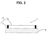
- Figure 2 is a schematic cross sectional view taken along a line A-A in Figure 1 .
- a photomask unit 1 includes a photomask 2 and a pellicle 5 including a pellicle membrane 6 and a frame-like shaped pellicle frame 7 wherein a region of the pellicle membrane 6 in the vicinity of side portions thereof is adhered to the one surface of the pellicle frame 7 and the other surface of the pellicle frame 7 is fixed onto the surface of the photomask 2 by an agglutinant agent (not shown) comprising an organic material.
- a semiconductor device and a liquid crystal display panel are recently required to have higher integration density and a more microscopic pattern and at present, it is put into practical use to form a microscopic pattern of about 45 nm on a photoresist film. It is possible to form a microscopic pattern of about 45 nm on a photoresist film by improving a conventional exposure technique using an eximer laser beam, for example, an immersion exposure technique including steps of filling a space between the semiconductor wafer or the liquid crystal display panel mother substrate and a projector lens with liquid such as ultrapure water and exposing the photoresist film to an argon fluoride (ArF) excimer laser beam, a double exposure technique or the like.
- argon fluoride ArF
- next-generation type semiconductor device or a next-generation type liquid crystal display panel it is required for a next-generation type semiconductor device or a next-generation type liquid crystal display panel to form a more microscopic pattern of 32 nm or smaller on a photoresist film and it is impossible to form a microscopic pattern of 32 nm or smaller on a photoresist film by improving a conventional exposure technique using an excimer laser beam.
- an EUV (Extreme Ultra Violet) exposure technique using an EUV (Extreme Ultra Violet) light whose dominant wavelength is 13.5 nm is considered a strong favorite as a method for forming a pattern of 32 nm or smaller.
- a pellicle frame to which a pellicle membrane is attached is mounted on a photomask via an agglutinant agent containing an organic material.
- an EUV exposure technique it is necessary to keep an exposure chamber to be vacuum.
- a photomask is required to have a high flatness but in the case of mounting a pellicle frame on a photomask using an agglutinant agent containing an organic material, the flatness of a photomask is lowered.
- Another object of the present invention is to provide a method for fabricating a photomask unit comprising a pellicle and a photomask onto which the pellicle is attached, the photomask unit being suitable for forming a microscopic pattern of 32 nm or smaller on a photoresist film using an EUV exposure technique and being able to reliably prevent the flatness of a photomask from being lowered.
- a photomask unit comprising a pellicle membrane, a pellicle frame having a frame-like shape onto one surface of which a region of the pellicle membrane in the vicinity of side portions of the pellicle membrane is attached, a photomask, and a stage onto one surface of which the photomask and the pellicle frame are fixed, wherein the pellicle frame is fixed onto the stage at a region outside of a region of the stage onto which the photomask is fixed.
- the pellicle frame onto the one surface of which the region of the pellicle membrane in the vicinity of side portions of the pellicle membrane is attached is fixed onto the stage at a region outside of a region of the stage onto which the photomask is fixed and the region of the stage onto which the pellicle frame is fixed is apart from an exposure pattern portion where the photomask formed with a pattern and exposed to light is located, when a microscopic pattern of 32 nm or smaller is formed on a photoresist film using the EUV exposure technique while keeping an exposure chamber to be vacuum, even if an outgas is generated from the agglutinant agent containing an organic material, it is possible to efficiently prevent the exposure operation of the photoresist film formed on a semiconductor device or the liquid crystal display panel from being subject to adverse effect.
- the pellicle frame is fixed onto the stage at a region outside of a region of the stage onto which the photomask is fixed and is not fixed onto the photomask unlike the conventional photomask unit, it is possible to reliably prevent the flatness of the photomask from being lowered.
- the pellicle frame it is preferable for the pellicle frame to be made of metal.
- the pellicle frame is fixed by an electrostatic chuck onto the one surface of the stage.
- the pellicle frame is fixed by an electrostatic chuck onto the one surface of the stage, it is possible to reliably prevent an outgas from being generated from a portion where the pellicle frame is fixed on the stage, when a microscopic pattern of 32 nm or smaller is formed on a photoresist film using the EUV exposure technique while keeping an exposure chamber to be vacuum.
- the pellicle frame is fixed by a mechanical means onto the one surface of the stage.
- the pellicle frame is fixed by a mechanical means such as clamps, threads or the like onto the one surface of the stage, it is possible to reliably prevent an outgas from being generated from a portion where the pellicle frame is fixed on the stage, when a microscopic pattern of 32 nm or smaller is formed on a photoresist film using the EUV exposure technique while keeping an exposure chamber to be vacuum.
- the pellicle frame is fixed by an agglutinant agent onto the one surface of the stage.
- a method for fabricating a photomask unit comprising a pellicle membrane, a pellicle frame having a frame-like shape and onto the one surface of which a region of the pellicle membrane in the vicinity of side portions of the pellicle membrane is attached, a photomask and a stage onto the one surface of which the photomask and the pellicle frame are to be fixed, the method for fabricating a photomask unit comprising steps of fixing the photomask onto the one surface of the stage and fixing the other surface of the pellicle frame onto the one surface of the stage at a region outside of a region of the one surface of the stage onto which the photomask is fixed.
- the pellicle frame onto the one surface of which the region of the pellicle membrane in the vicinity of side portions of the pellicle membrane is attached is fixed onto the stage at a region outside of a portion of the stage onto which the photomask is fixed and the portion of the stage onto which the pellicle frame is fixed is apart from an exposure pattern portion where the photomask formed with a pattern and exposed to light is located, when a microscopic pattern of 32 nm or smaller is formed on a photoresist film using the EUV exposure technique while keeping an exposure chamber to be vacuum, even if an outgas is generated from the agglutinant agent containing an organic material, it is possible to efficiently prevent the exposure operation of the photoresist film formed on a semiconductor device or a liquid crystal display panel from being subject to adverse effect.
- the pellicle frame is fixed onto the stage at a region outside of a region of the stage onto which the photomask is fixed and is not fixed onto the photomask unlike the conventional photomask unit, it is possible to reliably prevent the flatness of the photomask from being lowered.
- the pellicle frame is fixed by an electrostatic chuck onto the one surface of the stage.
- the pellicle frame is fixed by an electrostatic chuck onto the one surface of the stage, it is possible to reliably prevent an outgas from being generated from a portion where the pellicle frame is fixed onto the stage, when a microscopic pattern of 32 nm or smaller is formed on a photoresist film using the EUV exposure technique while keeping an exposure chamber to be vacuum.
- the pellicle frame is fixed by a mechanical means onto the one surface of the stage.
- the pellicle frame is fixed by a mechanical means such as a clamp, a thread or the like onto the one surface of the stage, it is possible to reliably prevent an outgas from being generated from a portion where the pellicle frame is fixed onto the stage, when a microscopic pattern of 32 nm or smaller is formed on a photoresist film using the EUV exposure technique while keeping an exposure chamber to be vacuum.
- the pellicle frame is fixed by an agglutinant agent onto the one surface of the stage.
- a photomask unit comprising a photomask and a pellicle attached onto the photomask, the photomask unit being suitable for forming a microscopic pattern of 32 nm or smaller on a photoresist film using an EUV exposure technique and being able to reliably prevent the flatness of a photomask from being lowered.
- a method for fabricating a photomask unit comprising a photomask and a pellicle attached onto the photomask, the photomask unit being suitable for forming a microscopic pattern of 32 nm or smaller on a photoresist film using an EUV exposure technique and being able to reliably prevent the flatness of a photomask from being lowered.
- Figure 1 is a schematic plan view showing a conventional photomask unit including a photomask and a pellicle attached onto the photomask.
- Figure 2 is a schematic cross sectional view taken along a line A-A in Figure 1 .
- Figure 3 is a schematic perspective plan view showing a photomask unit including a photomask and a pellicle attached onto the photomask, which is a preferred embodiment of the present invention.
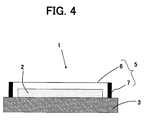
- Figure 4 is a schematic cross sectional view taken along a line B-B in Figure 3 .
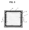
- Figure 5 is a schematic perspective plan view showing a photomask unit including a pellicle attached onto the photomask, which is another preferred embodiment of the present invention.
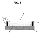
- Figure 6 is a schematic cross sectional view taken along a line C-C in Figure 5 .
- Figure 3 is a schematic perspective plan view showing a photomask unit including a photomask and a pellicle attached onto the photomask, which is a preferred embodiment of the present invention and
- Figure 4 is a schematic cross sectional view taken along a line B-B in Figure 3 .
- a photomask unit 1 includes a photomask 2, a photomask stage 3 onto which the photomask 2 is to be fixed, a pellicle membrane 6 and a pellicle frame 7 having a frame-like shape and attached with the pellicle membrane 6 on the one surface thereof, and a pellicle 5 is constituted by the pellicle membrane 6 and the pellicle frame 7.
- the pellicle frame 7 is made of aluminum.
- the size of the pellicle frame 7 is larger than that of the photomask 2 and the pellicle frame 7 is fixed onto the photomask stage 3 at a region outside of a region of the photomask stage 3 onto which the photomask 2 is fixed.
- the photomask 2 is accommodated in a closed space defined by the pellicle membrane 6 and the pellicle frame 7.
- the photomask 2 is fixed by an electrostatic chuck (not shown) onto the photomask stage 3.
- the pellicle frame 7 is also fixed by an electrostatic chuck onto the photomask stage 3
- the pellicle frame 7 may be fixed onto the photomask stage 3 using a mechanical means such as a clamp, a thread or the like.
- the pellicle frame 7 may be fixed onto the photomask stage 3 using an agglutinant agent containing an organic material such as a silicone agglutinant agent.
- the thus fabricated photomask unit 1 is set in an exposure chamber (not shown). Then, an exposure light is projected via the photomask 2 onto a photoresist film coated on a semiconductor wafer or a liquid crystal display panel mother substrate and a pattern of the photomask 2 is transferred onto the photoresist film, thereby forming a pattern of a semiconductor wafer or the liquid crystal display panel mother substrate.
- the photomask 2 and the pellicle frame 7 are fixed onto the photomask stage 3 by the electrostatic chuck and the size of the pellicle frame 7 is larger than that of the photomask 2.
- the pellicle frame 7 is fixed by an electrostatic chuck onto the photomask stage 3 at a region outside of a region of the photomask stage 3 onto which the photomask 2 is fixed. Therefore, even when the photoresist film of the semiconductor wafer or the liquid crystal display panel mother substrate (not shown) is exposed to an EUV light while keeping an exposure chamber to be vacuum, an outgas cannot be generated. Accordingly, even in the case of forming a microscopic pattern of 32 nm or smaller on the photoresist film while keeping an exposure chamber to be vacuum, it is possible to improve the yield ratio of the semiconductor device or the liquid crystal display panel.
- the pellicle frame 7 is fixed onto the photomask stage 3 at a region outside of a region of the photomask stage 3 onto which the photomask 2 is fixed and is not fixed onto the surface of the photomask 2 unlike the conventional photomask unit, it is possible to suppress the lowering of the flatness of the photomask 2 caused by attaching the pellicle 5 to the minimum.
- Figure 5 is a schematic perspective plan view showing a photomask unit including a photomask and a pellicle attached to the photomask stage, which is another preferred embodiment of the present invention and
- Figure 6 is a schematic cross sectional view taken along a line C-C in Figure 5 .
- a photomask unit 1 similarly to the photomask unit 1 according to the previous embodiment, includes a photomask 2, a photomask stage 3 onto the one surface of which the photomask 2 is to be fixed, a pellicle membrane 6 and a frame-like shaped pellicle frame 7 onto which the pellicle membrane 6 is attached, and a pellicle 5 is constituted by the pellicle membrane 6 and the pellicle frame 7.
- the pellicle frame 7 is also made of aluminum.
- the size of the pellicle frame 7 is larger than that of the photomask 2 and the pellicle frame 7 is fixed onto the photomask stage 3 at a region outside of a region of the photomask stage 3 onto which the photomask 2 is fixed.
- the photomask 2 is fixed by an electrostatic chuck onto the photomask stage 3.
- the pellicle frame 7 is fixed onto the photomask stage 3 by a mechanical clamp 9.
- the thus fabricated photomask unit 1 is set in an exposure chamber (not shown). Then, an exposure light is projected via the photomask 2 onto a photoresist film formed on a semiconductor wafer or a liquid crystal display panel mother substrate and a pattern of the photomask 2 is transferred onto the photoresist film, thereby forming a pattern of a semiconductor wafer or a liquid crystal display panel mother substrate.
- the size of the pellicle frame 7 is larger than that of the photomask 2 and the pellicle frame 7 is fixed by mechanical clamp 9 onto the photomask stage 3 at a region outside of a region of the photomask stage 3 onto which the photomask 2 is fixed. Therefore, even when the photoresist film of the semiconductor wafer or the liquid crystal display panel mother substrate (not shown) is exposed to an EUV light while keeping an exposure chamber to be vacuum, an outgas cannot be generated. Thus, even in the case of forming a microscopic pattern of 32 nm or smaller while keeping an exposure chamber to be vacuum, it is possible to improve the yield ratio of the semiconductor device or the liquid crystal display panel.
- the pellicle frame 7 is fixed onto the photomask stage 3 at a region outside of a region onto which the photomask 2 is fixed and is not fixed onto the surface of the photomask 2 unlike the conventional photomask unit, it is possible to suppress the lowering of the flatness of the photomask 2 caused by attaching the pellicle 5 to the minimum.
- a square shaped photomask substrate whose one side length was 152 mm and thickness was 6 mm and which was made of quartz was prepared and a chromium film was evaporated on one surface of the photomask substrate and the other surface of the photomask substrate was fixed onto a photomask stage by an electrostatic chuck.
- a rectangle shaped pellicle frame whose inner frame length was 160 mm, outer frame length was 166 mm and wall thickness was 3 mm and which was made of aluminum was prepared and the pellicle frame was fixed by an electrostatic chuck onto the photomask stage at a region outside of a region of the photomask stage onto which the photomask substrate was fixed, thereby fabricating a photomask unit.
- the photomask stage was vibrated for ten minutes so that acceleration of about 5G was applied to the photomask stage.
- acceleration of about 5G was applied to the photomask stage.
- an EUV light having a wavelength of 13.5 nm was intermittently projected onto the photomask unit for three minutes in total and the reflection ratio of the photomask was measured after the irradiation with the EUV light.
- the thus measured reflection ratio of the photomask was compared with the reflection ratio of the photomask before the irradiation with the EUV light. As a result, the reduction in reflection ratio of the photomask was not observed.
- a square shaped photomask substrate whose one side length was 152 mm and thickness was 6 mm and which was made of quartz was prepared and a chromium film was evaporated on the one surface of the photomask substrate and the other surface of the photomask substrate was fixed onto a photomask stage by an electrostatic chuck.
- a rectangle shaped pellicle frame made of aluminum whose inner frame length was 160 mm, outer frame length was 166 mm and wall thickness was 3 mm was prepared and the pellicle frame was fixed by a mechanical clamp onto the photomask stage at a region outside of a region of the photomask stage onto which the photomask substrate was fixed, thereby fabricating a photomask unit.
- the photomask stage was vibrated for ten minutes so that acceleration of about 5G was applied to the photomask stage.
- acceleration of about 5G was applied to the photomask stage.
- an EUV light having a wavelength of 13.5 nm was intermittently projected onto the photomask unit for three minutes in total and the reflection ratio of the photomask was measured after the irradiation with the EUV light.
- the thus measured reflection ratio of the photomask was compared with the reflection ratio of the photomask before the irradiation with the EUV light. As a result, the reduction in reflection ratio of the photomask was not observed.
- a square shaped photomask substrate whose one side length was 152 mm and thickness was 6 mm and which was made of quartz was prepared and a chromium film was evaporated on the one surface of the photomask substrate and the other surface of the photomask substrate was fixed onto a photomask stage by an electrostatic chuck.
- a rectangle shaped pellicle frame whose inner frame length was 160 mm, outer frame length was 166 mm and wall thickness was 3 mm and which was made of aluminum was prepared and the pellicle frame was fixed by a silicone agglutinant agent onto the photomask stage at a region outside of a region of the photomask stage onto which the photomask substrate, thereby fabricating a photomask unit.
- the photomask stage was vibrated for ten minutes so that acceleration of about 5G was applied to the photomask stage.
- acceleration of about 5G was applied to the photomask stage.
- an EUV light having a wavelength of 13.5 nm was intermittently projected onto the photomask unit for three minutes in total and the reflection ratio of the photomask was measured after the irradiation with the EUV light.
- the thus measured reflection ratio of the photomask was compared with the reflection ratio of the photomask before the irradiation with the EUV light. As a result, the reduction in reflection ratio of the photomask was not observed.
- a square shaped photomask substrate whose one side length was 152 mm and thickness was 6 mm and which was made of quartz was prepared and a chromium film was evaporated on the one surface of the photomask substrate and the other surface of the photomask substrate was fixed onto a photomask stage by an electrostatic chuck.
- a rectangle shaped pellicle frame whose inner frame length was 143 mm, outer frame length was 149 mm and wall thickness was 3 mm and which was made of aluminum was prepared and the pellicle frame was fixed by a silicone agglutinant agent onto the photomask substrate, thereby fabricating a photomask unit.
- the photomask stage was vibrated for ten minutes so that acceleration of about 5G was applied to the photomask stage. As a result, the displacement of the pellicle frame from its initial position was not observed.
- an EUV light having a wavelength of 13.5 nm was intermittently projected onto the photomask unit for three minutes in total and the reflection ratio of the photomask was measured after the irradiation with the EUV light.
- the thus measured reflection ratio of the photomask was compared with the reflection ratio of the photomask before the irradiation with the EUV light.
- the reflection ratio of the photomask was reduced by about 0.5 % by the irradiation with the EUV light. It would be reasonable to understand that this reduction in the reflection ratio of the photomask was caused by outgas generated from the silicone agglutinant agent used for fixing the pellicle frame.
- the pellicle frame 7 is fixed onto the photomask stage 3 by the electrostatic chuck in the preferred embodiment shown in Figures 3 and 4 and the pellicle frame 7 is fixed onto the photomask stage 3 by the mechanical clamp 9 in the preferred embodiment shown in Figures 5 and 6 .
- it is not absolutely necessary to fix the pellicle frame 7 onto the photomask stage 3 by the electrostatic chuck or the mechanical clamp 9 and the pellicle frame 7 may be fixed onto the photomask stage 3 by an agglutinant agent containing an organic material such as a silicone agglutinant agent.
- the present invention even in the case of fixing the pellicle frame 7 onto the photomask stage 3 using an agglutinant agent containing an organic material such as a silicone agglutinant agent, since the pellicle frame 7 is fixed onto the photomask stage 3 at a region outside of a region of the photomask stage 3 onto which the photomask 2 is fixed, when the photoresist film of a semiconductor wafer or a liquid crystal display panel mother substrate (not shown) is exposed to an EUV light while keeping an exposure chamber to be vacuum, even if an outgas is generated from the agglutinant agent containing an organic material, it is possible to suppress the adverse effect of the outgas to the minimum.
- an agglutinant agent containing an organic material such as a silicone agglutinant agent
- the pellicle frame 7 is fixed onto the photomask stage 3 by the mechanical clamp 9 in the preferred embodiment shown in Figures 5 and 6
- the pellicle frame 7 may be fixed onto the photomask stage 3 using other mechanical means such as a thread.
- the pellicle frame 7 made of aluminum was used, it is not absolutely necessary to use a pellicle frame 7 made of aluminum but it is possible to use a pellicle frame 7 made of other metal such as stainless steel instead of aluminum. Further, it is not absolutely necessary for a pellicle frame 7 to be made of metal but it is possible to make a pellicle frame 7 of plastics such as polyethylene.
- the photomask substrate having a square shape and the pellicle frame having a rectangle shape were used, it is not absolutely necessary for each of the photomask substrates to have a square shape and it is not absolutely necessary for each of the pellicle frames to have a rectangle shape. It is possible to use the photomask substrate or the pellicle frames having an arbitrary shape as occasion demands.
Landscapes
- Physics & Mathematics (AREA)
- General Physics & Mathematics (AREA)
- Exposure And Positioning Against Photoresist Photosensitive Materials (AREA)
- Preparing Plates And Mask In Photomechanical Process (AREA)
Abstract
Description
- The present invention relates to a method for fabricating a photomask unit comprising a pellicle for lithography for use as a dustproof cover for an exposure stencil such as a photomask, a reticle or the like (hereinafter collectively referred to as "photomask" in this specification) when a semiconductor device such as a large-scale integrated circuit, a very-large-scale integrated circuit (LSI) or the like, or a liquid crystal display panel is to be manufactured and a photomask, and particularly relates to a photomask unit and a method for fabricating a photomask unit suitable for exposing a photoresist film to light having an extremely short wavelength, thereby forming a microscopic pattern.
- In the case of manufacturing a semiconductor device such as a large-scale integrated circuit (LSI), a very-large-scale integrated circuit or the like, or a liquid crystal display panel, a photoresist film formed on a semiconductor wafer or a liquid crystal display panel mother substrate is irradiated with an exposure light via a photomask, whereby a pattern of the photomask is transferred onto the semiconductor device or the liquid crystal display panel mother substrate so that a pattern of the semiconductor device or the liquid crystal display panel is formed.
- Therefore, in this case, when any foreign materials such as dust particles stuck to the photomask, reflect or absorb the an exposure light, so that not only does the pattern transferred onto the semiconductor wafer or the liquid crystal display panel mother substrate become deformed and the edge portion of the pattern become blurred but underlying surface is also blackened by soiling, whereby the size, quality, appearance and the like of the semiconductor wafer or the liquid crystal display panel mother substrate are degraded so that the pattern of the photomask cannot be transferred onto the semiconductor wafer or the liquid crystal display panel mother substrate in the desired manner. As a result, the performance of the semiconductor wafer or the liquid crystal display panel mother substrate is lowered, whereby the yield ratio of the semiconductor wafer or the liquid crystal display panel mother substrate is inevitably reduced.
- In order to solve these problems, the operation of exposing the semiconductor wafer or the liquid crystal display panel mother substrate is generally conducted in a clean room. However, even in such a case, since it is extremely difficult to completely prevent foreign materials from attaching to the surface of the photomask, the operation of exposing the semiconductor wafer or the liquid crystal display panel mother substrate is usually conducted with a dust proof cover, called a pellicle, and having a high transmittance with respect to the exposure light, mounted on the surface of the photomask.
- Generally, a pellicle is manufactured by adhering a pellicle membrane made of a material having a high transmittance with respect to an exposure light, such as a cellulose based resin like nitrocellulose or cellulose acetate, fluoride resin or the like, to one surface of a pellicle frame made of aluminum, stainless steel, polyethylene or the like by applying a good solvent for the material of the pellicle membrane onto the one surface of the pellicle frame and adhering the air-dried pellicle membrane onto the one surface of the pellicle frame, or adhering the pellicle membrane onto the one surface of the pellicle frame using an adhesive agent such as acrylic resin, epoxy resin, fluorine resin or the like, and then forming an agglutinant layer composed of polybutene resin, polyvinyl acetate resin, acrylic resin, silicone resin or the like and adapted for adhering the photomask, and providing a release layer or a separator for protecting the agglutinant layer on the agglutinant layer (See Japanese Patent Application Laid Open No.
58-219023 U.S. Patent No.4861402 , Japanese Patent Publication No.63-27707 7-168345 - In the case of mounting the thus constituted pellicle on the surface of the photomask and exposing the semiconductor wafer or the liquid crystal display panel mother substrate via the photomask, since foreign materials such as dust particles attach to the surface of the pellicle and do not directly attach to the surface of the photomask, it is possible to avoid the effect of foreign materials such as dust particles by projecting an exposure light in such a manner that the light is focused on the pattern formed on the photomask.
-
Figure 1 is a schematic plan view showing a conventional photomask unit including a photomask and a pellicle attached to the photomask andFigure 2 is a schematic cross sectional view taken along a line A-A inFigure 1 . - As shown in
Figures 1 and2 , aphotomask unit 1 includes aphotomask 2 and apellicle 5 including apellicle membrane 6 and a frame-likeshaped pellicle frame 7 wherein a region of thepellicle membrane 6 in the vicinity of side portions thereof is adhered to the one surface of thepellicle frame 7 and the other surface of thepellicle frame 7 is fixed onto the surface of thephotomask 2 by an agglutinant agent (not shown) comprising an organic material. - In this manner, since the surface of the
photomask 2 is covered by apellicle 5 as a dustproof cover, when the photoresist film formed on a semiconductor wafer or a liquid crystal display panel mother substrate is to be exposed, foreign materials such as dusts are attached onto the surface of thepellicle membrane 6 but the foreign materials are not directly attached onto the surface of thephotomask 2. Therefore, if an exposure light is projected onto thephotomask 2 in such a manner that the exposure light is focused onto a pattern formed on thephotomask 2, it is possible to eliminate affection of the foreign materials such as dusts. - On the other hand, a semiconductor device and a liquid crystal display panel are recently required to have higher integration density and a more microscopic pattern and at present, it is put into practical use to form a microscopic pattern of about 45 nm on a photoresist film. It is possible to form a microscopic pattern of about 45 nm on a photoresist film by improving a conventional exposure technique using an eximer laser beam, for example, an immersion exposure technique including steps of filling a space between the semiconductor wafer or the liquid crystal display panel mother substrate and a projector lens with liquid such as ultrapure water and exposing the photoresist film to an argon fluoride (ArF) excimer laser beam, a double exposure technique or the like.
- However, it is required for a next-generation type semiconductor device or a next-generation type liquid crystal display panel to form a more microscopic pattern of 32 nm or smaller on a photoresist film and it is impossible to form a microscopic pattern of 32 nm or smaller on a photoresist film by improving a conventional exposure technique using an excimer laser beam. Thus, an EUV (Extreme Ultra Violet) exposure technique using an EUV (Extreme Ultra Violet) light whose dominant wavelength is 13.5 nm is considered a strong favorite as a method for forming a pattern of 32 nm or smaller.
- In the case of forming a microscopic pattern of 32 nm or smaller on a photoresist film using the EUV exposure technique, it is necessary to solve technical problems of what light source is to be employed, what photoresist is to be employed, what pellicle is to be employed and the like.
- Among these problems, the development of a new light source and that of a new photoresist material have been advanced and a various proposals have been made. To the contrary, in connection with a pellicle which determines a yield ratio of a semiconductor device or a liquid crystal display panel, although silicon is proposed as a material having a high transmittance with respect to an EUV light, a various problems are left unsolved and what pellicle is to be employed remains a major obstacle to put the EUV exposure method into practical use. (See Shroff et al. "EUV pellicle Development for Mask Defect Control," Emerging Lithographic Technologies X, Proc of SPIE Vol.6151 615104-1(2006), United States Patent
US 6,623,893 B1 and the like.) -
- [PATENT PABLICATION 1]
Japanese Patent Application Laid Open No.58-219023 - [PATENT PABLICATION 2]
United States Patent No.4861402 - [PATENT PABLICATION 3]
Japanese Patent Publication No.63-27707 - [PATENT PABLICATION 4]
Japanese Patent Application Laid Open No.7-168345 - [PATENT PABLICATION 5]
United States Patent No.6,623,893 - Shroff et al. "EUV pellicle Development for Mask Defect Control," Emerging Lithographic Technologies X, Proc of SPIE Vol.6151 615104-1(2006)
- In the case of forming a pattern on a photoresist film by exposing the photoresist film to an i ray (wavelength: 365 nm), a krypton fluoride (KrF) excimer laser beam (wavelength: 248 nm) or an argon fluoride (ArF) excimer laser beam (wavelength: 193 nm), a pellicle frame to which a pellicle membrane is attached is mounted on a photomask via an agglutinant agent containing an organic material. However, in the case of forming a microscopic pattern of 32 nm or smaller on a photoresist film using an EUV exposure technique, it is necessary to keep an exposure chamber to be vacuum. As a result, in the case of employing an agglutinant agent containing an organic material, since an outgas is generated from the agglutinant agent containing the organic material, it is difficult to mount a pellicle frame on a photomask using an agglutinant agent containing an organic material and it is necessary to avoid as practicably as possible using an agglutinant agent containing an organic material in the vicinity of a photomask.
- Further, in order to form a microscopic pattern on the photoresist film using the EUV exposure technique, a photomask is required to have a high flatness but in the case of mounting a pellicle frame on a photomask using an agglutinant agent containing an organic material, the flatness of a photomask is lowered.
- It is therefore an object of the present invention to provide a photomask unit comprising a pellicle and a photomask onto which the pellicle is attached, the photomask unit being suitable for forming a microscopic pattern of 32 nm or smaller on a photoresist film using an EUV exposure technique and being able to reliably prevent the flatness of a photomask from being lowered.
- Another object of the present invention is to provide a method for fabricating a photomask unit comprising a pellicle and a photomask onto which the pellicle is attached, the photomask unit being suitable for forming a microscopic pattern of 32 nm or smaller on a photoresist film using an EUV exposure technique and being able to reliably prevent the flatness of a photomask from being lowered.
- The above objects of the present invention can be accomplished by a photomask unit comprising a pellicle membrane, a pellicle frame having a frame-like shape onto one surface of which a region of the pellicle membrane in the vicinity of side portions of the pellicle membrane is attached, a photomask, and a stage onto one surface of which the photomask and the pellicle frame are fixed, wherein the pellicle frame is fixed onto the stage at a region outside of a region of the stage onto which the photomask is fixed.
- According to the present invention, since the pellicle frame onto the one surface of which the region of the pellicle membrane in the vicinity of side portions of the pellicle membrane is attached is fixed onto the stage at a region outside of a region of the stage onto which the photomask is fixed and the region of the stage onto which the pellicle frame is fixed is apart from an exposure pattern portion where the photomask formed with a pattern and exposed to light is located, when a microscopic pattern of 32 nm or smaller is formed on a photoresist film using the EUV exposure technique while keeping an exposure chamber to be vacuum, even if an outgas is generated from the agglutinant agent containing an organic material, it is possible to efficiently prevent the exposure operation of the photoresist film formed on a semiconductor device or the liquid crystal display panel from being subject to adverse effect.
- Further, according to the present invention, since the pellicle frame is fixed onto the stage at a region outside of a region of the stage onto which the photomask is fixed and is not fixed onto the photomask unlike the conventional photomask unit, it is possible to reliably prevent the flatness of the photomask from being lowered.
- In the present invention, it is preferable for the pellicle frame to be made of metal.
- In a preferred aspect of the present invention, the pellicle frame is fixed by an electrostatic chuck onto the one surface of the stage.
- According to this preferred aspect of the present invention, since the pellicle frame is fixed by an electrostatic chuck onto the one surface of the stage, it is possible to reliably prevent an outgas from being generated from a portion where the pellicle frame is fixed on the stage, when a microscopic pattern of 32 nm or smaller is formed on a photoresist film using the EUV exposure technique while keeping an exposure chamber to be vacuum.
- In another preferred aspect of the present invention, the pellicle frame is fixed by a mechanical means onto the one surface of the stage.
- According to this preferred aspect of the present invention, the pellicle frame is fixed by a mechanical means such as clamps, threads or the like onto the one surface of the stage, it is possible to reliably prevent an outgas from being generated from a portion where the pellicle frame is fixed on the stage, when a microscopic pattern of 32 nm or smaller is formed on a photoresist film using the EUV exposure technique while keeping an exposure chamber to be vacuum.
- In another preferred aspect of the present invention, the pellicle frame is fixed by an agglutinant agent onto the one surface of the stage.
- The above objects of the present invention can be also accomplished by a method for fabricating a photomask unit comprising a pellicle membrane, a pellicle frame having a frame-like shape and onto the one surface of which a region of the pellicle membrane in the vicinity of side portions of the pellicle membrane is attached, a photomask and a stage onto the one surface of which the photomask and the pellicle frame are to be fixed, the method for fabricating a photomask unit comprising steps of fixing the photomask onto the one surface of the stage and fixing the other surface of the pellicle frame onto the one surface of the stage at a region outside of a region of the one surface of the stage onto which the photomask is fixed.
- According to the present invention, since the pellicle frame onto the one surface of which the region of the pellicle membrane in the vicinity of side portions of the pellicle membrane is attached is fixed onto the stage at a region outside of a portion of the stage onto which the photomask is fixed and the portion of the stage onto which the pellicle frame is fixed is apart from an exposure pattern portion where the photomask formed with a pattern and exposed to light is located, when a microscopic pattern of 32 nm or smaller is formed on a photoresist film using the EUV exposure technique while keeping an exposure chamber to be vacuum, even if an outgas is generated from the agglutinant agent containing an organic material, it is possible to efficiently prevent the exposure operation of the photoresist film formed on a semiconductor device or a liquid crystal display panel from being subject to adverse effect.
- Further, according to the present invention, since the pellicle frame is fixed onto the stage at a region outside of a region of the stage onto which the photomask is fixed and is not fixed onto the photomask unlike the conventional photomask unit, it is possible to reliably prevent the flatness of the photomask from being lowered.
- In a preferred aspect of the present invention, the pellicle frame is fixed by an electrostatic chuck onto the one surface of the stage.
- According to this preferred aspect of the present invention, the pellicle frame is fixed by an electrostatic chuck onto the one surface of the stage, it is possible to reliably prevent an outgas from being generated from a portion where the pellicle frame is fixed onto the stage, when a microscopic pattern of 32 nm or smaller is formed on a photoresist film using the EUV exposure technique while keeping an exposure chamber to be vacuum.
- In another preferred aspect of the present invention, the pellicle frame is fixed by a mechanical means onto the one surface of the stage.
- According to this preferred aspect of the present invention, the pellicle frame is fixed by a mechanical means such as a clamp, a thread or the like onto the one surface of the stage, it is possible to reliably prevent an outgas from being generated from a portion where the pellicle frame is fixed onto the stage, when a microscopic pattern of 32 nm or smaller is formed on a photoresist film using the EUV exposure technique while keeping an exposure chamber to be vacuum.
- In another preferred aspect of the present invention, the pellicle frame is fixed by an agglutinant agent onto the one surface of the stage.
- The above and other objects and features of the present invention will become apparent from the following description made with reference to the accompanying drawings.
- According to the present invention, it is possible to provide a photomask unit comprising a photomask and a pellicle attached onto the photomask, the photomask unit being suitable for forming a microscopic pattern of 32 nm or smaller on a photoresist film using an EUV exposure technique and being able to reliably prevent the flatness of a photomask from being lowered.
- Further, according to the present invention, it is possible to provide a method for fabricating a photomask unit comprising a photomask and a pellicle attached onto the photomask, the photomask unit being suitable for forming a microscopic pattern of 32 nm or smaller on a photoresist film using an EUV exposure technique and being able to reliably prevent the flatness of a photomask from being lowered.
-
Figure 1 is a schematic plan view showing a conventional photomask unit including a photomask and a pellicle attached onto the photomask. -
Figure 2 is a schematic cross sectional view taken along a line A-A inFigure 1 . -
Figure 3 is a schematic perspective plan view showing a photomask unit including a photomask and a pellicle attached onto the photomask, which is a preferred embodiment of the present invention. -
Figure 4 is a schematic cross sectional view taken along a line B-B inFigure 3 . -
Figure 5 is a schematic perspective plan view showing a photomask unit including a pellicle attached onto the photomask, which is another preferred embodiment of the present invention. -
Figure 6 is a schematic cross sectional view taken along a line C-C inFigure 5 . -
Figure 3 is a schematic perspective plan view showing a photomask unit including a photomask and a pellicle attached onto the photomask, which is a preferred embodiment of the present invention andFigure 4 is a schematic cross sectional view taken along a line B-B inFigure 3 . - As shown in
Figures 3 and4 , aphotomask unit 1 according to this preferred embodiment includes aphotomask 2, aphotomask stage 3 onto which thephotomask 2 is to be fixed, apellicle membrane 6 and apellicle frame 7 having a frame-like shape and attached with thepellicle membrane 6 on the one surface thereof, and apellicle 5 is constituted by thepellicle membrane 6 and thepellicle frame 7. In this embodiment, thepellicle frame 7 is made of aluminum. - As shown in
Figures 3 and4 , the size of thepellicle frame 7 is larger than that of thephotomask 2 and thepellicle frame 7 is fixed onto thephotomask stage 3 at a region outside of a region of thephotomask stage 3 onto which thephotomask 2 is fixed. Thus, thephotomask 2 is accommodated in a closed space defined by thepellicle membrane 6 and thepellicle frame 7. - In this embodiment, the
photomask 2 is fixed by an electrostatic chuck (not shown) onto thephotomask stage 3. - On the other hand, in this preferred embodiment, although the
pellicle frame 7 is also fixed by an electrostatic chuck onto thephotomask stage 3, thepellicle frame 7 may be fixed onto thephotomask stage 3 using a mechanical means such as a clamp, a thread or the like. Further, thepellicle frame 7 may be fixed onto thephotomask stage 3 using an agglutinant agent containing an organic material such as a silicone agglutinant agent. - The thus fabricated
photomask unit 1 is set in an exposure chamber (not shown). Then, an exposure light is projected via thephotomask 2 onto a photoresist film coated on a semiconductor wafer or a liquid crystal display panel mother substrate and a pattern of thephotomask 2 is transferred onto the photoresist film, thereby forming a pattern of a semiconductor wafer or the liquid crystal display panel mother substrate. - In this preferred embodiment, the
photomask 2 and thepellicle frame 7 are fixed onto thephotomask stage 3 by the electrostatic chuck and the size of thepellicle frame 7 is larger than that of thephotomask 2. Thus, thepellicle frame 7 is fixed by an electrostatic chuck onto thephotomask stage 3 at a region outside of a region of thephotomask stage 3 onto which thephotomask 2 is fixed. Therefore, even when the photoresist film of the semiconductor wafer or the liquid crystal display panel mother substrate (not shown) is exposed to an EUV light while keeping an exposure chamber to be vacuum, an outgas cannot be generated. Accordingly, even in the case of forming a microscopic pattern of 32 nm or smaller on the photoresist film while keeping an exposure chamber to be vacuum, it is possible to improve the yield ratio of the semiconductor device or the liquid crystal display panel. - Further, according to this preferred embodiment, since the
pellicle frame 7 is fixed onto thephotomask stage 3 at a region outside of a region of thephotomask stage 3 onto which thephotomask 2 is fixed and is not fixed onto the surface of thephotomask 2 unlike the conventional photomask unit, it is possible to suppress the lowering of the flatness of thephotomask 2 caused by attaching thepellicle 5 to the minimum. -
Figure 5 is a schematic perspective plan view showing a photomask unit including a photomask and a pellicle attached to the photomask stage, which is another preferred embodiment of the present invention andFigure 6 is a schematic cross sectional view taken along a line C-C inFigure 5 . - As shown in
Figures 5 and6 , similarly to thephotomask unit 1 according to the previous embodiment, aphotomask unit 1 according to this preferred embodiment includes aphotomask 2, aphotomask stage 3 onto the one surface of which thephotomask 2 is to be fixed, apellicle membrane 6 and a frame-like shapedpellicle frame 7 onto which thepellicle membrane 6 is attached, and apellicle 5 is constituted by thepellicle membrane 6 and thepellicle frame 7. In this embodiment, thepellicle frame 7 is also made of aluminum. - As shown in
Figures 5 and6 , the size of thepellicle frame 7 is larger than that of thephotomask 2 and thepellicle frame 7 is fixed onto thephotomask stage 3 at a region outside of a region of thephotomask stage 3 onto which thephotomask 2 is fixed. - Like the previous embodiment, in this embodiment of the present invention, the
photomask 2 is fixed by an electrostatic chuck onto thephotomask stage 3. - In the
photomask unit 1 according to this preferred embodiment, as shown inFigures 5 and6 , thepellicle frame 7 is fixed onto thephotomask stage 3 by amechanical clamp 9. - The thus fabricated
photomask unit 1 is set in an exposure chamber (not shown). Then, an exposure light is projected via thephotomask 2 onto a photoresist film formed on a semiconductor wafer or a liquid crystal display panel mother substrate and a pattern of thephotomask 2 is transferred onto the photoresist film, thereby forming a pattern of a semiconductor wafer or a liquid crystal display panel mother substrate. - In this preferred embodiment, the size of the
pellicle frame 7 is larger than that of thephotomask 2 and thepellicle frame 7 is fixed bymechanical clamp 9 onto thephotomask stage 3 at a region outside of a region of thephotomask stage 3 onto which thephotomask 2 is fixed. Therefore, even when the photoresist film of the semiconductor wafer or the liquid crystal display panel mother substrate (not shown) is exposed to an EUV light while keeping an exposure chamber to be vacuum, an outgas cannot be generated. Thus, even in the case of forming a microscopic pattern of 32 nm or smaller while keeping an exposure chamber to be vacuum, it is possible to improve the yield ratio of the semiconductor device or the liquid crystal display panel. - Further, according to this preferred embodiment, since the
pellicle frame 7 is fixed onto thephotomask stage 3 at a region outside of a region onto which thephotomask 2 is fixed and is not fixed onto the surface of thephotomask 2 unlike the conventional photomask unit, it is possible to suppress the lowering of the flatness of thephotomask 2 caused by attaching thepellicle 5 to the minimum. - Hereinafter, working examples and a comparative example will be set out in order to further clarify the advantages of the present invention.
- A square shaped photomask substrate whose one side length was 152 mm and thickness was 6 mm and which was made of quartz was prepared and a chromium film was evaporated on one surface of the photomask substrate and the other surface of the photomask substrate was fixed onto a photomask stage by an electrostatic chuck.
- Then, a rectangle shaped pellicle frame whose inner frame length was 160 mm, outer frame length was 166 mm and wall thickness was 3 mm and which was made of aluminum was prepared and the pellicle frame was fixed by an electrostatic chuck onto the photomask stage at a region outside of a region of the photomask stage onto which the photomask substrate was fixed, thereby fabricating a photomask unit.
- Next, in order to simulate the behavior of the photomask unit when it would be subjected to a high speed scanning operation in an actual manufacturing line, the photomask stage was vibrated for ten minutes so that acceleration of about 5G was applied to the photomask stage. As a result, the displacement of the pellicle frame from its initial position was not observed although the pellicle frame was fixed onto the photomask stage only by the electrostatic chuck.
- Further, an EUV light having a wavelength of 13.5 nm was intermittently projected onto the photomask unit for three minutes in total and the reflection ratio of the photomask was measured after the irradiation with the EUV light. The thus measured reflection ratio of the photomask was compared with the reflection ratio of the photomask before the irradiation with the EUV light. As a result, the reduction in reflection ratio of the photomask was not observed.
- A square shaped photomask substrate whose one side length was 152 mm and thickness was 6 mm and which was made of quartz was prepared and a chromium film was evaporated on the one surface of the photomask substrate and the other surface of the photomask substrate was fixed onto a photomask stage by an electrostatic chuck.
- Then, a rectangle shaped pellicle frame made of aluminum whose inner frame length was 160 mm, outer frame length was 166 mm and wall thickness was 3 mm was prepared and the pellicle frame was fixed by a mechanical clamp onto the photomask stage at a region outside of a region of the photomask stage onto which the photomask substrate was fixed, thereby fabricating a photomask unit.
- Next, in order to simulate the behavior of the photomask unit when it would be subjected to a high speed scanning operation in an actual manufacturing line, the photomask stage was vibrated for ten minutes so that acceleration of about 5G was applied to the photomask stage. As a result, the displacement of the pellicle frame from its initial position was not observed although the pellicle frame was fixed onto the photomask stage only by the mechanical clamp.
- Further, an EUV light having a wavelength of 13.5 nm was intermittently projected onto the photomask unit for three minutes in total and the reflection ratio of the photomask was measured after the irradiation with the EUV light. The thus measured reflection ratio of the photomask was compared with the reflection ratio of the photomask before the irradiation with the EUV light. As a result, the reduction in reflection ratio of the photomask was not observed.
- A square shaped photomask substrate whose one side length was 152 mm and thickness was 6 mm and which was made of quartz was prepared and a chromium film was evaporated on the one surface of the photomask substrate and the other surface of the photomask substrate was fixed onto a photomask stage by an electrostatic chuck.
- Then, a rectangle shaped pellicle frame whose inner frame length was 160 mm, outer frame length was 166 mm and wall thickness was 3 mm and which was made of aluminum was prepared and the pellicle frame was fixed by a silicone agglutinant agent onto the photomask stage at a region outside of a region of the photomask stage onto which the photomask substrate, thereby fabricating a photomask unit.
- Next, in order to simulate the behavior of the photomask unit when it would be subjected to a high speed scanning operation in an actual manufacturing line, the photomask stage was vibrated for ten minutes so that acceleration of about 5G was applied to the photomask stage. As a result, the displacement of the pellicle frame from its initial position was not observed although the pellicle frame was fixed onto the photomask stage only by the silicone agglutinant.
- Further, an EUV light having a wavelength of 13.5 nm was intermittently projected onto the photomask unit for three minutes in total and the reflection ratio of the photomask was measured after the irradiation with the EUV light. The thus measured reflection ratio of the photomask was compared with the reflection ratio of the photomask before the irradiation with the EUV light. As a result, the reduction in reflection ratio of the photomask was not observed.
- A square shaped photomask substrate whose one side length was 152 mm and thickness was 6 mm and which was made of quartz was prepared and a chromium film was evaporated on the one surface of the photomask substrate and the other surface of the photomask substrate was fixed onto a photomask stage by an electrostatic chuck.
- Then, a rectangle shaped pellicle frame whose inner frame length was 143 mm, outer frame length was 149 mm and wall thickness was 3 mm and which was made of aluminum was prepared and the pellicle frame was fixed by a silicone agglutinant agent onto the photomask substrate, thereby fabricating a photomask unit.
- Next, in order to simulate the behavior of the photomask unit when it would be subjected to a high speed scanning operation in an actual manufacturing line, the photomask stage was vibrated for ten minutes so that acceleration of about 5G was applied to the photomask stage. As a result, the displacement of the pellicle frame from its initial position was not observed.
- Further, an EUV light having a wavelength of 13.5 nm was intermittently projected onto the photomask unit for three minutes in total and the reflection ratio of the photomask was measured after the irradiation with the EUV light. The thus measured reflection ratio of the photomask was compared with the reflection ratio of the photomask before the irradiation with the EUV light. As a result, it was observed that the reflection ratio of the photomask was reduced by about 0.5 % by the irradiation with the EUV light. It would be reasonable to understand that this reduction in the reflection ratio of the photomask was caused by outgas generated from the silicone agglutinant agent used for fixing the pellicle frame.
- The present invention has thus been shown and described with reference to the preferred embodiments and the working examples. However, it should be noted that the present invention is in no way limited to the details of the described arrangement but changes and modifications may be made without departing from the scope of the appended claims.
- For example, the
pellicle frame 7 is fixed onto thephotomask stage 3 by the electrostatic chuck in the preferred embodiment shown inFigures 3 and4 and thepellicle frame 7 is fixed onto thephotomask stage 3 by themechanical clamp 9 in the preferred embodiment shown inFigures 5 and6 . However, it is not absolutely necessary to fix thepellicle frame 7 onto thephotomask stage 3 by the electrostatic chuck or themechanical clamp 9 and thepellicle frame 7 may be fixed onto thephotomask stage 3 by an agglutinant agent containing an organic material such as a silicone agglutinant agent. According to the present invention, even in the case of fixing thepellicle frame 7 onto thephotomask stage 3 using an agglutinant agent containing an organic material such as a silicone agglutinant agent, since thepellicle frame 7 is fixed onto thephotomask stage 3 at a region outside of a region of thephotomask stage 3 onto which thephotomask 2 is fixed, when the photoresist film of a semiconductor wafer or a liquid crystal display panel mother substrate (not shown) is exposed to an EUV light while keeping an exposure chamber to be vacuum, even if an outgas is generated from the agglutinant agent containing an organic material, it is possible to suppress the adverse effect of the outgas to the minimum. - Further, although the
pellicle frame 7 is fixed onto thephotomask stage 3 by themechanical clamp 9 in the preferred embodiment shown inFigures 5 and6 , in the case of fixing thepellicle frame 7 onto thephotomask stage 3 by a mechanical means, it is not absolutely necessary to fix thepellicle frame 7 onto thephotomask stage 3 using themechanical clamp 9 but thepellicle frame 7 may be fixed onto thephotomask stage 3 using other mechanical means such as a thread. - Moreover, in the above described preferred embodiments and Working Examples, although the
pellicle frame 7 made of aluminum was used, it is not absolutely necessary to use apellicle frame 7 made of aluminum but it is possible to use apellicle frame 7 made of other metal such as stainless steel instead of aluminum. Further, it is not absolutely necessary for apellicle frame 7 to be made of metal but it is possible to make apellicle frame 7 of plastics such as polyethylene. - Furthermore, in Working Examples, although the photomask substrate having a square shape and the pellicle frame having a rectangle shape were used, it is not absolutely necessary for each of the photomask substrates to have a square shape and it is not absolutely necessary for each of the pellicle frames to have a rectangle shape. It is possible to use the photomask substrate or the pellicle frames having an arbitrary shape as occasion demands.
-
- 1
- a photomask unit
- 2
- a photomask
- 3
- a photomask stage
- 5
- a pellicle
- 6
- a pellicle membrane
- 7
- a pellicle frame
- 9
- a mechanical clamp
Claims (10)
- A photomask unit comprising a pellicle membrane, a pellicle frame having a frame-like shape onto one surface of which a region of the pellicle membrane in the vicinity of side portions thereof is fixed, a photomask, and a stage onto one surface of which the photomask and the pellicle frame are fixed, wherein
the pellicle frame is fixed onto the stage at a region outside of a region of the stage onto which the photomask is fixed. - A photomask unit in accordance with Claim 1, wherein the pellicle frame is made of metal.
- A photomask unit in accordance with Claim 1 or 2, wherein the pellicle frame is fixed by an electrostatic chuck onto the one surface of the stage.
- A photomask unit in accordance with Claim 1 or 2, wherein the pellicle frame is fixed by a mechanical means onto the one surface of the stage.
- A photomask unit in accordance with Claim 1 or 2, wherein the pellicle frame is fixed using an agglutinant agent onto the one surface of the stage.
- A method for fabricating a photomask unit comprising a pellicle membrane, a pellicle frame having a frame-like shape one surface of which a region of the pellicle membrane in the vicinity of side portions thereof is attached, a photomask and a stage onto one surface of which the photomask and the pellicle frame are to be fixed;
the method for fabricating a photomask unit comprising steps of fixing the photomask onto the one surface of the stage and fixing the other surface of the pellicle frame onto the one surface of the stage at a region outside of a region of the one surface of the stage onto which the photomask is fixed. - A method for fabricating a photomask unit in accordance with Claim 6, wherein the pellicle frame is made of metal.
- A method for fabricating a photomask unit in accordance with Claim 6 or 7, wherein the pellicle frame is fixed by an electrostatic chuck onto the one surface of the stage.
- A method for fabricating a photomask unit in accordance with Claim 6 or 7, wherein the pellicle frame is fixed by a mechanical means onto the one surface of the stage.
- A method for fabricating a photomask unit in accordance with Claim 6 or 7, wherein the pellicle frame is fixed by an agglutinant agent onto the one surface of the stage.
Applications Claiming Priority (2)
| Application Number | Priority Date | Filing Date | Title |
|---|---|---|---|
| JP2010086368 | 2010-04-02 | ||
| PCT/JP2011/055602 WO2011125407A1 (en) | 2010-04-02 | 2011-03-10 | Photomask unit and method of manufacturing same |
Publications (3)
| Publication Number | Publication Date |
|---|---|
| EP2555052A1 true EP2555052A1 (en) | 2013-02-06 |
| EP2555052A4 EP2555052A4 (en) | 2017-12-13 |
| EP2555052B1 EP2555052B1 (en) | 2024-10-16 |
Family
ID=44762368
Family Applications (1)
| Application Number | Title | Priority Date | Filing Date |
|---|---|---|---|
| EP11765309.7A Active EP2555052B1 (en) | 2010-04-02 | 2011-03-10 | Photomask unit and method of manufacturing same |
Country Status (7)
| Country | Link |
|---|---|
| US (1) | US20130003036A1 (en) |
| EP (1) | EP2555052B1 (en) |
| JP (1) | JP5285185B2 (en) |
| KR (1) | KR20130024878A (en) |
| CN (1) | CN102822744B (en) |
| TW (1) | TWI431415B (en) |
| WO (1) | WO2011125407A1 (en) |
Families Citing this family (14)
| Publication number | Priority date | Publication date | Assignee | Title |
|---|---|---|---|---|
| JP5609663B2 (en) * | 2011-01-18 | 2014-10-22 | 旭硝子株式会社 | Glass substrate holding means and EUV mask blank manufacturing method using the same |
| KR101699655B1 (en) * | 2013-03-15 | 2017-01-24 | 아사히 가세이 이-매터리얼즈 가부시키가이샤 | Pellicle film, and pellicle |
| CN105229776B (en) * | 2013-05-24 | 2019-05-03 | 三井化学株式会社 | Pellicle assembly and EUV exposure device containing the same |
| JP6025178B2 (en) * | 2013-11-11 | 2016-11-16 | 信越化学工業株式会社 | Pellicle pasting method and pasting apparatus used in this method |
| JP6308592B2 (en) | 2014-04-02 | 2018-04-11 | 信越化学工業株式会社 | EUV pellicle |
| WO2016154478A1 (en) * | 2015-03-24 | 2016-09-29 | Hexagon Health, Inc. | Gender-specific mesh implant with barrier for inguinal hernia repair |
| JP6370255B2 (en) * | 2015-04-07 | 2018-08-08 | 信越化学工業株式会社 | Pellicle frame and pellicle using the same |
| JP6341166B2 (en) * | 2015-09-03 | 2018-06-13 | 信越化学工業株式会社 | Photomask blank |
| KR102502727B1 (en) | 2015-11-09 | 2023-02-23 | 삼성전자주식회사 | reticle and exposure apparatus including the same |
| US10714371B2 (en) | 2017-11-16 | 2020-07-14 | Taiwan Semiconductor Manufacturing Co., Ltd. | Method and apparatus for lithography in semiconductor fabrication |
| KR102374206B1 (en) | 2017-12-05 | 2022-03-14 | 삼성전자주식회사 | Method of fabricating semiconductor device |
| NL2024752A (en) | 2019-02-08 | 2020-08-19 | Asml Netherlands Bv | Component for use in a Lithographic Apparatus, Method of Manufacturing a Component and Method of Protecting Tables in a Lithographic Apparatus |
| US10976666B1 (en) * | 2019-10-23 | 2021-04-13 | Globalfoundries U.S. Inc. | Apparatus and related method to control radiation transmission through mask pattern |
| WO2021251157A1 (en) * | 2020-06-08 | 2021-12-16 | 信越化学工業株式会社 | Pellicle frame, pellicle, exposure original plate with pellicle, exposure method, method for manufacturing semiconductor, and method for manufacturing liquid crystal display board |
Family Cites Families (23)
| Publication number | Priority date | Publication date | Assignee | Title |
|---|---|---|---|---|
| JPS58219023A (en) | 1982-06-15 | 1983-12-20 | Daicel Chem Ind Ltd | Manufacture of resin membrane |
| US4861402A (en) | 1984-10-16 | 1989-08-29 | Du Pont Tau Laboratories, Inc. | Method of making a cellulose acetate butyrate pellicle |
| JPS6327707A (en) | 1986-07-21 | 1988-02-05 | Matsushita Electric Ind Co Ltd | Apparatus for inspecting hyperbolic mirror |
| JP3089153B2 (en) | 1993-12-13 | 2000-09-18 | 信越化学工業株式会社 | Pellicle for lithography |
| US6317479B1 (en) * | 1996-05-17 | 2001-11-13 | Canon Kabushiki Kaisha | X-ray mask, and exposure method and apparatus using the same |
| JP3332762B2 (en) * | 1996-11-14 | 2002-10-07 | キヤノン株式会社 | X-ray mask structure, X-ray exposure apparatus using the X-ray mask structure, and semiconductor device manufactured using the X-ray mask structure |
| US6197454B1 (en) * | 1998-12-29 | 2001-03-06 | Intel Corporation | Clean-enclosure window to protect photolithographic mask |
| JP2001312048A (en) * | 2000-04-28 | 2001-11-09 | Mitsui Chemicals Inc | Pellicle |
| JP2002196478A (en) * | 2000-12-27 | 2002-07-12 | Semiconductor Leading Edge Technologies Inc | Photomask unit, photomask device, projection exposure device, projection exposure method, and semiconductor device |
| US6623893B1 (en) | 2001-01-26 | 2003-09-23 | Advanced Micro Devices, Inc. | Pellicle for use in EUV lithography and a method of making such a pellicle |
| DE60205555T2 (en) * | 2001-04-27 | 2006-03-30 | Mitsui Chemicals, Inc. | FLUORINATED CYCLOOLEFINPOLYMERS AND METHOD FOR THE PRODUCTION THEREOF, AND THEIR USE |
| JP2003222990A (en) * | 2001-11-21 | 2003-08-08 | Asahi Glass Co Ltd | Mounting structure of pellicle to photomask |
| KR20030041811A (en) * | 2001-11-21 | 2003-05-27 | 아사히 가라스 가부시키가이샤 | Pellicle and a method of using the same |
| US6727029B1 (en) * | 2003-01-02 | 2004-04-27 | Taiwan Semiconductor Manufacturing Co., Ltd | Method for making reticles with reduced particle contamination and reticles formed |
| KR20060101458A (en) * | 2003-09-23 | 2006-09-25 | 코닌클리케 필립스 일렉트로닉스 엔.브이. | Method and apparatus for protecting a reticle used in chip production from contamination |
| JP2005195992A (en) * | 2004-01-09 | 2005-07-21 | Asahi Glass Co Ltd | Pellicle mounting jig, pellicle mounting method, pellicle mounting structure, and pellicle |
| US20060269847A1 (en) * | 2005-05-25 | 2006-11-30 | International Business Machines Corporaton | Binding of hard pellicle structure to mask blank and method |
| JP2007333910A (en) * | 2006-06-14 | 2007-12-27 | Shin Etsu Chem Co Ltd | Pellicle |
| WO2008007521A1 (en) * | 2006-07-11 | 2008-01-17 | Nikon Corporation | Reticle holding member, reticle stage, exposure apparatus, projection exposure method and device manufacturing method |
| JP2008258490A (en) * | 2007-04-06 | 2008-10-23 | Canon Inc | Exposure apparatus and original plate |
| JP2008304840A (en) * | 2007-06-11 | 2008-12-18 | Nikon Corp | Mask protection apparatus, mask, exposure method, device manufacturing method, and transport method |
| US7473501B1 (en) * | 2008-03-30 | 2009-01-06 | International Business Machines Corporation | Method for reducing photo-mask distortion |
| JP4928494B2 (en) * | 2008-05-02 | 2012-05-09 | 信越化学工業株式会社 | Pellicle and method for manufacturing pellicle |
-
2011
- 2011-03-10 JP JP2012509361A patent/JP5285185B2/en active Active
- 2011-03-10 KR KR1020127019475A patent/KR20130024878A/en not_active Ceased
- 2011-03-10 EP EP11765309.7A patent/EP2555052B1/en active Active
- 2011-03-10 CN CN201180017361.1A patent/CN102822744B/en active Active
- 2011-03-10 WO PCT/JP2011/055602 patent/WO2011125407A1/en not_active Ceased
- 2011-03-31 TW TW100111267A patent/TWI431415B/en active
-
2012
- 2012-09-10 US US13/608,716 patent/US20130003036A1/en not_active Abandoned
Non-Patent Citations (1)
| Title |
|---|
| See references of WO2011125407A1 * |
Also Published As
| Publication number | Publication date |
|---|---|
| EP2555052A4 (en) | 2017-12-13 |
| CN102822744A (en) | 2012-12-12 |
| JP5285185B2 (en) | 2013-09-11 |
| TWI431415B (en) | 2014-03-21 |
| JPWO2011125407A1 (en) | 2013-07-08 |
| CN102822744B (en) | 2015-04-01 |
| TW201211675A (en) | 2012-03-16 |
| KR20130024878A (en) | 2013-03-08 |
| EP2555052B1 (en) | 2024-10-16 |
| WO2011125407A1 (en) | 2011-10-13 |
| US20130003036A1 (en) | 2013-01-03 |
Similar Documents
| Publication | Publication Date | Title |
|---|---|---|
| EP2555052B1 (en) | Photomask unit and method of manufacturing same | |
| JP5189614B2 (en) | Pellicle, method of attaching the pellicle, mask with pellicle and mask | |
| US6197454B1 (en) | Clean-enclosure window to protect photolithographic mask | |
| JP4011687B2 (en) | Mask structure, exposure apparatus using the mask structure, and semiconductor device manufacturing method using the mask structure | |
| CN106324982B (en) | Mask pellicle indicator for preventing haze | |
| KR20120121343A (en) | Pellicle for lithography | |
| US20110129767A1 (en) | Pellicle for lithography | |
| JP2015156014A (en) | Euv pellicle, euv assembly using the same, and assembling method thereof | |
| US20090042107A1 (en) | Pellicle for high numerical aperture exposure device | |
| JP2006119477A (en) | Mask structure and semiconductor device manufacturing method using the same | |
| JP4396354B2 (en) | Photo mask | |
| TWI585517B (en) | Dustproof film module containers for microfilm for developing dustproof film modules | |
| CN103901716B (en) | Dust-proof pellicle for lithography | |
| EP1843201B1 (en) | Pellicle for lithography | |
| JP4873565B2 (en) | Pellicle for lithography | |
| JP7125835B2 (en) | pellicle | |
| EP4095600B1 (en) | Pellicle frame, pellicle, exposure original plate with pellicle, exposure method, and semiconductor or liquid-crystal-display manufacturing method | |
| KR20070105236A (en) | Pellicle for lithography | |
| WO2022215609A1 (en) | Pellicle frame, pellicle, photomask with pellicle, exposure method, method for manufacturing semiconductor device, and method for manufacturing liquid crystal display | |
| HK1195136A (en) | Dust-prevention film component for photolithography | |
| HK1195136B (en) | Dust-prevention film component for photolithography |
Legal Events
| Date | Code | Title | Description |
|---|---|---|---|
| PUAI | Public reference made under article 153(3) epc to a published international application that has entered the european phase |
Free format text: ORIGINAL CODE: 0009012 |
|
| 17P | Request for examination filed |
Effective date: 20120625 |
|
| AK | Designated contracting states |
Kind code of ref document: A1 Designated state(s): AL AT BE BG CH CY CZ DE DK EE ES FI FR GB GR HR HU IE IS IT LI LT LU LV MC MK MT NL NO PL PT RO RS SE SI SK SM TR |
|
| DAX | Request for extension of the european patent (deleted) | ||
| RA4 | Supplementary search report drawn up and despatched (corrected) |
Effective date: 20171115 |
|
| RIC1 | Information provided on ipc code assigned before grant |
Ipc: H01L 21/027 20060101AFI20171109BHEP |
|
| STAA | Information on the status of an ep patent application or granted ep patent |
Free format text: STATUS: EXAMINATION IS IN PROGRESS |
|
| 17Q | First examination report despatched |
Effective date: 20210622 |
|
| REG | Reference to a national code |
Ref country code: DE Ref legal event code: R079 Ref document number: 602011075041 Country of ref document: DE Free format text: PREVIOUS MAIN CLASS: G03F0001140000 Ipc: G03F0001240000 Ref country code: DE Ref legal event code: R079 Free format text: PREVIOUS MAIN CLASS: G03F0001140000 Ipc: G03F0001240000 |
|
| GRAP | Despatch of communication of intention to grant a patent |
Free format text: ORIGINAL CODE: EPIDOSNIGR1 |
|
| STAA | Information on the status of an ep patent application or granted ep patent |
Free format text: STATUS: GRANT OF PATENT IS INTENDED |
|
| RIC1 | Information provided on ipc code assigned before grant |
Ipc: G03F 1/64 20120101ALI20240502BHEP Ipc: G03F 1/62 20120101ALI20240502BHEP Ipc: G03F 1/24 20120101AFI20240502BHEP |
|
| INTG | Intention to grant announced |
Effective date: 20240517 |
|
| GRAS | Grant fee paid |
Free format text: ORIGINAL CODE: EPIDOSNIGR3 |
|
| GRAA | (expected) grant |
Free format text: ORIGINAL CODE: 0009210 |
|
| STAA | Information on the status of an ep patent application or granted ep patent |
Free format text: STATUS: THE PATENT HAS BEEN GRANTED |
|
| AK | Designated contracting states |
Kind code of ref document: B1 Designated state(s): AL AT BE BG CH CY CZ DE DK EE ES FI FR GB GR HR HU IE IS IT LI LT LU LV MC MK MT NL NO PL PT RO RS SE SI SK SM TR |
|
| REG | Reference to a national code |
Ref country code: GB Ref legal event code: FG4D |
|
| REG | Reference to a national code |
Ref country code: CH Ref legal event code: EP |
|
| REG | Reference to a national code |
Ref country code: IE Ref legal event code: FG4D Ref country code: NL Ref legal event code: FP |
|
| REG | Reference to a national code |
Ref country code: DE Ref legal event code: R096 Ref document number: 602011075041 Country of ref document: DE |
|
| REG | Reference to a national code |
Ref country code: LT Ref legal event code: MG9D |
|
| REG | Reference to a national code |
Ref country code: AT Ref legal event code: MK05 Ref document number: 1733393 Country of ref document: AT Kind code of ref document: T Effective date: 20241016 |
|
| PG25 | Lapsed in a contracting state [announced via postgrant information from national office to epo] |
Ref country code: PT Free format text: LAPSE BECAUSE OF FAILURE TO SUBMIT A TRANSLATION OF THE DESCRIPTION OR TO PAY THE FEE WITHIN THE PRESCRIBED TIME-LIMIT Effective date: 20250217 Ref country code: IS Free format text: LAPSE BECAUSE OF FAILURE TO SUBMIT A TRANSLATION OF THE DESCRIPTION OR TO PAY THE FEE WITHIN THE PRESCRIBED TIME-LIMIT Effective date: 20250216 Ref country code: HR Free format text: LAPSE BECAUSE OF FAILURE TO SUBMIT A TRANSLATION OF THE DESCRIPTION OR TO PAY THE FEE WITHIN THE PRESCRIBED TIME-LIMIT Effective date: 20241016 |
|
| PG25 | Lapsed in a contracting state [announced via postgrant information from national office to epo] |
Ref country code: FI Free format text: LAPSE BECAUSE OF FAILURE TO SUBMIT A TRANSLATION OF THE DESCRIPTION OR TO PAY THE FEE WITHIN THE PRESCRIBED TIME-LIMIT Effective date: 20241016 |
|
| PG25 | Lapsed in a contracting state [announced via postgrant information from national office to epo] |
Ref country code: BG Free format text: LAPSE BECAUSE OF FAILURE TO SUBMIT A TRANSLATION OF THE DESCRIPTION OR TO PAY THE FEE WITHIN THE PRESCRIBED TIME-LIMIT Effective date: 20241016 |
|
| PG25 | Lapsed in a contracting state [announced via postgrant information from national office to epo] |
Ref country code: ES Free format text: LAPSE BECAUSE OF FAILURE TO SUBMIT A TRANSLATION OF THE DESCRIPTION OR TO PAY THE FEE WITHIN THE PRESCRIBED TIME-LIMIT Effective date: 20241016 |
|
| PG25 | Lapsed in a contracting state [announced via postgrant information from national office to epo] |
Ref country code: NO Free format text: LAPSE BECAUSE OF FAILURE TO SUBMIT A TRANSLATION OF THE DESCRIPTION OR TO PAY THE FEE WITHIN THE PRESCRIBED TIME-LIMIT Effective date: 20250116 |
|
| PG25 | Lapsed in a contracting state [announced via postgrant information from national office to epo] |
Ref country code: AT Free format text: LAPSE BECAUSE OF FAILURE TO SUBMIT A TRANSLATION OF THE DESCRIPTION OR TO PAY THE FEE WITHIN THE PRESCRIBED TIME-LIMIT Effective date: 20241016 Ref country code: GR Free format text: LAPSE BECAUSE OF FAILURE TO SUBMIT A TRANSLATION OF THE DESCRIPTION OR TO PAY THE FEE WITHIN THE PRESCRIBED TIME-LIMIT Effective date: 20250117 Ref country code: LV Free format text: LAPSE BECAUSE OF FAILURE TO SUBMIT A TRANSLATION OF THE DESCRIPTION OR TO PAY THE FEE WITHIN THE PRESCRIBED TIME-LIMIT Effective date: 20241016 |
|
| PG25 | Lapsed in a contracting state [announced via postgrant information from national office to epo] |
Ref country code: PL Free format text: LAPSE BECAUSE OF FAILURE TO SUBMIT A TRANSLATION OF THE DESCRIPTION OR TO PAY THE FEE WITHIN THE PRESCRIBED TIME-LIMIT Effective date: 20241016 |
|
| PG25 | Lapsed in a contracting state [announced via postgrant information from national office to epo] |
Ref country code: RS Free format text: LAPSE BECAUSE OF FAILURE TO SUBMIT A TRANSLATION OF THE DESCRIPTION OR TO PAY THE FEE WITHIN THE PRESCRIBED TIME-LIMIT Effective date: 20250116 |
|
| PG25 | Lapsed in a contracting state [announced via postgrant information from national office to epo] |
Ref country code: SM Free format text: LAPSE BECAUSE OF FAILURE TO SUBMIT A TRANSLATION OF THE DESCRIPTION OR TO PAY THE FEE WITHIN THE PRESCRIBED TIME-LIMIT Effective date: 20241016 |
|
| PG25 | Lapsed in a contracting state [announced via postgrant information from national office to epo] |
Ref country code: DK Free format text: LAPSE BECAUSE OF FAILURE TO SUBMIT A TRANSLATION OF THE DESCRIPTION OR TO PAY THE FEE WITHIN THE PRESCRIBED TIME-LIMIT Effective date: 20241016 |
|
| REG | Reference to a national code |
Ref country code: DE Ref legal event code: R097 Ref document number: 602011075041 Country of ref document: DE |
|
| PG25 | Lapsed in a contracting state [announced via postgrant information from national office to epo] |
Ref country code: EE Free format text: LAPSE BECAUSE OF FAILURE TO SUBMIT A TRANSLATION OF THE DESCRIPTION OR TO PAY THE FEE WITHIN THE PRESCRIBED TIME-LIMIT Effective date: 20241016 |
|
| PG25 | Lapsed in a contracting state [announced via postgrant information from national office to epo] |
Ref country code: RO Free format text: LAPSE BECAUSE OF FAILURE TO SUBMIT A TRANSLATION OF THE DESCRIPTION OR TO PAY THE FEE WITHIN THE PRESCRIBED TIME-LIMIT Effective date: 20241016 |
|
| PG25 | Lapsed in a contracting state [announced via postgrant information from national office to epo] |
Ref country code: SK Free format text: LAPSE BECAUSE OF FAILURE TO SUBMIT A TRANSLATION OF THE DESCRIPTION OR TO PAY THE FEE WITHIN THE PRESCRIBED TIME-LIMIT Effective date: 20241016 |
|
| PG25 | Lapsed in a contracting state [announced via postgrant information from national office to epo] |
Ref country code: CZ Free format text: LAPSE BECAUSE OF FAILURE TO SUBMIT A TRANSLATION OF THE DESCRIPTION OR TO PAY THE FEE WITHIN THE PRESCRIBED TIME-LIMIT Effective date: 20241016 |
|
| PLBE | No opposition filed within time limit |
Free format text: ORIGINAL CODE: 0009261 |
|
| STAA | Information on the status of an ep patent application or granted ep patent |
Free format text: STATUS: NO OPPOSITION FILED WITHIN TIME LIMIT |
|
| PG25 | Lapsed in a contracting state [announced via postgrant information from national office to epo] |
Ref country code: SE Free format text: LAPSE BECAUSE OF FAILURE TO SUBMIT A TRANSLATION OF THE DESCRIPTION OR TO PAY THE FEE WITHIN THE PRESCRIBED TIME-LIMIT Effective date: 20241016 |
|
| 26N | No opposition filed |
Effective date: 20250717 |
|
| PG25 | Lapsed in a contracting state [announced via postgrant information from national office to epo] |
Ref country code: MC Free format text: LAPSE BECAUSE OF FAILURE TO SUBMIT A TRANSLATION OF THE DESCRIPTION OR TO PAY THE FEE WITHIN THE PRESCRIBED TIME-LIMIT Effective date: 20241016 |
|
| REG | Reference to a national code |
Ref country code: CH Ref legal event code: H13 Free format text: ST27 STATUS EVENT CODE: U-0-0-H10-H13 (AS PROVIDED BY THE NATIONAL OFFICE) Effective date: 20251024 |
|
| PG25 | Lapsed in a contracting state [announced via postgrant information from national office to epo] |
Ref country code: LU Free format text: LAPSE BECAUSE OF NON-PAYMENT OF DUE FEES Effective date: 20250310 |
|
| GBPC | Gb: european patent ceased through non-payment of renewal fee |
Effective date: 20250310 |
|
| REG | Reference to a national code |
Ref country code: BE Ref legal event code: MM Effective date: 20250331 |
|
| PG25 | Lapsed in a contracting state [announced via postgrant information from national office to epo] |
Ref country code: GB Free format text: LAPSE BECAUSE OF NON-PAYMENT OF DUE FEES Effective date: 20250310 |
|
| PG25 | Lapsed in a contracting state [announced via postgrant information from national office to epo] |
Ref country code: BE Free format text: LAPSE BECAUSE OF NON-PAYMENT OF DUE FEES Effective date: 20250331 |
|
| PG25 | Lapsed in a contracting state [announced via postgrant information from national office to epo] |
Ref country code: CH Free format text: LAPSE BECAUSE OF NON-PAYMENT OF DUE FEES Effective date: 20250331 |
|
| PG25 | Lapsed in a contracting state [announced via postgrant information from national office to epo] |
Ref country code: IE Free format text: LAPSE BECAUSE OF NON-PAYMENT OF DUE FEES Effective date: 20250310 |
|
| PGFP | Annual fee paid to national office [announced via postgrant information from national office to epo] |
Ref country code: NL Payment date: 20260213 Year of fee payment: 16 |
|
| PGFP | Annual fee paid to national office [announced via postgrant information from national office to epo] |
Ref country code: DE Payment date: 20260128 Year of fee payment: 16 |
|
| PGFP | Annual fee paid to national office [announced via postgrant information from national office to epo] |
Ref country code: IT Payment date: 20260220 Year of fee payment: 16 |
|
| PGFP | Annual fee paid to national office [announced via postgrant information from national office to epo] |
Ref country code: FR Payment date: 20260209 Year of fee payment: 16 |