EP2554980B1 - Integrated circuit with sensor and method of manufacturing such an integrated circuit - Google Patents
Integrated circuit with sensor and method of manufacturing such an integrated circuit Download PDFInfo
- Publication number
- EP2554980B1 EP2554980B1 EP11176484.1A EP11176484A EP2554980B1 EP 2554980 B1 EP2554980 B1 EP 2554980B1 EP 11176484 A EP11176484 A EP 11176484A EP 2554980 B1 EP2554980 B1 EP 2554980B1
- Authority
- EP
- European Patent Office
- Prior art keywords
- stack
- layer
- sensing material
- metal
- passivation stack
- Prior art date
- Legal status (The legal status is an assumption and is not a legal conclusion. Google has not performed a legal analysis and makes no representation as to the accuracy of the status listed.)
- Active
Links
- 238000004519 manufacturing process Methods 0.000 title claims description 19
- 238000002161 passivation Methods 0.000 claims description 38
- 229910052751 metal Inorganic materials 0.000 claims description 35
- 239000002184 metal Substances 0.000 claims description 35
- 239000000758 substrate Substances 0.000 claims description 32
- 238000001465 metallisation Methods 0.000 claims description 28
- 229910052782 aluminium Inorganic materials 0.000 claims description 25
- XAGFODPZIPBFFR-UHFFFAOYSA-N aluminium Chemical compound [Al] XAGFODPZIPBFFR-UHFFFAOYSA-N 0.000 claims description 25
- 238000000034 method Methods 0.000 claims description 24
- 239000011540 sensing material Substances 0.000 claims description 18
- 239000011148 porous material Substances 0.000 claims description 14
- 229910044991 metal oxide Inorganic materials 0.000 claims description 11
- 150000004706 metal oxides Chemical class 0.000 claims description 11
- 238000010438 heat treatment Methods 0.000 claims description 10
- PNEYBMLMFCGWSK-UHFFFAOYSA-N aluminium oxide Inorganic materials [O-2].[O-2].[O-2].[Al+3].[Al+3] PNEYBMLMFCGWSK-UHFFFAOYSA-N 0.000 claims description 8
- 125000006850 spacer group Chemical group 0.000 claims description 8
- 238000005530 etching Methods 0.000 claims description 5
- 229910052593 corundum Inorganic materials 0.000 claims description 2
- 230000001590 oxidative effect Effects 0.000 claims description 2
- 229910001845 yogo sapphire Inorganic materials 0.000 claims description 2
- 239000010410 layer Substances 0.000 description 64
- 239000007789 gas Substances 0.000 description 56
- TWNQGVIAIRXVLR-UHFFFAOYSA-N oxo(oxoalumanyloxy)alumane Chemical compound O=[Al]O[Al]=O TWNQGVIAIRXVLR-UHFFFAOYSA-N 0.000 description 21
- 239000000463 material Substances 0.000 description 20
- 238000000151 deposition Methods 0.000 description 10
- 238000000059 patterning Methods 0.000 description 9
- 230000008021 deposition Effects 0.000 description 7
- 238000005229 chemical vapour deposition Methods 0.000 description 6
- 238000012545 processing Methods 0.000 description 6
- VYPSYNLAJGMNEJ-UHFFFAOYSA-N Silicium dioxide Chemical compound O=[Si]=O VYPSYNLAJGMNEJ-UHFFFAOYSA-N 0.000 description 5
- 230000015572 biosynthetic process Effects 0.000 description 4
- ATJFFYVFTNAWJD-UHFFFAOYSA-N Tin Chemical compound [Sn] ATJFFYVFTNAWJD-UHFFFAOYSA-N 0.000 description 3
- 238000000231 atomic layer deposition Methods 0.000 description 3
- 238000006243 chemical reaction Methods 0.000 description 3
- 238000012544 monitoring process Methods 0.000 description 3
- 238000007254 oxidation reaction Methods 0.000 description 3
- 229910052581 Si3N4 Inorganic materials 0.000 description 2
- 229910052681 coesite Inorganic materials 0.000 description 2
- 229910052906 cristobalite Inorganic materials 0.000 description 2
- 238000001514 detection method Methods 0.000 description 2
- 238000010292 electrical insulation Methods 0.000 description 2
- 239000012777 electrically insulating material Substances 0.000 description 2
- 238000007306 functionalization reaction Methods 0.000 description 2
- 239000007783 nanoporous material Substances 0.000 description 2
- 230000003647 oxidation Effects 0.000 description 2
- 239000004065 semiconductor Substances 0.000 description 2
- 229910052710 silicon Inorganic materials 0.000 description 2
- 239000010703 silicon Substances 0.000 description 2
- 239000000377 silicon dioxide Substances 0.000 description 2
- 239000002356 single layer Substances 0.000 description 2
- 229910052682 stishovite Inorganic materials 0.000 description 2
- 229910052905 tridymite Inorganic materials 0.000 description 2
- 229910016570 AlCu Inorganic materials 0.000 description 1
- XUIMIQQOPSSXEZ-UHFFFAOYSA-N Silicon Chemical compound [Si] XUIMIQQOPSSXEZ-UHFFFAOYSA-N 0.000 description 1
- 229910000577 Silicon-germanium Inorganic materials 0.000 description 1
- 230000001133 acceleration Effects 0.000 description 1
- 239000002253 acid Substances 0.000 description 1
- 239000012491 analyte Substances 0.000 description 1
- 238000007743 anodising Methods 0.000 description 1
- 238000003491 array Methods 0.000 description 1
- 239000000919 ceramic Substances 0.000 description 1
- 239000004020 conductor Substances 0.000 description 1
- 230000001419 dependent effect Effects 0.000 description 1
- 238000013461 design Methods 0.000 description 1
- 238000011161 development Methods 0.000 description 1
- 239000003989 dielectric material Substances 0.000 description 1
- 238000005516 engineering process Methods 0.000 description 1
- 229940104869 fluorosilicate Drugs 0.000 description 1
- 239000011521 glass Substances 0.000 description 1
- 238000007654 immersion Methods 0.000 description 1
- 239000012212 insulator Substances 0.000 description 1
- 230000010354 integration Effects 0.000 description 1
- 239000011244 liquid electrolyte Substances 0.000 description 1
- 239000000203 mixture Substances 0.000 description 1
- 238000010295 mobile communication Methods 0.000 description 1
- 229910021421 monocrystalline silicon Inorganic materials 0.000 description 1
- 150000004767 nitrides Chemical class 0.000 description 1
- 230000035515 penetration Effects 0.000 description 1
- 238000005498 polishing Methods 0.000 description 1
- 238000003908 quality control method Methods 0.000 description 1
- 238000011084 recovery Methods 0.000 description 1
- 238000006722 reduction reaction Methods 0.000 description 1
- 238000009877 rendering Methods 0.000 description 1
- 230000029058 respiratory gaseous exchange Effects 0.000 description 1
- HQVNEWCFYHHQES-UHFFFAOYSA-N silicon nitride Chemical compound N12[Si]34N5[Si]62N3[Si]51N64 HQVNEWCFYHHQES-UHFFFAOYSA-N 0.000 description 1
- 229910052814 silicon oxide Inorganic materials 0.000 description 1
- 238000001179 sorption measurement Methods 0.000 description 1
- 239000000126 substance Substances 0.000 description 1
- 238000007740 vapor deposition Methods 0.000 description 1
- 239000011800 void material Substances 0.000 description 1
Images


Classifications
-
- G—PHYSICS
- G01—MEASURING; TESTING
- G01N—INVESTIGATING OR ANALYSING MATERIALS BY DETERMINING THEIR CHEMICAL OR PHYSICAL PROPERTIES
- G01N27/00—Investigating or analysing materials by the use of electric, electrochemical, or magnetic means
- G01N27/02—Investigating or analysing materials by the use of electric, electrochemical, or magnetic means by investigating impedance
- G01N27/04—Investigating or analysing materials by the use of electric, electrochemical, or magnetic means by investigating impedance by investigating resistance
- G01N27/12—Investigating or analysing materials by the use of electric, electrochemical, or magnetic means by investigating impedance by investigating resistance of a solid body in dependence upon absorption of a fluid; of a solid body in dependence upon reaction with a fluid, for detecting components in the fluid
- G01N27/128—Microapparatus
-
- G—PHYSICS
- G01—MEASURING; TESTING
- G01N—INVESTIGATING OR ANALYSING MATERIALS BY DETERMINING THEIR CHEMICAL OR PHYSICAL PROPERTIES
- G01N25/00—Investigating or analyzing materials by the use of thermal means
- G01N25/18—Investigating or analyzing materials by the use of thermal means by investigating thermal conductivity
-
- G—PHYSICS
- G01—MEASURING; TESTING
- G01N—INVESTIGATING OR ANALYSING MATERIALS BY DETERMINING THEIR CHEMICAL OR PHYSICAL PROPERTIES
- G01N27/00—Investigating or analysing materials by the use of electric, electrochemical, or magnetic means
- G01N27/02—Investigating or analysing materials by the use of electric, electrochemical, or magnetic means by investigating impedance
- G01N27/04—Investigating or analysing materials by the use of electric, electrochemical, or magnetic means by investigating impedance by investigating resistance
- G01N27/12—Investigating or analysing materials by the use of electric, electrochemical, or magnetic means by investigating impedance by investigating resistance of a solid body in dependence upon absorption of a fluid; of a solid body in dependence upon reaction with a fluid, for detecting components in the fluid
- G01N27/121—Investigating or analysing materials by the use of electric, electrochemical, or magnetic means by investigating impedance by investigating resistance of a solid body in dependence upon absorption of a fluid; of a solid body in dependence upon reaction with a fluid, for detecting components in the fluid for determining moisture content, e.g. humidity, of the fluid
-
- G—PHYSICS
- G01—MEASURING; TESTING
- G01N—INVESTIGATING OR ANALYSING MATERIALS BY DETERMINING THEIR CHEMICAL OR PHYSICAL PROPERTIES
- G01N27/00—Investigating or analysing materials by the use of electric, electrochemical, or magnetic means
- G01N27/02—Investigating or analysing materials by the use of electric, electrochemical, or magnetic means by investigating impedance
- G01N27/04—Investigating or analysing materials by the use of electric, electrochemical, or magnetic means by investigating impedance by investigating resistance
- G01N27/12—Investigating or analysing materials by the use of electric, electrochemical, or magnetic means by investigating impedance by investigating resistance of a solid body in dependence upon absorption of a fluid; of a solid body in dependence upon reaction with a fluid, for detecting components in the fluid
- G01N27/125—Composition of the body, e.g. the composition of its sensitive layer
-
- G—PHYSICS
- G01—MEASURING; TESTING
- G01N—INVESTIGATING OR ANALYSING MATERIALS BY DETERMINING THEIR CHEMICAL OR PHYSICAL PROPERTIES
- G01N27/00—Investigating or analysing materials by the use of electric, electrochemical, or magnetic means
- G01N27/02—Investigating or analysing materials by the use of electric, electrochemical, or magnetic means by investigating impedance
- G01N27/22—Investigating or analysing materials by the use of electric, electrochemical, or magnetic means by investigating impedance by investigating capacitance
-
- G—PHYSICS
- G01—MEASURING; TESTING
- G01N—INVESTIGATING OR ANALYSING MATERIALS BY DETERMINING THEIR CHEMICAL OR PHYSICAL PROPERTIES
- G01N33/00—Investigating or analysing materials by specific methods not covered by groups G01N1/00 - G01N31/00
- G01N33/0004—Gaseous mixtures, e.g. polluted air
- G01N33/0009—General constructional details of gas analysers, e.g. portable test equipment
- G01N33/0027—General constructional details of gas analysers, e.g. portable test equipment concerning the detector
- G01N33/0036—General constructional details of gas analysers, e.g. portable test equipment concerning the detector specially adapted to detect a particular component
- G01N33/004—CO or CO2
-
- G—PHYSICS
- G01—MEASURING; TESTING
- G01N—INVESTIGATING OR ANALYSING MATERIALS BY DETERMINING THEIR CHEMICAL OR PHYSICAL PROPERTIES
- G01N33/00—Investigating or analysing materials by specific methods not covered by groups G01N1/00 - G01N31/00
- G01N33/18—Water
- G01N33/1826—Organic contamination in water
-
- G—PHYSICS
- G01—MEASURING; TESTING
- G01N—INVESTIGATING OR ANALYSING MATERIALS BY DETERMINING THEIR CHEMICAL OR PHYSICAL PROPERTIES
- G01N33/00—Investigating or analysing materials by specific methods not covered by groups G01N1/00 - G01N31/00
- G01N33/18—Water
-
- H—ELECTRICITY
- H01—ELECTRIC ELEMENTS
- H01L—SEMICONDUCTOR DEVICES NOT COVERED BY CLASS H10
- H01L2224/00—Indexing scheme for arrangements for connecting or disconnecting semiconductor or solid-state bodies and methods related thereto as covered by H01L24/00
- H01L2224/01—Means for bonding being attached to, or being formed on, the surface to be connected, e.g. chip-to-package, die-attach, "first-level" interconnects; Manufacturing methods related thereto
- H01L2224/42—Wire connectors; Manufacturing methods related thereto
- H01L2224/47—Structure, shape, material or disposition of the wire connectors after the connecting process
- H01L2224/48—Structure, shape, material or disposition of the wire connectors after the connecting process of an individual wire connector
- H01L2224/481—Disposition
- H01L2224/48151—Connecting between a semiconductor or solid-state body and an item not being a semiconductor or solid-state body, e.g. chip-to-substrate, chip-to-passive
- H01L2224/48221—Connecting between a semiconductor or solid-state body and an item not being a semiconductor or solid-state body, e.g. chip-to-substrate, chip-to-passive the body and the item being stacked
- H01L2224/48225—Connecting between a semiconductor or solid-state body and an item not being a semiconductor or solid-state body, e.g. chip-to-substrate, chip-to-passive the body and the item being stacked the item being non-metallic, e.g. insulating substrate with or without metallisation
- H01L2224/48227—Connecting between a semiconductor or solid-state body and an item not being a semiconductor or solid-state body, e.g. chip-to-substrate, chip-to-passive the body and the item being stacked the item being non-metallic, e.g. insulating substrate with or without metallisation connecting the wire to a bond pad of the item
- H01L2224/48228—Connecting between a semiconductor or solid-state body and an item not being a semiconductor or solid-state body, e.g. chip-to-substrate, chip-to-passive the body and the item being stacked the item being non-metallic, e.g. insulating substrate with or without metallisation connecting the wire to a bond pad of the item the bond pad being disposed in a recess of the surface of the item
-
- H—ELECTRICITY
- H01—ELECTRIC ELEMENTS
- H01L—SEMICONDUCTOR DEVICES NOT COVERED BY CLASS H10
- H01L2224/00—Indexing scheme for arrangements for connecting or disconnecting semiconductor or solid-state bodies and methods related thereto as covered by H01L24/00
- H01L2224/73—Means for bonding being of different types provided for in two or more of groups H01L2224/10, H01L2224/18, H01L2224/26, H01L2224/34, H01L2224/42, H01L2224/50, H01L2224/63, H01L2224/71
- H01L2224/732—Location after the connecting process
- H01L2224/73251—Location after the connecting process on different surfaces
- H01L2224/73265—Layer and wire connectors
-
- H—ELECTRICITY
- H01—ELECTRIC ELEMENTS
- H01L—SEMICONDUCTOR DEVICES NOT COVERED BY CLASS H10
- H01L2224/00—Indexing scheme for arrangements for connecting or disconnecting semiconductor or solid-state bodies and methods related thereto as covered by H01L24/00
- H01L2224/91—Methods for connecting semiconductor or solid state bodies including different methods provided for in two or more of groups H01L2224/80 - H01L2224/90
- H01L2224/92—Specific sequence of method steps
- H01L2224/922—Connecting different surfaces of the semiconductor or solid-state body with connectors of different types
- H01L2224/9222—Sequential connecting processes
- H01L2224/92242—Sequential connecting processes the first connecting process involving a layer connector
- H01L2224/92247—Sequential connecting processes the first connecting process involving a layer connector the second connecting process involving a wire connector
-
- H—ELECTRICITY
- H01—ELECTRIC ELEMENTS
- H01L—SEMICONDUCTOR DEVICES NOT COVERED BY CLASS H10
- H01L2924/00—Indexing scheme for arrangements or methods for connecting or disconnecting semiconductor or solid-state bodies as covered by H01L24/00
- H01L2924/10—Details of semiconductor or other solid state devices to be connected
- H01L2924/146—Mixed devices
- H01L2924/1461—MEMS
Definitions
- the present invention relates to an integrated circuit (IC) comprising a substrate carrying a plurality of circuit elements; a metallization stack interconnecting said circuit elements, said metallization stack comprising a patterned upper metallization layer comprising a first metal portion; a passivation stack covering the metallization stack; and a sensor.
- IC integrated circuit
- the present invention further relates to a method of manufacturing such an IC.
- ICs integrated circuits
- sensors such as gas sensors, relative humidity (RH) sensors, specific analyte detection sensors, and so on.
- RH relative humidity
- sensors may be included in the IC design for a number of reasons.
- a gas sensor may be included in an IC to detect a change in the ambient conditions of a product tagged with the chip such that product quality control can be achieved by monitoring the sensor readings of the chip. This can for instance be used to accurately predict the remaining shelf life of the product, e.g. perishable food stuff.
- the gas sensor may for instance be adapted to determine changes in the CO 2 content of the ambient atmosphere.
- the gas sensor may be used to detect changes in the gas composition of larger environment such as buildings or may be used in medical application domains, e.g. in breathing apparatuses.
- WO 2005/095936 describes an integrated sensor device and method of manufacturing the device.
- the device includes: MOS circuits in a semiconductor substrate, interconnect levels with interconnect conductors and insulating dielectric, said levels being over the substrate and interconnecting the MOS circuits, the interconnect levels incorporating a sensor having electrodes embedded in the interconnect dielectric, and the MOS circuits including a processor for processing signals from the sensor electrodes.
- US 2002/118027 describes a type of nanostructured ceramic platform for gas sensors and sensor arrays. These sensors comprise micromachined anodic aluminum oxide films.
- the present invention seeks to provide an IC comprising a gas sensor that can be readily provided using standard IC manufacturing methods.
- the present invention further seeks to provide a method of manufacturing such an IC.
- the present invention is based on the insight that gas-sensitive materials may be deposited on top of the passivation stack and connected to contacts in the metallization stack using standard processing techniques.
- the sensing material comprises a porous layer comprising at least one metal oxide.
- a porous layer may for instance be a porous substrate layer functionalized with said at least one metal oxide, which can be formed using standard processing steps; the pores may be formed by standard etching techniques and the metal oxide can be formed using standard deposition techniques such as ALD, CVD, PE-CVD and so on.
- the porous substrate layer comprises anodic aluminium oxide, which may be formed by an aluminum deposition followed by an anodic oxidation step, thus forming a self-aligned nanoporous material as is known per se.
- the integrated circuit may further comprise a heating element in an metallization layer of the metallization stack, said heating element being located opposite the sensing material portion.
- a heating element in an metallization layer of the metallization stack, said heating element being located opposite the sensing material portion.
- Such a method facilitates the formation of a gas sensor in a standard manufacturing process, in particular a standard CMOS process.
- the step of forming a gas sensor including a sensing material portion on the passivation stack may comprise forming a substrate portion on the passivation stack; etching pores into said substrate portion; and at least partially filling said pores with at least one metal oxide.
- the step of forming a gas sensor including a sensing material portion on the passivation stack comprises forming an aluminum layer portion on the passivation stack; and anodically oxidizing said aluminum layer portion.
- FIG. 1 schematically depicts an operating principle of a gas sensor.
- a gas-sensitive material portion 32 is placed in a conductive path between a first contact 20 and a second contact 21.
- the gas-sensitive material portion 32 acts as a variable resistor with its resistance dependent on the level of exposure of the gas to be monitored.
- the adsorption of gas to the surface of the gas-sensitive material portion 32 changes the electrical resistance of the material, either by the occurrence of an oxidation reaction in which electrons are transferred from the gas-sensitive material portion 32 to the gas or a reduction reaction in which electrons are transferred from the gas to the gas-sensitive material portion 32.
- the reaction rate scales with the concentration of the gas, the measured resistance can be translated into a gas concentration.
- the gas-sensitive material portion 32 is typically chosen to have a high specific surface area such that relatively large volumes of gas can adsorb to the gas-sensitive material portion 32, thus improving signal-to-noise characteristics of the gas sensor.
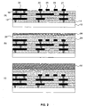
- FIG. 2 schematically depicts the various steps of a method of manufacturing an IC with a gas sensor, i.e. a sensor exposed to the environment of the IC, said method being outside the scope of the present invention, inwhich the gas sensor can be integrated using processing steps that are readily available in the manufacturing process of the IC.
- the manufacturing process preferably is a CMOS process.
- an IC may be provided comprising a substrate 10 onto which a metallization stack is formed.
- a metallization stack typically comprises a stack of patterned metal layers 12 electrically insulated from each other by electrically insulating, i.e. dielectric layers 14.
- Metal portions in different metallization layers 12 may be conductively coupled to each other by means of vias 16 extending through dielectric layers 14 separating such metal portions from each other.
- the substrate 10 may be any suitable substrate material, e.g. single crystal Si, SiGe, silicon on insulator and so on, and may carry a plurality of circuit elements such as transistors, diodes and so on.
- the metallization stack may be formed in any suitable manner, and may contain any suitable number of metal layers 12 and dielectric layers 14. It should be understood that three metal layers are shown by way of non-limiting example only.
- Each metal layer 12 and each dielectric layer 14 is depicted as a single layer in Fig. 2 for the sake of clarity only. It should be appreciated that such layers may consist of a number of stacked sub-layers, for instance in a submicron CMOS process, stacks of Ti, TiN, AlCu, TiN may be used to define a single metal layer in the metallization stack.
- Each of the dielectric layers 14 may also comprise more than a single layer.
- a dielectric layer may be a stack comprising FSG (fluorosilicate glass), SiO 2 and HDP oxide (High Density Plasma) any other suitable dielectric material combination.
- FSG fluorosilicate glass
- SiO 2 silicon dioxide
- HDP oxide High Density Plasma
- Other suitable materials may also be used.
- the vias 16 may be formed from more than a single material.
- a via 16 may be formed by a TiN liner and a W plug.
- Other semiconductor processes may use different materials, e.g. Cu for the metal layers 12 and vias 16.
- the upper metal layer of the metallization stack comprises a first electrode portion 20, a second electrode portion 21, a bond pad portion 22 and an optional heating element 23.
- the heating element 23 may be implemented as a meander line in the upper metal layer. Alternatively, the heating element 23 may be omitted.
- step (b) the metallization stack is covered by a passivation stack, which may comprise the deposition of a high density plasma oxide 24 followed by an oxide planarization step, e.g. a chemical mechanical polishing (CMP) step, after which a SiO 2 layer 26 and a Si 3 N 4 layer 28 may be deposited to any suitable thickness.
- CMP chemical mechanical polishing
- Other layer materials may also be contemplated for the passivation stack. It is known per se to the skilled person how to form such a passivation stack such that this will not be elaborated upon for reasons of brevity only.
- step (c) the method proceeds as shown in step (c), in which an aluminum layer 30 is deposited onto the passivation stack.
- This deposition may for instance be achieved using chemical vapor deposition (CVD) or plasma vapor deposition (PVD).
- the aluminum layer 30 has a thickness of one to several micrometers, e.g. 5 ⁇ m or more.
- step (d) the aluminum layer 30 is anodically oxidized to convert the aluminum layer 30 into an anodic aluminum oxide 32.
- This may for instance be achieved by immersing the wafer in a liquid electrolyte/acid bath and applying a voltage across the aluminum layer 30 and an electrode in the immersion bath. It is noted that the other components of the IC remain protected by the passivation stack.
- Anodically oxidized aluminum is a self-organized nanoporous material that contains a high density of cylindrical nanopores that align perpendicularly to the surface supporting the nanopores.
- This support may for instance be an unreacted portion of the aluminum layer 30, which may be located at the bottom of the oxidized portion as well as in between its pores.
- a dense aluminum oxide film is formed separating the pores from the aluminum support.
- the pore diameter may be tuned in a large range, i.e. from 5 to several hundreds of nanometers, with the corresponding pore density ranges from 10 12 -10 9 cm -1 .
- the pores increase the specific surface area of the material, thus providing a larger surface area for the gas to adhere to.
- the anodic aluminum oxide 32 may be functionalized to make the anodic aluminum oxide 32 sensitive to a particular type of gas, e.g. CO 2 .
- a particular type of gas e.g. CO 2
- This may for instance be achieved by deposition a metal oxide such as ZnO onto the anodic aluminum oxide 32, which preferably is performed in a highly conformal manner to ensure efficient penetration of the metal oxide into the pores of the anodic aluminum oxide 32.
- This may for instance be achieved by atomic layer deposition (ALD).
- the anodic aluminum oxide 32 is patterned into a sensing material portion on the passivation stack located above (i.e. opposite to) the heating element 23 in the upper metal layer, if present.
- This patterning may be achieved using patterning techniques that are well-known per se; for instance, a resist may be deposited, exposed through a lithographic mask and developed to cover only the part of the anodic aluminum oxide layer 32 to remain on the passivation stack, after which the exposed anodic aluminum oxide 32 is etched away stopping on the passivation stack, followed by the subsequent removal of the resist from the remaining portion of the anodic aluminum oxide 32.
- the passivation stack is opened by forming trenches 34 that at least expose the contacts 20, 21 and may also expose the bond pad 22. This is shown in step (f).
- This patterning may be achieved using patterning techniques that are well-known per se; for instance, a resist may be deposited, exposed through a lithographic mask and developed to expose only the parts of the passivation stack to be opened, after which the exposed passivation stack is etched away stopping on the upper metal layer of the metallization stack, followed by the subsequent removal of the resist from the remaining portions of the passivation stack.
- step (g) a metal layer 36 defining the sensor contacts is deposited in any suitable manner, e.g. by PVD or CVD, after which the metal layer 36 is patterned as shown in step (h) to define the first conductive portion 38 that connects one side of the anodized aluminum oxide portion 32 to the first electrode contact 20 and a second conductive portion 40 that connects an opposite side of the anodized aluminum oxide portion 32 to the second electrode contact 21 such that the anodized aluminum oxide portion 32 laterally extends between the first conductive portion 38 and the second conductive portion 40.
- the patterning of the metal layer 36 may be achieved in any suitable manner, e.g.
- step (h) the metal 36 has been removed from the bond pad 22 it should be understood that it is equally feasible to maintain a metal portion over the bond pad 22.
- the IC may subsequently be finalized, e.g. packaged, in any suitable manner.
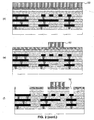
- FIG. 3 depicts an alternative embodiment of the method of FIG. 2 outside the scope of the present invention, which proceeds from the intermediate IC structure obtained after step (e) of FIG. 2 .
- the anodized aluminum oxide portion 32 may still comprise an aluminum support layer, which for instance can occur when the aluminum layer 30 is not fully oxidized. This is shown in FIG. 3(a) .
- the aluminum support layer 30 may form a low-resistance conductive path between the first conductive portion 38 and the second conductive portion 40, which bypasses (short-circuits) the functionalized anodized aluminum oxide portion 32, thus disabling the gas sensor, i.e. rendering the gas sensor non-functional.
- an additional processing step may be added to the method of FIG. 2 .
- This additional processing step takes place before the passivation stack is opened and is shown in FIG. 3(b) .
- a selective aluminum etch that does not attack Al 2 O 3 is performed, which creates an underetch or recess 42 underneath the anodic aluminum oxide portion 32 such that upon the formation of the first conductive portion 38 and the second conductive portion 40 as explained in more detail with the aid of FIG. 2 a finalized gas sensor is obtained as shown in FIG. 3(c) , in which the first conductive portion 38 and the second conductive portion 40 are electrically insulated from the aluminum support layer 30 by the recess or void 42.
- FIG. 4 an alternative embodiment of electrically insulating the first conductive portion 38 and the second conductive portion 40 from the aluminum support layer 30 is shown in FIG. 4 , which takes the intermediate IC structure as shown in FIG. 2(e) as starting point.
- a layer 50 of an electrically insulating material such as an oxide, nitride, low-k dielectric and so on, is deposited over the resulting structure as shown in step (a), followed by the patterning of the electrically insulating material into electrically insulating side wall spacers 52 as shown in step (b). This may for instance be achieved by a spacer etch, which is well-known per se.
- the gas sensor may be completed as shown in FIG. 2 , i.e. by opening the passivation layer and forming the first conductive portion 38 and the second conductive portion 40, which are electrically insulated from the aluminum support layer 30 by the sidewall spacers 52.
- the resultant structure is shown in FIG. 4(c) .
- the sidewall spacers 52 may have any suitable shape, and may for instance have a portion that extends over the upper surface of the anodic aluminum oxide portion 32 to further improve the electrical insulation of the first conductive portion 38 and the second conductive portion 40 from the aluminum support layer 30.
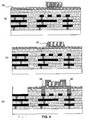
- FIG. 3 and FIG. 4 have in common that electrical insulation means are formed between the aluminum support layer 30 and the first conductive portion 38 and the second conductive portion 40 respectively.
- contact portions 60 and 62 are formed on opposite edge portions of the upper surface of the anodic aluminum oxide portion 32, which may be achieved by a metal deposition step, e.g. a CVD or PVD deposition step, followed by the formation of a patterned resist and metal etch from the areas exposed by the patterned resist and subsequent resist removal.
- the passivation stack may be opened as shown in FIG.
- first conductive portion 38 and the second conductive portion 40 in the form of bond wires from the first contact portion 60 to the first metal portion 20 and from the second contact portion 62 to the second metal portion 21 respectively.
- bond wires are not in physical contact with the side walls of the aluminum support layer 30 and the anodic aluminum oxide portion 32, a short-circuit of the gas sensor is avoided.
- the porous material used for the gas sensor of the present invention is not limited to anodic aluminum oxide. Any suitable porous material may be used, although it is preferable for cost reasons to use materials that are already used in the IC manufacturing process.
- Step (a) and step (b) are completely analogous with step (a) and (b) as shown in FIG. 2 and will therefore not be described again for the sake of brevity.
- a substrate material 70 e.g. silicon, silicon oxide or silicon nitride, is deposited over the passivation stack of the lC. This may for instance be achieved using CVD or PVD deposition techniques. Alternatively, the substrate material 70 may be epitaxially grown on the passivation stack. The substrate material 70 is subsequently patterned into a substrate portion 72, which is located over the heating element 23 if present. This is shown in step (d).
- a substrate material 70 e.g. silicon, silicon oxide or silicon nitride
- the substrate 70 is typically patterned such that upon the removal of the substrate 70 from the areas other than the area of the substrate portion 72, the substrate portion 72 is made porous by etching micro-pores into the substrate portion 72. This can for instance readily be achieved by defining a mask portion over the substrate portion 72 to have openings of nanometer dimensions. It is noted that this is routinely feasible in submicron manufacturing processes such as a submicron CMOS process in which feature sizes of only a few hundred nanometers can be routinely achieved, e.g. when etching via trenches through dielectric layers.
- this porous portion may be functionalized, e.g. by a high-conformal deposition of a metal oxide such as ZnO for a CO 2 sensor as previously explained.
- a metal oxide such as ZnO for a CO 2 sensor
- Other suitable functionalization materials will be apparent to the skilled person.
- the resulting functionalized porous substrate portion 74 is shown in step (e). In an embodiment outside the scope of the present invention, the method may now proceed analogously to what has already been explained in detail in the detailed description of FIG. 2 , i.e.
- step (f) depositing a metal layer 36 over the resultant structure as shown in step (g) and patterning the metal layer 36 to form the first conductive portion 38 and the second conductive portion 40 connecting the gas-sensitive substrate portion 74 to the first contact portion 20 and the second contact portion 21 respectively.
- the aluminum layer 30 is oxidized prior to patterning. It is equally feasible to first pattern the aluminum layer 30 into the sensor portion and subsequently oxidize and functionalize this portion.
- FIG. 3-5 may be combined resulting in embodiments outside the scope of the present invention.
- bond wires 60 and 62 may be used in combination with side wall spacers 52 or the recess 42 to further reduce the risk of the aforementioned short-circuit occurring.
- the substrate layer 70 has been patterned prior to its functionalization. It is of course equally feasible to first make the substrate layer 70 porous, subsequently functionalize the porous layer after which the functionalized porous layer may be patterned into functionalized porous substrate portion 74. Alternatively, the substrate layer may first be made porous, subsequently patterned and functionalized following patterning.
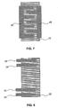
- the arrangement of the conductive portions 38 and 40 on the gas sensitive portion on the passivation stack may be possible to the arrangement of the conductive portions 38 and 40 on the gas sensitive portion on the passivation stack.
- an arrangement with interdigitated contact portions 38 and 40 on top of the gas sensitive portion may be contemplated such that the interdigitated contact portions 38 and 40 are electrically insulated from each other by a meandering portion of the gas sensitive portion 32 or 74.
- An example embodiment with a gas sensitive portion 32 is shown in FIG. 7 .
- Other arrangements that are known per se will be readily available to the skilled person.
- the gas sensitive portion may be contacted by more than two electrodes.
- the lC may further comprise an additional pair of contact portions 38' and 40' forming an outer electrode pair.
- the outer electrode pair may be used to force a current through the gas sensitive portion such as a gas sensitive portion 32 as shown in FIG. 8 , with the inner electrode pair being arranged to measure the voltage drop across the gas sensitive portion.
- the IC of the present invention may be integrated in any suitable electronic device, e.g. a mobile communication device such as a mobile phone, personal digital assistant and so on, or may be used as a tag for an article for monitoring purposes, in which case the lC may be extended with RF functionality, e.g. an RF transceiver communicatively coupled to the sensor(s) of the IC.
- a mobile communication device such as a mobile phone, personal digital assistant and so on
- RF functionality e.g. an RF transceiver communicatively coupled to the sensor(s) of the IC.
Landscapes
- Chemical & Material Sciences (AREA)
- Health & Medical Sciences (AREA)
- Life Sciences & Earth Sciences (AREA)
- Immunology (AREA)
- Analytical Chemistry (AREA)
- Biochemistry (AREA)
- General Health & Medical Sciences (AREA)
- General Physics & Mathematics (AREA)
- Physics & Mathematics (AREA)
- Pathology (AREA)
- Chemical Kinetics & Catalysis (AREA)
- Electrochemistry (AREA)
- Engineering & Computer Science (AREA)
- Food Science & Technology (AREA)
- Medicinal Chemistry (AREA)
- Combustion & Propulsion (AREA)
- Investigating Or Analyzing Materials By The Use Of Electric Means (AREA)
- Investigating Or Analyzing Materials By The Use Of Fluid Adsorption Or Reactions (AREA)
- Pressure Sensors (AREA)
Description
- The present invention relates to an integrated circuit (IC) comprising a substrate carrying a plurality of circuit elements; a metallization stack interconnecting said circuit elements, said metallization stack comprising a patterned upper metallization layer comprising a first metal portion; a passivation stack covering the metallization stack; and a sensor.
- The present invention further relates to a method of manufacturing such an IC.
- Nowadays, integrated circuits (ICs) may comprise a plethora of sensors, such as gas sensors, relative humidity (RH) sensors, specific analyte detection sensors, and so on. Such sensors may be included in the IC design for a number of reasons.
- For instance, a gas sensor may be included in an IC to detect a change in the ambient conditions of a product tagged with the chip such that product quality control can be achieved by monitoring the sensor readings of the chip. This can for instance be used to accurately predict the remaining shelf life of the product, e.g. perishable food stuff. The gas sensor may for instance be adapted to determine changes in the CO2 content of the ambient atmosphere. Alternatively, the gas sensor may be used to detect changes in the gas composition of larger environment such as buildings or may be used in medical application domains, e.g. in breathing apparatuses.
- It is particularly relevant to mass market applications such as RF tags for product monitoring that the gas sensor functionality can be added to the IC with limited additional cost, as there is a large price pressure on such ICs; i.e. they have to be produced cheaply in order to be commercially attractive.
- It is clear that there is a desire for the integration of a variety of sensors such as gas sensor onto an IC in a cost-effective manner.
-
WO 2005/095936 describes an integrated sensor device and method of manufacturing the device. The device includes: MOS circuits in a semiconductor substrate, interconnect levels with interconnect conductors and insulating dielectric, said levels being over the substrate and interconnecting the MOS circuits, the interconnect levels incorporating a sensor having electrodes embedded in the interconnect dielectric, and the MOS circuits including a processor for processing signals from the sensor electrodes. -
US 2002/118027 describes a type of nanostructured ceramic platform for gas sensors and sensor arrays. These sensors comprise micromachined anodic aluminum oxide films. - The present invention seeks to provide an IC comprising a gas sensor that can be readily provided using standard IC manufacturing methods.
- The present invention further seeks to provide a method of manufacturing such an IC.
- According to the present invention, there is provided an integrated circuit according to
claim 1. - The present invention is based on the insight that gas-sensitive materials may be deposited on top of the passivation stack and connected to contacts in the metallization stack using standard processing techniques. In an embodiment, the sensing material comprises a porous layer comprising at least one metal oxide. Such a porous layer may for instance be a porous substrate layer functionalized with said at least one metal oxide, which can be formed using standard processing steps; the pores may be formed by standard etching techniques and the metal oxide can be formed using standard deposition techniques such as ALD, CVD, PE-CVD and so on. Alternatively, the porous substrate layer comprises anodic aluminium oxide, which may be formed by an aluminum deposition followed by an anodic oxidation step, thus forming a self-aligned nanoporous material as is known per se.
- The integrated circuit may further comprise a heating element in an metallization layer of the metallization stack, said heating element being located opposite the sensing material portion. This has the advantage that the operating temperature of the gas sensor may be controlled, thus facilitating the detection of gases that can only be detected at elevated temperatures and the acceleration of the reaction and recovery time of the gas sensor. The metallization layer housing the heating element preferably is the upper metallization layer.
- According to the present invention, there is provided a method of manufacturing an integrated circuit according to claim 7.
- Such a method facilitates the formation of a gas sensor in a standard manufacturing process, in particular a standard CMOS process.
- The step of forming a gas sensor including a sensing material portion on the passivation stack may comprise forming a substrate portion on the passivation stack; etching pores into said substrate portion; and at least partially filling said pores with at least one metal oxide. This has the advantage that the risk of the occurrence of a short circuit due to the incomplete oxidation of a metal portion can be largely avoided.
- Alternatively, the step of forming a gas sensor including a sensing material portion on the passivation stack comprises forming an aluminum layer portion on the passivation stack; and anodically oxidizing said aluminum layer portion. This has the advantage that the sensing material portion may be formed in a simple two-step process, thus yielding a particularly cost-effective IC.
- Embodiments of the invention are described in more detail and by way of non-limiting examples with reference to the accompanying drawings, wherein:
-
FIG. 1 schematically depicts an example operating principle of a gas sensor; -
FIG. 2 schematically depicts a method to manufacture an IC with a gas sensor outside the scope of the present invention; -
FIG. 3 schematically depicts a method to manufacture an IC with a gas sensor outside the scope of the present invention; -
FIG. 4 schematically depicts a method to manufacture an IC with a sensor in accordance with the present invention; -
FIG. 5 schematically depicts a method to manufacture an IC with a sensor outside the scope of the present invention; -
FIG. 6 schematically depicts a method to manufacture an IC with a sensor outside the scope of the present invention; -
FIG. 7 schematically depicts a top view of an IC comprising a gas sensor according to yet another embodiment of the present invention; and -
FIG. 8 schematically depicts a top view of an IC comprising a gas sensor according to yet another embodiment of the present invention. - It should be understood that the Figures are merely schematic and are not drawn to scale. It should also be understood that the same reference numerals are used throughout the Figures to indicate the same or similar parts.
-
FIG. 1 schematically depicts an operating principle of a gas sensor. A gas-sensitive material portion 32 is placed in a conductive path between afirst contact 20 and asecond contact 21. The gas-sensitive material portion 32 acts as a variable resistor with its resistance dependent on the level of exposure of the gas to be monitored. The adsorption of gas to the surface of the gas-sensitive material portion 32 changes the electrical resistance of the material, either by the occurrence of an oxidation reaction in which electrons are transferred from the gas-sensitive material portion 32 to the gas or a reduction reaction in which electrons are transferred from the gas to the gas-sensitive material portion 32. As the reaction rate scales with the concentration of the gas, the measured resistance can be translated into a gas concentration. The gas-sensitive material portion 32 is typically chosen to have a high specific surface area such that relatively large volumes of gas can adsorb to the gas-sensitive material portion 32, thus improving signal-to-noise characteristics of the gas sensor. -
FIG. 2 schematically depicts the various steps of a method of manufacturing an IC with a gas sensor, i.e. a sensor exposed to the environment of the IC, said method being outside the scope of the present invention, inwhich the gas sensor can be integrated using processing steps that are readily available in the manufacturing process of the IC. The manufacturing process preferably is a CMOS process. - As shown in step (a), an IC may be provided comprising a
substrate 10 onto which a metallization stack is formed. Such a metallization stack typically comprises a stack of patternedmetal layers 12 electrically insulated from each other by electrically insulating, i.e.dielectric layers 14. Metal portions indifferent metallization layers 12 may be conductively coupled to each other by means ofvias 16 extending throughdielectric layers 14 separating such metal portions from each other. Thesubstrate 10 may be any suitable substrate material, e.g. single crystal Si, SiGe, silicon on insulator and so on, and may carry a plurality of circuit elements such as transistors, diodes and so on. - Equally, the metallization stack may be formed in any suitable manner, and may contain any suitable number of
metal layers 12 anddielectric layers 14. It should be understood that three metal layers are shown by way of non-limiting example only. - Each
metal layer 12 and eachdielectric layer 14 is depicted as a single layer inFig. 2 for the sake of clarity only. It should be appreciated that such layers may consist of a number of stacked sub-layers, for instance in a submicron CMOS process, stacks of Ti, TiN, AlCu, TiN may be used to define a single metal layer in the metallization stack. - Each of the
dielectric layers 14 may also comprise more than a single layer. For instance, such a dielectric layer may be a stack comprising FSG (fluorosilicate glass), SiO2 and HDP oxide (High Density Plasma) any other suitable dielectric material combination. Other suitable materials may also be used. - Similarly, it will be apparent that the
vias 16 may be formed from more than a single material. For instance, in a 140 nm CMOS technology, avia 16 may be formed by a TiN liner and a W plug. Other semiconductor processes may use different materials, e.g. Cu for the metal layers 12 andvias 16. - In
FIG. 2 , the upper metal layer of the metallization stack comprises afirst electrode portion 20, asecond electrode portion 21, abond pad portion 22 and anoptional heating element 23. Theheating element 23 may be implemented as a meander line in the upper metal layer. Alternatively, theheating element 23 may be omitted. - In step (b), the metallization stack is covered by a passivation stack, which may comprise the deposition of a high
density plasma oxide 24 followed by an oxide planarization step, e.g. a chemical mechanical polishing (CMP) step, after which a SiO2 layer 26 and a Si3N4 layer 28 may be deposited to any suitable thickness. Other layer materials may also be contemplated for the passivation stack. It is known per se to the skilled person how to form such a passivation stack such that this will not be elaborated upon for reasons of brevity only. - The method proceeds as shown in step (c), in which an
aluminum layer 30 is deposited onto the passivation stack. This deposition may for instance be achieved using chemical vapor deposition (CVD) or plasma vapor deposition (PVD). Preferably, thealuminum layer 30 has a thickness of one to several micrometers, e.g. 5 µm or more. - In step (d), the
aluminum layer 30 is anodically oxidized to convert thealuminum layer 30 into ananodic aluminum oxide 32. This may for instance be achieved by immersing the wafer in a liquid electrolyte/acid bath and applying a voltage across thealuminum layer 30 and an electrode in the immersion bath. It is noted that the other components of the IC remain protected by the passivation stack. - Anodically oxidized aluminum is a self-organized nanoporous material that contains a high density of cylindrical nanopores that align perpendicularly to the surface supporting the nanopores. This support may for instance be an unreacted portion of the
aluminum layer 30, which may be located at the bottom of the oxidized portion as well as in between its pores. Typically, a dense aluminum oxide film is formed separating the pores from the aluminum support. By controlling the anodizing reaction conditions, the pore diameter may be tuned in a large range, i.e. from 5 to several hundreds of nanometers, with the corresponding pore density ranges from 1012-109 cm-1. The pores increase the specific surface area of the material, thus providing a larger surface area for the gas to adhere to. - Next, the
anodic aluminum oxide 32 may be functionalized to make theanodic aluminum oxide 32 sensitive to a particular type of gas, e.g. CO2. This may for instance be achieved by deposition a metal oxide such as ZnO onto theanodic aluminum oxide 32, which preferably is performed in a highly conformal manner to ensure efficient penetration of the metal oxide into the pores of theanodic aluminum oxide 32. This may for instance be achieved by atomic layer deposition (ALD). - As shown in step (e), the
anodic aluminum oxide 32 is patterned into a sensing material portion on the passivation stack located above (i.e. opposite to) theheating element 23 in the upper metal layer, if present. This patterning may be achieved using patterning techniques that are well-known per se; for instance, a resist may be deposited, exposed through a lithographic mask and developed to cover only the part of the anodicaluminum oxide layer 32 to remain on the passivation stack, after which the exposedanodic aluminum oxide 32 is etched away stopping on the passivation stack, followed by the subsequent removal of the resist from the remaining portion of theanodic aluminum oxide 32. - Next, the passivation stack is opened by forming
trenches 34 that at least expose thecontacts bond pad 22. This is shown in step (f). This patterning may be achieved using patterning techniques that are well-known per se; for instance, a resist may be deposited, exposed through a lithographic mask and developed to expose only the parts of the passivation stack to be opened, after which the exposed passivation stack is etched away stopping on the upper metal layer of the metallization stack, followed by the subsequent removal of the resist from the remaining portions of the passivation stack. - The method then proceeds as shown in step (g), in which a
metal layer 36 defining the sensor contacts is deposited in any suitable manner, e.g. by PVD or CVD, after which themetal layer 36 is patterned as shown in step (h) to define the firstconductive portion 38 that connects one side of the anodizedaluminum oxide portion 32 to thefirst electrode contact 20 and a secondconductive portion 40 that connects an opposite side of the anodizedaluminum oxide portion 32 to thesecond electrode contact 21 such that the anodizedaluminum oxide portion 32 laterally extends between the firstconductive portion 38 and the secondconductive portion 40. As before, the patterning of themetal layer 36 may be achieved in any suitable manner, e.g. by resist deposition, lithographic exposure and development, subsequent metal layer etch and resist removal. Although in step (h) themetal 36 has been removed from thebond pad 22 it should be understood that it is equally feasible to maintain a metal portion over thebond pad 22. The IC may subsequently be finalized, e.g. packaged, in any suitable manner. -
FIG. 3 depicts an alternative embodiment of the method ofFIG. 2 outside the scope of the present invention, which proceeds from the intermediate IC structure obtained after step (e) ofFIG. 2 . As previously explained, the anodizedaluminum oxide portion 32 may still comprise an aluminum support layer, which for instance can occur when thealuminum layer 30 is not fully oxidized. This is shown inFIG. 3(a) . Upon forming the firstconductive portion 38 and the secondconductive portion 40 as shown inFIG. 2(h) , thealuminum support layer 30 may form a low-resistance conductive path between the firstconductive portion 38 and the secondconductive portion 40, which bypasses (short-circuits) the functionalized anodizedaluminum oxide portion 32, thus disabling the gas sensor, i.e. rendering the gas sensor non-functional. - In order to prevent the occurrence of such a short-circuit an additional processing step may be added to the method of
FIG. 2 . This additional processing step takes place before the passivation stack is opened and is shown inFIG. 3(b) . A selective aluminum etch that does not attack Al2O3 is performed, which creates an underetch orrecess 42 underneath the anodicaluminum oxide portion 32 such that upon the formation of the firstconductive portion 38 and the secondconductive portion 40 as explained in more detail with the aid ofFIG. 2 a finalized gas sensor is obtained as shown inFIG. 3(c) , in which the firstconductive portion 38 and the secondconductive portion 40 are electrically insulated from thealuminum support layer 30 by the recess or void 42. - According to the present invention, an alternative embodiment of electrically insulating the first
conductive portion 38 and the secondconductive portion 40 from thealuminum support layer 30 is shown inFIG. 4 , which takes the intermediate IC structure as shown inFIG. 2(e) as starting point. Alayer 50 of an electrically insulating material such as an oxide, nitride, low-k dielectric and so on, is deposited over the resulting structure as shown in step (a), followed by the patterning of the electrically insulating material into electrically insulatingside wall spacers 52 as shown in step (b). This may for instance be achieved by a spacer etch, which is well-known per se. - The gas sensor may be completed as shown in
FIG. 2 , i.e. by opening the passivation layer and forming the firstconductive portion 38 and the secondconductive portion 40, which are electrically insulated from thealuminum support layer 30 by thesidewall spacers 52. The resultant structure is shown inFIG. 4(c) . It is pointed out that thesidewall spacers 52 may have any suitable shape, and may for instance have a portion that extends over the upper surface of the anodicaluminum oxide portion 32 to further improve the electrical insulation of the firstconductive portion 38 and the secondconductive portion 40 from thealuminum support layer 30. - It is noted that
FIG. 3 andFIG. 4 have in common that electrical insulation means are formed between thealuminum support layer 30 and the firstconductive portion 38 and the secondconductive portion 40 respectively. However, in an alternative embodiment shown inFIG. 5 outside the scope of the present invention,contact portions aluminum oxide portion 32, which may be achieved by a metal deposition step, e.g. a CVD or PVD deposition step, followed by the formation of a patterned resist and metal etch from the areas exposed by the patterned resist and subsequent resist removal. The passivation stack may be opened as shown inFIG. 2(f) , followed by the formation of the firstconductive portion 38 and the secondconductive portion 40 in the form of bond wires from thefirst contact portion 60 to thefirst metal portion 20 and from thesecond contact portion 62 to thesecond metal portion 21 respectively. As the bond wires are not in physical contact with the side walls of thealuminum support layer 30 and the anodicaluminum oxide portion 32, a short-circuit of the gas sensor is avoided. - The porous material used for the gas sensor of the present invention is not limited to anodic aluminum oxide. Any suitable porous material may be used, although it is preferable for cost reasons to use materials that are already used in the IC manufacturing process.
- An embodiment of the present invention using such an alternative embodiment is shown in
FIG. 6 . Step (a) and step (b) are completely analogous with step (a) and (b) as shown inFIG. 2 and will therefore not be described again for the sake of brevity. - In step (c), a
substrate material 70, e.g. silicon, silicon oxide or silicon nitride, is deposited over the passivation stack of the lC. This may for instance be achieved using CVD or PVD deposition techniques. Alternatively, thesubstrate material 70 may be epitaxially grown on the passivation stack. Thesubstrate material 70 is subsequently patterned into asubstrate portion 72, which is located over theheating element 23 if present. This is shown in step (d). - The
substrate 70 is typically patterned such that upon the removal of thesubstrate 70 from the areas other than the area of thesubstrate portion 72, thesubstrate portion 72 is made porous by etching micro-pores into thesubstrate portion 72. This can for instance readily be achieved by defining a mask portion over thesubstrate portion 72 to have openings of nanometer dimensions. It is noted that this is routinely feasible in submicron manufacturing processes such as a submicron CMOS process in which feature sizes of only a few hundred nanometers can be routinely achieved, e.g. when etching via trenches through dielectric layers. - Upon providing the
porous substrate portion 72, this porous portion may be functionalized, e.g. by a high-conformal deposition of a metal oxide such as ZnO for a CO2 sensor as previously explained. Other suitable functionalization materials will be apparent to the skilled person. The resulting functionalizedporous substrate portion 74 is shown in step (e). In an embodiment outside the scope of the present invention, the method may now proceed analogously to what has already been explained in detail in the detailed description ofFIG. 2 , i.e. by forming thetrenches 34 through the passivation stack as shown in step (f), depositing ametal layer 36 over the resultant structure as shown in step (g) and patterning themetal layer 36 to form the firstconductive portion 38 and the secondconductive portion 40 connecting the gas-sensitive substrate portion 74 to thefirst contact portion 20 and thesecond contact portion 21 respectively. - It is pointed out that variations to the shown manufacturing processes will be apparent to the skilled person, such that these variations are intended to fall under the scope of the present invention.
- For instance, as shown in
FIG. 2-5 , thealuminum layer 30 is oxidized prior to patterning. It is equally feasible to first pattern thealuminum layer 30 into the sensor portion and subsequently oxidize and functionalize this portion. - The embodiments of
FIG. 3-5 may be combined resulting in embodiments outside the scope of the present invention. For instance,bond wires side wall spacers 52 or therecess 42 to further reduce the risk of the aforementioned short-circuit occurring. - Similarly, in
FIG. 6 , thesubstrate layer 70 has been patterned prior to its functionalization. It is of course equally feasible to first make thesubstrate layer 70 porous, subsequently functionalize the porous layer after which the functionalized porous layer may be patterned into functionalizedporous substrate portion 74. Alternatively, the substrate layer may first be made porous, subsequently patterned and functionalized following patterning. - Finally, it should be understood that many variants may be possible to the arrangement of the
conductive portions interdigitated contact portions contact portions sensitive portion sensitive portion 32 is shown inFIG. 7 . Other arrangements that are known per se will be readily available to the skilled person. - It should furthermore be understood that the gas sensitive portion may be contacted by more than two electrodes. For instance, as shown in
FIG. 8 , in addition to thecontact portions sensitive portion 32 as shown inFIG. 8 , with the inner electrode pair being arranged to measure the voltage drop across the gas sensitive portion. Again, such an electrode arrangement is known per se and alternative arrangements will be readily available to the skilled person. - The IC of the present invention may be integrated in any suitable electronic device, e.g. a mobile communication device such as a mobile phone, personal digital assistant and so on, or may be used as a tag for an article for monitoring purposes, in which case the lC may be extended with RF functionality, e.g. an RF transceiver communicatively coupled to the sensor(s) of the IC.
Claims (9)
- An integrated circuit comprising:a substrate (10) carrying a plurality of circuit elements;a metallization stack (12, 14, 16) interconnecting said circuit elements, said metallization stack comprising a patterned upper metallization layer comprising a first metal portion (20) and a second metal portion (21);a passivation stack (24, 26, 28) covering the metallization stack;a gas sensor including a sensing material portion (32, 74) on a support layer (30) on the passivation stack;a first conductive portion (38) extending through the passivation stack connecting a first region of the sensing material portion (32, 74) to the first metal portion (20);a second conductive portion (40) extending through the passivation stack connecting a second region of the sensing material portion (32, 74) to the second metal portion (21); andelectrically insulating sidewall spacers (52) adjacent the sensing material portion (32, 74), each for electrically insulating a respective conductive portion (38, 40) extending through the passivation stack from the support layer (30).
- The integrated circuit of claim 1, wherein the sensing material comprises a porous layer comprising at least one metal oxide.
- The integrated circuit of claim 2, wherein the porous layer (74) is a substrate layer functionalized with said at least one metal oxide.
- The integrated circuit of claim 3, wherein the at least one metal oxide is selected from ZnO and Al2O3.
- The integrated circuit of claim 2, wherein the porous layer (32) comprises anodic aluminium oxide.
- The integrated circuit of any preceding claim, further comprising a heating element (23) in a metallization layer of the metallization stack, said heating element being located opposite the sensing material portion (32, 74).
- A method of manufacturing an integrated circuit, comprising:providing a substrate (10) carrying a plurality of circuit elements;forming a metallization stack (12, 14, 16) interconnecting said circuit elements, said metallization stack comprising a patterned upper metallization layer comprising a first metal portion (20) and a second metal portion (21);forming a passivation stack (24, 26, 28) covering the metallization stack;forming a gas sensor including a sensing material portion (32, 74) on a support layer (30) on the passivation stack;forming electrically insulating sidewall spacers (52) adjacent the sensing material portion (32, 74);opening the passivation stack to expose the first metal portion (20) and the second metal portion (21); andforming a first conductive portion (38) between a first region of the sensing material portion (32, 74) and the first metal portion (20) and a second conductive portion (40) between a second region of the sensing material portion (32, 74) and the second metal portion (21),wherein the electrically insulating spacers (52) each electrically insulate a respective conductive portion (38,40) extending through the passivation stack from the support layer (30).
- The method of claim 7, wherein the step of forming a gas sensor including a sensing material portion (74) on the passivation stack comprises:forming a substrate portion (72) on the passivation stack (24, 26, 28);etching pores into said substrate portion; andat least partially filling said pores with at least one metal oxide.
- The method of claim 7, wherein the step of forming a gas sensor including a sensing material portion (32) on the passivation stack comprises:forming an aluminum layer portion (30) on the passivation stack (24, 26, 28); andanodically oxidizing said aluminum layer portion.
Priority Applications (5)
| Application Number | Priority Date | Filing Date | Title |
|---|---|---|---|
| EP11176484.1A EP2554980B1 (en) | 2011-08-03 | 2011-08-03 | Integrated circuit with sensor and method of manufacturing such an integrated circuit |
| EP11191420.6A EP2554981B1 (en) | 2011-08-03 | 2011-11-30 | Integrated circuit with a gas sensor and method of manufacturing such an integrated circuit |
| US13/556,926 US10197520B2 (en) | 2011-08-03 | 2012-07-24 | Integrated circuit with sensor and method of manufacturing such an integrated circuit |
| US13/556,676 US8853798B2 (en) | 2011-08-03 | 2012-07-24 | Integrated circuit with sensor and method of manufacturing such an integrated circuit |
| CN201210272151.3A CN102915993B (en) | 2011-08-03 | 2012-08-01 | There is the integrated circuit of transducer and manufacture the method for this integrated circuit |
Applications Claiming Priority (1)
| Application Number | Priority Date | Filing Date | Title |
|---|---|---|---|
| EP11176484.1A EP2554980B1 (en) | 2011-08-03 | 2011-08-03 | Integrated circuit with sensor and method of manufacturing such an integrated circuit |
Publications (2)
| Publication Number | Publication Date |
|---|---|
| EP2554980A1 EP2554980A1 (en) | 2013-02-06 |
| EP2554980B1 true EP2554980B1 (en) | 2014-06-25 |
Family
ID=45002845
Family Applications (2)
| Application Number | Title | Priority Date | Filing Date |
|---|---|---|---|
| EP11176484.1A Active EP2554980B1 (en) | 2011-08-03 | 2011-08-03 | Integrated circuit with sensor and method of manufacturing such an integrated circuit |
| EP11191420.6A Active EP2554981B1 (en) | 2011-08-03 | 2011-11-30 | Integrated circuit with a gas sensor and method of manufacturing such an integrated circuit |
Family Applications After (1)
| Application Number | Title | Priority Date | Filing Date |
|---|---|---|---|
| EP11191420.6A Active EP2554981B1 (en) | 2011-08-03 | 2011-11-30 | Integrated circuit with a gas sensor and method of manufacturing such an integrated circuit |
Country Status (3)
| Country | Link |
|---|---|
| US (2) | US8853798B2 (en) |
| EP (2) | EP2554980B1 (en) |
| CN (1) | CN102915993B (en) |
Families Citing this family (14)
| Publication number | Priority date | Publication date | Assignee | Title |
|---|---|---|---|---|
| EP2554980B1 (en) | 2011-08-03 | 2014-06-25 | Nxp B.V. | Integrated circuit with sensor and method of manufacturing such an integrated circuit |
| EP2559996B1 (en) | 2011-08-16 | 2017-11-22 | Nxp B.V. | Gas sensor |
| EP2645091B1 (en) | 2012-03-30 | 2018-10-17 | ams international AG | Integrated circuit comprising a gas sensor |
| EP2793018A1 (en) * | 2013-04-19 | 2014-10-22 | Nxp B.V. | Thermal conductivity based gas sensor |
| WO2015066289A1 (en) * | 2013-10-30 | 2015-05-07 | Robert Bosch Gmbh | Metal oxide semiconductor sensor and method of forming a metal oxide semiconductor sensor using atomic layer deposition |
| WO2015071337A1 (en) * | 2013-11-12 | 2015-05-21 | Lfoundry S.R.L. | Integrated gas sensor and related manufacturing process |
| EP2905611B1 (en) | 2014-02-06 | 2018-01-17 | ams AG | Method of producing a semiconductor device with protruding contacts |
| US9453807B2 (en) | 2014-04-08 | 2016-09-27 | Ams International Ag | Thermal conductivity gas sensor with amplification material |
| WO2016088099A1 (en) * | 2014-12-05 | 2016-06-09 | Lfoundry S.R.L. | Cmos process for manufacturing an integrated gas sensor and corresponding cmos integrated gas sensor |
| CN106816439A (en) * | 2015-01-29 | 2017-06-09 | 江西师范大学 | The material of gas sensing layer is Ga2O3CMOS gas sensors |
| EP3062097A1 (en) * | 2015-02-27 | 2016-08-31 | EM Microelectronic-Marin SA | Moisture sensor with thermal module |
| US10429330B2 (en) * | 2016-07-18 | 2019-10-01 | Stmicroelectronics Pte Ltd | Gas analyzer that detects gases, humidity, and temperature |
| US10557812B2 (en) | 2016-12-01 | 2020-02-11 | Stmicroelectronics Pte Ltd | Gas sensors |
| WO2018200920A1 (en) | 2017-04-28 | 2018-11-01 | Corning Incorporated | Glass electrochemical sensor with wafer level stacking and through glass via (tgv) interconnects |
Family Cites Families (29)
| Publication number | Priority date | Publication date | Assignee | Title |
|---|---|---|---|---|
| US4215564A (en) | 1979-02-06 | 1980-08-05 | Gow-Mac Instrument Co. | Miniaturized thermal conductivity detector |
| JP3114139B2 (en) | 1995-01-24 | 2000-12-04 | 株式会社山武 | Thermal conductivity meter |
| GB2321336B (en) * | 1997-01-15 | 2001-07-25 | Univ Warwick | Gas-sensing semiconductor devices |
| US6705152B2 (en) * | 2000-10-24 | 2004-03-16 | Nanoproducts Corporation | Nanostructured ceramic platform for micromachined devices and device arrays |
| JP3610293B2 (en) * | 1999-09-22 | 2005-01-12 | キヤノン株式会社 | Structure having pores and device using the structure having pores |
| JP4501320B2 (en) * | 2001-07-16 | 2010-07-14 | 株式会社デンソー | Capacitive humidity sensor |
| US7296458B2 (en) * | 2002-10-17 | 2007-11-20 | Advanced Technology Materials, Inc | Nickel-coated free-standing silicon carbide structure for sensing fluoro or halogen species in semiconductor processing systems, and processes of making and using same |
| KR100476694B1 (en) * | 2002-11-07 | 2005-03-17 | 삼성전자주식회사 | structure of a Fuse for a semiconductor device and method of manufacturing the same |
| AU2003292630A1 (en) * | 2002-12-27 | 2004-07-29 | Matsushita Electric Industrial Co., Ltd. | Electronic device and method of manufacturing the same |
| US7003418B2 (en) * | 2003-08-28 | 2006-02-21 | Honeywell International Inc. | Methods and systems for temperature compensation of physical property sensors |
| US7053425B2 (en) * | 2003-11-12 | 2006-05-30 | General Electric Company | Gas sensor device |
| US7087451B2 (en) * | 2004-03-24 | 2006-08-08 | Intel Corporation | Microfabricated hot wire vacuum sensor |
| JP2005294308A (en) * | 2004-03-31 | 2005-10-20 | Fujitsu Ltd | Electronic element containing ferroelectric film and its manufacturing method |
| CN1961209A (en) * | 2004-04-02 | 2007-05-09 | 蒂莫西·卡明斯 | Integrated electronic sensor |
| US7269458B2 (en) * | 2004-08-09 | 2007-09-11 | Cardiac Pacemakers, Inc. | Cardiopulmonary functional status assessment via heart rate response detection by implantable cardiac device |
| GB0500393D0 (en) * | 2005-01-10 | 2005-02-16 | Univ Warwick | Microheaters |
| JP2007073931A (en) * | 2005-08-09 | 2007-03-22 | Seiko Epson Corp | Actuator equipment, manufacturing method thereof, and liquid injection head and liquid injection equipment |
| JP2007322342A (en) * | 2006-06-02 | 2007-12-13 | Murata Mfg Co Ltd | Gas-sensing element and manufacturing method therefor |
| US7670046B2 (en) | 2007-06-18 | 2010-03-02 | Iliya Mitov | Filled hotwire elements and sensors for thermal conductivity detectors |
| US7878056B2 (en) * | 2007-12-19 | 2011-02-01 | Siargo Ltd. | Micromachined thermal mass flow sensor with self-cleaning capability and methods of making the same |
| WO2010022321A1 (en) * | 2008-08-21 | 2010-02-25 | Georgia Tech Research Corporation | Gas sensors, methods of preparation thereof, methods of selecting gas sensor materials, and methods of use of gas sensors |
| US7818948B2 (en) * | 2009-02-02 | 2010-10-26 | Thomas Calvin Cannon | Method and apparatus for evacuating re-sealable bags |
| EP2230507A1 (en) * | 2009-03-17 | 2010-09-22 | Nxp B.V. | Humidity or gas sensor |
| WO2011006677A1 (en) * | 2009-07-13 | 2011-01-20 | Hochschule Lausitz | Multi-electrode chemiresistor |
| EP2336757B1 (en) * | 2009-12-07 | 2018-09-19 | ams international AG | Integrated circuit with water presence detection arrangement and manufacturing method therefor |
| JP5055349B2 (en) * | 2009-12-28 | 2012-10-24 | 日立オートモティブシステムズ株式会社 | Thermal gas sensor |
| EP2492239B1 (en) | 2011-02-22 | 2020-08-26 | Sciosense B.V. | Integrated circuit with sensor and method of manufacturing such an integrated circuit |
| EP2554980B1 (en) * | 2011-08-03 | 2014-06-25 | Nxp B.V. | Integrated circuit with sensor and method of manufacturing such an integrated circuit |
| EP2559996B1 (en) | 2011-08-16 | 2017-11-22 | Nxp B.V. | Gas sensor |
-
2011
- 2011-08-03 EP EP11176484.1A patent/EP2554980B1/en active Active
- 2011-11-30 EP EP11191420.6A patent/EP2554981B1/en active Active
-
2012
- 2012-07-24 US US13/556,676 patent/US8853798B2/en active Active
- 2012-07-24 US US13/556,926 patent/US10197520B2/en active Active
- 2012-08-01 CN CN201210272151.3A patent/CN102915993B/en active Active
Also Published As
| Publication number | Publication date |
|---|---|
| US20130032902A1 (en) | 2013-02-07 |
| EP2554981B1 (en) | 2014-03-19 |
| US10197520B2 (en) | 2019-02-05 |
| EP2554981A1 (en) | 2013-02-06 |
| EP2554980A1 (en) | 2013-02-06 |
| US8853798B2 (en) | 2014-10-07 |
| US20130032903A1 (en) | 2013-02-07 |
| CN102915993B (en) | 2015-08-26 |
| CN102915993A (en) | 2013-02-06 |
Similar Documents
| Publication | Publication Date | Title |
|---|---|---|
| EP2554980B1 (en) | Integrated circuit with sensor and method of manufacturing such an integrated circuit | |
| EP2492239B1 (en) | Integrated circuit with sensor and method of manufacturing such an integrated circuit | |
| EP2762866B1 (en) | CMOS gas sensor and method for manufacturing the same | |
| EP2527824B1 (en) | Integrated circuit with moisture sensor and method of manufacturing such an integrated circuit | |
| EP2492675B1 (en) | A biosensor chip and a method of manufacturing the same | |
| US8779548B2 (en) | Integrated circuit including a porous material for retaining a liquid and manufacturing method thereof | |
| US20210061643A1 (en) | Semiconductor sensor and method of manufacturing the same | |
| WO2009145373A1 (en) | Packaging substrate and gas sensing device having the same, and method for manufacturing the same | |
| KR100701152B1 (en) | Monolithic MEMS sensor without step and method of fabricating the same MEMS sensor | |
| CN104838492A (en) | Semiconductor device with integrated hot plate and recessed substrate and method of production | |
| JP4581485B2 (en) | Acceleration sensor and manufacturing method thereof | |
| WO2016088099A1 (en) | Cmos process for manufacturing an integrated gas sensor and corresponding cmos integrated gas sensor | |
| JP2019054143A (en) | Connection structure and method for manufacturing the same, and sensor | |
| US9580297B2 (en) | Method of using aluminum layer as etching stop layer for patterning a platinum layer | |
| TW201201292A (en) | Semiconductor bio-sensors and methods of manufacturing the same | |
| JP2017045964A (en) | Semiconductor device and method for manufacturing semiconductor device | |
| US20090155948A1 (en) | Methods for manufacturing cmos compatible bio-sensors |
Legal Events
| Date | Code | Title | Description |
|---|---|---|---|
| PUAI | Public reference made under article 153(3) epc to a published international application that has entered the european phase |
Free format text: ORIGINAL CODE: 0009012 |
|
| AK | Designated contracting states |
Kind code of ref document: A1 Designated state(s): AL AT BE BG CH CY CZ DE DK EE ES FI FR GB GR HR HU IE IS IT LI LT LU LV MC MK MT NL NO PL PT RO RS SE SI SK SM TR |
|
| AX | Request for extension of the european patent |
Extension state: BA ME |
|
| 17P | Request for examination filed |
Effective date: 20130806 |
|
| RBV | Designated contracting states (corrected) |
Designated state(s): AL AT BE BG CH CY CZ DE DK EE ES FI FR GB GR HR HU IE IS IT LI LT LU LV MC MK MT NL NO PL PT RO RS SE SI SK SM TR |
|
| 17Q | First examination report despatched |
Effective date: 20130918 |
|
| GRAP | Despatch of communication of intention to grant a patent |
Free format text: ORIGINAL CODE: EPIDOSNIGR1 |
|
| INTG | Intention to grant announced |
Effective date: 20140210 |
|
| GRAS | Grant fee paid |
Free format text: ORIGINAL CODE: EPIDOSNIGR3 |
|
| GRAA | (expected) grant |
Free format text: ORIGINAL CODE: 0009210 |
|
| AK | Designated contracting states |
Kind code of ref document: B1 Designated state(s): AL AT BE BG CH CY CZ DE DK EE ES FI FR GB GR HR HU IE IS IT LI LT LU LV MC MK MT NL NO PL PT RO RS SE SI SK SM TR |
|
| REG | Reference to a national code |
Ref country code: GB Ref legal event code: FG4D |
|
| REG | Reference to a national code |
Ref country code: CH Ref legal event code: EP |
|
| REG | Reference to a national code |
Ref country code: AT Ref legal event code: REF Ref document number: 674985 Country of ref document: AT Kind code of ref document: T Effective date: 20140715 |
|
| REG | Reference to a national code |
Ref country code: IE Ref legal event code: FG4D |
|
| REG | Reference to a national code |
Ref country code: DE Ref legal event code: R096 Ref document number: 602011007883 Country of ref document: DE Effective date: 20140807 |
|
| PG25 | Lapsed in a contracting state [announced via postgrant information from national office to epo] |
Ref country code: CY Free format text: LAPSE BECAUSE OF FAILURE TO SUBMIT A TRANSLATION OF THE DESCRIPTION OR TO PAY THE FEE WITHIN THE PRESCRIBED TIME-LIMIT Effective date: 20140625 Ref country code: NO Free format text: LAPSE BECAUSE OF FAILURE TO SUBMIT A TRANSLATION OF THE DESCRIPTION OR TO PAY THE FEE WITHIN THE PRESCRIBED TIME-LIMIT Effective date: 20140925 Ref country code: FI Free format text: LAPSE BECAUSE OF FAILURE TO SUBMIT A TRANSLATION OF THE DESCRIPTION OR TO PAY THE FEE WITHIN THE PRESCRIBED TIME-LIMIT Effective date: 20140625 Ref country code: LT Free format text: LAPSE BECAUSE OF FAILURE TO SUBMIT A TRANSLATION OF THE DESCRIPTION OR TO PAY THE FEE WITHIN THE PRESCRIBED TIME-LIMIT Effective date: 20140625 Ref country code: GR Free format text: LAPSE BECAUSE OF FAILURE TO SUBMIT A TRANSLATION OF THE DESCRIPTION OR TO PAY THE FEE WITHIN THE PRESCRIBED TIME-LIMIT Effective date: 20140926 |
|
| REG | Reference to a national code |
Ref country code: AT Ref legal event code: MK05 Ref document number: 674985 Country of ref document: AT Kind code of ref document: T Effective date: 20140625 |
|
| REG | Reference to a national code |
Ref country code: NL Ref legal event code: VDEP Effective date: 20140625 |
|
| REG | Reference to a national code |
Ref country code: LT Ref legal event code: MG4D |
|
| PG25 | Lapsed in a contracting state [announced via postgrant information from national office to epo] |
Ref country code: SE Free format text: LAPSE BECAUSE OF FAILURE TO SUBMIT A TRANSLATION OF THE DESCRIPTION OR TO PAY THE FEE WITHIN THE PRESCRIBED TIME-LIMIT Effective date: 20140625 Ref country code: LV Free format text: LAPSE BECAUSE OF FAILURE TO SUBMIT A TRANSLATION OF THE DESCRIPTION OR TO PAY THE FEE WITHIN THE PRESCRIBED TIME-LIMIT Effective date: 20140625 Ref country code: HR Free format text: LAPSE BECAUSE OF FAILURE TO SUBMIT A TRANSLATION OF THE DESCRIPTION OR TO PAY THE FEE WITHIN THE PRESCRIBED TIME-LIMIT Effective date: 20140625 Ref country code: RS Free format text: LAPSE BECAUSE OF FAILURE TO SUBMIT A TRANSLATION OF THE DESCRIPTION OR TO PAY THE FEE WITHIN THE PRESCRIBED TIME-LIMIT Effective date: 20140625 |
|
| PG25 | Lapsed in a contracting state [announced via postgrant information from national office to epo] |
Ref country code: EE Free format text: LAPSE BECAUSE OF FAILURE TO SUBMIT A TRANSLATION OF THE DESCRIPTION OR TO PAY THE FEE WITHIN THE PRESCRIBED TIME-LIMIT Effective date: 20140625 Ref country code: ES Free format text: LAPSE BECAUSE OF FAILURE TO SUBMIT A TRANSLATION OF THE DESCRIPTION OR TO PAY THE FEE WITHIN THE PRESCRIBED TIME-LIMIT Effective date: 20140625 Ref country code: RO Free format text: LAPSE BECAUSE OF FAILURE TO SUBMIT A TRANSLATION OF THE DESCRIPTION OR TO PAY THE FEE WITHIN THE PRESCRIBED TIME-LIMIT Effective date: 20140625 Ref country code: SK Free format text: LAPSE BECAUSE OF FAILURE TO SUBMIT A TRANSLATION OF THE DESCRIPTION OR TO PAY THE FEE WITHIN THE PRESCRIBED TIME-LIMIT Effective date: 20140625 Ref country code: PT Free format text: LAPSE BECAUSE OF FAILURE TO SUBMIT A TRANSLATION OF THE DESCRIPTION OR TO PAY THE FEE WITHIN THE PRESCRIBED TIME-LIMIT Effective date: 20141027 Ref country code: CZ Free format text: LAPSE BECAUSE OF FAILURE TO SUBMIT A TRANSLATION OF THE DESCRIPTION OR TO PAY THE FEE WITHIN THE PRESCRIBED TIME-LIMIT Effective date: 20140625 |
|
| PG25 | Lapsed in a contracting state [announced via postgrant information from national office to epo] |
Ref country code: PL Free format text: LAPSE BECAUSE OF FAILURE TO SUBMIT A TRANSLATION OF THE DESCRIPTION OR TO PAY THE FEE WITHIN THE PRESCRIBED TIME-LIMIT Effective date: 20140625 Ref country code: IS Free format text: LAPSE BECAUSE OF FAILURE TO SUBMIT A TRANSLATION OF THE DESCRIPTION OR TO PAY THE FEE WITHIN THE PRESCRIBED TIME-LIMIT Effective date: 20141025 Ref country code: AT Free format text: LAPSE BECAUSE OF FAILURE TO SUBMIT A TRANSLATION OF THE DESCRIPTION OR TO PAY THE FEE WITHIN THE PRESCRIBED TIME-LIMIT Effective date: 20140625 Ref country code: NL Free format text: LAPSE BECAUSE OF FAILURE TO SUBMIT A TRANSLATION OF THE DESCRIPTION OR TO PAY THE FEE WITHIN THE PRESCRIBED TIME-LIMIT Effective date: 20140625 |
|
| REG | Reference to a national code |
Ref country code: DE Ref legal event code: R097 Ref document number: 602011007883 Country of ref document: DE |
|
| PG25 | Lapsed in a contracting state [announced via postgrant information from national office to epo] |
Ref country code: LU Free format text: LAPSE BECAUSE OF FAILURE TO SUBMIT A TRANSLATION OF THE DESCRIPTION OR TO PAY THE FEE WITHIN THE PRESCRIBED TIME-LIMIT Effective date: 20140803 Ref country code: MC Free format text: LAPSE BECAUSE OF FAILURE TO SUBMIT A TRANSLATION OF THE DESCRIPTION OR TO PAY THE FEE WITHIN THE PRESCRIBED TIME-LIMIT Effective date: 20140625 |
|
| REG | Reference to a national code |
Ref country code: CH Ref legal event code: PL |
|
| PG25 | Lapsed in a contracting state [announced via postgrant information from national office to epo] |
Ref country code: CH Free format text: LAPSE BECAUSE OF NON-PAYMENT OF DUE FEES Effective date: 20140831 Ref country code: LI Free format text: LAPSE BECAUSE OF NON-PAYMENT OF DUE FEES Effective date: 20140831 Ref country code: BE Free format text: LAPSE BECAUSE OF NON-PAYMENT OF DUE FEES Effective date: 20140831 Ref country code: IT Free format text: LAPSE BECAUSE OF FAILURE TO SUBMIT A TRANSLATION OF THE DESCRIPTION OR TO PAY THE FEE WITHIN THE PRESCRIBED TIME-LIMIT Effective date: 20140625 Ref country code: DK Free format text: LAPSE BECAUSE OF FAILURE TO SUBMIT A TRANSLATION OF THE DESCRIPTION OR TO PAY THE FEE WITHIN THE PRESCRIBED TIME-LIMIT Effective date: 20140625 |
|
| PLBE | No opposition filed within time limit |
Free format text: ORIGINAL CODE: 0009261 |
|
| STAA | Information on the status of an ep patent application or granted ep patent |
Free format text: STATUS: NO OPPOSITION FILED WITHIN TIME LIMIT |
|
| REG | Reference to a national code |
Ref country code: IE Ref legal event code: MM4A |
|
| 26N | No opposition filed |
Effective date: 20150326 |
|
| REG | Reference to a national code |
Ref country code: DE Ref legal event code: R081 Ref document number: 602011007883 Country of ref document: DE Owner name: AMS INTERNATIONAL AG, CH Free format text: FORMER OWNER: NXP B.V., EINDHOVEN, NL |
|
| PG25 | Lapsed in a contracting state [announced via postgrant information from national office to epo] |
Ref country code: BE Free format text: LAPSE BECAUSE OF FAILURE TO SUBMIT A TRANSLATION OF THE DESCRIPTION OR TO PAY THE FEE WITHIN THE PRESCRIBED TIME-LIMIT Effective date: 20140625 |
|
| REG | Reference to a national code |
Ref country code: DE Ref legal event code: R097 Ref document number: 602011007883 Country of ref document: DE Effective date: 20150326 |
|
| REG | Reference to a national code |
Ref country code: FR Ref legal event code: PLFP Year of fee payment: 5 |
|
| PG25 | Lapsed in a contracting state [announced via postgrant information from national office to epo] |
Ref country code: IE Free format text: LAPSE BECAUSE OF NON-PAYMENT OF DUE FEES Effective date: 20140803 |
|
| PG25 | Lapsed in a contracting state [announced via postgrant information from national office to epo] |
Ref country code: SI Free format text: LAPSE BECAUSE OF FAILURE TO SUBMIT A TRANSLATION OF THE DESCRIPTION OR TO PAY THE FEE WITHIN THE PRESCRIBED TIME-LIMIT Effective date: 20140625 |
|
| REG | Reference to a national code |
Ref country code: FR Ref legal event code: TP Owner name: AMS INTERNATIONAL AG, CH Effective date: 20151113 |
|
| GBPC | Gb: european patent ceased through non-payment of renewal fee |
Effective date: 20150803 |
|
| PG25 | Lapsed in a contracting state [announced via postgrant information from national office to epo] |
Ref country code: SM Free format text: LAPSE BECAUSE OF FAILURE TO SUBMIT A TRANSLATION OF THE DESCRIPTION OR TO PAY THE FEE WITHIN THE PRESCRIBED TIME-LIMIT Effective date: 20140625 |
|
| PG25 | Lapsed in a contracting state [announced via postgrant information from national office to epo] |
Ref country code: BG Free format text: LAPSE BECAUSE OF FAILURE TO SUBMIT A TRANSLATION OF THE DESCRIPTION OR TO PAY THE FEE WITHIN THE PRESCRIBED TIME-LIMIT Effective date: 20140625 Ref country code: MT Free format text: LAPSE BECAUSE OF FAILURE TO SUBMIT A TRANSLATION OF THE DESCRIPTION OR TO PAY THE FEE WITHIN THE PRESCRIBED TIME-LIMIT Effective date: 20140625 |
|
| PG25 | Lapsed in a contracting state [announced via postgrant information from national office to epo] |
Ref country code: TR Free format text: LAPSE BECAUSE OF FAILURE TO SUBMIT A TRANSLATION OF THE DESCRIPTION OR TO PAY THE FEE WITHIN THE PRESCRIBED TIME-LIMIT Effective date: 20140625 Ref country code: HU Free format text: LAPSE BECAUSE OF FAILURE TO SUBMIT A TRANSLATION OF THE DESCRIPTION OR TO PAY THE FEE WITHIN THE PRESCRIBED TIME-LIMIT; INVALID AB INITIO Effective date: 20110803 Ref country code: GB Free format text: LAPSE BECAUSE OF NON-PAYMENT OF DUE FEES Effective date: 20150803 |
|
| REG | Reference to a national code |
Ref country code: FR Ref legal event code: PLFP Year of fee payment: 6 |
|
| REG | Reference to a national code |
Ref country code: FR Ref legal event code: PLFP Year of fee payment: 7 |
|
| PG25 | Lapsed in a contracting state [announced via postgrant information from national office to epo] |
Ref country code: MK Free format text: LAPSE BECAUSE OF FAILURE TO SUBMIT A TRANSLATION OF THE DESCRIPTION OR TO PAY THE FEE WITHIN THE PRESCRIBED TIME-LIMIT Effective date: 20140625 |
|
| REG | Reference to a national code |
Ref country code: FR Ref legal event code: PLFP Year of fee payment: 8 |
|
| PG25 | Lapsed in a contracting state [announced via postgrant information from national office to epo] |
Ref country code: AL Free format text: LAPSE BECAUSE OF FAILURE TO SUBMIT A TRANSLATION OF THE DESCRIPTION OR TO PAY THE FEE WITHIN THE PRESCRIBED TIME-LIMIT Effective date: 20140625 |
|
| P01 | Opt-out of the competence of the unified patent court (upc) registered |
Effective date: 20230821 |
|
| PGFP | Annual fee paid to national office [announced via postgrant information from national office to epo] |
Ref country code: FR Payment date: 20230824 Year of fee payment: 13 Ref country code: DE Payment date: 20230821 Year of fee payment: 13 |