EP2551899A1 - Procédé ameliore de réalisation de tranchées d'isolation dans un substrat semi-conducteur sur isolant - Google Patents
Procédé ameliore de réalisation de tranchées d'isolation dans un substrat semi-conducteur sur isolant Download PDFInfo
- Publication number
- EP2551899A1 EP2551899A1 EP12177539A EP12177539A EP2551899A1 EP 2551899 A1 EP2551899 A1 EP 2551899A1 EP 12177539 A EP12177539 A EP 12177539A EP 12177539 A EP12177539 A EP 12177539A EP 2551899 A1 EP2551899 A1 EP 2551899A1
- Authority
- EP
- European Patent Office
- Prior art keywords
- layer
- opening
- insulating layer
- semiconductor
- etching
- Prior art date
- Legal status (The legal status is an assumption and is not a legal conclusion. Google has not performed a legal analysis and makes no representation as to the accuracy of the status listed.)
- Withdrawn
Links
Images



Classifications
-
- H—ELECTRICITY
- H10—SEMICONDUCTOR DEVICES; ELECTRIC SOLID-STATE DEVICES NOT OTHERWISE PROVIDED FOR
- H10W—GENERIC PACKAGES, INTERCONNECTIONS, CONNECTORS OR OTHER CONSTRUCTIONAL DETAILS OF DEVICES COVERED BY CLASS H10
- H10W10/00—Isolation regions in semiconductor bodies between components of integrated devices
-
- H—ELECTRICITY
- H10—SEMICONDUCTOR DEVICES; ELECTRIC SOLID-STATE DEVICES NOT OTHERWISE PROVIDED FOR
- H10P—GENERIC PROCESSES OR APPARATUS FOR THE MANUFACTURE OR TREATMENT OF DEVICES COVERED BY CLASS H10
- H10P30/00—Ion implantation into wafers, substrates or parts of devices
- H10P30/40—Ion implantation into wafers, substrates or parts of devices into insulating materials
-
- H—ELECTRICITY
- H10—SEMICONDUCTOR DEVICES; ELECTRIC SOLID-STATE DEVICES NOT OTHERWISE PROVIDED FOR
- H10P—GENERIC PROCESSES OR APPARATUS FOR THE MANUFACTURE OR TREATMENT OF DEVICES COVERED BY CLASS H10
- H10P50/00—Etching of wafers, substrates or parts of devices
- H10P50/20—Dry etching; Plasma etching; Reactive-ion etching
- H10P50/28—Dry etching; Plasma etching; Reactive-ion etching of insulating materials
- H10P50/282—Dry etching; Plasma etching; Reactive-ion etching of insulating materials of inorganic materials
- H10P50/283—Dry etching; Plasma etching; Reactive-ion etching of insulating materials of inorganic materials by chemical means
-
- H—ELECTRICITY
- H10—SEMICONDUCTOR DEVICES; ELECTRIC SOLID-STATE DEVICES NOT OTHERWISE PROVIDED FOR
- H10P—GENERIC PROCESSES OR APPARATUS FOR THE MANUFACTURE OR TREATMENT OF DEVICES COVERED BY CLASS H10
- H10P90/00—Preparation of wafers not covered by a single main group of this subclass, e.g. wafer reinforcement
- H10P90/19—Preparing inhomogeneous wafers
- H10P90/1904—Preparing vertically inhomogeneous wafers
- H10P90/1906—Preparing SOI wafers
-
- H—ELECTRICITY
- H10—SEMICONDUCTOR DEVICES; ELECTRIC SOLID-STATE DEVICES NOT OTHERWISE PROVIDED FOR
- H10W—GENERIC PACKAGES, INTERCONNECTIONS, CONNECTORS OR OTHER CONSTRUCTIONAL DETAILS OF DEVICES COVERED BY CLASS H10
- H10W10/00—Isolation regions in semiconductor bodies between components of integrated devices
- H10W10/01—Manufacture or treatment
-
- H—ELECTRICITY
- H10—SEMICONDUCTOR DEVICES; ELECTRIC SOLID-STATE DEVICES NOT OTHERWISE PROVIDED FOR
- H10W—GENERIC PACKAGES, INTERCONNECTIONS, CONNECTORS OR OTHER CONSTRUCTIONAL DETAILS OF DEVICES COVERED BY CLASS H10
- H10W10/00—Isolation regions in semiconductor bodies between components of integrated devices
- H10W10/01—Manufacture or treatment
- H10W10/011—Manufacture or treatment of isolation regions comprising dielectric materials
- H10W10/014—Manufacture or treatment of isolation regions comprising dielectric materials using trench refilling with dielectric materials, e.g. shallow trench isolations
-
- H—ELECTRICITY
- H10—SEMICONDUCTOR DEVICES; ELECTRIC SOLID-STATE DEVICES NOT OTHERWISE PROVIDED FOR
- H10W—GENERIC PACKAGES, INTERCONNECTIONS, CONNECTORS OR OTHER CONSTRUCTIONAL DETAILS OF DEVICES COVERED BY CLASS H10
- H10W10/00—Isolation regions in semiconductor bodies between components of integrated devices
- H10W10/01—Manufacture or treatment
- H10W10/011—Manufacture or treatment of isolation regions comprising dielectric materials
- H10W10/014—Manufacture or treatment of isolation regions comprising dielectric materials using trench refilling with dielectric materials, e.g. shallow trench isolations
- H10W10/0148—Manufacture or treatment of isolation regions comprising dielectric materials using trench refilling with dielectric materials, e.g. shallow trench isolations comprising introducing impurities in side walls or bottom walls of trenches, e.g. for forming channel stoppers
-
- H—ELECTRICITY
- H10—SEMICONDUCTOR DEVICES; ELECTRIC SOLID-STATE DEVICES NOT OTHERWISE PROVIDED FOR
- H10W—GENERIC PACKAGES, INTERCONNECTIONS, CONNECTORS OR OTHER CONSTRUCTIONAL DETAILS OF DEVICES COVERED BY CLASS H10
- H10W10/00—Isolation regions in semiconductor bodies between components of integrated devices
- H10W10/01—Manufacture or treatment
- H10W10/061—Manufacture or treatment using SOI processes together with lateral isolation, e.g. combinations of SOI and shallow trench isolations
-
- H—ELECTRICITY
- H10—SEMICONDUCTOR DEVICES; ELECTRIC SOLID-STATE DEVICES NOT OTHERWISE PROVIDED FOR
- H10W—GENERIC PACKAGES, INTERCONNECTIONS, CONNECTORS OR OTHER CONSTRUCTIONAL DETAILS OF DEVICES COVERED BY CLASS H10
- H10W10/00—Isolation regions in semiconductor bodies between components of integrated devices
- H10W10/10—Isolation regions comprising dielectric materials
- H10W10/17—Isolation regions comprising dielectric materials formed using trench refilling with dielectric materials, e.g. shallow trench isolations
-
- H—ELECTRICITY
- H10—SEMICONDUCTOR DEVICES; ELECTRIC SOLID-STATE DEVICES NOT OTHERWISE PROVIDED FOR
- H10W—GENERIC PACKAGES, INTERCONNECTIONS, CONNECTORS OR OTHER CONSTRUCTIONAL DETAILS OF DEVICES COVERED BY CLASS H10
- H10W10/00—Isolation regions in semiconductor bodies between components of integrated devices
- H10W10/10—Isolation regions comprising dielectric materials
- H10W10/181—Semiconductor-on-insulator [SOI] isolation regions, e.g. buried oxide regions of SOI wafers
Definitions
- the present invention relates to the field of microelectronic devices with isolation trenches made in a semiconductor-on-insulator type substrate, in particular of SOI type (SOI for "silicon on insulator” or “silicon on insulator”).
- SOI for "silicon on insulator” or "silicon on insulator”
- It relates to a method of making isolation trenches between elements or regions of a microelectronic device, in which precise control of the depth of the trenches is implemented.
- STIs shallow trench insulation
- the realization of STI insulation zones may be performed prior to the implementation of transistors and may include steps of etching a substrate so as to form holes, and then filling the holes with a dielectric material as for example SiO 2 .
- Trench depth control can be crucial.
- a semiconductor-on-insulator substrate comprising a semiconductor support layer 10 for example based on Si, covered by an insulating layer 11, for example buried oxide, it -even covered by a thin semiconductor layer 12 for example based on Si, one can seek to place the bottom of these trenches at the interface 13 between the insulating layer 11 and the semiconductor layer 10.
- the surface trenches 19 were made by etching through a mask 20, and pass through the thin semiconductor layer 12 and a part of the insulating layer 11. In this example, the trenches 19 do not reach the interface 13 between the insulating layer 11 and the semiconductor layer 10 and stop on a remaining thickness of the layer insulating 11.
- This remaining thickness can pose a problem, especially in the case where it is subsequently desired to make deep insulation trenches 19.
- the trenches 19 were made so as to exceed the interface 13 between the insulating layer 11 and the semiconductor layer 10 and pass through a remaining thickness of the semiconductor layer 10 support.
- too deep insulation trenches may result in an increase in the electrical resistance of the areas of the support semiconductor layer, which may be detrimental especially when these areas belong to a well region.
- N N-Well in the English terminology
- a region of the ground plane or a region of the ground plane.
- the material of the insulating layer for example SiO 2 , which is selective with respect to the semiconductor support layer 10 which can for example be based on Si.
- the invention firstly relates to a method for producing one or more trenches in a semiconductor-on-insulator type substrate formed of a semiconductor carrier layer, an insulating layer resting on said support layer. and based on a given dielectric material, and a semiconductor layer resting on said insulating layer.
- This selective shrinkage is performed by selective etching of said doped zone vis-à-vis the given dielectric material of said insulating layer.
- the etching is also selective with respect to the semiconductor support layer.
- At least one trench can be formed, the bottom of which stops precisely at the interface between the insulating layer and the semiconductor support layer.
- an anisotropic etching step of a thickness of the insulating layer through at least one opening of a masking layer resting on the thin semiconductor layer can be performed.
- the portion given corresponds to a remaining thickness of said insulating layer stored at the bottom of said opening following this anisotropic etching.
- the thickness of the portion of the insulating layer situated at the bottom of the opening is first reduced without the risk of reducing other parts of this insulating layer located under the masking layer. Then, the selective removal step b) makes it possible to remove the remaining portion of the insulating layer situated at the bottom of the opening, stopping precisely at the interface between the insulating layer and the support layer.
- the walls of the opening may be covered by protective zones.
- These protection zones may have been made of a given material chosen so that the insulating layer may be etched selectively with respect to this given material.
- the invention also relates to the realization of deep insulating trenches.
- the method may further comprise after step b), etching the semiconductor carrier layer in the extension of said opening.
- the starting material of this process is a semiconductor-on-insulator type substrate, which may be of the SOI type, and comprises a semiconductor support layer 100, for example based on Si, covered by an insulating layer 101, for example SiO 2 , surmounted by a thin semi-conducting layer 102, for example based on Si.
- a semiconductor support layer 100 for example based on Si
- an insulating layer 101 for example SiO 2
- a thin semi-conducting layer 102 for example based on Si.
- thin semiconductor layer is meant a semiconductor layer with a thickness of less than 100 nanometers, for example with a thickness of between 2 and 100 nanometers or on the order of 10 or 20 nanometers.
- the insulating layer 101 can, for its part, have a thickness x of for example between 25 and 150 nanometers.
- a masking 112 is formed covering the thin semi-conducting layer 102.
- This masking 112 may be insulating and formed for example of a stack of layers of dielectric materials, with, for example, a first thin SiO 2 -based dielectric layer 110, covered by a second dielectric layer 111 based on a material different dielectric, for example Si 3 N 4 , covering the first thin dielectric layer 110.
- the masking 112 can be made to include at least one opening 115 unveiling the thin semiconductor layer 102 ( Figure 2A ).
- the thin semiconductor layer 102 is etched, then of a given thickness of the insulating layer 101, so as to extend the opening 115 which then opens onto the insulating layer 101. .
- This etching can be anisotropic. Such type of etching allows the opening 115 to be extended without widening it.
- the anisotropic etching may be for example a dry etching carried out for example by reactive ion etching, commonly known as RIE (RIE for "Reactive Ion Etching").
- RIE reactive ion etching
- the etching is carried out so as to maintain a given thickness e 1 of the insulating layer 101, which may be for example between 20% and 80% of its initial thickness, or for example between 5 nanometers and 20 nanometers ( Figure 2B ).
- a "protective" layer 121 of thickness e 2 is formed , for example between 3 nanometers and 5 nanometers, covering in particular the vertical walls and the bottom of the opening 115, the portion of the insulating layer 111. located at the bottom of the opening 115 being covered by this protective layer 121 ( Figure 2C ).
- the protective layer 121 may be chosen for example based on a material different from that of the insulating layer 101, and in particular based on a material that can be etched selectively with respect to the material of the insulating layer 101.
- the protective layer 121 may for example be based on Si 3 N 4 .
- the protective layer 121 is then doped, in particular a region 121a of the latter located at the bottom of the opening 115. Areas of the protective layer located on either side of the opening 115 and based on masking 112, are also doped.
- This doping can be achieved by at least one ion implantation, for example using H, and / or He, and / or Ar.
- Doping of the remaining portion 101a of the insulating layer 101 located at the bottom of the opening 115 under the protective layer 121 is also effected. possibly during the implantation step of the region 121a or during another step.
- This doping can also be carried out using at least one ion implantation, for example using H, and / or He, and / or Ar.
- a first implantation, for example using Ar, according to a dose for example of 5 * 10 15 and according to for example an energy of the order of 3 keV, followed by a second implantation for example with the aid of Ar, in a dose of, for example, 5 * 10 15 and with an energy, for example of the order of 15 keV, may be carried out in order to implant a protective layer 121 based on thick nitride, for example order of 9 nm, and a portion 101a of the insulating layer of thickness for example of the order of 10 to 15 nanometers.
- a partial removal of the protective layer 121 can be performed by selective etching so as to remove regions of the protective layer 121 which have been doped, while retaining regions 121b, 121c of this layer. 121 which have not been doped.
- the regions 121b, 121c of the protective layer 121 preserved lined part of the vertical walls of the opening 115, and in particular covered areas of the thin semiconductor layer 102 and masking 112 in the opening 115.
- a withdrawal of the remaining portion 101a of the insulating layer 101 located at the bottom of the opening 105, can be achieved by selective etching vis-à-vis the material of the support layer 100, while the thin semiconductor layer 102 and the masking 112 are protected by the regions 121b, 121c of the protective layer 121.
- This selectivity may be for example 4/1, so that the undoped portions of the insulating layer 101 are consumed 4 times more slowly than the doped portion 101a ( figure 2F ).
- the etching of the remaining portion 101a of the insulating layer 101 may be carried out for example with the aid of HF, for example by means of an etching solution commonly known as BOE ("buffered oxide etch") composed of a buffer, such as ammonium fluoride (NH 4 F), and hydrofluoric acid (HF).
- BOE buffered oxide etch
- NH 4 F ammonium fluoride
- HF hydrofluoric acid
- a withdrawal of the protection regions 121a, 121b is carried out, for example using H 3 PO 4 ( figure 2G ).
- masking 112 can be formed on the thin semiconductor layer 102, and then at least one opening 115 can be made in this masking 112.
- the insulating layer 101 is then partially etched at the bottom of the opening, while keeping a portion 101a of the insulating layer 101 ( figure 3A ).
- the protective layer 121 is then formed. Anisotropic etching of this protective layer 121 may then be etched, for example by means of a RIE (RIE) etching. This etching is carried out so as to preserve regions 221b, 221c lining the vertical walls of the opening 115, the portion 101a being exposed at the bottom of the opening 115 ( figure 3B ).
- RIE RIE
- This etching may have a selectivity between the material of the protective layer 121 and that of the insulating layer 101.
- This insulating etching 101 may for example be a selective etching.
- One or other of the method examples described in connection with the figures 2 and 3 may be used in a process for making insulating trenches of different depths.
- a first mask 112 is first formed covering the thin semiconductor layer 102 of a semiconductor-on-insulator substrate, the mask 112 having openings. 115a, 115b, 115c, 115d revealing the thin semiconductor layer 102.
- an etching of the thin semiconductor layer 102, then of a given thickness of the insulating layer 101 is carried out by anisotropic etching through the openings 115a, 115b, 115c, 115d, so as to maintain a given thickness of the insulating layer 101.
- the given thickness of the insulating layer 101a is doped, which is then etched selectively with respect to the rest of the insulating layer 101. This etching is stopped when this thickness is removed and that the interface between the insulating layer 101 and the support layer 100 has been reached.
- a second masking 212 is formed over the first masking 112.
- This second masking 212 may be, for example, a masking based on of photosensitive resin and has holes 215a, 215b, 215c each revealing an opening among said openings 115a, 115c, 115d, formed in the first mask 112.
- the second mask 212 may be made to fill at least one opening 115b among the openings of the first masking ( Figure 4B ).
- trenches 230a, 230b, 230c are made through the holes 215a, 215b, 215c of the second mask 212.
- the remaining thickness of the insulating layer 101 located at the bottom of the holes 215a, 215b is etched.
- These deep trenches 231a, 231b, 231c may have a width or critical dimension Wmin (the critical dimension or width of the trenches being their smallest dimension measured in a plane parallel to the plane [O ; i ; k ] of the orthogonal reference [O ; i ; j ; k ]) for example, between 30 and 100 nanometers, or for example of the order of 50 nanometers.
- the deep trenches 231a, 231b, 231c may also have a depth H of for example between 50 nanometers and 5 microns or between 50 nanometers and 500 nanometers, for example 180 or 200 nanometers.
- the uniformity of depth between the openings 115a, 115b, 115d made during step previously described in connection with the Figure 4A also makes it possible to obtain a uniformity of depth between the trenches 231a, 231b, 231c passing through the support layer 100.
- the trenches can then be filled with a dielectric material.
Landscapes
- Element Separation (AREA)
- Thin Film Transistor (AREA)
- Drying Of Semiconductors (AREA)
Abstract
Description
- La présente invention se rapporte au domaine des dispositifs microélectroniques dotés de tranchées d'isolation réalisées dans un substrat de type semi-conducteur sur isolant, notamment de type SOI (SOI pour « silicon on insulator » ou « silicium sur isolant »).
- Elle concerne un procédé de réalisation de tranchées d'isolation entre des éléments ou des régions d'un dispositif microélectronique, dans lequel un contrôle précis de la profondeur des tranchées est mis en oeuvre.
- Elle peut s'appliquer notamment à la réalisation de dispositifs nécessitant des tranchées d'isolation traversant la couche de support semi-conductrice d'un substrat semi-conducteur sur isolant ayant des profondeurs identiques.
- Pour isoler entre eux des éléments d'un dispositif microélectronique par exemple des composants ou des ensembles de composants, et empêcher des fuites de courant entre ces éléments, il est connu de réaliser des tranchées isolantes dites de surface, communément appelées STI (STI pour « shallow trench isolation ») dans un substrat.
- La réalisation de zones d'isolation STI peut être effectuée préalablement à la mise en oeuvre de transistors et peut comprendre des étapes de gravure d'un substrat de manière à former des trous, puis remplissage des trous à l'aide d'un matériau diélectrique tel que par exemple du SiO2.
- Pour certaines applications, on doit réaliser des tranchées d'isolation dites « profondes » (deep STI selon la terminologie anglo-saxonne).
- Les documents
US 2008/0213971 A1 etUS 2011/0057287 A1 divulguent une réalisation sur un même substrat, de tranchées isolantes de profondeurs différentes. - Le contrôle de la profondeur des tranchées peut s'avérer déterminant.
- Lorsqu'on réalise des tranchées d'isolation 19 de surface dans un substrat semi-conducteur sur isolant comprenant une couche de support semi-conductrice 10 par exemple à base de Si, recouverte par une couche isolante 11 par exemple d'oxyde enterré, elle-même recouverte par une fine couche semi-conductrice 12 par exemple à base de Si, on peut chercher à vouloir placer le fond de ces tranchées au niveau de l'interface 13 entre la couche isolante 11 et la couche semi-conductrice 10.
- La maitrise de la profondeur de telles tranchées pose problème, comme le montre les exemples de réalisation des
figures 1A-1C . - Sur la
figure 1A , les tranchées 19 de surface ont été réalisées par gravure à travers un masquage 20, et traversent la fine couche semi-conductrice 12 ainsi qu'une partie de la couche isolante 11. Dans cet exemple, les tranchées 19 n'atteignent pas l'interface 13 entre la couche isolante 11 et la couche semi-conductrice 10 et s'arrêtent sur une épaisseur restante de la couche isolante 11. - Cette épaisseur restante peut poser problème notamment dans le cas où l'on souhaite par la suite réaliser des tranchées d'isolation profondes 19.
- Sur l'exemple de la
figure 1B , les tranchées 19 ont été réalisées de manière à dépasser l'interface 13 entre la couche isolante 11 et la couche semi-conductrice 10 et traverser une épaisseur restante de la couche semi-conductrice 10 de support. - Des tranchées d'isolation trop profonde peuvent, dans certains dispositifs, entrainer une augmentation de la résistance électrique des zones de la couche semi-conductrice 10 de support, ce qui peut s'avérer nuisible en particulier lorsque ces zones appartiennent à une région de puit N (« N-Well » selon la terminologie anglo-saxonne) ou à une région de plan de masse.
- Pour réaliser des tranchées 19 qui s'arrêtent précisément à l'interface 13, on peut réaliser une gravure du matériau de la couche isolante par exemple du SiO2, sélective vis-à-vis de la couche semi-conductrice de support 10 qui peut être par exemple à base de Si.
- Cependant, cette gravure sélective a tendance à se poursuivre dans des zones de la couche isolante 11 qui n'étaient pas prévues pour être retirées. Sur la
figure 1C , une surgravure de la couche isolante 11 est illustrée. Les tranchées 19 réalisées ont un fond évasé traduisant une gravure excessive de la couche isolante 11. - Cela peut rendre plus difficile le remplissage des tranchées par un matériau diélectrique.
- Il se pose le problème de trouver un nouveau procédé de réalisation de tranchées isolantes qui ne présente pas les inconvénients mentionnés ci-dessus.
- L'invention concerne tout d'abord un procédé de réalisation d'une ou plusieurs tranchées dans un substrat de type semi-conducteur sur isolant formé d'une couche semi-conductrice de support, d'une couche isolante reposant sur ladite couche de support et à base d'un matériau diélectrique donné, et d'une couche semi-conductrice reposant sur ladite couche isolante.
- Ce procédé peut comprendre des étapes de :
- a) dopage localisé d'une portion donnée de ladite couche isolante à travers une ouverture d'une couche de masquage reposant sur la fine couche semi-conductrice,
- b) retrait sélectif de ladite zone donnée dopée au fond de ladite ouverture.
- Ce retrait sélectif est effectué par gravure sélective de ladite zone dopée vis-à-vis du matériau diélectrique donné de ladite couche isolante.
- La gravure est également sélective vis-à-vis de la couche semi-conductrice de support.
- Ainsi, grâce ces sélectivités de gravure on peut former au moins une tranchée dont le fond s'arrête précisément à l'interface entre la couche isolante et la couche semi-conductrice de support.
- Préalablement à l'étape a), une étape de gravure anisotrope d'une épaisseur de la couche isolante à travers au moins une ouverture d'une couche de masquage reposant sur la fine couche semi-conductrice peut être réalisée. La portion donnée correspond à une épaisseur restante de ladite couche isolante conservée au fond de ladite ouverture suite à cette gravure anisotrope.
- En effectuant cette gravure anisotrope préalablement à l'étape a), on réduit tout d'abord l'épaisseur de la portion de couche isolante située au fond de l'ouverture sans risquer de réduire d'autres parties de cette couche isolante situées sous la couche de masquage. Puis, l'étape b) de retrait sélectif permet de retirer la portion restante de la couche isolante située au fond de l'ouverture en s'arrêtant précisément au niveau de l'interface entre la couche isolante et la couche de support.
- Lors de l'étape b), les parois de l'ouverture peuvent être recouvertes par des zones de protection. Ces zones de protection peuvent avoir été réalisées dans un matériau donné choisi de sorte que la couche isolante peut être gravée sélectivement vis-à-vis de ce matériau donné.
- Les zones de protection peuvent avoir été formées par :
- dépôt d'une couche de protection dans ladite ouverture,
- dopage sélectif de la couche de protection de sorte qu'une région située au fond de ladite ouverture est dopée,
- retrait des régions dopées de ladite couche de protection.
- L'invention concerne également la réalisation de tranchées isolantes profondes.
- Ainsi, le procédé peut comprendre en outre après l'étape b), la gravure de la couche de support semi-conductrice dans le prolongement de ladite ouverture.
- La présente invention sera mieux comprise à la lecture de la description d'exemples de réalisation donnés, à titre purement indicatif et nullement limitatif, en faisant référence aux dessins annexés sur lesquels :
- les
figures 1A, 1B, et 1C illustrent différentes réalisations de tranchées d'isolation à travers un substrat de type semi-conducteur sur isolant, - les
figures 2A-2G illustrent un exemple de procédé suivant l'invention, de réalisation de tranchées d'isolation à travers un substrat de type semi-conducteur sur isolant, - les
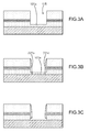
figures 3A-3C illustrent un autre exemple de procédé suivant l'invention, de réalisation de tranchées d'isolation à travers un substrat de type semi-conducteur sur isolant, - les
figures 4A-4C illustrent un exemple de procédé de réalisation de tranchées d'isolation profondes traversant partiellement la couche semi-conductrice de support d'un substrat de type semi-conducteur sur isolant, - Des parties identiques, similaires ou équivalentes des différentes figures portent les mêmes références numériques de façon à faciliter le passage d'une figure à l'autre.
- Les différentes parties représentées sur les figures ne le sont pas nécessairement selon une échelle uniforme, pour rendre les figures plus lisibles.
- Un exemple de procédé de réalisation de tranchées isolantes suivant l'invention, va à présent être décrit en liaison avec les
figures 2A-2G . - Le matériau de départ de ce procédé est un substrat de type semi-conducteur sur isolant, qui peut être de type SOI, et comprend une couche de support semi-conductrice 100 par exemple à base de Si, recouverte par une couche isolante 101 par exemple de SiO2, surmontée d'une fine couche semi-conductrice 102 par exemple à base de Si. Par « fine » couche semi-conductrice on entend une couche semi-conductrice d'épaisseur inférieure à 100 nanomètres, par exemple d'épaisseur comprise entre 2 et 100 nanomètres ou de l'ordre de 10 ou 20 nanomètres.
- La couche isolante 101 peut, quant à elle, avoir une épaisseur x comprise par exemple entre 25 et 150 nanomètres.
- On forme tout d'abord un masquage 112 recouvrant la fine couche semi-conductrice 102.
- Ce masquage 112 peut être isolant et formé par exemple d'un empilement de couches de matériaux diélectriques, avec, par exemple, une première fine couche diélectrique 110 à base de SiO2, recouverte par une deuxième couche diélectrique 111 à base d'un matériau diélectrique différent, par exemple du Si3N4, recouvrant la première fine couche diélectrique 110. Le masquage 112 peut être réalisé de manière à comporter au moins une ouverture 115 dévoilant la fine couche semi-conductrice 102 (
figure 2A ). - On effectue ensuite, à travers l'ouverture 115, une gravure de la fine couche semi-conductrice 102, puis d'une épaisseur donnée de la couche isolante 101, de manière à prolonger l'ouverture 115 qui débouche alors sur la couche isolante 101.
- Cette gravure peut être anisotrope. Un tel type de gravure permet de prolonger l'ouverture 115 sans l'élargir. La gravure anisotrope peut être par exemple une gravure sèche réalisée par exemple par gravure ionique réactive communément appelée RIE (RIE pour « Reactive Ion Etching »). La gravure est réalisée de manière à conserver une épaisseur donnée e1 de la couche isolante 101, qui peut être par exemple comprise entre 20% et 80% de son épaisseur initiale, ou comprise par exemple entre 5 nanomètres et 20 nanomètres (
figure 2B ). - Suite à cette gravure partielle de la couche isolante 101, une portion 101a d'épaisseur donnée e1 par exemple égale à la moitié x/2 de l'épaisseur x de la couche isolante 101, est conservée au fond de l'ouverture 115.
- Puis, on forme une couche 121 dite « de protection » d'épaisseur e2, comprise par exemple entre 3 nanomètres et 5 nanomètres, recouvrant notamment les parois verticales ainsi que le fond de l'ouverture 115, la portion de la couche isolante 111 située au fond de l'ouverture 115 étant recouverte par cette couche de protection 121 (
figure 2C ). - La couche 121 de protection peut être choisie par exemple à base d'un matériau différent de celui de la couche isolante 101, et en particulier à base d'un matériau qui peut être gravé de manière sélective vis-à-vis du matériau de la couche isolante 101. La couche 121 de protection peut être par exemple à base de Si3N4.
- On effectue ensuite un dopage de la couche de protection 121, en particulier d'une région 121a de cette dernière située au fond de l'ouverture 115. Des régions de la couche de protection situées de part et d'autre de l'ouverture 115 et reposant sur le masquage 112, sont également dopées.
- Ce dopage peut être réalisé par au moins une implantation ionique, par exemple à l'aide de H, et/ou de He, et/ou d'Ar.
- Un dopage de la portion 101a restante de la couche isolante 101 située au fond de l'ouverture 115 sous la couche de protection 121 est également effectué éventuellement lors de l'étape d'implantation de la région 121a ou lors d'une autre étape.
- Ce dopage peut être également effectué, à l'aide d'au moins une implantation ionique, par exemple à l'aide de H, et/ou de He, et/ou d'Ar.
- Pour doper la portion 101a de la couche isolante située au fond du trou 119, plusieurs implantations successives peuvent être effectuées.
- Une première implantation par exemple à l'aide d'Ar, selon une dose par exemple de 5*1015 et selon par exemple une énergie de l'ordre de 3 keV, suivie d'une deuxième implantation par exemple à l'aide d'Ar, selon une dose par exemple de 5*1015 et selon une énergie par exemple de l'ordre de 15 keV, peut être effectuée afin d'implanter une couche de protection 121 à base de nitrure d'épaisseur par exemple de l'ordre de 9 nm, ainsi qu'une portion 101a de la couche isolante d'épaisseur par exemple de l'ordre de 10 à 15 nanomètres.
- Ensuite, on effectue un retrait partiel de la couche de protection 121. Ce retrait peut être réalisé par gravure sélective de manière à supprimer des régions de la couche de protection 121 qui ont été dopées, tout en conservant des régions 121b, 121c de cette couche de protection 121 qui n'ont pas été dopées.
- Les régions 121b, 121c de la couche de protection 121 conservées tapissent une partie des parois verticales de l'ouverture 115, et en particulier recouvrent des zones de la fine couche semi-conductrice 102 et du masquage 112 dans l'ouverture 115.
- Un retrait de la portion 101a restante de la couche isolante 101 située au fond de l'ouverture 105, peut être réalisé par gravure sélective vis-à-vis du matériau de la couche de support 100, tandis que la fine couche semi-conductrice 102 et le masquage 112 sont protégés par les régions 121b, 121c de la couche de protection 121.
- Du fait du dopage de la portion restante 101a de la couche isolante 101 tandis que le reste de cette couche isolante 101 n'est pas dopé, une sélectivité de gravure entre cette portion 101a et le reste de la couche isolante 101 est également opéré.
- Cette sélectivité peut être par exemple de 4/1, de sorte que les parties non-dopées de la couche isolante 101 se consomment 4 fois plus lentement que la portion 101a dopée (
figure 2F ). - La gravure de la portion 101a restante de la couche isolante 101 peut être effectuée par exemple à l'aide de HF, par exemple au moyen d'une solution de gravure communément appelée BOE (BOE pour « buffered oxide etch ») composée d'un tampon, comme du fluorure d'ammonium (NH4F), et d'acide fluorhydrique (HF). Cette gravure peut conduire au retrait de zones de la couche isolante 101 situées à l'aplomb des régions 121a, 121b de la zone de protection.
- Ensuite, un retrait des régions 121a, 121b de protection est réalisé, par exemple à l'aide de H3PO4 (
figure 2G ). - Une variante de réalisation est illustrée sur les
figures 3A-3C . - Comme pour l'exemple de procédé précédemment décrit, on peut former un masquage 112 sur la fine couche semi-conductrice 102, puis réaliser au moins une ouverture 115 dans ce masquage 112.
- On grave ensuite partiellement la couche isolante 101 au fond de l'ouverture, en conservant une portion 101a de la couche isolante 101 (
figure 3A ). - On forme ensuite la couche de protection 121. Une gravure anisotrope de cette couche de protection 121 peut être ensuite gravée, par exemple à l'aide d'une gravure RIE (RIE pour « Reactive Ion Etching »). Cette gravure est réalisée de manière à conserver des régions 221b, 221c tapissant les parois verticales de l'ouverture 115, la portion 101a étant dévoilée au fond de l'ouverture 115 (
figure 3B ). - Cette gravure peut présenter une sélectivité entre le matériau de la couche de protection 121 et celui de la couche isolante 101.
- Puis, on réalise un dopage de la portion 101a dévoilée au fond de l'ouverture 115.
- Ensuite, on effectue un retrait de la portion restante 101a de la couche isolante 101 par gravure sélective vis-à-vis du reste de la couche isolante 101 (
figure 3C ). Cette gravure isolante 101 peut être par exemple une gravure sélective. - L'un ou l'autre des exemples de procédé décrits en liaison avec les
figures 2 et3 peuvent être utilisés au cours d'un procédé visant à réaliser des tranchées isolantes de profondeurs différentes. - Un autre exemple de procédé suivant l'invention va à présent être donné en liaison avec les
figures 4A-4C . - Comme dans l'un ou l'autre des exemples de procédés précédemment décrits, on forme tout d'abord un premier masquage 112 recouvrant la fine couche semi-conductrice 102 d'un substrat semi-conducteur sur isolant, le masquage 112 comportant des ouvertures 115a, 115b, 115c, 115d dévoilant la fine couche semi-conductrice 102.
- Puis, à travers les ouvertures 115a, 115b, 115c, 115d, une gravure de la fine couche semi-conductrice 102, puis d'une épaisseur donnée de la couche isolante 101, est effectuée par gravure anisotrope à travers les ouvertures 115a, 115b, 115c, 115d, de manière à conserver une épaisseur donnée de la couche isolante 101.
- Puis, comme dans les exemples de procédé décrits précédemment, on effectue un dopage de l'épaisseur donnée de la couche isolante 101a, que l'on grave ensuite de manière sélective vis-à-vis du reste de la couche isolante 101. Cette gravure est stoppée lorsque cette épaisseur est retirée et que l'on a atteint l'interface entre la couche isolante 101 et la couche de support 100.
- On obtient ainsi, une uniformité entre les profondeurs respectives des ouvertures 115a, 115b, 115c, 115d.
- Ensuite, on forme un deuxième masquage 212 par dessus le premier masquage 112. Ce deuxième masquage 212 peut être, par exemple, un masquage à base de résine photosensible et comporte des trous 215a, 215b, 215c, dévoilant chacun une ouverture parmi lesdites ouvertures 115a, 115c, 115d, formées dans le premier masquage 112. Le deuxième masquage 212 peut être réalisé de manière à combler au moins une ouverture 115b parmi les ouvertures du premier masquage (
figure 4B ). - Puis, on réalise des tranchées 230a, 230b, 230c à travers les trous 215a, 215b, 215c du deuxième masquage 212. Pour cela, on effectue une gravure de l'épaisseur restante de la couche isolante 101 située au fond des trous 215a, 215b, 215c, ainsi que de la couche semi-conductrice 100 de support dans le prolongement des ouvertures 115a, 115c, 115d. Cette gravure peut être réalisée par exemple à base de HBr/O2. Des tranchées profondes 231a, 231b, 231c, traversant une partie de l'épaisseur de la couche de support 100 sont ainsi réalisées (
figure 4C ). Ces tranchées profondes 231a, 231b, 231c, peuvent avoir une largeur ou dimension critique Wmin (la dimension critique ou largeur des tranchées étant leur plus petite dimension mesurée dans un plan parallèle au plan [O;i ;k ] du repère orthogonal [O;i ;j ;k ]) comprise par exemple, entre 30 et 100 nanomètres, ou par exemple de l'ordre de 50 nanomètres. Les tranchées profondes 231a, 231b, 231c peuvent également avoir une profondeur H comprise par exemple entre 50 nanomètres et 5 micromètres ou entre 50 nanomètres et 500 nanomètres, par exemple de 180 ou 200 nanomètres. - L'uniformité de profondeur entre les ouvertures 115a, 115b, 115d réalisées lors d'étape décrites précédemment en liaison avec la
figure 4A permet d'obtenir également une uniformité de profondeur entre les tranchées 231a, 231b, 231c traversant la couche de support 100. - On peut ensuite effectuer un remplissage des tranchées à l'aide d'un matériau diélectrique.
Claims (5)
- Procédé de réalisation d'une ou plusieurs tranchées dans un dispositif comprenant un substrat de type semi-conducteur sur isolant formé d'une couche semi-conductrice de support (100), d'une couche isolante (101) reposant sur la couche de support, et d'une couche semi-conductrice (102) reposant sur ladite couche isolante (101), le procédé comprenant des étapes de :a) dopage localisé d'une portion donnée (101a) de ladite couche isolante (101) à travers une ouverture (115, 115b) d'une couche de masquage (112) reposant sur la fine couche semi-conductrice (102),b) retrait par gravure sélective de ladite zone donnée dopée au fond de ladite ouverture.
- Procédé selon la revendication 1, comprenant préalablement à l'étape a), une étape de gravure anisotrope d'une épaisseur de la couche isolante à travers au moins une ouverture (115, 115b) d'une couche de masquage (112) reposant sur la fine couche semi-conductrice, ladite portion donnée correspondant à une épaisseur restante de ladite couche isolante (101) conservée au fond de ladite ouverture correspondante.
- Procédé selon la revendication 1 ou 2, dans lequel, lors de l'étape b), les parois de l'ouverture sont protégées par des zones de protection (121b, 121c).
- Procédé selon la revendication 3, les zones de protection ayant été formées par :- dépôt d'une couche de protection dans ladite ouverture (115) ,- dopage sélectif de la couche de protection au moins une région située au fond de ladite ouverture étant dopée,- retrait des régions dopées de ladite couche de protection.
- Procédé selon l'une des revendications 1 à 4, comprenant en outre après l'étape b), la gravure de la couche de support semi-conductrice dans le prolongement de ladite ouverture.
Applications Claiming Priority (1)
| Application Number | Priority Date | Filing Date | Title |
|---|---|---|---|
| FR1156854A FR2978611B1 (fr) | 2011-07-27 | 2011-07-27 | Procede ameliore de realisation de tranchees d'isolation dans un substrat semi-conducteur sur isolant |
Publications (1)
| Publication Number | Publication Date |
|---|---|
| EP2551899A1 true EP2551899A1 (fr) | 2013-01-30 |
Family
ID=46513676
Family Applications (1)
| Application Number | Title | Priority Date | Filing Date |
|---|---|---|---|
| EP12177539A Withdrawn EP2551899A1 (fr) | 2011-07-27 | 2012-07-23 | Procédé ameliore de réalisation de tranchées d'isolation dans un substrat semi-conducteur sur isolant |
Country Status (3)
| Country | Link |
|---|---|
| US (1) | US8735259B2 (fr) |
| EP (1) | EP2551899A1 (fr) |
| FR (1) | FR2978611B1 (fr) |
Cited By (1)
| Publication number | Priority date | Publication date | Assignee | Title |
|---|---|---|---|---|
| FR3061706A1 (fr) * | 2017-01-11 | 2018-07-13 | Commissariat Energie Atomique | Procede d'acces a un organe d'un dispositif microelectronique |
Families Citing this family (2)
| Publication number | Priority date | Publication date | Assignee | Title |
|---|---|---|---|---|
| CN106707649B (zh) * | 2017-03-01 | 2019-09-03 | 合肥京东方光电科技有限公司 | 过孔的制备方法、阵列基板的制备方法及阵列基板 |
| US11189546B2 (en) | 2019-10-18 | 2021-11-30 | Taiwan Semiconductor Manufacturing Company Limited | Semiconductor arrangement and method for making |
Citations (5)
| Publication number | Priority date | Publication date | Assignee | Title |
|---|---|---|---|---|
| KR20020006976A (ko) * | 2000-07-14 | 2002-01-26 | 윤종용 | 반도체 장치의 트렌치 형성 방법 |
| US20030153136A1 (en) * | 2002-02-14 | 2003-08-14 | Mitsubishi Denki Kabushiki Kaisha | Method of manufacturing semicontor device having trench isolation |
| US20030216044A1 (en) * | 2002-05-16 | 2003-11-20 | Nanya Technology Corporation | Method for forming bottle trenches |
| US20080213971A1 (en) | 2004-08-12 | 2008-09-04 | Renesas Technology Corp | Semiconductor device having dual-STI and manufacturing method thereof |
| US20080318391A1 (en) * | 2007-06-22 | 2008-12-25 | Ryu Sang-Wook | Method of manufacturing semiconductor device |
Family Cites Families (1)
| Publication number | Priority date | Publication date | Assignee | Title |
|---|---|---|---|---|
| US5313094A (en) * | 1992-01-28 | 1994-05-17 | International Business Machines Corportion | Thermal dissipation of integrated circuits using diamond paths |
-
2011
- 2011-07-27 FR FR1156854A patent/FR2978611B1/fr active Active
-
2012
- 2012-07-23 US US13/555,356 patent/US8735259B2/en active Active
- 2012-07-23 EP EP12177539A patent/EP2551899A1/fr not_active Withdrawn
Patent Citations (6)
| Publication number | Priority date | Publication date | Assignee | Title |
|---|---|---|---|---|
| KR20020006976A (ko) * | 2000-07-14 | 2002-01-26 | 윤종용 | 반도체 장치의 트렌치 형성 방법 |
| US20030153136A1 (en) * | 2002-02-14 | 2003-08-14 | Mitsubishi Denki Kabushiki Kaisha | Method of manufacturing semicontor device having trench isolation |
| US20030216044A1 (en) * | 2002-05-16 | 2003-11-20 | Nanya Technology Corporation | Method for forming bottle trenches |
| US20080213971A1 (en) | 2004-08-12 | 2008-09-04 | Renesas Technology Corp | Semiconductor device having dual-STI and manufacturing method thereof |
| US20110057287A1 (en) | 2004-08-12 | 2011-03-10 | Renesas Electronics Corporation | Semiconductor device having dual-sti and manufacturing method thereof |
| US20080318391A1 (en) * | 2007-06-22 | 2008-12-25 | Ryu Sang-Wook | Method of manufacturing semiconductor device |
Cited By (1)
| Publication number | Priority date | Publication date | Assignee | Title |
|---|---|---|---|---|
| FR3061706A1 (fr) * | 2017-01-11 | 2018-07-13 | Commissariat Energie Atomique | Procede d'acces a un organe d'un dispositif microelectronique |
Also Published As
| Publication number | Publication date |
|---|---|
| US8735259B2 (en) | 2014-05-27 |
| FR2978611B1 (fr) | 2013-08-16 |
| US20130189825A1 (en) | 2013-07-25 |
| FR2978611A1 (fr) | 2013-02-01 |
Similar Documents
| Publication | Publication Date | Title |
|---|---|---|
| EP1923912B1 (fr) | Procédé de fabrication d'une structure microtechnologique mixte | |
| EP3847693B1 (fr) | Procede de fabrication d'un dispositif cfet | |
| EP2840589B1 (fr) | Procédé améliore de séparation entre une zone activé d'un substrat et sa face arrière ou une portion de sa face arrière | |
| FR3060841A1 (fr) | Procede de realisation d'un dispositif semi-conducteur a espaceurs internes auto-alignes | |
| EP3850659A1 (fr) | Procédé de réalisation d'un substrat avancé pour une intégration hybride | |
| EP3531444A1 (fr) | Circuit intégré comprenant un substrat équipé d'une région riche en pièges, et procédé de fabrication | |
| EP3511293A1 (fr) | Procede de fabrication d'au moins un transistor a effet de champ | |
| EP2706565A1 (fr) | Dispositif microélectronique à tranchées d'isolation débordant sous une zone activé | |
| EP1428247B1 (fr) | Procede de fabrication d'un transistor a effet de champ a grilles auto-alignees horizontales | |
| EP1589572B1 (fr) | Procédé de fabrication d'un circuit intégré comprenant l'élaboration de tranchées d'isolation creuses | |
| FR2978611A1 (fr) | Procede ameliore de realisation de tranchees d'isolation dans un substrat semi-conducteur sur isolant | |
| FR2991502A1 (fr) | Procede de fabrication d'un circuit integre ayant des tranchees d'isolation avec des profondeurs distinctes | |
| FR3085085A1 (fr) | Transistor a barreaux superposes et structure double-grille | |
| EP4091197A1 (fr) | Procédé de fabrication d'un capteur d'image | |
| FR2718287A1 (fr) | Procédé de fabrication d'un transistor à effet de champ à grille isolée, en particulier de longueur de canal réduite, et transistor correspondant. | |
| FR3050315B1 (fr) | Transistor a overlap des regions d'acces maitrise | |
| FR3035265A1 (fr) | Procede de fabrication de transistors soi pour une densite d'integration accrue | |
| FR3019937A1 (fr) | Procede de formation de tranchees d'isolement | |
| EP3007218B1 (fr) | Structure d'encapsulation d'un nano-objet pourvue d'un capot et d'un substrat avec reprise de contact au travers du capot, et son procede de fabrication | |
| EP4123692A1 (fr) | Procede de fabrication d'un substrat semi-conducteur sur isolant de type soi ou sigeoi par besoi et structure pour fabriquer un tel substrat | |
| FR2865850A1 (fr) | Procede de realisation d'un transistor a effet de champ et transistor ainsi obtenu | |
| EP3944322B1 (fr) | Procédé de fabrication d'un dispositif microélectronique | |
| FR3109017A1 (fr) | PROCÉDÉ DE FABRICATION D’UNE PUCE À CIRCUIT INTÉGRÉ sur SeOI | |
| FR3091016A1 (fr) | Circuit 3d dote d’une isolation mesa pour la zone de plan de masse | |
| FR3084519A1 (fr) | Realisation de circuit 3d avec transistor de niveau superieur dote d'un dielectrique de grille issu d'un report de substrat |
Legal Events
| Date | Code | Title | Description |
|---|---|---|---|
| PUAI | Public reference made under article 153(3) epc to a published international application that has entered the european phase |
Free format text: ORIGINAL CODE: 0009012 |
|
| AK | Designated contracting states |
Kind code of ref document: A1 Designated state(s): AL AT BE BG CH CY CZ DE DK EE ES FI FR GB GR HR HU IE IS IT LI LT LU LV MC MK MT NL NO PL PT RO RS SE SI SK SM TR |
|
| AX | Request for extension of the european patent |
Extension state: BA ME |
|
| 17P | Request for examination filed |
Effective date: 20130612 |
|
| RBV | Designated contracting states (corrected) |
Designated state(s): AL AT BE BG CH CY CZ DE DK EE ES FI FR GB GR HR HU IE IS IT LI LT LU LV MC MK MT NL NO PL PT RO RS SE SI SK SM TR |
|
| 17Q | First examination report despatched |
Effective date: 20131014 |
|
| STAA | Information on the status of an ep patent application or granted ep patent |
Free format text: STATUS: THE APPLICATION IS DEEMED TO BE WITHDRAWN |
|
| 18D | Application deemed to be withdrawn |
Effective date: 20160202 |